JP2010045169A - Compound semiconductor device and method of manufacturing the same - Google Patents
Compound semiconductor device and method of manufacturing the same Download PDFInfo
- Publication number
- JP2010045169A JP2010045169A JP2008207890A JP2008207890A JP2010045169A JP 2010045169 A JP2010045169 A JP 2010045169A JP 2008207890 A JP2008207890 A JP 2008207890A JP 2008207890 A JP2008207890 A JP 2008207890A JP 2010045169 A JP2010045169 A JP 2010045169A
- Authority
- JP
- Japan
- Prior art keywords
- compound semiconductor
- semiconductor layer
- layer
- based compound
- semiconductor device
- Prior art date
- Legal status (The legal status is an assumption and is not a legal conclusion. Google has not performed a legal analysis and makes no representation as to the accuracy of the status listed.)
- Granted
Links
Images


Abstract
Description
本発明は、化合物半導体装置とその製造方法に関し、特にV族元素としてAsを含む層とAsを含まない層とが積層された化合物半導体装置に関する。 The present invention relates to a compound semiconductor device and a manufacturing method thereof, and more particularly to a compound semiconductor device in which a layer containing As as a group V element and a layer not containing As are stacked.
GaAs基板、InP基板上にジンクブレンド結晶構造を有するIII−V族化合物半導体層を成長して種々の半導体装置が形成されている。異なるIII−V族半導体の層を積層したヘテロ構造を用いた半導体装置として、高電子移動度トランジスタ(HEMT)等の電界効果トランジスタ、ヘテロ接合バイポーラトランジスタ、発光装置、多層膜光学フィルタ等が知られている。 Various semiconductor devices are formed by growing a III-V compound semiconductor layer having a zinc blend crystal structure on a GaAs substrate and an InP substrate. As semiconductor devices using a heterostructure in which different III-V group semiconductor layers are stacked, field effect transistors such as high electron mobility transistors (HEMT), heterojunction bipolar transistors, light emitting devices, multilayer optical filters, and the like are known. ing.
例えば、半絶縁性(semi-insulating, si-)GaAs基板上に、必要に応じて真性(i型)GaAsバッファ層を介してi型GaAsまたはi型InGaAsのチャネル(電子走行)層、n型AlGaAsの電子供給層、n型GaAsまたはInGaAsのコンタクト層を順次エピタキシャル成長し、ゲートコンタクト領域のコンタクト層をエッチングして除去し、電子供給層上にショットキコンタクトするゲート電極、その両側のコンタクト層上にオーミックコンタクトするソース/ドレイン電極を形成してHEMTを作成することが知られている。チャネル層の上下に電子供給層を設けてもよい。電子供給層をn型層とその少なくとも一方の側に設けたスペーサ層で構成してもよい。 For example, on a semi-insulating (si-) GaAs substrate, an i-type GaAs or i-type InGaAs channel (electron transit) layer, an n-type via an intrinsic (i-type) GaAs buffer layer as required. The AlGaAs electron supply layer and the n-type GaAs or InGaAs contact layer are epitaxially grown in sequence, the contact layer in the gate contact region is removed by etching, and a Schottky contact is formed on the electron supply layer, on the contact layers on both sides thereof. It is known to form a HEMT by forming source / drain electrodes that are in ohmic contact. Electron supply layers may be provided above and below the channel layer. The electron supply layer may be composed of an n-type layer and a spacer layer provided on at least one side thereof.
GaAs,AlGaAs,InGaAs等、V族元素がAsであるIII−V族化合物半導体を、III族元素に拘わらず、As系化合物半導体と呼ぶことにする。同様、V族元素がPであるIII−V族化合物半導体をP系化合物半導体と呼ぶことにする。 A group III-V compound semiconductor in which the group V element is As, such as GaAs, AlGaAs, or InGaAs, will be referred to as an As-based compound semiconductor regardless of the group III element. Similarly, a group III-V compound semiconductor in which the group V element is P is referred to as a P-based compound semiconductor.
上述のHEMT構造において、As系化合物半導体であるコンタクト層とその下方のAs系化合物半導体である電子供給層との間に、P系化合物半導体であるGaInP層を挿入し、エッチングストッパとして用いることも知られている。例えば、リン酸、過酸化水素水、純水を1:1:12で混合した燐酸系エッチング溶液はAs系化合物半導体は高速でエッチングし、P系化合物半導体はほとんどエッチングしない。このようなエッチングストッパ層を用いてコンタクト層をエッチングすれば、エッチングストッパ層より下側の層をエッチングから保護することができる。 In the HEMT structure described above, a GaInP layer, which is a P-based compound semiconductor, is inserted between a contact layer, which is an As-based compound semiconductor, and an electron supply layer, which is an As-based compound semiconductor, below the contact layer, and can be used as an etching stopper. Are known. For example, a phosphoric acid etching solution in which phosphoric acid, hydrogen peroxide water, and pure water are mixed at 1: 1: 12 etches an As compound semiconductor at a high speed and hardly etches a P compound semiconductor. If the contact layer is etched using such an etching stopper layer, the layer below the etching stopper layer can be protected from etching.
特開2001−93838号は、トリメチルガリウム(TMG)、トリメチルインジウム(TMI)等の有機金属をIII族原料、アルシン(AsH3),ホスフィン(PH3)をV族原料とした気相成長において、AS原料の供給を停止してP原料の供給を行なっても、リアクタやチャンバ内に残留したAsが成長中のP系化合物薄膜中に混入して10〜30%のAsを含有したエッチングストッパ層を形成してしまい、燐酸系エッチング液でエッチされてしまうと指摘し、エッチングストッパ層を成長させる工程中、P原料のみの供給を行なう工程を一回以上設けることを提案する。 Japanese Patent Laid-Open No. 2001-93838 discloses vapor phase growth in which an organic metal such as trimethylgallium (TMG) and trimethylindium (TMI) is used as a group III material, and arsine (AsH 3 ) and phosphine (PH 3 ) as a group V material. Even if the supply of the AS raw material is stopped and the supply of the P raw material is performed, the etching stopper layer containing 10 to 30% As is mixed in the growing P-based compound thin film in the reactor or chamber. In the process of growing the etching stopper layer, it is proposed to provide at least one step of supplying only the P raw material during the step of growing the etching stopper layer.
特開2008−153440号は、GaAs基板上に、アンドープAlGaAsバッファ槽、アンドープAlGaAs障壁層、n型AlGaAs電子供給層、アンドープAlGaAsスペーサ層、アンドープInGaAsチャネル層、アンドープAlGaAsスペーサ層、n型AlGaAs電子供給層、n型AlGaAsスペーサ層、n型InGaP第1挿入層、n型AlGaAsゲート形成層、n型InGaP第2挿入層をエピタキシャル成長し、レジストマスクを用いてn型InGaP第2挿入層を塩酸系エッチング液でエッチしてn型AlGaAsゲート形成層でストップさせ、燐酸系エッチング液でn型AlGaAsゲート形成層をエッチしてn型InGaP第1挿入層でストップさせる電界効果トランジスタの製造方法を開示する。 JP 2008-153440 discloses an undoped AlGaAs buffer tank, an undoped AlGaAs barrier layer, an n-type AlGaAs electron supply layer, an undoped AlGaAs spacer layer, an undoped InGaAs channel layer, an undoped AlGaAs spacer layer, an n-type AlGaAs electron supply on a GaAs substrate. An n-type AlGaAs spacer layer, an n-type InGaP first insertion layer, an n-type AlGaAs gate forming layer and an n-type InGaP second insertion layer are epitaxially grown, and the n-type InGaP second insertion layer is etched with hydrochloric acid using a resist mask A method of manufacturing a field effect transistor is disclosed in which an n-type AlGaAs gate formation layer is etched with a liquid and stopped at a n-type AlGaAs gate formation layer, and an n-type AlGaAs gate formation layer is etched with a phosphoric acid-based etchant and stopped at a first n-type InGaP insertion layer.
V族元素がPであるP系化合物半導体層とV族元素がAsであるAs系化合物半導体層を積層し、一方の層をエッチングストッパとして他方の層をエッチングすることがある。 A P-based compound semiconductor layer in which the V group element is P and an As-based compound semiconductor layer in which the V group element is As may be stacked, and the other layer may be etched using one layer as an etching stopper.
P系化合物半導体層を形成することが望まれる時、P−As混合化合物半導体層が形成されてしまうと所望の機能が発揮できず、歩留まりが低下する原因になる。 When it is desired to form a P-based compound semiconductor layer, if the P-As mixed compound semiconductor layer is formed, a desired function cannot be exhibited, which causes a decrease in yield.
本発明の目的は、隣接するAs系半導体層からのAsの拡散を防止できるP系化合物半導体層を成長できる化合物半導体装置の製造方法、および結果として得られるP系化合物半導体層を含む化合物半導体装置を提供することである。 An object of the present invention is to provide a method of manufacturing a compound semiconductor device capable of growing a P-based compound semiconductor layer capable of preventing diffusion of As from an adjacent As-based semiconductor layer, and a compound semiconductor device including the resulting P-based compound semiconductor layer Is to provide.
本発明の他の目的は、十分薄く、かつエッチングスットッパとして十分機能するP系化合物半導体層を含む化合物半導体装置、およびその製造方法を提供することである。 Another object of the present invention is to provide a compound semiconductor device including a P-based compound semiconductor layer that is sufficiently thin and sufficiently functions as an etching stopper, and a manufacturing method thereof.
本発明の1観点によれば、
As濃度5×10¹⁷atoms/cm3〜3×1019atoms/cm3の範囲のAsを成長時にドーピングされている、V族元素がPである第1のP系化合物半導体層と、
前記第1のP系化合物半導体層の上に形成され、V族元素がAsである第1のAs系化合物半導体層と、
を有する化合物半導体装置
が提供される。
According to one aspect of the present invention,
A first P-based compound semiconductor layer in which an As concentration in the range of 5 × 10 17 atoms / cm 3 to 3 × 10 19 atoms / cm 3 is doped during growth, and a group V element is P;
A first As-based compound semiconductor layer formed on the first P-based compound semiconductor layer, wherein the group V element is As;
A compound semiconductor device is provided.
本発明の他の観点によれば、
(x)As濃度5×10¹⁷atoms/cm3〜3×1019atoms/cm3の範囲のAsをドーピングしつつ、V族元素がPである第1のP系化合物半導体層を形成する工程と、
(y)前記第1のP系化合物半導体層の上にV族元素がAsである第1のAs系化合物半導体層を形成する工程と、
を含む化合物半導体装置の製造方法
が提供される。
According to another aspect of the invention,
(X) A step of forming a first P-based compound semiconductor layer in which the group V element is P while doping As in the range of As
(Y) forming a first As compound semiconductor layer in which a group V element is As on the first P compound compound semiconductor layer;
The manufacturing method of the compound semiconductor device containing this is provided.
本発明者らは、不純物濃度レベルのAsをドープしたP系化合物半導体層を成長すると、隣接するAs系化合物半導体層からのAsの拡散を抑制できることを見出した。 The present inventors have found that when a P-based compound semiconductor layer doped with As at an impurity concentration level is grown, diffusion of As from an adjacent As-based compound semiconductor layer can be suppressed.
以下、本発明者らが行なった実験に沿って説明する。 In the following, description will be made along with experiments conducted by the present inventors.
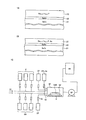
図1A,1Bは、予備実験において作成したサンプルの構成を概略的に示すGaAs基板の断面図である。図1Aにおいては、GaAs基板21の上に、アンドープGaAsバッファ層22、アンドープGa0.5In0.5P層23を順次有機金属化学気相堆積(MOCVD)で成長させた。図1Bにおいては、GaAs基板21の上に、アンドープGaAsバッファ層22、AsドープGa0.5In0.5P層25を順次MOCVDで成長させた。
1A and 1B are cross-sectional views of a GaAs substrate schematically showing the configuration of a sample prepared in a preliminary experiment. In FIG. 1A, an undoped GaAs
図1Cは、MOCVD装置の構成を示すブロック図である。反応炉RFは、ヒータHを備えた支持台SPを収容し、支持台SP上に成長用基板SUBを載置する。反応炉RFには複数のガス供給系GSが接続され、各ガス供給系GSには、マスフローコントローラと圧力計を含むガス制御装置GC。キャリアガス配管が接続されている。反応炉RFは真空排気ポンプVPによって所望圧力に維持され、徐害設備PRを介して排気される。 FIG. 1C is a block diagram showing the configuration of the MOCVD apparatus. The reaction furnace RF accommodates a support base SP provided with a heater H, and places the growth substrate SUB on the support base SP. A plurality of gas supply systems GS are connected to the reaction furnace RF, and each gas supply system GS includes a gas control device GC including a mass flow controller and a pressure gauge. Carrier gas piping is connected. The reaction furnace RF is maintained at a desired pressure by the vacuum exhaust pump VP, and is exhausted through the slow harm equipment PR.
V族原料ガス供給系、III族原料ガス供給系は、それぞれのキャリアガス配管に、ガス制御装置を介してV族原料ガス源、III族原料ガス源が接続されている。V族原料ガスは、アルシン(AsH3)とホスフィン(PH3)である。III族原料ガスは有機金属であり、トリメチルアルミニウム(TMA),トリメチルガリウム(TMG),トリメチルインジウム(TMI)を用いた。 In the group V source gas supply system and the group III source gas supply system, a group V source gas source and a group III source gas source are connected to respective carrier gas pipes via a gas control device. The group V source gas is arsine (AsH 3 ) and phosphine (PH 3 ). The group III source gas is an organic metal, and trimethylaluminum (TMA), trimethylgallium (TMG), and trimethylindium (TMI) were used.
ドーピング原料DPは、n型不純物、p型不純物それぞれ独立に供給される。n型ドーピング源として、シラン(SiH4)、セレン化水素(H2Se)、p型ドーピング源としてジメチルジンク(DMZn)が設けられている。 The doping material DP is supplied independently for each of the n-type impurity and the p-type impurity. As n-type doping source, silane (SiH 4), hydrogen selenide (H 2 Se), dimethyl zinc (DMZn) is provided as a p-type doping source.
さらに砒素が別配管で供給される。砒素のドーピング源として、水素で0.5%に希釈した希釈アルシンDILAsを用いた。 Furthermore, arsenic is supplied by a separate pipe. Diluted arsine DILAs diluted to 0.5% with hydrogen was used as the arsenic doping source.
成長温度は760℃、成長圧力は10kPa、III族原料の反応炉への供給量は200μmol/minに保った。ドーピングする砒素濃度の制御に関して、反応炉に供給される砒素供給量(モル)とIII族原料の供給量(モル)の比からAs/III比を定義する。 The growth temperature was 760 ° C., the growth pressure was 10 kPa, and the supply amount of the group III raw material to the reactor was kept at 200 μmol / min. Regarding the control of the arsenic concentration to be doped, the As / III ratio is defined from the ratio of the arsenic supply amount (mol) supplied to the reactor and the supply amount (mol) of the group III raw material.
図1Aにおいて、GaAs基板21の上に順次アンドープGaAsバッファ層22、アンドープGa0.5In0.5P層23を図1Cに示すMOCVD装置を用いて成長した。アンドープGa0.5In0.5P層23の成長は、V族原料の供給量を変化させて、V/III(モル)比を10〜450で変化させた。ここでのV族原料はホスフィンPH3である。
In FIG. 1A, an undoped GaAs
図1Bにおいて、GaAs基板21の上に順次アンドープGaAsバッファ層22、AsドープGa0.5In0.5P層25を図1Cに示すMOCVD装置を用いて成長した。AsドープGa0.5In0.5P層23の成長は、V族原料の供給量を変化させて、V/III(モル)比を20〜450で変化させ、As/III比を1.0×10−4〜1.0×10−1の範囲で変化させて行なった。
In FIG. 1B, an undoped GaAs
作成したサンプルのエピタキシャルGa0.5In0.5P層中の砒素濃度を2次イオン質量分析(SIMS)により測定した。アンドープGa0.5In0.5P層23には、意図的なAsドープは行なっていない。しかし、アンドープGa0.5In0.5P層23中の砒素濃度分布は、アンドープGaAsバッファ層22との界面で高く、界面から離れるに従って減少し、AsがGaAs層から拡散したと考えられる。As濃度が母体であるGa0.5In0.5P層23のV族元素であるPの原子数に対して5%以下になる距離を拡散距離と規定して拡散距離を測定した。同様に、AsドープGa0.5In0.5P層25中のAs濃度分布を測定し、As拡散距離を測定した。
The epitaxial Ga 0.5 an In 0.5 arsenic concentration of the P layer of the samples prepared was measured by secondary ion mass spectroscopy (SIMS). The undoped Ga 0.5 In 0.5
図2は、測定した砒素の拡散距離をV/III比の関数として示すグラフである。横軸がV/III比を示し、縦軸がAs拡散距離を単位nmで示す。アンドープGa0.5In0.5P層23中Asの拡散距離を■で示し、AsドープGa0.5In0.5P層25中のAsの拡散距離を□で示す。アンドープGa0.5In0.5P層23中Asの拡散距離が、AsドープGa0.5In0.5P層25中のAsの拡散距離より大幅に大きいことがわかる。アンドープGa0.5In0.5P層23中Asの拡散距離は、V/III比の低い領域で高く、V/III比の増大と共に急激に減少するが、V/III比10では120nm以上、V/III比20で約78である。V/III比を好適な値に選択してもAs拡散距離は45nm程度以上である。エッチングストッパとして機能するAs濃度5%以下のGa0.5In0.5P層23を形成するためには、厚さ50nm程度以上のGa0.5In0.5P層23を成長することが必要となろう。
FIG. 2 is a graph showing the measured arsenic diffusion distance as a function of the V / III ratio. The horizontal axis indicates the V / III ratio, and the vertical axis indicates the As diffusion distance in the unit of nm. The diffusion distance of As in the undoped Ga 0.5 In 0.5
アンドープGa0.5In0.5Pエッチングストッパ層を厚さ50nm程度以上形成すると、ソース/ドレインの抵抗成分が増大してしまう。 When the undoped Ga 0.5 In 0.5 P etching stopper layer is formed with a thickness of about 50 nm or more, the resistance component of the source / drain increases.
AsドープGa0.5In0.5P層25中のAsの拡散距離は16nm以下であり、V/III比に対する依存性も低い。広いV/III比の領域で10nm以下のAs拡散距離を実現可能である。厚さ十数nm以下のエッチングストッパ層を実現可能で、ソース/ドレインの抵抗成分増大を抑制することができる。次に、AsドープGa0.5In0.5P層25中のAsの拡散長のAs濃度に対する依存性を調べた。
The diffusion distance of As in the As-doped Ga 0.5 In 0.5
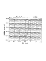
図3は、Asの拡散長のAs濃度に対する変化を、V/III比をパラメータとして調べた結果を示すグラフである。横軸がAs濃度を単位cm−3で示し、縦軸がAsの拡散長を単位nmで示す。V/III比を20,40,60,80,130,350,450とした場合を一緒に示す。As濃度1×1018cm−3以下のAs濃度領域では、V/III比の増大と共にAsの拡散長が減少する傾向がみられる。As濃度1×1018cm−3以上の領域ではV/III比依存性はほとんど見られない。V/III比に拘わらず、As濃度3×1017atoms/cm3〜5×1019atoms/cm3の範囲においてAs拡散長は30nm以下であり、Asアンドープの場合のAs拡散長45nm程度以上と比べ、明らかに短いAs拡散長を実現でき、界面でのAs組成変化を吸収にできる。さらに、As濃度5×1017atoms/cm3〜3×1019atoms/cm3の範囲においてAs拡散距離は十数nm以下である。V/III比を適切に選択すれば、As濃度5×1017atoms/cm3〜3×1019atoms/cm3の範囲において、As拡散長は10nm未満にできる。
FIG. 3 is a graph showing the results of examining the change of As diffusion length with respect to As concentration using the V / III ratio as a parameter. The horizontal axis indicates the As concentration in the unit cm −3 , and the vertical axis indicates the diffusion length of As in the unit nm. The cases where the V / III ratio is 20, 40, 60, 80, 130, 350, 450 are also shown. In an As concentration region with an As concentration of 1 × 10 18 cm −3 or less, the As diffusion length tends to decrease with an increase in the V / III ratio. In the region where the As concentration is 1 × 10 18 cm −3 or more, V / III ratio dependence is hardly observed. Regardless of the V / III ratio, the As diffusion length is 30 nm or less in the As concentration range of 3 × 10 17 atoms /
P系化合物半導体の成長時に、Asを5×10¹⁷atoms/cm3〜3×1019atoms/cm3の範囲でその場ドープすると、下地層などから成長層中へのAsが高濃度に取り込まれることを抑制できると考えられる。結果として、界面近傍を除きAs濃度が5×1017atoms/cm3〜3×1019atoms/cm3の範囲であるP系化合物半導体層が得られる。界面近傍のAs濃度は、隣接層からのAs拡散等により、より高濃度となり得る。このような場合を含めて、「As濃度5×1017atoms/cm3〜3×1019atoms/cm3の範囲のAsを成長時にドーピングされている、V族元素がPである第1のP系化合物半導体層」と呼ぶ。 When As is doped in the range of 5 × 10 17 atoms / cm 3 to 3 × 10 19 atoms / cm 3 during the growth of the P-based compound semiconductor, As is incorporated into the growth layer from the underlying layer in a high concentration. It is thought that it can be suppressed. As a result, a P-based compound semiconductor layer having an As concentration in the range of 5 × 10 17 atoms / cm 3 to 3 × 10 19 atoms / cm 3 except for the vicinity of the interface is obtained. The As concentration in the vicinity of the interface can be higher due to As diffusion from the adjacent layer. Including such a case, “As concentration of 5 × 10 17 atoms / cm 3 to 3 × 10 19 atoms / cm 3 of As is doped at the time of growth. It is called “P-based compound semiconductor layer”.
なお、As濃度5×10¹⁷atoms/cm3以下の範囲では、As濃度の減少と共にAs拡散長が増大している。Asアンドープとの差が減少するためと考えられる。As濃度3×1019atoms/cm3以上、特に5×1019atoms/cm3以上の範囲では、As濃度の増大と共にAs拡散長が増大している。As濃度が組成レベルになり、新たな機能を生じて、Asの拡散を抑制する機能を失っていくと考えられる。 In the range where the As concentration is 5 × 10 17 atoms / cm 3 or less, the As diffusion length increases as the As concentration decreases. This is probably because the difference from As undoped decreases. In the As concentration range of 3 × 10 19 atoms / cm 3 or more, particularly in the range of 5 × 10 19 atoms / cm 3 or more, the As diffusion length increases as the As concentration increases. It is considered that the As concentration becomes the composition level, a new function is generated, and the function of suppressing the diffusion of As is lost.
以上の実験結果から、以下のことが判る。P系化合物半導体にAsを適切な濃度で添加すると、P系化合物半導体へのAsの拡散を抑制できる。As濃度を対V族元素比で5%以下にするAs拡散長を十数nm以下に抑制することが容易であり、10nm未満にすることも可能である。エッチングストップ層としてP系化合物半導体を用いる場合を考えると、厚さ数nm〜十数nmでエッチングストッパ層としての機能を十分に備えたP系化合物半導体層が可能となる。
From the above experimental results, the following can be understood. When As is added to the P-based compound semiconductor at an appropriate concentration, the diffusion of As into the P-based compound semiconductor can be suppressed. It is easy to suppress the As diffusion length that makes the As
別の観点から見ると、As濃度分布の切り替えを急峻にすることができ、ヘテロ界面の境界を明確化できる。多層膜光学フィルタを形成する場合等、所望の光学的特性を有する多層膜を実現し易くなる。 From another point of view, the As concentration distribution can be switched sharply, and the boundary of the heterointerface can be clarified. When a multilayer optical filter is formed, a multilayer film having desired optical characteristics can be easily realized.
図4A−4Cは、電界効果トランジスタ(HEMT)の製造工程を示す断面図である。 4A to 4C are cross-sectional views illustrating manufacturing steps of a field effect transistor (HEMT).
図4Aに示すように、半絶縁性(si-)GaAs基板1の上に、厚さ200nmのアンドープ(i−)GaAsバッファ層2、厚さ100nmのアンドープ(i−)Al0.2Ga0.8As障壁層3、シート濃度が3×1012cm−2のSiプレーナドープ層4、厚さ3nmのi−Al0.2Ga0.8Asスペーサ層5、厚さ20nmのi−Al0.85Ga0.15Asチャネル層6、厚さ3nmのi−Al0.2Ga0.8Asスペーサ層7、シート濃度が3×1012cm−2のSiプレーナドープ層8、厚さ20nmのi−Al0.2Ga0.8Asショットキコンタクト層9、厚さ10nmのi−Ga0.52In0.48Pエッチングストッパ層10、キャリア濃度3×1018cm−3、厚さ30nmのn型GaAsオーミックコンタクト層11を順次MOCVDで成長する。
As shown in FIG. 4A, an undoped (i-) GaAs buffer layer 2 having a thickness of 200 nm and an undoped (i-) Al 0.2 Ga 0 having a thickness of 100 nm are formed on a semi-insulating (si-) GaAs substrate 1. .8 As barrier layer 3, Si planar doped layer 4 with a sheet concentration of 3 × 10 12 cm −2 , i-Al 0.2 Ga 0.8 As
i−Al0.85Ga0.15Asチャネル層6の下側に、Al0.2Ga0.8As障壁層3、Siプレーナドープ層4、i−Al0.2Ga0.8Asスペーサ層5で構成される電子供給層が配置され、i−Al0.85Ga0.15Asチャネル層6の上側に、i−Al0.2Ga0.8Asスペーサ層7、Siプレーナドープ層8、i−Al0.2Ga0.8Asショットキコンタクト層9で構成される電子供給層が配置されていると考えることができる。
Below the i-Al 0.85 Ga 0.15 As channel layer 6, an Al 0.2 Ga 0.8 As barrier layer 3, a Si planar doped layer 4, an i-Al 0.2 Ga 0.8 As spacer. is arranged constituted electron supply layer in the layer 5, the upper side of i-Al 0.85 Ga 0.15 As channel layer 6, i-Al 0.2 Ga 0.8 As
n型GaAsオーミックコンタクト層11は、ソース/ドレイン電極のチャネル層6に対するオーミック接触形成を容易にするための層である。ゲート電極は、上側の電子供給層上にショットキ接触するように形成する。ゲート電極形成領域のn型GaAsオーミックコンタクト層11は除去する必要がある。n型GaAsオーミックコンタクト層11エッチング時に、上側電子供給層にエッチングダメージを与えないように、i−Ga0.52In0.48Pエッチングストッパ層10が挿入されている。
The n-type GaAs
i−Ga0.52In0.48Pエッチングストッパ層10は、成長時にAsを種々の濃度でその場ドープして幾つかのサンプルを作成した。またAsアンドープにサンプルも作成した。
サンプルS1:Asアンドープ、
サンプルS2:Asドーピング量1.0×10¹⁸atoms/cm3、
サンプルS3:Asドーピング量5.0×10¹⁸atoms/cm3、
サンプルS4:Asドーピング量3.0×10¹⁹atoms/cm3、
サンプルS5:Asドーピング量8.0×10¹⁹atoms/cm3、
図4Bに示すように、n型GaAsオーミックコンタクト層11上にゲートコンタクト領域に開口を有するフォトレジストマスクPRを形成し、n型GaAsオーミックコンタクト層11を燐酸系エッチング液(燐酸:過酸化水素水;純水=1:1:12)でエッチングした。このエッチング液はAs系化合物半導体に対して高いエッチングレートを示すが、P系化合物半導体装置はほとんどエッチングしない。従って、i−Ga0.52In0.48Pエッチングストッパ層10は、燐酸系エッチング液を用いたn型GaAsオーミックコンタクト層11のエッチングにおいて、エッチングストッパとして機能すべき層である。但し、i−Ga0.52In0.48PにAsが添加され、As濃度が高くなるとエッチングストッパとしての機能が低下する。上記サンプルのエッチングストッパ層は厚さ10nmで形成したので、隣接するAs系化合物半導体層からのAs拡散で、層全体のAs濃度が高くなる可能性がある。
The i-Ga 0.52 In 0.48 P
Sample S1: As undoped,
Sample S2: As doping amount 1.0 × 10 18 atoms / cm 3 ,
Sample S3: As doping amount 5.0 × 10 18 atoms / cm 3 ,
Sample S4: As doping amount 3.0 × 10 19 atoms / cm 3 ,
Sample S5: As doping amount 8.0 × 10 19 atoms / cm 3 ,
As shown in FIG. 4B, a photoresist mask PR having an opening in the gate contact region is formed on the n-type GaAs
次に、露出したi−Ga0.52In0.48Pエッチングストッパ層10を塩酸系エッチング液でエッチングする。塩酸系エッチング液は、P系化合物半導体に対しては高いエッチングレートを示すが、As系化合物半導体に対するエッチングレートは著しく低い。従って、塩酸系エッチング液を用いたi−Ga0.52In0.48Pエッチングストッパ層10のエッチングにおいて、i−Al0.2Ga0.8Asショットキコンタクト層9はエッチングストッパとして機能する。その後、フォトレジストマスクPRは除去する。
Next, the exposed i-Ga 0.52 In 0.48 P
n型GaAsオーミックコンタクト層11のエッチング後、露出したi−Ga0.52In0.48Pエッチングストッパ層10表面を原子間力顕微鏡(AFM)で観察した。さらに、i−Ga0.52In0.48Pエッチングストッパ層10のエッチング後、i−Al0.2Ga0.8Asシショットキコンタクト層9表面もAFMで観察した。
After etching the n-type GaAs
サンプルS1においては、Asアンドープのi−Ga0.52In0.48Pエッチングストッパ層10の表面に孔状のエッチングダメージが高密度に観察された。さらに下層のi−Al0.2Ga0.8Asショットキコンタクト層9までもエッチングされ、同じく孔状のダメージを受けていることが判った。
In the sample S1, hole-like etching damage was observed at a high density on the surface of the As undoped i-Ga 0.52 In 0.48 P
サンプルS2においては、Asドープのi−Ga0.52In0.48Pエッチングストッパ層10の表面に孔状のエッチングダメージは観察されず、下層のi−Al0.2Ga0.8Asショットキコンタクト層9が保護されていることが判った。
In the sample S2 is hole-shaped etching damage to the surface of the i-Ga 0.52 In 0.48 P
サンプルS3,S4においても、Asドープのi−Ga0.52In0.48Pエッチングストッパ層10の表面に孔状のエッチングダメージは観察されず、下層のi−Al0.2Ga0.8Asショットキコンタクト層9が保護されていることが判った。
Also in the sample S3, S4, hole-shaped etching damage to the surface of the i-Ga 0.52 In 0.48 P
サンプルS5においては、Asドープのi−Ga0.52In0.48Pエッチングストッパ層10が全てエッチングで除去されており、さらに下層のi−Al0.2Ga0.8Asショットキコンタクト層9も全面にエッチングダメージを受けていることが判った。
In the sample S5, the As-doped i-Ga 0.52 In 0.48 P
図3を参照すると、i−Ga0.52In0.48Pエッチングストッパ層10がエッチングダメージを受けていないサンプルS2,S3,S4のAsドーピング量1.0×10¹⁸atoms/cm3、5.0×1018atoms/cm3、3.0×1019atoms/cm3は、As拡散長を10nm程度以下に抑制できるAsドーピング量である。厚さ10nmのi−Ga0.52In0.48Pエッチングストッパ層10表面のAs濃度は5%未満となって、エッチングストッパ層の機能を十分果たしたと考えられる。サンプルS5のAsドーピング量8.0×1019atoms/cm3は、As拡散長が50nm以上になるAsドーピング量である。厚さ10nmのi−Ga0.52In0.48Pエッチングストッパ層10は、全体のAs濃度が高くなり、エッチングストッパとして機能しなかったと考えられる。
Referring to FIG. 3, the As doping amount of samples S2, S3, and S4 in which the i-Ga 0.52 In 0.48 P
図2において、Asアンドープのi−Ga0.52In0.48P層中のAs拡散長は40nm以上である。サンプルS1の厚さ10nmのi−Ga0.52In0.48P層10は、エッチングストッパとして十分機能しなかったと考えられる。 In FIG. 2, the As diffusion length in the As undoped i-Ga 0.52 In 0.48 P layer is 40 nm or more. It is considered that the i-Ga 0.52 In 0.48 P layer 10 having a thickness of 10 nm of the sample S1 did not function sufficiently as an etching stopper.
サンプルS2,S3,S4のように、Asドーピング濃度1.0×10¹⁸atoms/cm3〜3.0×1019atoms/cm3のi−Ga0.52In0.48Pエッチングストッパ層を用いれば、厚さ10nmでもエッチングストッパの機能を十分果たすことができることが判った。 Like samples S2, S3, and S4, an i-Ga 0.52 In 0.48 P etching stopper layer having an As doping concentration of 1.0 × 10 18 atoms / cm 3 to 3.0 × 10 19 atoms / cm 3 is formed. It has been found that if used, the etching stopper function can be sufficiently achieved even with a thickness of 10 nm.
図4Cに示すように、n型GaAsオーミックコンタクト層11、i−Ga0.52In0.48Pエッチングストッパ層10のエッチング後、フォトレジストマスクPRは除去し、露出したi−Al0.2Ga0.8Asショットキコンタクト層9の上にショットキゲート電極13を形成し、n型GaAsオーミックコンタクト層11の上にソース/ドレイン電極14,15を形成する。このようにして、HEMTタイプの電界効果トランジスタが作成される。
As shown in FIG. 4C, after the n-type GaAs
図5は、GaAs基板上に、Asドーピング濃度1.0×10¹⁸atoms/cm3のGa0.5In0.5P層を厚さ約1μmMOCVDで成長し、表面からのAs濃度をSIMSで測定した結果を示すグラフである。横軸が表面からの深さを単位μmで示し、縦軸が砒素濃度を単位atoms/cm3で示す。GaAs基板表面から、成長層に向かってAs濃度が急峻に低下し、ほぼ拡散現象は生じていないことが判る。As系材料層とP系材料層を積層した時、界面での組成変化が急峻になることが示唆される。 FIG. 5 shows that a Ga 0.5 In 0.5 P layer with an As doping concentration of 1.0 × 10 18 atoms / cm 3 is grown on a GaAs substrate by MOCVD with a thickness of about 1 μm, and the As concentration from the surface is measured by SIMS. It is a graph which shows the measurement result. The horizontal axis indicates the depth from the surface in units of μm, and the vertical axis indicates the arsenic concentration in units of atoms / cm 3 . It can be seen that the As concentration sharply decreases from the surface of the GaAs substrate toward the growth layer, and almost no diffusion phenomenon occurs. It is suggested that the composition change at the interface becomes steep when the As-based material layer and the P-based material layer are laminated.
図6は、As系化合物半導体層28、P系化合物半導体層29が積相された構成を示す。例えば、多層膜光学フィルタとして機能する。この場合は、単結晶膜でなく、多結晶膜や、アモルファス膜であってもよい。複数種類の半導体デバイスを形成するための母材であってもよい。この場合は、単結晶層であることが好ましいであろう。
FIG. 6 shows a configuration in which an As-based
以上、実施例に沿って本発明を説明したが、本発明はこれらに制限されるものではない。例えば、MOCVDにおいて、III族原料としてトリエチルガリウム(TEG)等の他の有機金属や、V族原料としてターシャリブチルホスフィン(TBP)等の有機原料を用いてもよい。成長温度、成長圧力、III族原料の反応場への供給量等を種々変更することも可能である。GaInPエッチストッパ層にn型不純物をドープしてもよい。その他、種々の変更、置換、組み合わせ、改良等が可能なことは当業者に自明であろう。 As mentioned above, although this invention was demonstrated along the Example, this invention is not restrict | limited to these. For example, in MOCVD, another organic metal such as triethylgallium (TEG) may be used as a group III source, and an organic source such as tertiarybutylphosphine (TBP) may be used as a group V source. It is also possible to variously change the growth temperature, the growth pressure, the supply amount of the group III material to the reaction field, and the like. The GaInP etch stopper layer may be doped with n-type impurities. It will be apparent to those skilled in the art that various modifications, substitutions, combinations, improvements, and the like can be made.
1 GaAs基板、
2 i−GaAsバッファ層、
3 i−Al0.2Ga0.8Asバッファ層、
4、8 Siプレーナドープ層、
5,7 i−Al0.2Ga0.8Asスペーサ層、
6 i−Al0.85Ga0.15Asチャネル層、
9 i−Al0.2Ga0.8Asショットキコンタクト層、
10 i−Ga0.52In0.48Pエッチングストッパ層、
11 n−GaAsオーミックコンタクト層、
PR フォトレジストマスク、
13 ショットキゲート電極、
14,15 ソース/ドレイン電極、
21 GaAs基板、
22 GaAsバッファ層、
23 アンドープGa0.5In0.5P層、
25 AsドープGa0.5In0.5P層、
28 As系化合物半導体層、
29 P系化合物半導体層。
1 GaAs substrate,
2 i-GaAs buffer layer,
3 i-Al 0.2 Ga 0.8 As buffer layer,
4, 8 Si planar doped layer,
5,7 i-Al 0.2 Ga 0.8 As spacer layer,
6 i-Al 0.85 Ga 0.15 As channel layer,
9 i-Al 0.2 Ga 0.8 As Schottky contact layer,
10 i-Ga 0.52 In 0.48 P etching stopper layer,
11 n-GaAs ohmic contact layer,
PR photoresist mask,
13 Schottky gate electrode,
14, 15 source / drain electrodes,
21 GaAs substrate,
22 GaAs buffer layer,
23 undoped Ga 0.5 In 0.5 P layer,
25 As-doped Ga 0.5 In 0.5 P layer,
28 As compound semiconductor layer,
29 P-based compound semiconductor layer.
Claims (13)
前記第1のP系化合物半導体層の上に形成され、V族元素がAsである第1のAs系化合物半導体層と、
を有する化合物半導体装置。 A first P-based compound semiconductor layer in which an As concentration in the range of 3 × 10 17 atoms / cm 3 to 5 × 10 19 atoms / cm 3 is doped during growth, and a group V element is P;
A first As-based compound semiconductor layer formed on the first P-based compound semiconductor layer, wherein the group V element is As;
A compound semiconductor device having:
前記化合物半導体装置が電界効果トランジスタを構成する請求項1〜3のいずれか1項記載の化合物半導体装置。 The second As-based compound semiconductor layer is a GaAs or InGaAs channel layer, and the third As-based compound semiconductor layer is an AlGaAs electron supply layer doped with an n-type impurity;
The compound semiconductor device according to claim 1, wherein the compound semiconductor device constitutes a field effect transistor.
露出した前記第3のAs系化合物半導体層上に形成されたゲート電極と、
前記第1のAs系化合物半導体層の上に形成されたソース/ドレイン電極と、
を有する請求項4記載の化合物半導体装置。 The first As-based compound semiconductor layer and the first P-based compound semiconductor layer are etched away above a predetermined region of the third As-based compound semiconductor layer, so that the third As-based compound semiconductor layer is Exposed
A gate electrode formed on the exposed third As-based compound semiconductor layer;
A source / drain electrode formed on the first As-based compound semiconductor layer;
The compound semiconductor device according to claim 4, comprising:
(y)前記第1のP系化合物半導体層の上にV族元素がAsである第1のAs系化合物半導体層を形成する工程と、
を含む化合物半導体装置の製造方法。 (X) A step of forming a first P-based compound semiconductor layer in which the group V element is P while doping As in the range of As concentration 3 × 10 17 atoms / cm 3 to 5 × 10 19 atoms / cm 3. When,
(Y) forming a first As compound semiconductor layer in which a group V element is As on the first P compound compound semiconductor layer;
A method of manufacturing a compound semiconductor device comprising:
8. The step (x) involves irradiating the first P-based compound semiconductor layer while doping As in an As concentration range of 5 × 10 17 atoms / cm 3 to 3 × 10 19 atoms / cm 3. The manufacturing method of the compound semiconductor device of description.
を含む請求項7または8記載の化合物半導体装置の製造方法。 (A) before the step (x), forming a second As-based compound semiconductor layer and a third As-based compound semiconductor layer above the compound semiconductor substrate;
The manufacturing method of the compound semiconductor device of Claim 7 or 8 containing this.
を含む請求項9または10記載の化合物半導体装置の製造方法。 (B) After the step (y), the first P-based compound semiconductor layer is etched using a mask having an opening on a predetermined region of the first As-based compound semiconductor layer and a phosphoric acid-based etchant. Etching the first As-based compound semiconductor layer,
A method for manufacturing a compound semiconductor device according to claim 9 or 10, comprising:
(d)露出した前記第3のAs系化合物半導体層の上にゲート電極を形成する工程と、
(e)前記第1のAs系化合物半導体層の上にソース/ドレイン電極を形成する工程と、
を含む請求項11記載の化合物半導体装置の製造方法。 (C) following the step (b), etching the first P-based compound semiconductor layer using the mask and a hydrochloric acid-based etchant;
(D) forming a gate electrode on the exposed third As-based compound semiconductor layer;
(E) forming a source / drain electrode on the first As-based compound semiconductor layer;
The method for producing a compound semiconductor device according to claim 11, comprising:
Priority Applications (1)
| Application Number | Priority Date | Filing Date | Title |
|---|---|---|---|
| JP2008207890A JP5021585B2 (en) | 2008-08-12 | 2008-08-12 | Compound semiconductor device and manufacturing method thereof |
Applications Claiming Priority (1)
| Application Number | Priority Date | Filing Date | Title |
|---|---|---|---|
| JP2008207890A JP5021585B2 (en) | 2008-08-12 | 2008-08-12 | Compound semiconductor device and manufacturing method thereof |
Publications (2)
| Publication Number | Publication Date |
|---|---|
| JP2010045169A true JP2010045169A (en) | 2010-02-25 |
| JP5021585B2 JP5021585B2 (en) | 2012-09-12 |
Family
ID=42016324
Family Applications (1)
| Application Number | Title | Priority Date | Filing Date |
|---|---|---|---|
| JP2008207890A Expired - Fee Related JP5021585B2 (en) | 2008-08-12 | 2008-08-12 | Compound semiconductor device and manufacturing method thereof |
Country Status (1)
| Country | Link |
|---|---|
| JP (1) | JP5021585B2 (en) |
Citations (4)
| Publication number | Priority date | Publication date | Assignee | Title |
|---|---|---|---|---|
| JPS6450415A (en) * | 1987-08-20 | 1989-02-27 | Sanyo Electric Co | Manufacture of semiconductor device |
| JPH05251472A (en) * | 1992-01-09 | 1993-09-28 | Mitsubishi Electric Corp | Semiconductor device |
| JP2000332363A (en) * | 1998-11-09 | 2000-11-30 | Ricoh Co Ltd | Semiconductor luminous element and its manufacture |
| JP2001302389A (en) * | 2000-04-25 | 2001-10-31 | Nikko Materials Co Ltd | Vapor phase growing method |
-
2008
- 2008-08-12 JP JP2008207890A patent/JP5021585B2/en not_active Expired - Fee Related
Patent Citations (4)
| Publication number | Priority date | Publication date | Assignee | Title |
|---|---|---|---|---|
| JPS6450415A (en) * | 1987-08-20 | 1989-02-27 | Sanyo Electric Co | Manufacture of semiconductor device |
| JPH05251472A (en) * | 1992-01-09 | 1993-09-28 | Mitsubishi Electric Corp | Semiconductor device |
| JP2000332363A (en) * | 1998-11-09 | 2000-11-30 | Ricoh Co Ltd | Semiconductor luminous element and its manufacture |
| JP2001302389A (en) * | 2000-04-25 | 2001-10-31 | Nikko Materials Co Ltd | Vapor phase growing method |
Also Published As
| Publication number | Publication date |
|---|---|
| JP5021585B2 (en) | 2012-09-12 |
Similar Documents
| Publication | Publication Date | Title |
|---|---|---|
| JP2008263023A (en) | Manufacturing method of group iii-v compound semiconductor, schottky barrier diode, light-emitting diode, laser diode and manufacturing method of these | |
| JP2010045396A (en) | Method of manufacturing gallium nitride based semiconductor device | |
| US20160079370A1 (en) | Semiconductor device, semiconductor wafer, and semiconductor device manufacturing method | |
| JP2011249776A (en) | Semiconductor substrate, manufacturing method of semiconductor substrate, electronic device, manufacturing method of electronic device | |
| JP7169613B2 (en) | Manufacturing method of nitride semiconductor light emitting device | |
| JP5427623B2 (en) | Semiconductor substrate manufacturing method and semiconductor substrate | |
| JP2006313890A (en) | Gallium nitride based semiconductor device and method of manufacturing the same | |
| JP3158651B2 (en) | Compound semiconductor and method of manufacturing the same | |
| JP5746927B2 (en) | Semiconductor substrate, semiconductor device, and method of manufacturing semiconductor substrate | |
| JP5021585B2 (en) | Compound semiconductor device and manufacturing method thereof | |
| JP6028970B2 (en) | Semiconductor device manufacturing method and etching method | |
| JP2007258258A (en) | Nitride semiconductor element, and its structure and forming method | |
| US9859457B2 (en) | Semiconductor and template for growing semiconductors | |
| JP2000068497A (en) | GaN-BASED COMPOUND SEMICONDUCTOR DEVICE | |
| JP2011054685A (en) | Semiconductor substrate | |
| JP2013062442A (en) | Nitride semiconductor electronic device and nitride semiconductor electronic device manufacturing method | |
| CA2193098C (en) | Preparation of semiconductor substrates | |
| JP2016219590A (en) | Semiconductor substrate manufacturing method and semiconductor device manufacturing method | |
| JP7120334B2 (en) | Semiconductor device and method for manufacturing semiconductor device | |
| WO2010116701A1 (en) | Method for producing semiconductor substrate and semiconductor substrate | |
| US6036769A (en) | Preparation of semiconductor substrates | |
| JP3670130B2 (en) | Method for manufacturing group III-V compound semiconductor device | |
| JP3416051B2 (en) | Method for manufacturing group III-V compound semiconductor device | |
| JP2007235062A (en) | Epitaxial wafer, electronic device, and vapor phase epitaxial growth method of iii-v compound semiconductor crystal | |
| JP2005191477A (en) | Epitaxial wafer for high electron mobility transistor |
Legal Events
| Date | Code | Title | Description |
|---|---|---|---|
| A621 | Written request for application examination |
Free format text: JAPANESE INTERMEDIATE CODE: A621 Effective date: 20110725 |
|
| A977 | Report on retrieval |
Free format text: JAPANESE INTERMEDIATE CODE: A971007 Effective date: 20120418 |
|
| A131 | Notification of reasons for refusal |
Free format text: JAPANESE INTERMEDIATE CODE: A131 Effective date: 20120424 |
|
| A521 | Written amendment |
Free format text: JAPANESE INTERMEDIATE CODE: A523 Effective date: 20120517 |
|
| TRDD | Decision of grant or rejection written | ||
| A01 | Written decision to grant a patent or to grant a registration (utility model) |
Free format text: JAPANESE INTERMEDIATE CODE: A01 Effective date: 20120605 |
|
| A01 | Written decision to grant a patent or to grant a registration (utility model) |
Free format text: JAPANESE INTERMEDIATE CODE: A01 |
|
| A61 | First payment of annual fees (during grant procedure) |
Free format text: JAPANESE INTERMEDIATE CODE: A61 Effective date: 20120614 |
|
| R150 | Certificate of patent or registration of utility model |
Ref document number: 5021585 Country of ref document: JP Free format text: JAPANESE INTERMEDIATE CODE: R150 Free format text: JAPANESE INTERMEDIATE CODE: R150 |
|
| FPAY | Renewal fee payment (event date is renewal date of database) |
Free format text: PAYMENT UNTIL: 20150622 Year of fee payment: 3 |
|
| R250 | Receipt of annual fees |
Free format text: JAPANESE INTERMEDIATE CODE: R250 |
|
| R250 | Receipt of annual fees |
Free format text: JAPANESE INTERMEDIATE CODE: R250 |
|
| R250 | Receipt of annual fees |
Free format text: JAPANESE INTERMEDIATE CODE: R250 |
|
| R250 | Receipt of annual fees |
Free format text: JAPANESE INTERMEDIATE CODE: R250 |
|
| R250 | Receipt of annual fees |
Free format text: JAPANESE INTERMEDIATE CODE: R250 |
|
| LAPS | Cancellation because of no payment of annual fees |