JP2010034776A - Non-reciprocal circuit element - Google Patents
Non-reciprocal circuit element Download PDFInfo
- Publication number
- JP2010034776A JP2010034776A JP2008193685A JP2008193685A JP2010034776A JP 2010034776 A JP2010034776 A JP 2010034776A JP 2008193685 A JP2008193685 A JP 2008193685A JP 2008193685 A JP2008193685 A JP 2008193685A JP 2010034776 A JP2010034776 A JP 2010034776A
- Authority
- JP
- Japan
- Prior art keywords
- electrode
- ferrite
- circuit board
- soldered
- terminal electrode
- Prior art date
- Legal status (The legal status is an assumption and is not a legal conclusion. Google has not performed a legal analysis and makes no representation as to the accuracy of the status listed.)
- Granted
Links
Images


Abstract
Description
本発明は、非可逆回路素子、特に、マイクロ波帯で使用されるアイソレータやサーキュレータなどの非可逆回路素子に関する。 The present invention relates to a nonreciprocal circuit device, and more particularly to a nonreciprocal circuit device such as an isolator or a circulator used in a microwave band.
従来より、アイソレータやサーキュレータなどの非可逆回路素子は、予め定められた特定方向にのみ信号を伝送し、逆方向には伝送しない特性を有している。この特性を利用して、例えば、アイソレータは、自動車電話、携帯電話などの移動体通信機器の送信回路部に使用されている。 Conventionally, nonreciprocal circuit elements such as isolators and circulators have a characteristic of transmitting a signal only in a predetermined specific direction and not transmitting in a reverse direction. Utilizing this characteristic, for example, an isolator is used in a transmission circuit unit of a mobile communication device such as a car phone or a mobile phone.
この種の非可逆回路素子として、特許文献1に記載の2ポート型アイソレータでは、図9に示すように、フェライト32の互いに平行に位置する二つの主面に図示しない第1中心電極及び第2中心電極を互いに電気的に絶縁状態で交差して配置し、該フェライト32の主面に永久磁石41を接着剤42を介して固定し、フェライト・磁石素子30を構成している。このフェライト・磁石素子30は、回路基板20上の端子電極25,26,27にリフローはんだにて接続されている。即ち、入力部分35aが入力端子電極25にはんだ付けされ、出力部分35cが出力端子電極26にはんだ付けされ、グランド部分36lがグランド端子電極27にはんだ付けされている。
As this type of non-reciprocal circuit device, in the two-port isolator described in
前記アイソレータにおいて、入力部分35a、出力部分35c及びグランド部分36lがそれぞれの端子電極25,26,27にはんだ付けされるのは図9中斜線を付した部分である。一方の端部に位置する端子電極25,26はy方向に延在し、延在部分にはチップ型電子部品45(コンデンサ又は抵抗)がはんだ接続される。
In the isolator, the
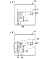
ところで、回路基板20上にフェライト・磁石素子30や電子部品45をリフローはんだで接合する際に、溶融したはんだの張力がy方向に大きく、反対のy’方向に小さいという不均衡な状態となり、フェライト・磁石素子30が図10(A)に示す正確な位置に接合されることなく、図10(B)に示すように、張力の大きいy方向にずれた状態で接合されてしまう。このようなずれが大きいと、電子部品45もフェライト・磁石素子30に押されて接合位置がずれてしまう。これでは、はんだ付けの信頼性が低下するのみならず、フェライト・磁石素子30と電子部品45や回路基板20に内蔵されている各種電子素子との位置関係が変化し、各素子間の残留インダクタンス値などが変動して特性のばらつきが大きくなる。
そこで、本発明の目的は、はんだ付け時におけるフェライト・磁石素子の位置ずれを効果的に防止し、はんだ付け信頼性の向上を図り、特性のばらつきを極力抑えることのできる非可逆回路素子を提供することにある。 Accordingly, an object of the present invention is to provide a non-reciprocal circuit element capable of effectively preventing misalignment of ferrite / magnet elements during soldering, improving soldering reliability, and minimizing variation in characteristics. There is to do.
前記目的を達成するため、本発明の一形態である非可逆回路素子は、
永久磁石と、
前記永久磁石により直流磁界が印加される直方体形状のフェライトと、
前記フェライトの互いに平行に位置する二つの主面に、互いに電気的に絶縁状態で交差して配置された導体膜からなる第1中心電極及び第2中心電極と、
表面に端子電極が形成された回路基板と、
を備え、
前記フェライトの主面に前記永久磁石を固定してフェライト・磁石素子が形成され、該フェライト・磁石素子は前記回路基板上にフェライトの主面が垂直方向に位置するように配置され、
前記回路基板の表面には、第1及び第2中心電極のそれぞれの端部がはんだ付けされる第1、第2及び第3端子電極が形成されており、第1及び第2端子電極は前記フェライトの長辺方向の一端部分に対向して配置され、第3端子電極は前記フェライトの長辺方向の他端部分に対向して配置されており、
第1及び第2端子電極の少なくともいずれかは前記フェライトの長辺方向とほぼ直交する第1の方向に延在され、第1及び第2端子電極の少なくともいずれかは前記第1の方向とはほぼ反対の第2の方向に延在されていること、
を特徴とする。
In order to achieve the above object, a non-reciprocal circuit device according to one aspect of the present invention comprises:
With permanent magnets,
A rectangular parallelepiped ferrite to which a DC magnetic field is applied by the permanent magnet,
A first center electrode and a second center electrode made of a conductor film disposed on two main surfaces of the ferrite that are located in parallel with each other and intersecting each other in an electrically insulated state;
A circuit board having terminal electrodes formed on the surface;
With
A ferrite magnet element is formed by fixing the permanent magnet to the main surface of the ferrite, and the ferrite magnet element is disposed on the circuit board so that the main surface of the ferrite is positioned in a vertical direction.
First, second, and third terminal electrodes are formed on the surface of the circuit board, to which the respective end portions of the first and second center electrodes are soldered. The third terminal electrode is arranged opposite to the other end portion of the ferrite in the long side direction, and is arranged to face one end portion in the long side direction of the ferrite,
At least one of the first and second terminal electrodes extends in a first direction substantially perpendicular to the long side direction of the ferrite, and at least one of the first and second terminal electrodes is the first direction. Extending in a substantially opposite second direction,
It is characterized by.
例えば、第1端子電極は第1中心電極の一端がはんだ付けされる入力端子電極であり、第2端子電極は第1中心電極の他端と第2中心電極の一端がはんだ付けされる出力端子電極であり、第3端子電極は第2中心電極の他端がはんだ付けされるグランド端子電極である。 For example, the first terminal electrode is an input terminal electrode to which one end of the first center electrode is soldered, and the second terminal electrode is an output terminal to which the other end of the first center electrode and one end of the second center electrode are soldered. The third terminal electrode is a ground terminal electrode to which the other end of the second center electrode is soldered.
前記非可逆回路素子において、フェライト・磁石素子がはんだ付けされる回路基板上の第1及び第2端子電極の少なくともいずれかは、第1の方向及びそれとは反対の第2の方向に延在されているため、リフローはんだ時に溶融したはんだの張力は第1及び第2の方向に均衡し、フェライト・磁石素子の接合位置がずれるおそれが解消される。 In the nonreciprocal circuit device, at least one of the first and second terminal electrodes on the circuit board to which the ferrite / magnet device is soldered extends in the first direction and the second direction opposite to the first direction. Therefore, the tension of the solder melted at the time of reflow soldering is balanced in the first and second directions, and the possibility that the joining position of the ferrite / magnet element is shifted is eliminated.
本発明によれば、フェライト・磁石素子が回路基板上にはんだ付けされる際の位置ずれを効果的に防止することができる。従って、はんだ付け信頼性が向上し、特性のばらつきが極力抑えられる。 According to the present invention, it is possible to effectively prevent displacement when the ferrite magnet element is soldered on the circuit board. Therefore, the soldering reliability is improved, and variations in characteristics are suppressed as much as possible.
以下、本発明に係る非可逆回路素子の実施例について添付図面を参照して説明する。 Embodiments of a nonreciprocal circuit device according to the present invention will be described below with reference to the accompanying drawings.
(第1実施例、図1〜図3参照)
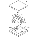
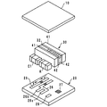
本発明に係る非可逆回路素子の第1実施例である2ポート型アイソレータの分解斜視図を図1に示す。この2ポート型アイソレータは、集中定数型アイソレータであり、概略、回路基板20と、フェライト32と一対の永久磁石41とからなるフェライト・磁石素子30と、平板状ヨーク10とで構成されている。
(Refer 1st Example and FIGS. 1-3)
FIG. 1 shows an exploded perspective view of a 2-port isolator which is a first embodiment of a nonreciprocal circuit device according to the present invention. This two-port isolator is a lumped constant type isolator, and generally includes a
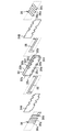
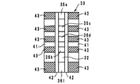
フェライト32には、図2に示すように、表裏の主面32a,32bに、絶縁材34A,34Bにて互いに電気的に絶縁された第1中心電極35及び第2中心電極36が形成されている。ここで、フェライト32は互いに平行な第1主面32a及び第2主面32bを有する直方体形状をなしている。
As shown in FIG. 2, the
また、永久磁石41はフェライト32に対して磁界を主面32a,32bに垂直方向に印加するように主面32a,32bに対向して、例えば、エポキシ系の接着剤42(図1参照)を介して接着され、フェライト・磁石素子30を形成している。永久磁石41の主面はフェライト32の主面32a,32bと同一寸法であり、互いの外形が一致するように主面どうしを対向させて配置されている。
Further, the
第1中心電極35は導体膜にて形成されている。即ち、図2に示すように、この第1中心電極35は、フェライト32の下面に形成された接続用電極35aに接続された状態で第1主面32aにおいて左下から立ち上がってほぼ水平方向に形成され、右上方に立ち上がって上面の中継用電極35bを介して第2主面32bに回り込む。第2主面32bにおいて、第1中心電極35は、第1主面32aと透視状態でほぼ重なるように形成され、その端部は下面に形成された接続用電極35cに接続されている。このように、第1中心電極35はフェライト32に1ターン巻回されている。そして、第1中心電極35と第2中心電極36とは、間に絶縁材34A,34Bが形成されて互いに絶縁された状態で交差している。中心電極35,36の交差角は必要に応じて設定され、入力インピーダンスや挿入損失が調整されることになる。
The
第2中心電極36は導体膜にて形成されている。この第2中心電極36は、まず、0.5ターン目36aがフェライト32の下面に形成された接続用電極35cと接続された状態で第2主面32bにおいて第1中心電極35と斜めに交差する状態で立ち上がり、上面の中継用電極36bを介して第1主面32aに回り込み、1ターン目36cが第1主面32aにおいて第1中心電極35と直交する状態で形成されている。1ターン目36cの下端部は下面の中継用電極36dを介して第2主面32bに回り込み、1.5ターン目36eが第2主面32bにおいて立ち上がり、上面の中継用電極36fを介して第1主面32aに回り込んでいる。以下同様に、2ターン目36g、中継用電極36h、2.5ターン目36i、中継用電極36j、3ターン目36kがフェライト32の表面にそれぞれ形成されている。3ターン目36kの下端部はフェライト32の下面に形成した接続用電極36lに接続されている。
The
前記接続用電極35a,35c,36lや中継用電極35b,36b,36d,36f,36h,36jは、フェライト32の上下面に形成された凹部に電極用導体を塗布又は充填して形成されている。この種の電極は、マザーフェライト基板に予めスルーホールを形成し、このスルーホールを電極用導体で充填した後、スルーホールを分断する位置でカットすることによって形成される。なお、各種電極はスルーホールに導体膜として形成したものであってもよい。また、多数個取りの手法で製作される場合、マザーフェライト基板に接着剤を介して永久磁石をも積層した状態でカットされることもある。
The
永久磁石41は、通常、ストロンチウム系、バリウム系、ランタン−コバルト系のフェライトマグネットが用いられる。永久磁石41とフェライト32とを接着する接着剤42としては、一液性の熱硬化型エポキシ接着剤を用いることが最適である。
As the
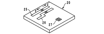
回路基板20は、複数枚の誘電体シート上に所定の電極を形成して積層し、焼結した積層型基板であり、その内部には、等価回路である図3に示すように、整合用コンデンサC1,C2,CS1,CS2が内蔵されている。また、上面には入力端子電極25、出力端子電極26及びグランド端子電極27が、下面には図示しない外部接続用入力端子電極、外部接続用出力端子電極及び外部接続用グランド端子電極がそれぞれ形成されている。なお、等価回路に示されている終端抵抗Rはチップ型電子部品として回路基板20上に外付けされている。
The
平板状ヨーク10は、電磁シールド機能を有するもので、前記フェライト・磁石素子30の上面に接着剤を介して固定されている。
The
ここで、前記アイソレータの一回路例を図3の等価回路を参照して説明する。入力用外部端子電極INは整合用コンデンサCS1を介して入力ポートA(入力端子電極25)に接続され、該入力ポートAは整合用コンデンサC1と終端抵抗Rとに接続されるとともに、第1中心電極35の一端(電極35a)が接続されている。第1中心電極35の他端及び第2中心電極36の一端(電極35c)は、出力ポートB(出力端子電極26)に接続されるとともに、終端抵抗R及びコンデンサC1,C2に接続され、かつ、コンデンサCS2を介して出力用外部端子電極OUTに接続されている。第2中心電極36の他端(電極36l)及びコンデンサC2はグランドポートC(グランド端子電極27)に接続され、かつ、グランド用外部端子電極GNDに接続されている。
Here, a circuit example of the isolator will be described with reference to the equivalent circuit of FIG. The input external terminal electrode IN is connected to the input port A (input terminal electrode 25) via the matching capacitor CS1, and the input port A is connected to the matching capacitor C1 and the terminating resistor R and has a first center. One end (
前記フェライト・磁石素子30は、回路基板20上にフェライト32の主面32a,32bが垂直方向に位置するように載置され、フェライト32の下面に形成した接続用電極35a,35c,36lが回路基板20上の端子電極25,26,27とリフローはんだ付けによって一体化される。また、チップ型抵抗素子Rは端子電極25,26にリフローはんだ付けによって一体化される。
The ferrite /
ところで、前記回路基板20の表面において、入力端子電極25及び出力端子電極26はフェライト32の長辺方向の一端部分に対向して配置され、グランド端子電極27はフェライト32の長辺方向の他端部分に対向して配置されている。これらの電極25,26,27に前記接続用電極35a,35c,36lがはんだ付けされる位置を図1では斜線を付して示している。そして、入力端子電極25と出力端子電極26とはフェライト32の長辺方向と直交するy方向に延在され、かつ、入力端子電極25はy方向とは反対のy’方向に延在されている。
By the way, on the surface of the
入力端子電極25は斜線を付したはんだ付け部分を中心として互いに対向するy方向及びy’方向に延在されているため、リフローはんだ時に溶融したはんだの張力はy方向及びy’方向に均衡し、いわゆるセルフアライメント効果を生じ、フェライト・磁石素子30の接合位置がずれるおそれが解消される。即ち、フェライト・磁石素子30と終端抵抗Rや回路基板20に内蔵されている各種電子素子との位置関係が変化することがなく、各素子間の残留インダクタンス値などの変動による特性のばらつきが解消する。また、はんだ付け信頼性が向上する。さらに、出力端子電極26はy’方向には延在されていないので、回路基板20上での内部電極のトリミング領域Tをそれほど制約することはない。
Since the
また、以上の構成からなる2ポート型アイソレータにおいては、第1中心電極35の一端が入力ポートAに接続され他端が出力ポートBに接続され、第2中心電極36の一端が出力ポートBに接続され他端がグランドポートCに接続されているため、挿入損失の小さな2ポート型の集中定数型アイソレータとすることができる。さらに、動作時において、第2中心電極36に大きな高周波電流が流れ、第1中心電極35にはほとんど高周波電流が流れない。
In the two-port isolator configured as described above, one end of the
さらに、フェライト・磁石素子30は、フェライト32と一対の永久磁石41が接着剤42で一体化されていることで、機械的に安定となり、振動や衝撃で変形・破損しない堅牢なアイソレータとなる。
Further, the ferrite /
(第2実施例、図4参照)
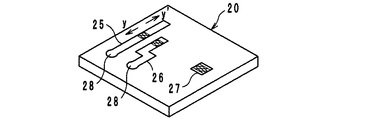
図4に第2実施例であるアイソレータの要部を示す。回路基板20の表面に形成した入力端子電極25及び出力端子電極26のそれぞれがy方向に加えてy’方向にも延在されている。他の構成は前記第1実施例と同様である。
(Refer to the second embodiment, FIG. 4)
FIG. 4 shows a main part of an isolator according to the second embodiment. Each of the
本第2実施例では、入力端子電極25及び出力端子電極26のそれぞれがセルフアライメント効果を発揮する。即ち、リフローはんだ時に溶融したはんだの張力が端子電極25,26のそれぞれで対向するy方向及びy’方向に均衡するのでセルフアライメント効果が大きくなる。
In the second embodiment, each of the
(第3実施例、図5参照)
図5に第3実施例であるアイソレータの要部を示す。回路基板20の表面に形成した入力端子電極25及び出力端子電極26のy方向に延在した部分25a,26aにはんだ流れ防止処理が施されている。具体的には、はんだ濡れ性の悪い材料、樹脂材料を含むオーバーコート材やガラス材料を含むオーバーグレーズ材などで端子電極25,26の一部を被覆している。レーザで端子電極25,26の表面を酸化させてもよい。他の構成は前記第1実施例と同様である。
(Refer to the third embodiment, FIG. 5)
FIG. 5 shows a main part of an isolator according to the third embodiment. Solder flow prevention treatment is applied to the
本第3実施例では、はんだ流れ防止処理によって溶融したはんだがy方向に拡散して張力がy方向に不均衡に増大することはない。特に、はんだが乗る部分がy方向及びy’方向に対称であり、y’方向への端子電極25,26の延在寸法が小さいので、回路基板20上での内部電極のトリミング領域Tを大きくとることができる。
In the third embodiment, the solder melted by the solder flow prevention process does not diffuse in the y direction, and the tension does not increase unbalanced in the y direction. In particular, the portion where the solder is placed is symmetric in the y direction and the y ′ direction, and the extension dimension of the
(第4実施例、図6参照)
図6に第4実施例であるアイソレータの要部を示す。回路基板20の表面に形成した入力端子電極25及び出力端子電極26のy方向に延在した部分が回路基板20に内蔵された電極(図示せず)に接続したビアホール導体28に接続されている。本第4実施例では前記第1実施例で示した終端抵抗Rは回路基板20に内蔵されている。他の構成は第1実施例と同様である。
(Refer to the fourth embodiment, FIG. 6)
FIG. 6 shows a main part of an isolator according to the fourth embodiment. Portions extending in the y direction of the
(第5実施例、図7参照)
図7に第5実施例であるアイソレータを示す。このアイソレータでは、終端抵抗RとコンデンサC1とがチップ型の電子部品として回路基板20の表面に実装されている。それゆえ、出力端子電極26のy方向への延在部分は端部26b,26cに分岐され、回路基板20上には別途端子電極29が形成されている。コンデンサC1は入力端子電極25と出力端子電極26の端部26bとにはんだ付けされる。終端抵抗Rは出力端子電極26の端部26cと端子電極29とにはんだ付けされる。
(Refer to the fifth embodiment, FIG. 7)
FIG. 7 shows an isolator according to a fifth embodiment. In this isolator, a termination resistor R and a capacitor C1 are mounted on the surface of the
また、入力端子電極25及び出力端子電極26はともにy’方向に延在され、フェライト・磁石素子30のリフローはんだ付け時における前記セルフアライメント効果を十分なものとしている。他の構成は前記第1実施例と同様である。
Further, both the
本第5実施例において、入力端子電極25及び出力端子電極26のはんだ付け部分に近い位置にコンデンサC1を配置することが好ましい。配線による残留インダクタンスがアイソレーション特性に与える影響を終端抵抗RとコンデンサC1とで比較すると、終端抵抗RよりもコンデンサC1のほうが大きいからである。つまり、コンデンサC1の残留インダクタンスを小さくしたほうがアイソレーション特性が向上する。
In the fifth embodiment, it is preferable to dispose the capacitor C1 at a position close to the soldered portions of the
(変形例、図8参照)
図8に示すように、永久磁石41の回路基板20との対向面に電極43(車線を付して示す)を形成し、該電極43を回路基板20上に設けた電極とリフローによってはんだ付けしてもよい。電極43が接合される回路基板20上の電極は、入力端子電極25や出力端子電極26であってもよく、あるいは、専用に形成された接続用の電極である。また、前記電極43は接着剤42上にも形成するようにしてもよい。
(Modification, see FIG. 8)
As shown in FIG. 8, an electrode 43 (shown with a lane) is formed on the surface of the
(他の実施例)
なお、本発明に係る非可逆回路素子は前記実施例に限定するものではなく、その要旨の範囲内で種々に変更することができる。
(Other examples)
The non-reciprocal circuit device according to the present invention is not limited to the above-described embodiments, and can be variously modified within the scope of the gist thereof.
例えば、永久磁石41のN極とS極を反転させれば、入力ポートAと出力ポートBが入れ替わる。また、整合用回路は前記実施例(図3参照)に示したもの以外に種々の回路構成を採用することができる。
For example, if the N pole and the S pole of the
また、前記第1及び第2中心電極35,36の形状は種々に変更することができる。例えば、第1中心電極35はフェライト32の主面32a,32b上で2本に分岐していてもよい。また、第2中心電極36は1ターン以上巻回されていればよい。
Further, the shapes of the first and
20…回路基板
25…入力端子電極
26…出力端子電極
27…グランド端子電極
28…ビアホール導体
30…フェライト・磁石素子
32…フェライト
35…第1中心電極
36…第2中心電極
41…永久磁石
43…電極
A…入力ポート
B…出力ポート
C…グランドポート
R…終端抵抗
C1…コンデンサ
DESCRIPTION OF
Claims (6)
前記永久磁石により直流磁界が印加される直方体形状のフェライトと、
前記フェライトの互いに平行に位置する二つの主面に、互いに電気的に絶縁状態で交差して配置された導体膜からなる第1中心電極及び第2中心電極と、
表面に端子電極が形成された回路基板と、
を備え、
前記フェライトの主面に前記永久磁石を固定してフェライト・磁石素子が形成され、該フェライト・磁石素子は前記回路基板上にフェライトの主面が垂直方向に位置するように配置され、
前記回路基板の表面には、第1及び第2中心電極のそれぞれの端部がはんだ付けされる第1、第2及び第3端子電極が形成されており、第1及び第2端子電極は前記フェライトの長辺方向の一端部分に対向して配置され、第3端子電極は前記フェライトの長辺方向の他端部分に対向して配置されており、
第1及び第2端子電極の少なくともいずれかは前記フェライトの長辺方向とほぼ直交する第1の方向に延在され、第1及び第2端子電極の少なくともいずれかは前記第1の方向とはほぼ反対の第2の方向に延在されていること、
を特徴とする非可逆回路素子。 With permanent magnets,
A rectangular parallelepiped ferrite to which a DC magnetic field is applied by the permanent magnet,
A first center electrode and a second center electrode made of a conductor film disposed on two main surfaces of the ferrite that are located in parallel with each other and intersecting each other in an electrically insulated state;
A circuit board having terminal electrodes formed on the surface;
With
A ferrite magnet element is formed by fixing the permanent magnet to the main surface of the ferrite, and the ferrite magnet element is disposed on the circuit board so that the main surface of the ferrite is positioned in a vertical direction.
First, second, and third terminal electrodes are formed on the surface of the circuit board, to which the respective end portions of the first and second center electrodes are soldered. The third terminal electrode is arranged opposite to the other end portion of the ferrite in the long side direction, and is arranged to face one end portion in the long side direction of the ferrite,
At least one of the first and second terminal electrodes extends in a first direction substantially perpendicular to the long side direction of the ferrite, and at least one of the first and second terminal electrodes is the first direction. Extending in a substantially opposite second direction,
A nonreciprocal circuit device characterized by the above.
Priority Applications (1)
| Application Number | Priority Date | Filing Date | Title |
|---|---|---|---|
| JP2008193685A JP5168011B2 (en) | 2008-07-28 | 2008-07-28 | Non-reciprocal circuit element |
Applications Claiming Priority (1)
| Application Number | Priority Date | Filing Date | Title |
|---|---|---|---|
| JP2008193685A JP5168011B2 (en) | 2008-07-28 | 2008-07-28 | Non-reciprocal circuit element |
Publications (2)
| Publication Number | Publication Date |
|---|---|
| JP2010034776A true JP2010034776A (en) | 2010-02-12 |
| JP5168011B2 JP5168011B2 (en) | 2013-03-21 |
Family
ID=41738777
Family Applications (1)
| Application Number | Title | Priority Date | Filing Date |
|---|---|---|---|
| JP2008193685A Expired - Fee Related JP5168011B2 (en) | 2008-07-28 | 2008-07-28 | Non-reciprocal circuit element |
Country Status (1)
| Country | Link |
|---|---|
| JP (1) | JP5168011B2 (en) |
Cited By (2)
| Publication number | Priority date | Publication date | Assignee | Title |
|---|---|---|---|---|
| JP2012222775A (en) * | 2011-04-14 | 2012-11-12 | Murata Mfg Co Ltd | Non-reciprocal circuit element and ferrite-magnet element |
| DE112011100603T5 (en) | 2010-02-19 | 2013-01-31 | Ihi Corp. | Exhaust heat recovery system, energy supply system and exhaust heat recovery process |
Citations (4)
| Publication number | Priority date | Publication date | Assignee | Title |
|---|---|---|---|---|
| JP2003017906A (en) * | 2001-06-28 | 2003-01-17 | Murata Mfg Co Ltd | Irreversible circuit device and communication unit |
| JP2006020052A (en) * | 2004-07-01 | 2006-01-19 | Hitachi Metals Ltd | 2-port isolator |
| JP2006211373A (en) * | 2005-01-28 | 2006-08-10 | Murata Mfg Co Ltd | Two port non-reciprocal circuit element and communication apparatus |
| JP2006311455A (en) * | 2005-05-02 | 2006-11-09 | Murata Mfg Co Ltd | Nonreversible circuit element, manufacturing method thereof and communication unit |
-
2008
- 2008-07-28 JP JP2008193685A patent/JP5168011B2/en not_active Expired - Fee Related
Patent Citations (4)
| Publication number | Priority date | Publication date | Assignee | Title |
|---|---|---|---|---|
| JP2003017906A (en) * | 2001-06-28 | 2003-01-17 | Murata Mfg Co Ltd | Irreversible circuit device and communication unit |
| JP2006020052A (en) * | 2004-07-01 | 2006-01-19 | Hitachi Metals Ltd | 2-port isolator |
| JP2006211373A (en) * | 2005-01-28 | 2006-08-10 | Murata Mfg Co Ltd | Two port non-reciprocal circuit element and communication apparatus |
| JP2006311455A (en) * | 2005-05-02 | 2006-11-09 | Murata Mfg Co Ltd | Nonreversible circuit element, manufacturing method thereof and communication unit |
Cited By (2)
| Publication number | Priority date | Publication date | Assignee | Title |
|---|---|---|---|---|
| DE112011100603T5 (en) | 2010-02-19 | 2013-01-31 | Ihi Corp. | Exhaust heat recovery system, energy supply system and exhaust heat recovery process |
| JP2012222775A (en) * | 2011-04-14 | 2012-11-12 | Murata Mfg Co Ltd | Non-reciprocal circuit element and ferrite-magnet element |
Also Published As
| Publication number | Publication date |
|---|---|
| JP5168011B2 (en) | 2013-03-21 |
Similar Documents
| Publication | Publication Date | Title |
|---|---|---|
| JP4380769B2 (en) | Non-reciprocal circuit device, manufacturing method thereof, and communication device | |
| JP4656186B2 (en) | Non-reciprocal circuit device and method of manufacturing composite electronic component | |
| JP4692679B2 (en) | Non-reciprocal circuit element | |
| JP4640455B2 (en) | Ferrite / magnet elements, non-reciprocal circuit elements and composite electronic components | |
| JP5423814B2 (en) | Circuit module | |
| JP4155342B1 (en) | Non-reciprocal circuit element | |
| JP2007208943A (en) | Nonreciprocal circuit element and communication device | |
| JP4858542B2 (en) | Non-reciprocal circuit element | |
| JP5168011B2 (en) | Non-reciprocal circuit element | |
| JP5056878B2 (en) | Circuit module | |
| JP5573178B2 (en) | Non-reciprocal circuit element | |
| JP5532945B2 (en) | Circuit module | |
| JP2011055222A (en) | Non-reciprocal circuit element | |
| JP5098813B2 (en) | Non-reciprocal circuit device and composite electronic component | |
| JP4760981B2 (en) | Non-reciprocal circuit element | |
| JP5120101B2 (en) | Ferrite / magnet element manufacturing method | |
| JP5083113B2 (en) | Non-reciprocal circuit element | |
| JP2009296051A (en) | Ferrite-magnet element, irreversible circuit element, and composite electronic component | |
| JP4929488B2 (en) | Non-reciprocal circuit element | |
| JP5527331B2 (en) | Circuit module | |
| JP2009290422A (en) | Non-reciprocal circuit element | |
| JP4192883B2 (en) | Two-port nonreciprocal circuit device and communication device | |
| JP4692676B2 (en) | Non-reciprocal circuit element | |
| JP2010157844A (en) | Non-reciprocal circuit element | |
| JP5799794B2 (en) | Non-reciprocal circuit element |
Legal Events
| Date | Code | Title | Description |
|---|---|---|---|
| A621 | Written request for application examination |
Free format text: JAPANESE INTERMEDIATE CODE: A621 Effective date: 20110615 |
|
| A977 | Report on retrieval |
Free format text: JAPANESE INTERMEDIATE CODE: A971007 Effective date: 20120606 |
|
| A131 | Notification of reasons for refusal |
Free format text: JAPANESE INTERMEDIATE CODE: A131 Effective date: 20120612 |
|
| A521 | Request for written amendment filed |
Free format text: JAPANESE INTERMEDIATE CODE: A523 Effective date: 20120727 |
|
| RD02 | Notification of acceptance of power of attorney |
Free format text: JAPANESE INTERMEDIATE CODE: A7422 Effective date: 20120727 |
|
| TRDD | Decision of grant or rejection written | ||
| A01 | Written decision to grant a patent or to grant a registration (utility model) |
Free format text: JAPANESE INTERMEDIATE CODE: A01 Effective date: 20121127 |
|
| A61 | First payment of annual fees (during grant procedure) |
Free format text: JAPANESE INTERMEDIATE CODE: A61 Effective date: 20121210 |
|
| R150 | Certificate of patent or registration of utility model |
Ref document number: 5168011 Country of ref document: JP Free format text: JAPANESE INTERMEDIATE CODE: R150 |
|
| LAPS | Cancellation because of no payment of annual fees |