JP2010034575A - Device for evaluating semiconductor laser - Google Patents
Device for evaluating semiconductor laser Download PDFInfo
- Publication number
- JP2010034575A JP2010034575A JP2009248375A JP2009248375A JP2010034575A JP 2010034575 A JP2010034575 A JP 2010034575A JP 2009248375 A JP2009248375 A JP 2009248375A JP 2009248375 A JP2009248375 A JP 2009248375A JP 2010034575 A JP2010034575 A JP 2010034575A
- Authority
- JP
- Japan
- Prior art keywords
- semiconductor laser
- ground
- conductor plates
- probe
- evaluation apparatus
- Prior art date
- Legal status (The legal status is an assumption and is not a legal conclusion. Google has not performed a legal analysis and makes no representation as to the accuracy of the status listed.)
- Granted
Links
Images


Abstract
Description
この発明は、半導体レーザの高周波特性をチップもしくはサブマウント状態で測定する半導体レーザ評価装置に関するものである。 The present invention relates to a semiconductor laser evaluation apparatus for measuring high-frequency characteristics of a semiconductor laser in a chip or submount state.
光通信分野等で使用される半導体レーザは、高周波変調時の特性評価が必要であるが、一方、デバイスの低価格化に伴うテストコストの削減には、チップ状態での高精度な選別が不可欠である。
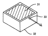
図8は従来の半導体レーザの形状を示す斜視図であり、図において、31は表面に設けられた信号電極、32は裏面にパターニングされた接地電極、33は発光点であり、矢印は発光方向を表している。このような形状を持つ半導体レーザは、信号電極31及び接地電極32が素子の表裏にあるため、両電極間にチップ厚みの分の段差が生じ、高周波でのインピーダンスが取れず、チップ状態では高周波での測定が正確にできない問題があった。
Semiconductor lasers used in the field of optical communications, etc. need to be evaluated at the time of high-frequency modulation. On the other hand, high-precision selection in the chip state is indispensable for reducing test costs associated with lower device costs. It is.
FIG. 8 is a perspective view showing the shape of a conventional semiconductor laser. In the figure, 31 is a signal electrode provided on the front surface, 32 is a ground electrode patterned on the back surface, 33 is a light emitting point, and an arrow is a light emitting direction. Represents. In the semiconductor laser having such a shape, since the
従来の半導体レーザ評価装置は以上のように構成されているので、信号電極と接地電極が同一平面上にない半導体レーザでは、高周波信号源とのインピーダンス整合が取れず、高周波変調時の特性を高精度に測定することができないという問題点があった。 Since the conventional semiconductor laser evaluation apparatus is configured as described above, a semiconductor laser in which the signal electrode and the ground electrode are not on the same plane cannot achieve impedance matching with a high-frequency signal source and has high characteristics during high-frequency modulation. There was a problem that it could not be measured accurately.
この発明は上記のような問題点を解消するためになされたもので、信号電極と接地電極が同一平面上にない半導体レーザであっても、高周波特性を測定することが可能な半導体レーザ評価装置を提供することを目的とする。 The present invention has been made to solve the above problems, and a semiconductor laser evaluation apparatus capable of measuring high-frequency characteristics even in a semiconductor laser in which a signal electrode and a ground electrode are not on the same plane. The purpose is to provide.
この発明の請求項1に係る半導体レーザ評価装置は、接地ステージ上に、同じ高さを有する2つの導体プレートを電気的接触を保って配置するとともに、表面に信号電極かつ裏面に接地電極を設けた所定厚みの半導体レーザを上記2つの導体プレートの間に挟み込むことにより上記半導体レーザの評価を行う半導体レーザ評価装置であって、上記半導体レーザを上記接地ステージ上に載置すると共に上記2つの導体プレートを上記半導体レーザの両側から挟み込んだときには、上記半導体レーザの上面と上記2つの導体プレートの上面とが同一平面上にあるように構成し、上記半導体レーザの信号電極にプローブの信号端子を、上記導体プレートの上面に上記プローブの接地端子を接触させたものである。
In the semiconductor laser evaluation apparatus according to
この発明の請求項2に係る半導体レーザ評価装置は、接地ステージ上に、同じ高さを有する2つの導体プレートを配置するとともに、表面に信号電極かつ裏面に接地電極を設け更に上記裏面に設けられた上記接地電極にサブマウントを接着した所定厚みの半導体レーザを上記2つの導体プレートの間に挟み込むことにより上記半導体レーザの評価を行う半導体レーザ評価装置であって、上記2つの導体プレートの下面に上記サブマウントの厚み分の切り取り部を設け、上記サブマウントを上記接地ステージ上に載置すると共に上記2つの導体プレートを上記サブマウントとの電気的接触を保ちながら上記半導体レーザの両側から挟み込んだときには、上記半導体レーザの上面と上記2つの導体プレートの上面とが同一平面上にあるように構成し、更に上記半導体レーザの信号電極にプローブの信号端子を、上記導体プレートの上面に上記プローブの接地端子を接触させたものである。 According to a second aspect of the present invention, there is provided the semiconductor laser evaluation apparatus according to the present invention, wherein two conductor plates having the same height are arranged on the ground stage, the signal electrode is provided on the front surface, the ground electrode is provided on the back surface, and the back surface is provided. A semiconductor laser evaluation apparatus for evaluating the semiconductor laser by sandwiching a semiconductor laser having a predetermined thickness with a submount bonded to the ground electrode between the two conductor plates, the semiconductor laser evaluation device being formed on a lower surface of the two conductor plates. A cut-out portion corresponding to the thickness of the submount is provided, the submount is placed on the ground stage, and the two conductor plates are sandwiched from both sides of the semiconductor laser while maintaining electrical contact with the submount. Sometimes, the upper surface of the semiconductor laser and the upper surfaces of the two conductor plates are on the same plane. , And further the signal terminals of the probe to the signal electrode of the semiconductor laser, is brought into contact with the ground terminal of the probe to the upper surface of the conductor plate.
この発明によれば、信号電極と接地電極が同一平面上にない半導体レーザであっても、高周波特性を測定することが可能な半導体レーザ評価装置を提供できる。 According to the present invention, it is possible to provide a semiconductor laser evaluation apparatus capable of measuring high-frequency characteristics even with a semiconductor laser in which the signal electrode and the ground electrode are not on the same plane.
実施の形態1.
以下、この発明の一実施形態を図について説明する。図1はこの発明の実施の形態1による高周波特性が測定可能な半導体レーザ評価装置を示す斜視図であり、図において、1は半導体レーザ、1aは半導体レーザ1の発光点、1bは半導体レーザ1の表面に設けられた信号電極、2は接地ステージ、3,4は半導体レーザ1と高精度に同じ厚みを持つよう加工された導体プレートである。導体プレート3,4は、半導体レーザ1を両側から挟み込む形で、接地ステージ2上に電気的接触を保って配置され、更に導体プレート3,4は、半導体レーザ1の発光点の位置精度を合わせる目的も兼ねている。
Hereinafter, an embodiment of the present invention will be described with reference to the drawings. 1 is a perspective view showing a semiconductor laser evaluation apparatus capable of measuring high-frequency characteristics according to
また、半導体レーザ1を両側から挟み込む構造は、半導体レーザ1の裏面光の採光を可能にし、裏面光に対する特性評価を可能にする。
接地ステージ2及び導体プレート3,4は、マイクロ波帯の高周波信号を良好に伝達するため、金などの材質を使用する必要がある。この構造により接地面を導体プレート3,4の上面まで延長することができる。導体プレート3,4は半導体レーザ1と高精度に厚みを同じくしているため、図2に示すように、一般的なGSG(接地―信号−接地)構造やSG構造を持つ高周波プローブによる高周波コンタクトが可能となる。図2において、5は接地―信号−接地構造を持つ高周波プローブである。
In addition, the structure in which the
The
実施の形態2.
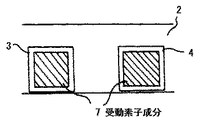
図3はこの発明の実施の形態2による高周波特性が測定可能な半導体レーザ評価装置を示す平面図であり、図において、2は接地ステージ、3,4は導体プレート、6は接地ステージ2上の半導体レーザ配置箇所に埋め込んだ、抵抗,容量,インダクタンス等を持つ受動素子成分である。
受動素子成分6は、半導体レーザの持つインピーダンスを考慮に入れて、高周波信号源とのインピーダンス整合を取るように設計する必要があり、半導体レーザのような抵抗性を示す素子については、抵抗成分を埋め込むことで信号源とのインピーダンス整合を図ることが可能となる。
3 is a plan view showing a semiconductor laser evaluation apparatus capable of measuring high-frequency characteristics according to
The passive element component 6 needs to be designed so as to achieve impedance matching with the high-frequency signal source in consideration of the impedance of the semiconductor laser. By embedding, impedance matching with the signal source can be achieved.
実施の形態3.
図4はこの発明の実施の形態3による高周波特性が測定可能な半導体レーザ評価装置を示す平面図であり、図において、2は接地ステージ、3,4は導体プレート、7は導体プレート3,4上の高周波プローブコンタクト位置に埋め込んだ、抵抗,容量,インダクタンス等を持つ受動素子成分である。
受動素子成分7は、半導体レーザの持つインピーダンスを考慮に入れて、高周波信号源とのインピーダンス整合を取るように設計する必要があり、半導体レーザのような抵抗性を示す素子については、抵抗成分を埋め込むことで信号源とのインピーダンス整合を図ることが可能となる。
4 is a plan view showing a semiconductor laser evaluation apparatus capable of measuring high-frequency characteristics according to
The passive element component 7 needs to be designed so as to obtain impedance matching with the high-frequency signal source in consideration of the impedance of the semiconductor laser. By embedding, impedance matching with the signal source can be achieved.
実施の形態4.
図5はこの発明の実施の形態4による半導体レーザ評価装置にコンタクトを取るための高周波プローブを示す斜視図であり、図において、8は信号源と接続されている高周波ケーブル、9は高周波コネクタ、10はセラミック等からなる誘電体プレート、11,12は接地信号ライン、13は高周波信号ライン、14は信号源と被測定物とのインピーダンス整合を取るための抵抗,容量,インダクタンス等を持つ受動素子成分、15は接地信号ライン11,12及び高周波信号ライン13から被測定物へコンタクトを取るためのプローブ先端部である。
5 is a perspective view showing a high-frequency probe for making contact with a semiconductor laser evaluation apparatus according to
接地信号ライン11,12は高周波コネクタ9の接地部と電気接触を取り、高周波信号ライン13は高周波コネクタ9の中心の信号ラインと電気接触を取る必要がある。又、接地信号ライン11,12及び高周波信号ライン13は金などのマイクロ波帯良導体により構成される必要があり、分布定数を持つ導波路で構成しても良い。
受動素子成分14は、半導体レーザの持つインピーダンスを考慮に入れて、高周波信号源とのインピーダンス整合を取るように設計する必要があり、半導体レーザのような抵抗性を示す素子については、抵抗成分を埋め込むことで、信号源とのインピーダンス整合を図ることが可能となる。
The
The
実施の形態5.
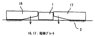
図6はこの発明の実施の形態5による高周波特性が測定可能な半導体レーザ評価装置を示す側面図であり、図において、1は被測定物である半導体レーザ、2は接地ステージ、16,17は下面に切欠きを設けてバネ性を有するようにした導体プレートである。
即ち、導体プレート16,17には、半導体レーザ1の厚みのばらつきを吸収し、接地面と高周波信号面を高精度に同一平面にするための板バネ構造を持つよう加工する。
Embodiment 5 FIG.
FIG. 6 is a side view showing a semiconductor laser evaluation apparatus capable of measuring high-frequency characteristics according to Embodiment 5 of the present invention. In the figure, 1 is a semiconductor laser as a device to be measured, 2 is a grounding stage, 16 and 17 are It is a conductor plate provided with a notch on the lower surface so as to have a spring property.
That is, the
接地ステージ2上の斜線部分は、導体プレート16,17との電気接触を取っている部位を示している。半導体レーザ1及び導体プレート16,17の上面から図示しない高周波プローブにてコンタクトを行った場合、導体プレート16,17がプレート自身の持つバネ性により、半導体レーザ1の上面と高さが同じくなるまで矢印の方向にたわむことで、接地面と信号面の高さを高精度に同じくすることができる。
A hatched portion on the
実施の形態6.
図7はこの発明の実施の形態6による高周波特性が測定可能な半導体レーザ評価装置を示す斜視図であり、図において、1は被測定物である半導体レーザ、2は接地ステージ、18,19は下面に切り取り部が設けられている導体プレート、20は半導体レーザ1を接着しているサブマウント又はブロック等である。
導体プレート18,19は、サブマウント20の厚み分の切り取り部を設け、図7に示されるような斜線部分にてサブマウント20と接地させるようにする。サブマウント20には、導体プレート18,19の斜線部分において接触可能なように、半導体レーザ1の裏面の接地電極と電気的に接触している構造を取る必要がある。
Embodiment 6 FIG.
FIG. 7 is a perspective view showing a semiconductor laser evaluation apparatus capable of measuring high-frequency characteristics according to Embodiment 6 of the present invention. In the figure, 1 is a semiconductor laser as a device to be measured, 2 is a grounding stage, 18 and 19 are A conductor plate 20 having a cut-out portion on the lower surface, 20 is a submount or block to which the
The
導体プレート18,19は、半導体レーザ1と高精度に高さを同じくするよう加工することで、被測定物である半導体レーザ1の接地面と信号面をほぼ同一平面上に配置することができ、GSG構造やSG構造を持つ高周波プローブによる高周波コンタクトが可能となる。
更に、インピーダンス整合を取るためには、上記形態による構造に加えて、実施の形態2〜実施の形態4に示した構造を採用することにより実現する。
The
Furthermore, impedance matching is realized by adopting the structure shown in the second to fourth embodiments in addition to the structure according to the above embodiment.
1 半導体レーザ、2 接地ステージ、
3,4,16,17,18,19 導体プレート、5 プローブ、
6,7,14 受動素子成分、11,12 接地信号ライン、13 高周波信号ライン、20 サブマウント。
1 semiconductor laser, 2 ground stage,
3, 4, 16, 17, 18, 19 Conductor plate, 5 probe,
6, 7, 14 Passive element component, 11, 12 Ground signal line, 13 High-frequency signal line, 20 Submount.
Claims (5)
Priority Applications (1)
| Application Number | Priority Date | Filing Date | Title |
|---|---|---|---|
| JP2009248375A JP4515536B2 (en) | 2009-10-29 | 2009-10-29 | Semiconductor laser evaluation system |
Applications Claiming Priority (1)
| Application Number | Priority Date | Filing Date | Title |
|---|---|---|---|
| JP2009248375A JP4515536B2 (en) | 2009-10-29 | 2009-10-29 | Semiconductor laser evaluation system |
Related Parent Applications (1)
| Application Number | Title | Priority Date | Filing Date |
|---|---|---|---|
| JP00031399A Division JP4416855B2 (en) | 1999-01-05 | 1999-01-05 | Semiconductor laser evaluation system |
Publications (2)
| Publication Number | Publication Date |
|---|---|
| JP2010034575A true JP2010034575A (en) | 2010-02-12 |
| JP4515536B2 JP4515536B2 (en) | 2010-08-04 |
Family
ID=41738616
Family Applications (1)
| Application Number | Title | Priority Date | Filing Date |
|---|---|---|---|
| JP2009248375A Expired - Fee Related JP4515536B2 (en) | 2009-10-29 | 2009-10-29 | Semiconductor laser evaluation system |
Country Status (1)
| Country | Link |
|---|---|
| JP (1) | JP4515536B2 (en) |
Cited By (1)
| Publication number | Priority date | Publication date | Assignee | Title |
|---|---|---|---|---|
| WO2014175014A1 (en) * | 2013-04-25 | 2014-10-30 | 株式会社村田製作所 | Electronic component testing device |
Citations (3)
| Publication number | Priority date | Publication date | Assignee | Title |
|---|---|---|---|---|
| JPH02249288A (en) * | 1989-03-23 | 1990-10-05 | Matsushita Electric Ind Co Ltd | Element fixation jig |
| JPH10125997A (en) * | 1996-10-22 | 1998-05-15 | Matsushita Electric Ind Co Ltd | Semiconductor laser module |
| JP2000028678A (en) * | 1998-07-13 | 2000-01-28 | Mitsubishi Electric Corp | Photosemiconductor chip inspection device and method |
-
2009
- 2009-10-29 JP JP2009248375A patent/JP4515536B2/en not_active Expired - Fee Related
Patent Citations (3)
| Publication number | Priority date | Publication date | Assignee | Title |
|---|---|---|---|---|
| JPH02249288A (en) * | 1989-03-23 | 1990-10-05 | Matsushita Electric Ind Co Ltd | Element fixation jig |
| JPH10125997A (en) * | 1996-10-22 | 1998-05-15 | Matsushita Electric Ind Co Ltd | Semiconductor laser module |
| JP2000028678A (en) * | 1998-07-13 | 2000-01-28 | Mitsubishi Electric Corp | Photosemiconductor chip inspection device and method |
Cited By (3)
| Publication number | Priority date | Publication date | Assignee | Title |
|---|---|---|---|---|
| WO2014175014A1 (en) * | 2013-04-25 | 2014-10-30 | 株式会社村田製作所 | Electronic component testing device |
| JP5987977B2 (en) * | 2013-04-25 | 2016-09-07 | 株式会社村田製作所 | Electronic component testing equipment |
| US10060970B2 (en) | 2013-04-25 | 2018-08-28 | Murata Manufacturing Co., Ltd. | Electronic component testing device |
Also Published As
| Publication number | Publication date |
|---|---|
| JP4515536B2 (en) | 2010-08-04 |
Similar Documents
| Publication | Publication Date | Title |
|---|---|---|
| JP5352170B2 (en) | Inspection socket | |
| KR100864916B1 (en) | Probe for testing a device under test | |
| JP5257088B2 (en) | package | |
| US7173433B2 (en) | Circuit property measurement method | |
| JP2005321305A (en) | Electronic component measurement jig | |
| JP2004170182A (en) | Inspection tool for radio frequency / high-speed device and contact probe | |
| TW200905204A (en) | Probe assembly for probe card | |
| JP2006337361A (en) | Signal probe and probe assembly | |
| KR20140131571A (en) | Flexible cable for low profile electrical device | |
| CN108735678B (en) | Quantum bare chip three-dimensional packaging structure and packaging method thereof | |
| KR20100056733A (en) | A test point structure and the method for radio frequency calibration and radio frequency test on printed curcuit board | |
| JP2016200652A (en) | Connection jig for light modulator | |
| JP4515536B2 (en) | Semiconductor laser evaluation system | |
| JP2001349903A (en) | High frequency probe | |
| KR20170010936A (en) | Radio frequency probe apparatus | |
| JP2010038726A (en) | Probe card | |
| JP2020153947A (en) | Inspection device | |
| JP4416855B2 (en) | Semiconductor laser evaluation system | |
| JP2006214943A (en) | Probe device | |
| JP2008177602A (en) | Apparatus and method for semiconductor laser evaluation | |
| JP4765508B2 (en) | Measuring jig for high frequency devices | |
| JP2007285980A (en) | Probe device | |
| JP2019186729A (en) | Antenna and measuring probe | |
| JP5361023B2 (en) | Method for measuring high-frequency signal transmission characteristics of wiring board and wiring board used therefor | |
| JP6805923B2 (en) | Light modulator |
Legal Events
| Date | Code | Title | Description |
|---|---|---|---|
| TRDD | Decision of grant or rejection written | ||
| A01 | Written decision to grant a patent or to grant a registration (utility model) |
Free format text: JAPANESE INTERMEDIATE CODE: A01 Effective date: 20100427 |
|
| A01 | Written decision to grant a patent or to grant a registration (utility model) |
Free format text: JAPANESE INTERMEDIATE CODE: A01 |
|
| A61 | First payment of annual fees (during grant procedure) |
Free format text: JAPANESE INTERMEDIATE CODE: A61 Effective date: 20100512 |
|
| R150 | Certificate of patent or registration of utility model |
Free format text: JAPANESE INTERMEDIATE CODE: R150 |
|
| FPAY | Renewal fee payment (event date is renewal date of database) |
Free format text: PAYMENT UNTIL: 20130521 Year of fee payment: 3 |
|
| FPAY | Renewal fee payment (event date is renewal date of database) |
Free format text: PAYMENT UNTIL: 20140521 Year of fee payment: 4 |
|
| LAPS | Cancellation because of no payment of annual fees |