JP2010034135A - Field-effect transistor - Google Patents
Field-effect transistor Download PDFInfo
- Publication number
- JP2010034135A JP2010034135A JP2008192183A JP2008192183A JP2010034135A JP 2010034135 A JP2010034135 A JP 2010034135A JP 2008192183 A JP2008192183 A JP 2008192183A JP 2008192183 A JP2008192183 A JP 2008192183A JP 2010034135 A JP2010034135 A JP 2010034135A
- Authority
- JP
- Japan
- Prior art keywords
- electrode
- effect transistor
- field effect
- region
- compound semiconductor
- Prior art date
- Legal status (The legal status is an assumption and is not a legal conclusion. Google has not performed a legal analysis and makes no representation as to the accuracy of the status listed.)
- Granted
Links
Images


Abstract
Description
本発明は、半導体基板に積層された窒化物系III−V族化合物半導体層から横方向へ成長した横方向成長領域を備える電界効果トランジスタに関する。 The present invention relates to a field effect transistor including a laterally grown region grown laterally from a nitride III-V compound semiconductor layer stacked on a semiconductor substrate.
窒化物半導体は、大きな破壊電圧を有し、また、窒化物ヘテロ接合構造は、大きな電流容量を有することが知られている。したがって、高耐圧、大電流を必要とする電力用素子として窒化物系III−V族化合物半導体を活用することが提案されている。 It is known that a nitride semiconductor has a large breakdown voltage, and a nitride heterojunction structure has a large current capacity. Therefore, it has been proposed to use a nitride-based III-V compound semiconductor as a power element that requires a high breakdown voltage and a large current.
AlGaN/GaNへテロ構造を用いた電界効果トランジスタとして、使用面積を最大にして大電流化を実現するために6角形(多角形)の電極配置をしたものが、提案されている(例えば、特許文献1参照)。 As a field effect transistor using an AlGaN / GaN heterostructure, a hexagonal (polygonal) electrode arrangement has been proposed (for example, a patent) in order to maximize the use area and realize a large current. Reference 1).
また、高耐圧の実現には、一般的に横型よりも縦型デバイスが有利であり、縦型構造をした電界効果トランジスタが提案されている(例えば、特許文献2参照)。 In order to achieve a high breakdown voltage, a vertical device is generally more advantageous than a horizontal device, and a field effect transistor having a vertical structure has been proposed (see, for example, Patent Document 2).
したがって、高耐圧・大電流を両立するためには、有効面積を広くした縦型デバイスが有望であると考えられる。また、結晶性を改善するために横方向成長が用いられるが、レイアウトを工夫しないと大電流の半導体装置とする場合には非常に大きなチップ面積が必要になる。 Therefore, in order to achieve both high breakdown voltage and large current, a vertical device with a wide effective area is considered promising. Further, lateral growth is used to improve the crystallinity. However, if the layout is not devised, a very large chip area is required for a high-current semiconductor device.
なお、GaN系半導体の結晶性を改善する方法として、横方向成長を利用するELOG(Epitaxial Lateral Over Growth)成長法(例えば、特許文献3参照)、あるいはPENDEO成長法(例えば、特許文献4参照)といった方法が提案されている。
しかし、従来の窒化物半導体を適用した電界効果トランジスタでは、面積の利用率を高くして、高耐圧で電流容量の大きい縦型構成の電界効果トランジスタとすることが困難であるという問題があった。 However, the conventional field effect transistor using a nitride semiconductor has a problem that it is difficult to increase the area utilization factor and to make a vertical structure field effect transistor with high breakdown voltage and large current capacity. .
本発明はこのような状況に鑑みてなされたものであり、半導体基板に積層された窒化物系III−V族化合物半導体層と、窒化物系III−V族化合物半導体層から積層方向に交差する横方向へ成長した横方向成長領域とを備える電界効果トランジスタであって、横方向成長領域に接触させて形成され通電領域での通電状態を制御する第3電極(ゲート電極)とを備えることにより、積層した窒化物系III−V族化合物半導体層の領域を有効に利用して電流容量および耐電圧を大きくしたノーマリオフの縦型構成の電界効果トランジスタを提供すること目的とする。 The present invention has been made in view of such a situation, and a nitride III-V compound semiconductor layer stacked on a semiconductor substrate and a nitride III-V compound semiconductor layer intersect in the stacking direction. A field effect transistor having a laterally grown region grown in the lateral direction, and a third electrode (gate electrode) that is formed in contact with the laterally grown region and controls an energized state in the energized region. Another object of the present invention is to provide a normally-off vertical field effect transistor in which the current capacity and the withstand voltage are increased by effectively utilizing the region of the laminated nitride III-V compound semiconductor layer.
本発明に係る電界効果トランジスタは、半導体基板と、該半導体基板に積層された窒化物系III−V族化合物半導体層と、該窒化物系III−V族化合物半導体層から積層方向に交差する横方向へ成長した横方向成長領域とを備える電界効果トランジスタであって、前記半導体基板の裏面に形成されオーミック性を有する第1電極と、前記窒化物系III−V族化合物半導体層の表面に形成されオーミック性を有する第2電極と、前記窒化物系III−V族化合物半導体層の積層方向で前記第1電極と前記第2電極との間での電流路となる通電領域と、前記横方向成長領域に接触させて形成され前記通電領域での通電状態を制御する第3電極とを備えることを特徴とする。 A field effect transistor according to the present invention includes a semiconductor substrate, a nitride III-V compound semiconductor layer stacked on the semiconductor substrate, and a lateral crossing from the nitride III-V compound semiconductor layer in the stacking direction. A field effect transistor having a laterally grown region grown in a direction, formed on the back surface of the semiconductor substrate and having ohmic properties, and formed on the surface of the nitride III-V compound semiconductor layer An ohmic second electrode, a current-carrying region serving as a current path between the first electrode and the second electrode in the stacking direction of the nitride-based III-V compound semiconductor layer, and the lateral direction And a third electrode that is formed in contact with the growth region and controls the energization state in the energization region.
この構成により、結晶性の良い横方向成長領域に第3電極を接触させ、第3電極への印加電圧を0ボルトとした状態で通電領域を容易かつ完全に空乏化させることが可能となることから、積層した窒化物系III−V族化合物半導体層の領域を有効に利用して電流容量および耐電圧を大きくした縦型構成の電界効果トランジスタとすることができる。 With this configuration, it is possible to easily and completely deplete the energized region in a state where the third electrode is in contact with the laterally grown region having good crystallinity and the voltage applied to the third electrode is 0 volts. Thus, a field effect transistor having a vertical structure in which the current capacity and the withstand voltage are increased by effectively utilizing the region of the laminated nitride III-V compound semiconductor layer can be obtained.
また、本発明に係る電界効果トランジスタでは、前記横方向成長領域は、前記半導体基板に形成され積層方向での前記窒化物系III−V族化合物半導体層の成長を防止するマスク部に重ねて形成されていることを特徴とする。 In the field effect transistor according to the present invention, the lateral growth region is formed to overlap with a mask portion formed on the semiconductor substrate and preventing the growth of the nitride III-V compound semiconductor layer in the stacking direction. It is characterized by being.
この構成により、結晶性の良い横方向成長領域を容易かつ高精度に形成することが可能となる。 With this configuration, it is possible to easily and accurately form a lateral growth region with good crystallinity.
また、本発明に係る電界効果トランジスタでは、前記第3電極は、前記横方向成長領域の横方向の側面に形成されていることを特徴とする。 In the field effect transistor according to the present invention, the third electrode is formed on a lateral side surface of the lateral growth region.
この構成により、通電領域に対応する横方向成長領域に対して第3電極を配置することが可能となり、第3電極への印加電圧によって容易かつ高精度に通電領域の空乏化を制御することができるので、通電領域の通電状態を容易に制御することが可能な電界効果トランジスタとすることができる。 With this configuration, it is possible to dispose the third electrode in the lateral growth region corresponding to the energized region, and the depletion of the energized region can be controlled easily and with high accuracy by the voltage applied to the third electrode. Therefore, a field effect transistor capable of easily controlling the energization state of the energization region can be obtained.
また、本発明に係る電界効果トランジスタでは、前記第3電極は、前記側面が構成する間隙に埋め込まれていることを特徴とする。 In the field effect transistor according to the present invention, the third electrode is embedded in a gap formed by the side surface.
この構成により、第3電極を容易に形成することが可能となり、生産性、歩留まりおよび信頼性を向上させることができる。 With this configuration, the third electrode can be easily formed, and productivity, yield, and reliability can be improved.
また、本発明に係る電界効果トランジスタでは、前記マスク部は、導電性材料で形成され、前記第3電極は、前記マスク部に接触していることを特徴とする。 In the field effect transistor according to the present invention, the mask portion is made of a conductive material, and the third electrode is in contact with the mask portion.
この構成により、マスク部をベースにして第3電極を形成することが可能となり、第3電極を間隙に容易に埋め込むことが可能となる。 With this configuration, the third electrode can be formed based on the mask portion, and the third electrode can be easily embedded in the gap.
また、本発明に係る電界効果トランジスタでは、前記横方向成長領域は、相互に当接するように形成され、前記第3電極は、相互に当接する前記横方向成長領域の界面に接触していることを特徴とする。 In the field effect transistor according to the present invention, the laterally grown regions are formed to contact each other, and the third electrode is in contact with an interface of the laterally grown regions that are in contact with each other. It is characterized by.
この構成により、第3電極を第2電極と同様に平面的に形成することが可能となるので、第3電極の形成を極めて容易にし、生産性を向上させることができる。 With this configuration, it is possible to form the third electrode in the same plane as the second electrode, so that the formation of the third electrode can be extremely facilitated and productivity can be improved.
また、本発明に係る電界効果トランジスタでは、前記横方向成長領域は、前記半導体基板に形成された溝部の領域で梁状に形成されていることを特徴とする。 In the field effect transistor according to the present invention, the lateral growth region is formed in a beam shape in a region of a groove formed in the semiconductor substrate.
この構成により、結晶性の良い横方向成長領域を容易かつ高精度に形成することが可能となる。 With this configuration, it is possible to easily and accurately form a lateral growth region with good crystallinity.
また、本発明に係る電界効果トランジスタでは、前記横方向成長領域は、相互に当接するように形成され、前記第3電極は、相互に当接する前記横方向成長領域の界面に接触していることを特徴とする。 In the field effect transistor according to the present invention, the laterally grown regions are formed to contact each other, and the third electrode is in contact with an interface of the laterally grown regions that are in contact with each other. It is characterized by.
この構成により、第3電極を第2電極と同様に平面的に形成することが可能となるので、第3電極の形成を極めて容易にし、生産性を向上させることができる。 With this configuration, it is possible to form the third electrode in the same plane as the second electrode, so that the formation of the third electrode can be extremely facilitated and productivity can be improved.
また、本発明に係る電界効果トランジスタでは、前記横方向成長領域は、マグネシウムがドーピングされていることを特徴とする。 In the field effect transistor according to the present invention, the lateral growth region is doped with magnesium.
この構成により、横方向成長領域を介して通電領域にpn接合による空乏層を形成することが可能となり、通電領域の通電状態を容易に制御することができる。 With this configuration, it becomes possible to form a depletion layer by a pn junction in the energization region through the lateral growth region, and the energization state of the energization region can be easily controlled.
また、本発明に係る電界効果トランジスタでは、前記第3電極は、オーミック性を有することを特徴とする。 In the field effect transistor according to the present invention, the third electrode has an ohmic property.
この構成により、横方向成長領域と窒化物系III−V族化合物半導体層とのpn接合による空乏層領域を容易に形成することが可能となり、通電領域の通電状態を容易に制御することができる。 With this configuration, it is possible to easily form a depletion layer region by a pn junction between the laterally grown region and the nitride-based III-V group compound semiconductor layer, and the current-carrying state of the current-carrying region can be easily controlled. .
また、本発明に係る電界効果トランジスタでは、前記第3電極は、前記横方向成長領域に対してショットキー電極としてあることを特徴とする。 In the field effect transistor according to the present invention, the third electrode is a Schottky electrode with respect to the lateral growth region.
この構成により、通電領域にショットキー電極による空乏層を形成することが可能となり、通電領域の通電状態を容易に制御することができる。 With this configuration, it is possible to form a depletion layer by a Schottky electrode in the energization region, and the energization state of the energization region can be easily controlled.
また、本発明に係る電界効果トランジスタでは、前記横方向成長領域は、ストライプ状に配置され、前記第3電極は、前記横方向成長領域に対応させてストライプ状に配置されていることを特徴とする。 In the field effect transistor according to the present invention, the lateral growth region is arranged in a stripe shape, and the third electrode is arranged in a stripe shape corresponding to the lateral growth region. To do.
この構成により、並列構造で面積利用率の高い、大電流化が容易な電界効果トランジスタとすることができる。 With this configuration, a field effect transistor that has a parallel structure, a high area utilization factor, and an easily increased current can be obtained.
また、本発明に係る電界効果トランジスタでは、前記半導体基板は、Si、SiC、または、窒化物系III−V族化合物半導体のいずれか一つを材料としていることを特徴とする。 In the field effect transistor according to the present invention, the semiconductor substrate is made of any one of Si, SiC, and a nitride III-V group compound semiconductor.
この構成により、通電領域を構成する窒化物系III−V族化合物半導体層を容易に形成し、電流容量および耐電圧を大きくすることが可能な電界効果トランジスタとすることができる。 With this configuration, it is possible to easily form a nitride-based III-V compound semiconductor layer that constitutes a current-carrying region, and to obtain a field effect transistor that can increase current capacity and withstand voltage.
本発明に係る電界効果トランジスタによれば、半導体基板と、半導体基板に積層された窒化物系III−V族化合物半導体層と、窒化物系III−V族化合物半導体層から積層方向に交差する横方向へ成長した横方向成長領域とを備える電界効果トランジスタであって、半導体基板の裏面に形成されオーミック性を有する第1電極と、窒化物系III−V族化合物半導体層の表面に形成されオーミック性を有する第2電極と、窒化物系III−V族化合物半導体層の積層方向で第1電極と第2電極との間での電流路となる通電領域と、横方向成長領域に接触させて形成され通電領域での通電状態を制御する第3電極とを備えることから、結晶性の良い横方向成長領域に第3電極を接触させ、第3電極への印加電圧を0ボルトとした状態で通電領域を容易かつ完全に空乏化させることが可能となることから、積層した窒化物系III−V族化合物半導体層の領域を有効に利用して電流容量および耐電圧を大きくした縦型構成の電界効果トランジスタを提供することができるという効果を奏する。 According to the field effect transistor of the present invention, a semiconductor substrate, a nitride III-V compound semiconductor layer stacked on the semiconductor substrate, and a lateral crossing from the nitride III-V compound semiconductor layer in the stacking direction. A field effect transistor having a laterally grown region grown in a direction, the first electrode having ohmic properties formed on a back surface of a semiconductor substrate, and an ohmic formed on the surface of a nitride III-V compound semiconductor layer In contact with the laterally grown region and a current-carrying region serving as a current path between the first electrode and the second electrode in the stacking direction of the nitride-based III-V compound semiconductor layer. And a third electrode that controls the energized state in the energized region, so that the third electrode is brought into contact with the laterally grown region having good crystallinity, and the voltage applied to the third electrode is 0 volts. Energized Since the region can be easily and completely depleted, the electric field having a vertical structure in which the current capacity and the withstand voltage are increased by effectively using the region of the stacked nitride III-V compound semiconductor layer. There is an effect that an effect transistor can be provided.
以下、本発明の実施の形態を図面に基づいて説明する。 Hereinafter, embodiments of the present invention will be described with reference to the drawings.
<実施の形態1>
図1に基づいて、本実施の形態に係る電界効果トランジスタについて説明する。
<
The field effect transistor according to the present embodiment will be described with reference to FIG.
図1は、本発明の実施の形態1に係る電界効果トランジスタの構造および動作状態を示す断面図である。
FIG. 1 is a cross-sectional view showing the structure and operating state of a field effect transistor according to
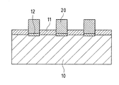
本実施の形態に係る電界効果トランジスタ1は、半導体基板10と、半導体基板10に積層された窒化物系III−V族化合物半導体層20と、窒化物系III−V族化合物半導体層20から積層方向に交差する横方向へ成長した横方向成長領域22とを備える。
The
また、本実施の形態に係る電界効果トランジスタ1は、半導体基板10の裏面に形成されオーミック性を有する第1電極31(ドレイン電極)と、窒化物系III−V族化合物半導体層20の表面に形成されオーミック性を有する第2電極32(ソース電極)と、窒化物系III−V族化合物半導体層20の積層方向で第1電極31と第2電極32との間での電流路となる通電領域21と、横方向成長領域22に接触させて形成され通電領域21での通電状態を制御する第3電極33(ゲート電極)とを備える。
In addition, the
この構成により、結晶性の良い横方向成長領域22に第3電極33を接触させ、第3電極33への印加電圧を0ボルトとした状態で通電領域21を容易かつ完全に空乏化させることが可能となることから、積層した窒化物系III−V族化合物半導体層20の領域を有効に利用して電流容量および耐電圧を大きくした縦型構成の電界効果トランジスタ1とすることができる。
With this configuration, the
つまり、電界効果トランジスタ1は、第3電極33への印加電圧を制御することによって、空乏層領域23を発生させ、空乏層間隔WDDを制御して、電流路としての通電領域21(幅Wp)の通電状態を制御することができる。
That is, the
第3電極33は、横方向成長領域22の導電型によって、オーミック性を持たせる場合と、ショットキー電極とする場合がある。いずれの場合であっても空乏層領域23を形成するように構成される。
The
例えば、横方向成長領域22にマグネシウムをドープしてp型を構成している場合、p型に対するオーミック性を持たせることで、pn接合による空乏層領域23を制御することが可能となる。また、横方向成長領域22がアンドープの場合、ショットキー電極とすることで、空乏層領域23を制御することが可能となる。
For example, when the
本実施の形態では、横方向成長領域22は、半導体基板10に積層して形成され積層方向での窒化物系III−V族化合物半導体層20の成長を防止するマスク部11に重ねて形成されている。したがって、結晶性の良い横方向成長領域22を容易かつ高精度に形成することが可能となる。
In the present embodiment, the
なお、横方向成長領域22は、例えば実施の形態5で示すように、溝部13(図5B、図5C参照)を利用したPENDEO(Pendeo−Epitaxy)成長法を適用して形成することも可能である。
The
また、実施の形態2ないし実施の形態4で示すELOG(Epitaxial Lateral Overgrowth GaN:窒化物半導体を基板上で横方向へ成長させる)成長法、実施の形態5で示すPENDEO成長法などでは、半導体基板10上に形成されたマスク部11(実施の形態2ないし実施の形態4参照)あるいは溝部13(実施の形態5参照)に対して窒化物系III−V族化合物半導体層20の成長方向(積層方向)では、結晶が成長せず、窒化物系III−V族化合物半導体層20から横方向へ結晶が成長し、いわゆる横方向成長が生じる。
Further, in the ELOG (Epitaxial Lateral Over GaN: growing nitride semiconductor laterally on the substrate) growth method shown in the second to fourth embodiments, the PENDEO growth method shown in the fifth embodiment, etc. The growth direction (lamination) of the nitride-based III-V
横方向に伸びた結晶(横方向成長領域22)では大きな結晶欠陥が導入されず、全面に結晶成長した場合よりも結晶性に優れた結晶膜となることが知られている。したがって、本実施の形態では、結晶性に優れた結晶膜を形成することから、制御性および大電流化を有利に進めることができる。 It is known that in the crystal extending in the lateral direction (lateral growth region 22), a large crystal defect is not introduced, and a crystal film having excellent crystallinity is obtained as compared with the case where the crystal is grown on the entire surface. Therefore, in this embodiment, since a crystal film with excellent crystallinity is formed, controllability and increase in current can be advantageously promoted.
本実施の形態では、窒化物系III−V族化合物半導体層20が形成された領域を通電領域21とし、横方向成長領域22に対して第3電極33(ゲート電極)によって、通電領域21に生じる空乏層領域23を制御することによって、通電領域21の電流を制御する。
In the present embodiment, the region where the nitride-based III-V group
また、第3電極33への印加電圧が0Vのときに通電領域21を完全に空乏化することにより、ノーマリオフタイプの電界効果トランジスタ1を実現することが可能である。
Further, when the applied voltage to the
さらに具体的な構成(電界効果トランジスタ1の構造、電界効果トランジスタ1の製造方法、変形例)については実施の形態2以下で詳細を説明する。
Further specific configurations (structure of the
<実施の形態2>
図2Aないし図2Cに基づいて、本実施の形態に係る電界効果トランジスタの製造工程および構造について説明する。なお、基本的な構成は、実施の形態1と同様であるので、符号を援用し、主に異なる事項について説明する。
<Embodiment 2>
The manufacturing process and structure of the field effect transistor according to the present embodiment will be described with reference to FIGS. 2A to 2C. Since the basic configuration is the same as that of the first embodiment, the reference numerals are used to mainly describe different items.
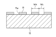
図2Aは、本発明の実施の形態2に係る電界効果トランジスタの製造工程で半導体基板にマスク部を形成した状態の断面を示す断面図である。 FIG. 2A is a cross-sectional view showing a cross-section in a state where a mask portion is formed on a semiconductor substrate in the field-effect transistor manufacturing process according to Embodiment 2 of the present invention.
半導体基板10としてn型GaN基板を用い、マスク部11を形成するためのSiO2膜(0.5μm)を半導体基板10の全面に形成する。SiO2膜は、例えば熱CVD法、プラズマCVD法、あるいはスパッタ法などにより形成することが可能である。
An n-type GaN substrate is used as the
本実施の形態では、ECR(Electron Cyclotron Resonance:電子サイクロトロン共鳴)スパッタを用い、Ar:O2=30:8sccm、スパッタ圧力=0.5Pa、マイクロ波パワー=700W、DCバイアス=600Vで成膜を行なった。 In this embodiment mode, film formation is performed using ECR (Electron Cyclotron Resonance) sputtering, Ar: O 2 = 30: 8 sccm, sputtering pressure = 0.5 Pa, microwave power = 700 W, and DC bias = 600 V. I did it.
次に、フォトリソグラフィ技術を用いてSiO2膜をストライプ状に加工してマスク部11を形成する。なお、マスク部11の幅Wmを3μm、開口部11wの幅Wsを2μmとした。
Next, the
図2Bは、本発明の実施の形態2に係る電界効果トランジスタの製造工程で半導体基板に窒化物系III−V族化合物半導体層(横方向成長領域)を形成した状態の断面を示す断面図である。 FIG. 2B is a cross-sectional view showing a cross section in a state in which a nitride III-V compound semiconductor layer (lateral growth region) is formed on a semiconductor substrate in the manufacturing process of the field effect transistor according to Embodiment 2 of the present invention. is there.
マスク部11を形成した後、MOCVD(有機金属CVD)法を用い、横方向成長に有利な高い基板温度と減圧成長条件を適用して窒化物系III−V族化合物半導体層20を形成(成長)した。窒化物系III−V族化合物半導体層20の縦方向への成長に併せて横方向成長領域22を成長させることが可能である。
After the
なお、横方向成長領域22は、隣接する横方向成長領域22と接触しないで間隙22gを形成するように成長時間を調整した。つまり、横方向成長領域22は、互いに対向する側面22sを構成し、間隙22gは、側面22sによって構成される。
The growth time of the
窒化物系III−V族化合物半導体層20は、具体的にはアンドープのGaNであり、成長条件は、基板温度=1150℃、成長圧力=13kPa、TMG(Tri Methyl Gallium:トリメチルガリウム)流量=200μmol/min、NH3流量=12.5slm(Standard Liter Per Minute)として成膜した。
The nitride-based III-V
なお、縦方向(積層方向)の成長膜厚は、成長条件にも依存するが、2μm程度となった。また、アンドープのGaNのキャリア濃度Ndは、1014cm-3程度となっている。 The growth film thickness in the vertical direction (stacking direction) was about 2 μm although it depends on the growth conditions. The carrier concentration Nd of undoped GaN is about 10 14 cm −3 .
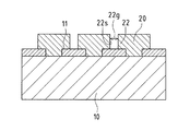
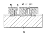
図2Cは、本発明の実施の形態2に係る電界効果トランジスタの製造工程で電極を形成した状態の断面を示す断面図である。 FIG. 2C is a cross-sectional view showing a cross section in a state where electrodes are formed in the manufacturing process of the field effect transistor according to Embodiment 2 of the present invention.
半導体基板10の裏面にオーミック性を有する第1電極31(ドレイン電極)を形成し、窒化物系III−V族化合物半導体層20の表面にオーミック性を有する第2電極32(ソース電極)を形成する。また、横方向成長領域22(側面22s)に接触させて通電領域21での通電状態を制御する第3電極33(ゲート電極)を形成する。
A first electrode 31 (drain electrode) having ohmic properties is formed on the back surface of the
したがって、電界効果トランジスタ1は、第1電極31と第2電極32との間の縦方向(積層方向)で電流を流すことが可能となり、いわゆる縦型トランジスタを構成することとなる。
Therefore, the
また、第3電極33は、横方向成長領域22の横方向の側面22sに形成されている。したがって、通電領域21に対応する横方向成長領域22に対して第3電極33を配置することが可能となり、第3電極33への印加電圧によって容易かつ高精度に通電領域21の空乏化を制御することができるので、通電領域21の通電状態を容易に制御することが可能な電界効果トランジスタ1とすることができる。
The
第1電極31、第2電極32、第3電極33は、メッキ技術を適用して金(Au)を表面にメッキした後、適宜のパターニングによって形成することが可能である。第3電極33は、横方向成長領域22が形成する間隙22gに金を埋め込むことによって形成する。
The
なお、第3電極33は、横方向成長領域22(窒化物系III−V族化合物半導体層20)がアンドープのGaNとされていることから、ショットキー電極として形成されている。
The
ノーマリオフの可否およびピンチオフ電圧は、開口部11wの幅Wsとマスク部11の幅Wm、および、窒化物系III−V族化合物半導体層20のキャリア濃度Ndと第3電極33によって形成される空乏層領域23の空乏層厚Wdとによって決まる。
The normally-off possibility and the pinch-off voltage are defined by the width Ws of the
ショットキー電極(第3電極33)の拡散電位をVdとし、GaN(窒化物系III−V族化合物半導体層20)のキャリア濃度をNdとした場合、空乏層厚Wdは、次の式(1)で求められる。なお式(1)で、εrは窒化物系III−V族化合物半導体層20の比誘電率、ε0は真空の誘電率、qは電子電荷である。
When the diffusion potential of the Schottky electrode (third electrode 33) is Vd and the carrier concentration of GaN (nitride group III-V compound semiconductor layer 20) is Nd, the depletion layer thickness Wd is expressed by the following formula (1 ). In the formula (1), εr is a relative dielectric constant of the nitride III-V
Wd=√((2・εr・ε0/q)(Vd/Nd))・・・(1)
つまり、Vd=1.1V、Nd=1×1014cm-3とした場合、Wd=3.3μm程度となる。
Wd = √ ((2 · εr · ε0 / q) (Vd / Nd)) (1)
That is, when Vd = 1.1 V and Nd = 1 × 10 14 cm −3 , Wd = about 3.3 μm.
したがって、本実施の形態に係る電界効果トランジスタ1では、窒化物系III−V族化合物半導体層20のキャリア濃度Nd=1×1014cm-3、開口部11wの幅Ws=2μm、マスク部11の幅Wm=3μmとした場合、Ws(2μm)+Wm(3μm)=5μmであるから、通電領域21の幅Wpは5μmより小さい状態となっている。
Therefore, in the
つまり、通電領域21の幅Wp(5μm未満)は、空乏層幅Wdの2倍(3.3μm×2=6.6μm)よりも小さいことから、確実にノーマリオフ型とすることが可能となる。つまり、本実施の形態に係る電界効果トランジスタ1は、ピンチオフ電圧0Vのノーマリオフ特性を示すことができる。
That is, since the width Wp (less than 5 μm) of the
なお、キャリア濃度Nd=1×1014cm-3の状態では、開口部11wの幅Ws=3μmとした場合も、ノーマリオフ型となる。しかし、幅Ws=4μmでは、ノーマリオン型となる。
In the state where the carrier concentration Nd = 1 × 10 14 cm −3 , the normally-off type is obtained even when the width Ws of the
また、電流容量(総電流)は、ゲート長(通電領域21の面積)によって決まる。次に電流容量について説明する。 The current capacity (total current) is determined by the gate length (area of the energization region 21). Next, the current capacity will be described.
本実施の形態では、素子の外形面積Sc=1mm×1mmとし、ゲート電極(第3電極33)に対する電極パッド(不図示)の面積などを差し引いて実質上の外形面積Src=0.6mm×0.8mmとした。したがって、トータルゲート長Lg×(幅Wm+幅Ws)=外形面積Srcとなることからトータルゲート長Lgを算出することが可能である。 In the present embodiment, the outer area Sc of the element is set to 1 mm × 1 mm, and the area of the electrode pad (not shown) with respect to the gate electrode (third electrode 33) is subtracted to substantially reduce the outer area Src = 0.6 mm × 0. 8 mm. Therefore, since the total gate length Lg × (width Wm + width Ws) = outer area Src, the total gate length Lg can be calculated.
つまり、トータルゲート長Lgは、トータルゲート長Lg=外形面積Src/(幅Wm+幅Ws)=(0.8mm×0.6mm)/(2μm+3μm)=0.48(mm2)/5(μm)=96mmとして算出される。 That is, the total gate length Lg is as follows: total gate length Lg = outer area Src / (width Wm + width Ws) = (0.8 mm × 0.6 mm) / (2 μm + 3 μm) = 0.48 (mm 2 ) / 5 (μm) = 96 mm.
ゲート電圧2V、ドレイン電圧10Vのときゲート長1μmあたり20μAを流すとすれば、ゲート長1mmでは20mAを流すこととなる。したがって、トータルゲート長Lg=96mmで流せる電流は、(20mA/mm)×96mm=1.92Aとなる。この電流容量は、従来の6角形状の電界効果トランジスタ(実施の形態6参照)の外形面積を等しくした場合に比較して約1.56倍となっていた。 If a gate voltage of 2 V and a drain voltage of 10 V are supplied with 20 μA per 1 μm of gate length, 20 mA is supplied with a gate length of 1 mm. Therefore, the current that can be passed with the total gate length Lg = 96 mm is (20 mA / mm) × 96 mm = 1.92 A. This current capacity was about 1.56 times that of a conventional hexagonal field effect transistor (see Embodiment 6) having the same outer area.
また、素子耐圧としては、600V以上の耐圧を確保することが可能であった。 Further, it was possible to secure a breakdown voltage of 600 V or more as the element breakdown voltage.
上述したとおり、本実施の形態に係る電界効果トランジスタ1では、第3電極33は、横方向成長領域22が互いに対向する側面22sに形成されている。したがって、通電領域21に対応する横方向成長領域22に対して第3電極33を配置することが可能となり、第3電極33への印加電圧によって容易かつ高精度に通電領域21の空乏化を制御することができるので、通電領域21の通電状態を容易に制御することが可能な電界効果トランジスタ1とすることができる。
As described above, in the
また、第3電極33は、側面22sが構成する間隙22gに埋め込まれている。したがって、第3電極33を容易に形成することが可能となり、生産性、歩留まりおよび信頼性を向上させることができる。
The
また、窒化物系III−V族化合物半導体層20の積層方向で第1電極31と第2電極32との間で通電領域21が形成され、第1電極31と第2電極32との間での電流路となる。
In addition, a current-carrying
次に本実施の形態の変形例を説明する。電界効果トランジスタ1の基本的な構成は、上述したとおりであるので、適宜符合を援用して主に異なる事項について説明する。
Next, a modification of the present embodiment will be described. Since the basic configuration of the
半導体基板10としてn型GaN基板10を用い、レジストパターンを幅2μm(開口部11wの幅Wsに対応)、スペース幅3μm(マスク部11の幅Wmに対応)のストライプ状に形成した後、RFスパッタによりAr:O2=16.8:50sccm、スパッタ圧力=0.5Pa、RFパワー=300Wで膜厚0.5μmのWN(窒化タングステン)膜を堆積した。
An n-
レジストパターンを除去してストライプ状のWN膜を形成してマスク部11とした。マスク部11は、マスク部11の幅Wm=3μm、開口部11wの幅Ws=2μmとなっている。
The resist pattern was removed and a striped WN film was formed to form a
次に、MOCVD法を用いて、横方向成長に有利な高い基板温度と減圧成長条件を適用して窒化物系III−V族化合物半導体層20を形成(成長)した。窒化物系III−V族化合物半導体層20は、具体的にはアンドープのGaNであり、成長条件は、基板温度1150℃、成長圧力13kPa、TMG流量=200μmol/min、NH3流量=12.5slmとして成膜した。
Next, a nitride-based III-V group
以下、第1電極31、第2電極32、第3電極33を形成して電界効果トランジスタ1とした。
Hereinafter, the
本変形例に係る電界効果トランジスタ1の形状は、図2Aないし図2Cで記載した電界効果トランジスタ1と同様であり、同様の特性を得ることができた。つまり、本変形例は、マスク部11の材料を変更し、材料の変更に伴い、製造方法を変更したものである。
The shape of the
また、WN膜は、導電性を有する導電性材料である。つまり、本変形例では、マスク部11は、導電性材料で形成され、第3電極33は、マスク部11に接触している。したがって、マスク部11を例えばメッキ電極にして第3電極33を容易に形成することが可能となり、第3電極33を間隙22gに容易に埋め込むことが可能となる。
The WN film is a conductive material having conductivity. That is, in the present modification, the
<実施の形態3>
図3Aないし図3Eに基づいて、本実施の形態に係る電界効果トランジスタの製造工程および構造について説明する。なお、基本的な構成は、実施の形態1、実施の形態2と同様であるので、符号を援用し、主に異なる事項について説明する。
<Embodiment 3>
Based on FIG. 3A thru | or FIG. 3E, the manufacturing process and structure of the field effect transistor which concern on this Embodiment are demonstrated. Since the basic configuration is the same as that of the first and second embodiments, the reference numerals are used and different items are mainly described.
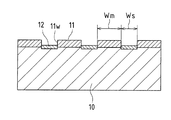
図3Aは、本発明の実施の形態3に係る電界効果トランジスタの製造工程で半導体基板にマスク部およびバッファ層を形成した状態の断面を示す断面図である。 FIG. 3A is a cross-sectional view showing a cross-section in a state where a mask portion and a buffer layer are formed on a semiconductor substrate in the field-effect transistor manufacturing process according to Embodiment 3 of the present invention.
半導体基板10としてn型Si(シリコン)基板を用い、実施の形態2と同様にしてマスク部11(膜厚0.5μmのSiO2膜)を形成してある。なお、本実施の形態では、マスク部11の幅Wmを3μm、開口部11wの幅Wsを1μmとした。
An n-type Si (silicon) substrate is used as the
マスク部11を形成した後、開口部11wを介して露出している半導体基板10にMOCVD法を用いてバッファ層12を形成する。バッファ層12は、例えばAlN(窒化アルミニウム)を200nm成長することによって形成される。
After the
バッファ層12(AlN)の成膜条件は、例えば、基板温度=1150℃、成長圧力=13kPa、TMA(Tri Methyl Aluminium:トリメチルアルミニウム)流量=100μmol/min、NH3流量=12.5slmとした。 The film formation conditions of the buffer layer 12 (AlN) were, for example, a substrate temperature = 1150 ° C., a growth pressure = 13 kPa, a TMA (Trimethyl Aluminum) flow rate = 100 μmol / min, and an NH 3 flow rate = 12.5 slm.
図3Bは、本発明の実施の形態3に係る電界効果トランジスタの製造工程で半導体基板に窒化物系III−V族化合物半導体層を形成する中間状態の断面を示す断面図である。 FIG. 3B is a cross-sectional view showing a cross-section in an intermediate state in which a nitride-based III-V compound semiconductor layer is formed on a semiconductor substrate in the field-effect transistor manufacturing process according to Embodiment 3 of the present invention.
バッファ層12を形成した後、実施の形態2と同様にしてMOCVD法を用い、横方向成長に有利な高い基板温度と減圧成長条件を適用して窒化物系III−V族化合物半導体層20を形成(積層)する。
After the
窒化物系III−V族化合物半導体層20は、具体的にはSiをドープしたGaNであり、成長条件は、基板温度=1150℃、成長圧力=13kPa、TMG流量=200μmol/min、NH3流量=12.5slmとして成膜した。
The nitride III-V
なお、図3Bでは、窒化物系III−V族化合物半導体層20を縦方向(積層方向、成膜方向)に例えば1.5μm成長させた状態を示している。また、Siをドープしていることから、キャリア濃度Nd=1×1015cm-3となった。
FIG. 3B shows a state in which the nitride-based III-V
図3Cは、本発明の実施の形態3に係る電界効果トランジスタの製造工程で半導体基板に窒化物系III−V族化合物半導体層にマグネシウムをドープして横方向成長領域を形成した状態の断面を示す断面図である。 FIG. 3C is a cross-sectional view showing a state in which a lateral growth region is formed by doping a nitride III-V compound semiconductor layer with magnesium in a semiconductor substrate in the manufacturing process of the field effect transistor according to Embodiment 3 of the present invention. It is sectional drawing shown.
図2で、窒化物系III−V族化合物半導体層20を厚さ1.5μm成長させた後、マスク部11相互間に間隙を残している状態で、引き続いてマグネシウム(Mg)をドープしたGaN(キャリア濃度Nd=1×1018cm-3)をSiドープしたGaNの成長時間の1/3の時間成長する。
In FIG. 2, after the nitride-based III-V
MgドープしたGaNは、窒化物系III−V族化合物半導体層20の側面および表面に成長する。窒化物系III−V族化合物半導体層20の側面に成長したGaNは、横方向成長領域22を構成することとなる。
Mg-doped GaN grows on the side surface and the surface of the nitride-based III-V
なお、横方向成長領域22は、相互に隣接する横方向成長領域22が間隙22gを構成する状態で成長を終了される。
The growth in the
図3Dは、本発明の実施の形態3に係る電界効果トランジスタの製造工程で半導体基板に窒化物系III−V族化合物半導体層(横方向成長領域)を形成した状態の断面を示す断面図である。 FIG. 3D is a cross-sectional view showing a cross section in a state in which a nitride III-V compound semiconductor layer (lateral growth region) is formed on a semiconductor substrate in the manufacturing process of the field effect transistor according to the third embodiment of the present invention. is there.
窒化物系III−V族化合物半導体層20の表面に形成されたMgドープのGaNをエッチングする。エッチングは、例えばドライエッチングなどのように方向性を有するエッチング方法を採用する。したがって、窒化物系III−V族化合物半導体層20の表面に成長したGaNは、図3Dに示すように除去され、横方向成長領域22は成長状態を維持する。
The Mg-doped GaN formed on the surface of the nitride III-V
なお、ドライエッチングは、例えば塩素(Cl2)ガスを用いたICP(Inductively Coupled Plasma:誘導結合プラズマ)を適用して行った。 Note that the dry etching was performed by applying ICP (Inductively Coupled Plasma) using, for example, chlorine (Cl 2 ) gas.
図3Eは、本発明の実施の形態3に係る電界効果トランジスタの製造工程で電極を形成した状態の断面を示す断面図である。 FIG. 3E is a sectional view showing a section in a state where electrodes are formed in the manufacturing process of the field effect transistor according to the third embodiment of the present invention.
第1電極31、第2電極32、第3電極33を形成して電界効果トランジスタ1としてある。
The
なお、Si基板(半導体基板10)に対する第1電極31、GaN(窒化物系III−V族化合物半導体層20)に対する第2電極32は、オーミック性を有するオーミック電極とされる。
The
また、第3電極33は、メッキ技術を適用して金などの仕事関数の大きい金属(例えば、Pt、Pd、Auなど)を間隙22gへ埋め込むことによって形成される。仕事関数の大きい金属を適用することから、第3電極33は、MgドープしたGaNに対してオーミック性を持たせることが可能となる。
The
MgドープしたGaN(横方向成長領域22)は、p型となっている。また、SiドープしたGaN(窒化物系III−V族化合物半導体層20)は、n型となっている。したがって、p型に対してオーミック性を有する第3電極33は、横方向成長領域22と窒化物系III−V族化合物半導体層20との間にpn接合を形成して空乏層領域23を生じさせることができる。
Mg-doped GaN (lateral growth region 22) is p-type. Si-doped GaN (nitride-based III-V group compound semiconductor layer 20) is n-type. Therefore, the
つまり、第3電極33は、横方向成長領域22を介して通電領域21にpn接合による空乏層領域23を形成することが可能となり、空乏層厚Wdを制御して通電領域21の通電状態を容易に制御することができる。
That is, the
なお、本実施の形態では、Si基板上にマスク部11としてのSiO2を形成した後にバッファ層12を形成したが、予めSi基板上にAlN、GaNなどをバッファ層12として形成した後にマスク部11としてのSiO2を形成し、その後、窒化物系III−V族化合物半導体層20を形成しても良い。
In the present embodiment, the
また、横方向成長領域22がノンドープGaNであるときは、第3電極33を、横方向成長領域22に対してショットキー電極とすることによって、通電領域21にショットキー電極による空乏層領域23を形成することが可能となり、通電領域21の通電状態を容易に制御することができる。
When the
本実施の形態に係る電界効果トランジスタ1は、ピンチオフ電圧0Vのノーマリオフ特性を示した。
The
本実施の形態でも実施の形態2と同様、素子の外形面積Sc=1mm×1mmとし、ゲート電極(第3電極33)に対する電極パッド(不図示)の面積などを差し引いて実質上の外形面積Src=0.6mm×0.8mmとした。 In the present embodiment, as in the second embodiment, the outer area Sc of the element is set to 1 mm × 1 mm, and the area of the electrode pad (not shown) with respect to the gate electrode (third electrode 33) is subtracted, so that the substantially outer area Src. = 0.6 mm x 0.8 mm.
したがって、トータルゲート長Lgは、トータルゲート長Lg=外形面積Src/(幅Wm+幅Ws)=(0.8mm×0.6mm)/(3μm+1μm)=0.48(mm2)/4(μm)=120mmとなる。 Therefore, the total gate length Lg is as follows: total gate length Lg = outer area Src / (width Wm + width Ws) = (0.8 mm × 0.6 mm) / (3 μm + 1 μm) = 0.48 (mm 2 ) / 4 (μm) = 120 mm.
ゲート電圧2V、ドレイン電圧10Vのときゲート長1μmあたり20μAを流すとすれば、トータルゲート長Lg=120mmで流せる電流は、(20mA/mm)×120mm=2.4Aとなる。この電流容量は、実施の形態2に係る電界効果トランジスタ1に比較してさらに大きな値となっている。
If 20 μA per 1 μm gate length is passed when the gate voltage is 2 V and the drain voltage is 10 V, the current that can be passed with the total gate length Lg = 120 mm is (20 mA / mm) × 120 mm = 2.4 A. This current capacity is larger than that of the
また、素子耐圧としては、600V以上の耐圧を確保することが可能であった。 Further, it was possible to secure a breakdown voltage of 600 V or more as the element breakdown voltage.
上述したとおり、本実施の形態に係る電界効果トランジスタ1では、第3電極33は、側面22sが構成する間隙22gに埋め込まれている。したがって、第3電極33を容易に形成することが可能となり、生産性、歩留まりおよび信頼性を向上させることができる。
As described above, in the
また、第3電極33は、オーミック性を有する構成としてある。したがって、横方向成長領域22と窒化物系III−V族化合物半導体層20とのpn接合による空乏層領域23を容易に形成することが可能となり、通電領域21の通電状態を容易に制御することができる。
Further, the
<実施の形態4>
図4Aおよび図4Bに基づいて、本実施の形態に係る電界効果トランジスタの製造工程および構造について説明する。なお、基本的な構成は、実施の形態1ないし実施の形態3と同様であるので、符号を援用し、主に異なる事項について説明する。
<Embodiment 4>
A manufacturing process and structure of the field effect transistor according to the present embodiment will be described with reference to FIGS. 4A and 4B. Since the basic configuration is the same as that of the first to third embodiments, the reference numerals are used and different items are mainly described.
図4Aは、本発明の実施の形態4に係る電界効果トランジスタの製造工程で半導体基板に窒化物系III−V族化合物半導体層(横方向成長領域)を形成した状態の断面を示す断面図である。 FIG. 4A is a cross-sectional view showing a cross section in a state in which a nitride III-V compound semiconductor layer (lateral growth region) is formed on a semiconductor substrate in the manufacturing process of the field effect transistor according to Embodiment 4 of the present invention. is there.
なお、図4Aは、図3Aないし図3Dに対応する製造工程での処理を施した状態を示している。 FIG. 4A shows a state in which processing in the manufacturing process corresponding to FIGS. 3A to 3D is performed.
先ず、半導体基板10としてn型Si(シリコン)基板を用い、実施の形態2と同様にしてマスク部11(膜厚0.5μmのSiO2膜)を半導体基板10の全面に形成する。
First, an n-type Si (silicon) substrate is used as the
SiO2膜は、半導体基板10がSi基板であることから、熱CVD法、プラズマCVD法などに加えて熱酸化を採用することが可能である。本実施の形態では、ECRスパッタを用い、Ar:O2=30:8sccm、スパッタ圧力=0.5Pa、マイクロ波パワー=700W、DCバイアス=600Vで成膜を行なった。
Since the
次に、フォトリソグラフィ技術を用いてSiO2膜をストライプ状に加工してマスク部11を形成する。なお、本実施の形態では、実施の形態1と同様、マスク部11の幅Wmを3μm、開口部11wの幅Wsを1μmとした。
Next, the
マスク部11を形成した後、MOCVD法を用いて、バッファ層12を形成する。バッファ層12は、例えばAlNを200nm成長することによって形成される。成膜条件は、実施の形態3と同様とすることが可能である。
After the
バッファ層12を形成した後、実施の形態2と同様にしてMOCVD法を用い、横方向成長に有利な高い基板温度と減圧成長条件を適用して窒化物系III−V族化合物半導体層20を形成(積層)する。
After the
窒化物系III−V族化合物半導体層20は、具体的にはSiをドープしたGaNであり、成長条件は、基板温度=1150℃、成長圧力=13kPa、TMG流量=200μmol/min、NH3流量=12.5slmとして成膜した。
The nitride III-V
窒化物系III−V族化合物半導体層20は、縦方向に1.5μm成長させた。また、Siをドープしていることから、キャリア濃度Nd=1×1015cm-3となった。以上の状態は、実施の形態3の図3Aおよび図3Bと同様である。
The nitride III-V
窒化物系III−V族化合物半導体層20を厚さ1.5μm成長させた後、図3Cと同様にして、マスク部11相互間に間隙22gを残している状態で、引き続いてMgドープしたGaN(キャリア濃度Nd=1×1018cm-3)をSiドープしたGaNの成長時間の1/3の時間に加えてさらに横方向成長領域22が相互に当接するまで成長する。
After the nitride-based III-V group
本実施の形態では、横方向成長領域22(側面22s)が相互に当接するように形成されている。つまり、側面22s相互間の間隙22gが消失して横方向成長領域22の界面22bを構成するように横方向成長領域22を成長させている。また、MgドープしたGaNは、図3Cで示したとおり窒化物系III−V族化合物半導体層20の表面にも成長する。
In the present embodiment, the lateral growth regions 22 (side surfaces 22s) are formed so as to contact each other. In other words, the
したがって、窒化物系III−V族化合物半導体層20の表面に形成されたMgドープのGaNをエッチングして除去する。図3Dで示した、窒化物系III−V族化合物半導体層20の表面に形成されたGaNを除去し、横方向成長領域22を残した状態が図4Aの状態である。
Therefore, the Mg-doped GaN formed on the surface of the nitride III-V
図4Bは、本発明の実施の形態4に係る電界効果トランジスタの製造工程で電極を形成した状態の断面を示す断面図である。 FIG. 4B is a sectional view showing a section in a state where electrodes are formed in the manufacturing process of the field effect transistor according to the fourth embodiment of the present invention.
第1電極31、第2電極32、第3電極33を形成して電界効果トランジスタ1としてある。第1電極31、第2電極32は、実施の形態3と同様の形態とすることが可能である。
The
本実施の形態では、第3電極33は、相互に当接する横方向成長領域22の界面22bが窒化物系III−V族化合物半導体層20の表面と交差する端部22tに接触している。つまり、第3電極33は、相互に当接する横方向成長領域22の界面22bに接触している。
In the present embodiment, the
したがって、第3電極33を第2電極32と同様に平面的に形成することが可能となるので、第3電極33の形成を極めて容易にし、生産性を向上させることができる。
Therefore, since the
なお、第3電極33は、横方向成長領域22(MgドープしたGaN)の表面に仕事関数の大きい金属を形成されていることから、オーミック性を有している。オーミック性を有する第3電極33は、横方向成長領域22と窒化物系III−V族化合物半導体層20との間にpn接合を形成して空乏層領域23を生じさせることができる。
The
したがって、空乏層領域23の空乏層厚Wdを制御して通電領域21の通電状態を容易に制御することができる。
Therefore, the energization state of the
また、横方向成長領域22がノンドープGaNであるときは、第3電極33を、横方向成長領域22に対してショットキー電極とすることによって、通電領域21にショットキー電極による空乏層領域23を形成することが可能となり、空乏層厚Wdを制御して通電領域21の通電状態を容易に制御することができる。
When the
本実施の形態に係る電界効果トランジスタ1は、ピンチオフ電圧0Vのノーマリオフ特性を示した。
The
本実施の形態でも実施の形態2と同様、素子の外形面積Sc=1mm×1mmとし、ゲート電極(第3電極33)に対する電極パッド(不図示)の面積などを差し引いて実質上の外形面積Src=0.6mm×0.8mmとした。 In the present embodiment, as in the second embodiment, the outer area Sc of the element is set to 1 mm × 1 mm, and the area of the electrode pad (not shown) with respect to the gate electrode (third electrode 33) is subtracted, so that the substantially outer area Src. = 0.6 mm x 0.8 mm.
したがって、トータルゲート長Lgは、トータルゲート長Lg=外形面積Src/(幅Wm+幅Ws)=(0.8mm×0.6mm)/(3μm+1μm)=0.48(mm2)/4(μm)=120mmとなる。 Therefore, the total gate length Lg is as follows: total gate length Lg = outer area Src / (width Wm + width Ws) = (0.8 mm × 0.6 mm) / (3 μm + 1 μm) = 0.48 (mm 2 ) / 4 (μm) = 120 mm.
つまり、電流容量は、ゲート電圧2V、ドレイン電圧10Vのときゲート長1μmあたり20μAを流すとすれば、実施の形態3と同様、2.4Aとなる。 That is, if the current capacity is 20 μA per 1 μm gate length when the gate voltage is 2 V and the drain voltage is 10 V, the current capacity is 2.4 A as in the third embodiment.
また、素子耐圧としては、600V以上の耐圧を確保することが可能であった。 Further, it was possible to secure a breakdown voltage of 600 V or more as the element breakdown voltage.
<実施の形態5>
図5Aないし図5Dに基づいて、本実施の形態に係る電界効果トランジスタの製造工程および構造について説明する。基本的な構成は、実施の形態1ないし実施の形態4と同様であるので、符号を援用し、主に異なる事項について説明する。なお、実施の形態1ないし実施の形態4では、横方向成長方法として、ELOG成長法を適用したが、本実施の形態では、PENDEO成長法を適用した点が大きく異なる。
<Embodiment 5>
Based on FIG. 5A thru | or FIG. 5D, the manufacturing process and structure of the field effect transistor which concern on this Embodiment are demonstrated. Since the basic configuration is the same as that of the first to fourth embodiments, the reference numerals are used to mainly describe the different items. In the first to fourth embodiments, the ELOG growth method is applied as the lateral growth method. However, the present embodiment is greatly different in that the PENDEO growth method is applied.
図5Aは、本発明の実施の形態5に係る電界効果トランジスタの製造工程で半導体基板にバッファ層および窒化物系III−V族化合物半導体層を形成した状態の断面を示す断面図である。 FIG. 5A is a sectional view showing a section in a state where a buffer layer and a nitride III-V compound semiconductor layer are formed on a semiconductor substrate in the manufacturing process of the field effect transistor according to the fifth embodiment of the present invention.
半導体基板10としてn型SiC基板を用い、半導体基板10にMOCVD法を用いて、バッファ層12を積層し、さらにバッファ層12に窒化物系III−V族化合物半導体層20(図5C参照)の下地となる窒化物系III−V族化合物半導体層20bを積層する。
An n-type SiC substrate is used as the
バッファ層12は、例えばAlNを200nm成長することによって形成される。また、窒化物系III−V族化合物半導体層20bは、GaNを200nm成長することによって形成される。
The
バッファ層12の成膜条件は、例えば、基板温度=1150℃、成長圧力=13kPa、NH3流量=12.5slmとし、AlNを成長するときはTMA流量=100μmol/minとし、GaNを成長するときはTMG流量=100μmol/minとした。
The conditions for forming the
図5Bは、本発明の実施の形態5に係る電界効果トランジスタの製造工程で半導体基板、バッファ層、窒化物系III−V族化合物半導体層に溝部を形成した状態の断面を示す断面図である。 FIG. 5B is a cross-sectional view showing a cross section of the semiconductor substrate, the buffer layer, and the nitride III-V compound semiconductor layer formed with a groove in the manufacturing process of the field effect transistor according to Embodiment 5 of the present invention. .
ストライプ状のレジストパターン13rをレジスト幅3μm(マスク部11の幅Wmに対応)、スペース幅2μm(開口部11wの幅Wsに対応)で形成し、レジストパターン13r(スペース幅2μm、レジスト幅3μm)を形成し、例えばドライエッチングによりGaN(窒化物系III−V族化合物半導体層20b)、AlN(バッファ層12)をエッチングし、さらにSiC基板(半導体基板10)の表面に及ぶ溝部13を形成する。
A stripe-shaped resist
ドライエッチングは、例えば塩素(Cl2)ガスを用いたICPを適用して行った。エッチング条件は、Cl2流量=10sccm、コイルパワー=800W、プレートパワー=35W、圧力=1.3kPaとし、5分間のエッチングを施した。 Dry etching was performed by applying ICP using, for example, chlorine (Cl 2 ) gas. Etching conditions were Cl 2 flow rate = 10 sccm, coil power = 800 W, plate power = 35 W, pressure = 1.3 kPa, and etching was performed for 5 minutes.
窒化物系III−V族化合物半導体層20bの横方向は側面22sを構成し、また、相互に対向する側面22sは、間隙22gを構成する。
The lateral direction of the nitride-based III-V
ドライエッチングの後、レジストパターン13rを除去して次の工程へ移行する。
After the dry etching, the resist
図5Cは、本発明の実施の形態5に係る電界効果トランジスタの製造工程で溝部を形成された下地の窒化物系III−V族化合物半導体層に窒化物系III−V族化合物半導体層をさらに形成した状態の断面を示す断面図である。 FIG. 5C illustrates a nitride III-V compound semiconductor layer further added to the underlying nitride III-V compound semiconductor layer in which a groove is formed in the manufacturing process of the field effect transistor according to Embodiment 5 of the present invention. It is sectional drawing which shows the cross section of the state formed.
溝部13を形成した後、実施の形態2と同様にしてMOCVD法を用い、横方向成長に有利な高い基板温度と減圧成長条件を適用して窒化物系III−V族化合物半導体層20を形成(積層)する。
After forming the
窒化物系III−V族化合物半導体層20は、具体的にはアンドープのGaNであり、成長条件は、基板温度=1150℃、成長圧力=13kPa、TMG流量=100μmol/min、NH3流量=12.5slmとして成膜した。
The nitride-based III-V
本実施の形態では、横方向成長領域22は、半導体基板10に形成された溝部13の領域で梁状に形成されている。したがって、結晶性の良い横方向成長領域22を容易かつ高精度に形成することが可能となる。
In the present embodiment, the
実施の形態4(図4A)の場合と同様、横方向成長領域22の間の間隙22gが消失して界面22bが相互に接触するまで横方向成長領域22(窒化物系III−V族化合物半導体層20)を成長させている。つまり、横方向成長領域22(側面22s)が相互に当接するように形成され、側面22s相互間の間隙22gが消失して横方向成長領域22の界面22bを構成するように横方向成長領域22を成長させている。
As in the case of the fourth embodiment (FIG. 4A), the lateral growth region 22 (nitride-based III-V group compound semiconductor) until the
図5Dは、本発明の実施の形態5に係る電界効果トランジスタの製造工程で電極を形成した状態の断面を示す断面図である。 FIG. 5D is a cross-sectional view showing a cross section in a state where electrodes are formed in the manufacturing process of the field effect transistor according to Embodiment 5 of the present invention.
第1電極31、第2電極32、第3電極33を形成して電界効果トランジスタ1としてある。第1電極31、第2電極32は、実施の形態3と同様の形態とすることが可能である。
The
第3電極33は、実施の形態4と同様の形態とすることが可能である。つまり、第3電極33は、相互に当接する横方向成長領域22の界面22bが窒化物系III−V族化合物半導体層20の表面と交差する端部22tに接触している。つまり、第3電極33は、相互に当接する横方向成長領域22の界面22bに接触している。
The
したがって、第3電極33を第2電極32と同様に平面的に形成することが可能となるので、第3電極33の形成を極めて容易にし、生産性を向上させることができる。
Therefore, since the
第3電極33は、窒化物系III−V族化合物半導体層20、横方向成長領域22をアンドープGaNとしていることから、ショットキー電極として形成している。ショットキー電極としてある第3電極33は、横方向成長領域22(窒化物系III−V族化合物半導体層20)に対して空乏層領域23を生じさせることができる。
The
したがって、空乏層領域23の空乏層厚Wdを制御して通電領域21の通電状態を容易に制御することができる。
Therefore, the energization state of the
また、横方向成長領域22がMgドープしたGaNであるときは、第3電極33を横方向成長領域22に対してオーミック性を持たせることによって、通電領域21にpn接合による空乏層領域23を形成することが可能となり、空乏層厚Wdを制御して通電領域21の通電状態を容易に制御することができる。
Further, when the laterally grown
本実施の形態に係る電界効果トランジスタ1は、ピンチオフ電圧0Vのノーマリオフ特性を示した。
The
本実施の形態でも実施の形態2と同様、素子の外形面積Sc=1mm×1mmとし、ゲート電極(第3電極33)に対する電極パッド(不図示)の面積などを差し引いて実質上の外形面積Src=0.6mm×0.8mmとした。 In the present embodiment, as in the second embodiment, the outer area Sc of the element is set to 1 mm × 1 mm, and the area of the electrode pad (not shown) with respect to the gate electrode (third electrode 33) is subtracted, so that the substantially outer area Src. = 0.6 mm x 0.8 mm.
また、トータルゲート長Lgは、実施の形態2と同様であることから、電流容量は、実施の形態2と同様1.92Aとなる。 Further, since the total gate length Lg is the same as that in the second embodiment, the current capacity is 1.92 A as in the second embodiment.
また、素子耐圧としては、600V以上の耐圧を確保することが可能であった。 Further, it was possible to secure a breakdown voltage of 600 V or more as the element breakdown voltage.
<実施の形態6>
図6に基づいて、実施の形態1ないし実施の形態5に係る電界効果トランジスタの作用、効果について実施の形態6として説明する。
<Embodiment 6>
Based on FIG. 6, the operation and effect of the field effect transistor according to the first to fifth embodiments will be described as a sixth embodiment.
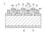
図6は、実施の形態1ないし実施の形態5に係る電界効果トランジスタを適用した本実施の形態に係る電界効果トランジスタの説明図であり、(A)は比較のための従来例に係る電界効果トランジスタの平面図であり、(B)は本実施の形態に係る電界効果トランジスタの平面図である。 FIG. 6 is an explanatory diagram of a field effect transistor according to the present embodiment to which the field effect transistor according to the first to fifth embodiments is applied. FIG. 6A is a field effect according to a conventional example for comparison. It is a top view of a transistor, (B) is a top view of the field effect transistor which concerns on this Embodiment.
従来例に係る電界効果トランジスタ101(図6(A))は、例えば特許文献1に記載された電界効果トランジスタである。中央はソース電極132であり、6角形の領域の背面側はドレイン電極131であり、リング状のゲート電極133がソース電極132とドレイン電極131の間に配置されている。
A field effect transistor 101 (FIG. 6A) according to a conventional example is a field effect transistor described in
電界効果トランジスタ101は、例えば正6角形としてあり、1辺の長さLps=10μmとした場合、正6角形の面積SpはSp=150√3μm2となる。また、ゲート電極133gの直径φは、プロセスマージンを考慮してφ=13μmとすると、ゲート長Lpg=13π=41μmとなる。
The
本実施の形態に係る電界効果トランジスタ1(図6(B))は、ストライプ状に配置されたマスク部11、マスク部11の間に同様に配置された開口部11wを備える。開口部11wに対応してソース電極としての第2電極32が形成され、マスク部11の中央にはゲート電極としての第3電極33(図での理解を容易にするために2点鎖線で表示している。)が形成されている。
The field effect transistor 1 (FIG. 6B) according to the present embodiment includes a
電界効果トランジスタ1では、マスク部11、開口部11wは、ストライプ状に形成される。したがって、横方向成長領域22は、ストライプ状に成長して配置(形成)され、第3電極33は、横方向成長領域22に対応させてストライプ状に配置されている。この構成により、並列構造で面積利用率の高い、大電流化が容易な電界効果トランジスタ1とすることができる。
In the
従来例の正6角形の面積Sp(150√3μm2)と等しい面積(外形面積Src)となる正方形(本実施の形態)の1辺の長さLcは16μmである。 The length Lc of one side of a square (this embodiment) having an area (outside area Src) equal to the area Sp (150√3 μm 2 ) of the regular hexagon of the conventional example is 16 μm.
例えば実施の形態3で示した開口部11wの幅Ws=1μm、マスク部11の幅Wm=3μmの場合Ws+Wm=4μmとなる。実施の形態3の場合を本実施の形態に適用すると、1組のWs+Wm(=4μm)をストライプ状に配置した1個のゲート電極(第3電極33)に対して割り当てるものとする。つまり、1辺の長さLc(16μm)に配置可能なゲート数は、16μm/4μm=4となり、4個のゲートを並列に配置した構成とすることが可能である。また、1個のゲート電極のゲート長Lcgは16μmであるから、全体としてのトータルゲート長Lgは、16μm×4=64μmとなる。
For example, when the width Ws of the
通常の電界効果トランジスタでは、ドレイン電流はトータルゲート長Lgに比例する。したがって、本実施の形態に係る電界効果トランジスタ1と従来例に係る電界効果トランジスタ101とを比べると、同じ面積(150√3μm2)で、ゲート長Lg(64μm)/ゲート長Lpg(41μm)=64/41=1.56と、ゲート長は1.56倍となっているから、ドレイン電流は、1.56倍となる。
In a normal field effect transistor, the drain current is proportional to the total gate length Lg. Therefore, compared to the field-
また、従来例のように多角形を平面上に並置した平面型の電界効果トランジスタ101では、個々のゲート電極133、ソース電極132を相互に接続するためにブリッジ状の配線が必要となる。これに対し、本実施の形態に係る電界効果トランジスタ1では、ゲート電極(第3電極33)、ソース電極(第2電極32)の配置は同一平面内でストライプ状に配置してあることから、相互の接続は同一平面内でゲート配線33w、ソース配線32wによって施すことが可能である。
Further, in the planar
したがって、本実施の形態(つまり、実施の形態1ないし実施の形態5)によれば面積を有効に利用して大電流化および高耐圧化を容易に実現することが可能となる。 Therefore, according to the present embodiment (that is, the first to fifth embodiments), it is possible to easily realize a large current and a high breakdown voltage by effectively using the area.
なお、実施の形態1ないし実施の形態5に係る電界効果トランジスタ1では、半導体基板10は、Si、SiC、または、窒化物系III−V族化合物半導体のいずれか一つを材料としている。したがって、通電領域21を構成する窒化物系III−V族化合物半導体層20を容易に形成し、電流容量および耐電圧を大きくすることが可能な電界効果トランジスタ1とすることができる。
In the
1 電界効果トランジスタ
10 半導体基板
11 マスク部
11w 開口部
12 バッファ層
13 溝部
13r レジストパターン
20 窒化物系III−V族化合物半導体
20b 窒化物系III−V族化合物半導体
21 通電領域
22 横方向成長領域
22b 界面
22g 間隙
22s 側面
22t 端部
23 空乏層領域
31 第1電極
32 第2電極
33 第3電極
WDD 空乏層間隔
Wd 空乏層厚
Wm 幅(マスク部)
Ws 幅(開口部)
Wp 幅(通電領域)
DESCRIPTION OF
Ws width (opening)
Wp width (energized area)
Claims (13)
前記半導体基板の裏面に形成されオーミック性を有する第1電極と、
前記窒化物系III−V族化合物半導体層の表面に形成されオーミック性を有する第2電極と、
前記窒化物系III−V族化合物半導体層の積層方向で前記第1電極と前記第2電極との間での電流路となる通電領域と、
前記横方向成長領域に接触させて形成され前記通電領域での通電状態を制御する第3電極とを備えること
を特徴とする電界効果トランジスタ。 A semiconductor substrate, a nitride III-V compound semiconductor layer stacked on the semiconductor substrate, and a lateral growth region grown laterally from the nitride III-V compound semiconductor layer intersecting the stacking direction A field effect transistor comprising:
A first electrode formed on the back surface of the semiconductor substrate and having ohmic properties;
A second electrode having ohmic properties formed on the surface of the nitride III-V compound semiconductor layer;
A current-carrying region serving as a current path between the first electrode and the second electrode in the stacking direction of the nitride-based III-V compound semiconductor layer;
A field effect transistor comprising: a third electrode that is formed in contact with the laterally grown region and controls an energized state in the energized region.
前記横方向成長領域は、前記半導体基板に形成され積層方向での前記窒化物系III−V族化合物半導体層の成長を防止するマスク部に重ねて形成されていること
を特徴とする電界効果トランジスタ。 The field effect transistor according to claim 1,
The lateral growth region is formed to overlap with a mask portion that is formed on the semiconductor substrate and prevents growth of the nitride III-V compound semiconductor layer in the stacking direction. .
前記第3電極は、前記横方向成長領域の横方向の側面に形成されていること
を特徴とする電界効果トランジスタ。 The field effect transistor according to claim 2, wherein
The field effect transistor, wherein the third electrode is formed on a lateral side surface of the lateral growth region.
前記第3電極は、前記側面が構成する間隙に埋め込まれていること
を特徴とする電界効果トランジスタ。 The field effect transistor according to claim 3,
The field effect transistor, wherein the third electrode is embedded in a gap formed by the side surface.
前記マスク部は、導電性材料で形成され、前記第3電極は、前記マスク部に接触していること
を特徴とする電界効果トランジスタ。 The field effect transistor according to claim 3 or 4, wherein
The field effect transistor, wherein the mask portion is made of a conductive material, and the third electrode is in contact with the mask portion.
前記横方向成長領域は、相互に当接するように形成され、
前記第3電極は、相互に当接する前記横方向成長領域の界面に接触していること
を特徴とする電界効果トランジスタ。 The field effect transistor according to claim 2, wherein
The lateral growth regions are formed to abut one another;
The field effect transistor according to claim 3, wherein the third electrode is in contact with an interface between the laterally grown regions that are in contact with each other.
前記横方向成長領域は、前記半導体基板に形成された溝部の領域で梁状に形成されていること
を特徴とする電界効果トランジスタ。 The field effect transistor according to claim 1,
The lateral growth region is formed in a beam shape in a region of a groove formed in the semiconductor substrate.
前記横方向成長領域は、相互に当接するように形成され、
前記第3電極は、相互に当接する前記横方向成長領域の界面に接触していること
を特徴とする電界効果トランジスタ。 The field effect transistor according to claim 7,
The lateral growth regions are formed to abut one another;
The field effect transistor according to claim 3, wherein the third electrode is in contact with an interface between the laterally grown regions that are in contact with each other.
前記横方向成長領域は、マグネシウムがドーピングされていること
を特徴とする電界効果トランジスタ。 A field effect transistor according to any one of claims 1 to 8, comprising:
2. The field effect transistor according to claim 1, wherein the laterally grown region is doped with magnesium.
前記第3電極は、オーミック性を有すること
を特徴とする電界効果トランジスタ。 The field effect transistor according to claim 9, wherein
The field effect transistor, wherein the third electrode has an ohmic property.
前記第3電極は、前記横方向成長領域に対してショットキー電極としてあること
を特徴とする電界効果トランジスタ。 A field effect transistor according to any one of claims 1 to 8, comprising:
The field effect transistor according to claim 1, wherein the third electrode is a Schottky electrode with respect to the lateral growth region.
前記横方向成長領域は、ストライプ状に配置され、前記第3電極は、前記横方向成長領域に対応させてストライプ状に配置されていること
を特徴とする電界効果トランジスタ。 A field effect transistor according to any one of claims 1 to 11, comprising:
The lateral growth region is arranged in a stripe shape, and the third electrode is arranged in a stripe shape corresponding to the lateral growth region.
前記半導体基板は、Si、SiC、または、窒化物系III−V族化合物半導体のいずれか一つを材料としていること
を特徴とする電界効果トランジスタ。 A field effect transistor according to any one of claims 1 to 12,
The semiconductor substrate is made of any one of Si, SiC, and a nitride III-V compound semiconductor.
Priority Applications (1)
| Application Number | Priority Date | Filing Date | Title |
|---|---|---|---|
| JP2008192183A JP5323412B2 (en) | 2008-07-25 | 2008-07-25 | Field effect transistor |
Applications Claiming Priority (1)
| Application Number | Priority Date | Filing Date | Title |
|---|---|---|---|
| JP2008192183A JP5323412B2 (en) | 2008-07-25 | 2008-07-25 | Field effect transistor |
Publications (2)
| Publication Number | Publication Date |
|---|---|
| JP2010034135A true JP2010034135A (en) | 2010-02-12 |
| JP5323412B2 JP5323412B2 (en) | 2013-10-23 |
Family
ID=41738299
Family Applications (1)
| Application Number | Title | Priority Date | Filing Date |
|---|---|---|---|
| JP2008192183A Expired - Fee Related JP5323412B2 (en) | 2008-07-25 | 2008-07-25 | Field effect transistor |
Country Status (1)
| Country | Link |
|---|---|
| JP (1) | JP5323412B2 (en) |
Cited By (1)
| Publication number | Priority date | Publication date | Assignee | Title |
|---|---|---|---|---|
| WO2018181200A1 (en) * | 2017-03-31 | 2018-10-04 | パナソニックIpマネジメント株式会社 | Semiconductor device |
Citations (6)
| Publication number | Priority date | Publication date | Assignee | Title |
|---|---|---|---|---|
| JP2000232239A (en) * | 1998-12-08 | 2000-08-22 | Nichia Chem Ind Ltd | Growth of nitride semiconductor film and nitride semiconductor element |
| JP2002134735A (en) * | 2000-10-25 | 2002-05-10 | Toshiba Corp | Semiconductor device |
| WO2006093309A1 (en) * | 2005-03-03 | 2006-09-08 | Fuji Electric Holdings Co., Ltd. | Semiconductor device and the method of manufacturing the same |
| JP2006269825A (en) * | 2005-03-24 | 2006-10-05 | Ngk Insulators Ltd | Semiconductor device and manufacturing method thereof |
| JP2007335484A (en) * | 2006-06-13 | 2007-12-27 | Mitsubishi Cable Ind Ltd | Nitride semiconductor wafer |
| JP2008118082A (en) * | 2006-10-11 | 2008-05-22 | New Japan Radio Co Ltd | Nitride semiconductor device and method of manufacturing the same |
-
2008
- 2008-07-25 JP JP2008192183A patent/JP5323412B2/en not_active Expired - Fee Related
Patent Citations (6)
| Publication number | Priority date | Publication date | Assignee | Title |
|---|---|---|---|---|
| JP2000232239A (en) * | 1998-12-08 | 2000-08-22 | Nichia Chem Ind Ltd | Growth of nitride semiconductor film and nitride semiconductor element |
| JP2002134735A (en) * | 2000-10-25 | 2002-05-10 | Toshiba Corp | Semiconductor device |
| WO2006093309A1 (en) * | 2005-03-03 | 2006-09-08 | Fuji Electric Holdings Co., Ltd. | Semiconductor device and the method of manufacturing the same |
| JP2006269825A (en) * | 2005-03-24 | 2006-10-05 | Ngk Insulators Ltd | Semiconductor device and manufacturing method thereof |
| JP2007335484A (en) * | 2006-06-13 | 2007-12-27 | Mitsubishi Cable Ind Ltd | Nitride semiconductor wafer |
| JP2008118082A (en) * | 2006-10-11 | 2008-05-22 | New Japan Radio Co Ltd | Nitride semiconductor device and method of manufacturing the same |
Cited By (1)
| Publication number | Priority date | Publication date | Assignee | Title |
|---|---|---|---|---|
| WO2018181200A1 (en) * | 2017-03-31 | 2018-10-04 | パナソニックIpマネジメント株式会社 | Semiconductor device |
Also Published As
| Publication number | Publication date |
|---|---|
| JP5323412B2 (en) | 2013-10-23 |
Similar Documents
| Publication | Publication Date | Title |
|---|---|---|
| US9685549B2 (en) | Nitride semiconductor device and method for manufacturing same | |
| US8207574B2 (en) | Semiconductor device and method for manufacturing the same | |
| US10020361B2 (en) | Circuit structure having islands between source and drain and circuit formed | |
| US7750369B2 (en) | Nitride semiconductor device | |
| JP4985760B2 (en) | Semiconductor device and manufacturing method thereof | |
| JP4786730B2 (en) | Field effect transistor and manufacturing method thereof | |
| JPWO2003071607A1 (en) | GaN-based field effect transistor | |
| JP4474292B2 (en) | Semiconductor device | |
| JP2011155221A (en) | Semiconductor device and method of manufacturing the same | |
| TW201737395A (en) | Semiconductor device and method for manufacturing the same | |
| KR20210131793A (en) | High Electron Mobility Transistor and method of manufacturing the same | |
| JP6064483B2 (en) | Compound semiconductor device and manufacturing method thereof | |
| CN114402442A (en) | Nitride-based semiconductor device and method for manufacturing the same | |
| JP5379391B2 (en) | Semiconductor device comprising gallium nitride compound semiconductor and method for manufacturing the same | |
| JP2007208037A (en) | Semiconductor device | |
| JP6530210B2 (en) | Semiconductor device and method of manufacturing the same | |
| JP5323412B2 (en) | Field effect transistor | |
| JP2019114581A (en) | Compound semiconductor device and manufacturing method thereof | |
| CN114080691A (en) | Nitride-based semiconductor device and method for manufacturing the same | |
| JP5183857B2 (en) | Field effect transistor and manufacturing method | |
| WO2023181749A1 (en) | Semiconductor device | |
| JP2015153884A (en) | Nitride semiconductor device manufacturing method, nitride semiconductor device, diode and field effect transistor | |
| US11876120B2 (en) | Semiconductor device and method of manufacturing semiconductor device | |
| KR102113253B1 (en) | Nitride based Semiconductor Device | |
| WO2019003363A1 (en) | Semiconductor device and production method therefor |
Legal Events
| Date | Code | Title | Description |
|---|---|---|---|
| A621 | Written request for application examination |
Free format text: JAPANESE INTERMEDIATE CODE: A621 Effective date: 20100826 |
|
| A977 | Report on retrieval |
Free format text: JAPANESE INTERMEDIATE CODE: A971007 Effective date: 20130215 |
|
| A131 | Notification of reasons for refusal |
Free format text: JAPANESE INTERMEDIATE CODE: A131 Effective date: 20130305 |
|
| A521 | Request for written amendment filed |
Free format text: JAPANESE INTERMEDIATE CODE: A523 Effective date: 20130424 |
|
| RD02 | Notification of acceptance of power of attorney |
Free format text: JAPANESE INTERMEDIATE CODE: A7422 Effective date: 20130424 |
|
| A131 | Notification of reasons for refusal |
Free format text: JAPANESE INTERMEDIATE CODE: A131 Effective date: 20130514 |
|
| A521 | Request for written amendment filed |
Free format text: JAPANESE INTERMEDIATE CODE: A523 Effective date: 20130530 |
|
| TRDD | Decision of grant or rejection written | ||
| A01 | Written decision to grant a patent or to grant a registration (utility model) |
Free format text: JAPANESE INTERMEDIATE CODE: A01 Effective date: 20130625 |
|
| A61 | First payment of annual fees (during grant procedure) |
Free format text: JAPANESE INTERMEDIATE CODE: A61 Effective date: 20130717 |
|
| R150 | Certificate of patent or registration of utility model |
Ref document number: 5323412 Country of ref document: JP Free format text: JAPANESE INTERMEDIATE CODE: R150 Free format text: JAPANESE INTERMEDIATE CODE: R150 |
|
| LAPS | Cancellation because of no payment of annual fees |