JP2010020272A - 平面導波技術を利用した波長選択スイッチ - Google Patents
平面導波技術を利用した波長選択スイッチ Download PDFInfo
- Publication number
- JP2010020272A JP2010020272A JP2008286878A JP2008286878A JP2010020272A JP 2010020272 A JP2010020272 A JP 2010020272A JP 2008286878 A JP2008286878 A JP 2008286878A JP 2008286878 A JP2008286878 A JP 2008286878A JP 2010020272 A JP2010020272 A JP 2010020272A
- Authority
- JP
- Japan
- Prior art keywords
- optical
- wavelength
- output
- input
- selective switch
- Prior art date
- Legal status (The legal status is an assumption and is not a legal conclusion. Google has not performed a legal analysis and makes no representation as to the accuracy of the status listed.)
- Granted
Links
- 238000000034 method Methods 0.000 title description 28
- 230000003287 optical effect Effects 0.000 claims abstract description 218
- 239000013307 optical fiber Substances 0.000 claims description 4
- 239000000758 substrate Substances 0.000 claims description 3
- 230000005540 biological transmission Effects 0.000 abstract description 7
- 238000005516 engineering process Methods 0.000 abstract description 5
- 238000004519 manufacturing process Methods 0.000 description 14
- 238000010586 diagram Methods 0.000 description 8
- 229920000642 polymer Polymers 0.000 description 8
- VYPSYNLAJGMNEJ-UHFFFAOYSA-N Silicium dioxide Chemical compound O=[Si]=O VYPSYNLAJGMNEJ-UHFFFAOYSA-N 0.000 description 4
- 230000007547 defect Effects 0.000 description 3
- 238000007796 conventional method Methods 0.000 description 2
- 239000000377 silicon dioxide Substances 0.000 description 2
- XUIMIQQOPSSXEZ-UHFFFAOYSA-N Silicon Chemical compound [Si] XUIMIQQOPSSXEZ-UHFFFAOYSA-N 0.000 description 1
- 238000004891 communication Methods 0.000 description 1
- 238000004049 embossing Methods 0.000 description 1
- 238000003780 insertion Methods 0.000 description 1
- 230000037431 insertion Effects 0.000 description 1
- 230000010354 integration Effects 0.000 description 1
- 238000012986 modification Methods 0.000 description 1
- 230000004048 modification Effects 0.000 description 1
- 239000004065 semiconductor Substances 0.000 description 1
- 229910052710 silicon Inorganic materials 0.000 description 1
- 239000010703 silicon Substances 0.000 description 1
- 229910052814 silicon oxide Inorganic materials 0.000 description 1
- 239000010409 thin film Substances 0.000 description 1
Images


Classifications
-
- H—ELECTRICITY
- H04—ELECTRIC COMMUNICATION TECHNIQUE
- H04Q—SELECTING
- H04Q11/00—Selecting arrangements for multiplex systems
- H04Q11/0001—Selecting arrangements for multiplex systems using optical switching
- H04Q11/0005—Switch and router aspects
-
- H—ELECTRICITY
- H04—ELECTRIC COMMUNICATION TECHNIQUE
- H04Q—SELECTING
- H04Q11/00—Selecting arrangements for multiplex systems
- H04Q11/0001—Selecting arrangements for multiplex systems using optical switching
- H04Q11/0005—Switch and router aspects
- H04Q2011/0007—Construction
- H04Q2011/0016—Construction using wavelength multiplexing or demultiplexing
-
- H—ELECTRICITY
- H04—ELECTRIC COMMUNICATION TECHNIQUE
- H04Q—SELECTING
- H04Q11/00—Selecting arrangements for multiplex systems
- H04Q11/0001—Selecting arrangements for multiplex systems using optical switching
- H04Q11/0005—Switch and router aspects
- H04Q2011/0007—Construction
- H04Q2011/0035—Construction using miscellaneous components, e.g. circulator, polarisation, acousto/thermo optical
-
- H—ELECTRICITY
- H04—ELECTRIC COMMUNICATION TECHNIQUE
- H04Q—SELECTING
- H04Q11/00—Selecting arrangements for multiplex systems
- H04Q11/0001—Selecting arrangements for multiplex systems using optical switching
- H04Q11/0005—Switch and router aspects
- H04Q2011/0052—Interconnection of switches
Landscapes
- Engineering & Computer Science (AREA)
- Computer Networks & Wireless Communication (AREA)
- Optical Modulation, Optical Deflection, Nonlinear Optics, Optical Demodulation, Optical Logic Elements (AREA)
- Optical Integrated Circuits (AREA)
Abstract
【解決手段】本発明による波長選択スイッチは、M個の波長チャンネルの光信号の入力を受けて各波長チャンネル別に分離して光伝送線路に出力する第1波長分割多重化器と、前記第1波長分割多重化器から前記M個の波長チャンネル別に出力された光信号の経路をN個の出力ポートのうち何れか一つの出力ポートに変更する前記M個の光スイッチと、前記光スイッチの前記N個の出力ポートのうち一つずつ連結され、前記N個の入力された光信号を結合して出力する(M+N−1)個の光結合器と、前記(M+N−1)個の入力ポート及び前記N個の出力ポートを有し、前記(M+N−1)個の前記光結合器の出力信号が各々前記入力ポートに連結され、前記入力された信号を多重化させて前記N個の出力ポートに出力する第2波長分割多重化器とを含む。
【選択図】図2
Description
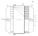
110、140、210、240、340、342 波長分割多重化器
111 入力ポート
120、220、320、322スイッチアレイ
121〜12N、321 光スイッチ
121_1〜121_8 ポリマーTIR光スイッチ
131〜13K 光結合器
140、240第2波長分割多重化器
141 出力ポート
142、144 スラブ導波路
143 配列導波路
Claims (10)
- M(前記Mは、1より大きい整数)個の波長チャンネルの光信号の入力を受けて各波長チャンネル別に分離して出力する第1波長分割多重化器と、
前記第1波長分割多重化器から前記M個の波長チャンネル別に出力された光信号の経路をN(前記Nは、1より大きく前記Mより小さいか等しい整数)個の出力ポートのうち何れか一つの出力ポートに変更する前記M個の光スイッチと、
前記光スイッチの前記N個の出力ポートに各々連結され、前記N個の入力された光信号を結合して出力する(M+N−1)個の光結合器と、
前記(M+N−1)個の入力ポート及び前記N個の出力ポートを有し、前記(M+N−1)個の前記光結合器の出力信号が各々前記入力ポートに連結され、前記入力された信号を多重化させて前記N個の出力ポートに出力する第2波長分割多重化器と
を含むことを特徴とする波長選択スイッチ。 - 前記光スイッチのうちI(前記Iは、1より大きく前記Mより小さい整数)番目光スイッチのJ(前記Jは、1より大きく前記Nより小さい整数)番目出力ポートは、(I+J−1)番目光結合器の入力ポートのうち何れか一つと連結されることを特徴とする請求項1に記載の波長選択スイッチ。
- 前記波長選択スイッチは、前記第1波長分割多重化器及び前記光スイッチの間に連結され、前記チャンネル別光信号パワーを調節する可変光減衰器或いは光増幅器をさらに含むことを特徴とする請求項1に記載の波長選択スイッチ。
- 前記第1及び第2波長分割多重化器は、配列導波路波長分割多重化器で具現されることを特徴とする請求項1に記載の波長選択スイッチ。
- 前記第1及び第2波長分割多重化器は、反射型回折格子波長分割多重化器に具現されることを特徴とする請求項1に記載の波長選択スイッチ。
- 前記光スイッチには、各々入力ポート及び出力ポートが一つずつ追加され、
追加された前記入力ポート及び前記出力ポートを利用して複数の波長選択スイッチが連結されることによって前記N個よりも多い出力を提供されることを特徴とする請求項1に記載の波長選択スイッチ。 - 前記波長選択スイッチは、一つの平面基板に単一集積光素子で具現されることを特徴とする請求項1に記載の波長選択スイッチ。
- 前記波長選択スイッチに利用される光素子は、各々光ファイバーを利用して連結されることを特徴とする請求項1に記載の波長選択スイッチ。
- M(前記Mは、1より大きい整数)個の波長チャンネルの光信号の入力を受けて各波長チャンネル別に分離して出力する第1波長分割多重化器と、
前記第1波長分割多重化器から前記M個の波長チャンネル別に出力された光信号の経路をN(前記Nは、1より大きく前記Mより小さいか等しい整数)個の出力ポートのうち何れか一つの出力ポートに変更する前記M個の光スイッチと、
前記光スイッチと連結され、(N*(M−1)+(N−1)*(N−1)+1)個の入力チャンネル及び前記N個の出力チャンネルを有し、前記入力チャンネルの間の波長間隔は、前記光信号のチャンネル波長の1/Nであり、前記出力チャンネルの間の波長間隔は、前記光信号のチャンネル波長の1/(N−1)である第2波長分割多重化器と
を含むことを特徴とする波長選択スイッチ。 - 前記光スイッチのうちI(前記Iは、1より大きく前記Mより小さい整数)番目光スイッチのJ(前記Jは、1より大きく前記Nより小さい整数)番目出力ポートは、前記第2波長分割多重化器の(N*(I−1)+(N−1)*(J−1)+1)番目入力ポートに連結されることを特徴とする波長選択スイッチ。
Applications Claiming Priority (2)
| Application Number | Priority Date | Filing Date | Title |
|---|---|---|---|
| KR10-2008-0066470 | 2008-07-09 | ||
| KR1020080066470A KR100960919B1 (ko) | 2008-07-09 | 2008-07-09 | 평면도파 기술을 이용한 파장선택 스위치 |
Publications (2)
| Publication Number | Publication Date |
|---|---|
| JP2010020272A true JP2010020272A (ja) | 2010-01-28 |
| JP4719786B2 JP4719786B2 (ja) | 2011-07-06 |
Family
ID=41505268
Family Applications (1)
| Application Number | Title | Priority Date | Filing Date |
|---|---|---|---|
| JP2008286878A Expired - Fee Related JP4719786B2 (ja) | 2008-07-09 | 2008-11-07 | 平面導波技術を利用した波長選択スイッチ |
Country Status (3)
| Country | Link |
|---|---|
| US (1) | US20100008670A1 (ja) |
| JP (1) | JP4719786B2 (ja) |
| KR (1) | KR100960919B1 (ja) |
Cited By (1)
| Publication number | Priority date | Publication date | Assignee | Title |
|---|---|---|---|---|
| JP2012242677A (ja) * | 2011-05-20 | 2012-12-10 | Nippon Telegr & Teleph Corp <Ntt> | 光回路と、この光回路を用いた光増幅器、可変分散補償器、および可変光遅延器 |
Families Citing this family (3)
| Publication number | Priority date | Publication date | Assignee | Title |
|---|---|---|---|---|
| KR101433856B1 (ko) | 2010-07-21 | 2014-08-27 | 한국전자통신연구원 | 광 스위치 소자 및 그의 제조방법 |
| KR102302604B1 (ko) | 2017-11-01 | 2021-09-16 | 한국전자통신연구원 | 분광 장치 |
| CN112987186B (zh) * | 2021-04-02 | 2025-01-17 | 上海邮电设计咨询研究院有限公司 | 一种支持光复用段保护功能的光交叉线路器件 |
Citations (2)
| Publication number | Priority date | Publication date | Assignee | Title |
|---|---|---|---|---|
| JPH08237221A (ja) * | 1995-02-27 | 1996-09-13 | Nippon Telegr & Teleph Corp <Ntt> | 波長分割型光通話路 |
| JP2007148042A (ja) * | 2005-11-28 | 2007-06-14 | Nippon Telegr & Teleph Corp <Ntt> | 波長選択光スイッチ、光合流器、光分岐器および波長選択光スイッチモジュール |
Family Cites Families (6)
| Publication number | Priority date | Publication date | Assignee | Title |
|---|---|---|---|---|
| US5742416A (en) * | 1996-03-28 | 1998-04-21 | Ciena Corp. | Bidirectional WDM optical communication systems with bidirectional optical amplifiers |
| US6493119B1 (en) * | 1999-09-07 | 2002-12-10 | Chien-Yu Kuo | Scalable DWDM network switch architecture with wavelength tunable sources |
| JP4209080B2 (ja) * | 2000-11-29 | 2009-01-14 | 富士通株式会社 | 光クロスコネクト装置及び該装置を有するシステム |
| JP3976602B2 (ja) * | 2002-03-28 | 2007-09-19 | 富士通株式会社 | 光クロスコネクト装置 |
| KR100438437B1 (ko) * | 2002-04-10 | 2004-07-03 | 삼성전자주식회사 | 광 통신망에서 광회선분배장치 및 그 처리 방법 |
| JP4489678B2 (ja) * | 2005-09-30 | 2010-06-23 | 富士通株式会社 | 波長選択光スイッチおよび分光機能を備えた光デバイス |
-
2008
- 2008-07-09 KR KR1020080066470A patent/KR100960919B1/ko not_active Expired - Fee Related
- 2008-11-07 JP JP2008286878A patent/JP4719786B2/ja not_active Expired - Fee Related
- 2008-11-21 US US12/275,553 patent/US20100008670A1/en not_active Abandoned
Patent Citations (2)
| Publication number | Priority date | Publication date | Assignee | Title |
|---|---|---|---|---|
| JPH08237221A (ja) * | 1995-02-27 | 1996-09-13 | Nippon Telegr & Teleph Corp <Ntt> | 波長分割型光通話路 |
| JP2007148042A (ja) * | 2005-11-28 | 2007-06-14 | Nippon Telegr & Teleph Corp <Ntt> | 波長選択光スイッチ、光合流器、光分岐器および波長選択光スイッチモジュール |
Non-Patent Citations (1)
| Title |
|---|
| JPN6010067501, S. Kakehashi, et al., ""Performance of waveband MUX/DEMUX using concatenated AWGs"", IEEE Photonics Technology Letters, 200708, Vol. 19, No. 16, p.1197−1199 * |
Cited By (1)
| Publication number | Priority date | Publication date | Assignee | Title |
|---|---|---|---|---|
| JP2012242677A (ja) * | 2011-05-20 | 2012-12-10 | Nippon Telegr & Teleph Corp <Ntt> | 光回路と、この光回路を用いた光増幅器、可変分散補償器、および可変光遅延器 |
Also Published As
| Publication number | Publication date |
|---|---|
| KR20100006293A (ko) | 2010-01-19 |
| KR100960919B1 (ko) | 2010-06-04 |
| US20100008670A1 (en) | 2010-01-14 |
| JP4719786B2 (ja) | 2011-07-06 |
Similar Documents
| Publication | Publication Date | Title |
|---|---|---|
| US20020003643A1 (en) | Multi-channel wavelength slicing using an etalon-based interleaver for dense wavelength division multiplexing | |
| WO2006035520A1 (ja) | 光挿入分岐装置及び光ネットワークシステム | |
| JP4739928B2 (ja) | 波長選択光スイッチおよび波長選択光スイッチモジュール | |
| JP5128254B2 (ja) | 波長選択スイッチ | |
| JP4864771B2 (ja) | 光信号モニタ装置、光システム及び光信号モニタ方法 | |
| JP4719786B2 (ja) | 平面導波技術を利用した波長選択スイッチ | |
| US6597841B1 (en) | Multi-output arrayed waveguide grating demultiplexer | |
| JP4748524B2 (ja) | アレイ導波路格子型合分波器 | |
| JP4916489B2 (ja) | 光回路 | |
| KR100474695B1 (ko) | 파장분할다중 광통신망을 위한 양방향 광 분기/결합다중화기 | |
| US7257285B2 (en) | Wavelength-selective switch and integrated wavelength demultiplexer using stacked planar lightwave circuits | |
| US6993217B2 (en) | Optical switch device | |
| US7298976B2 (en) | Bi-directional optical cross-connect device | |
| JP2003315570A (ja) | 光波長合分波器 | |
| Nakamura et al. | 1× 2 silicon wavelength selective switch using fold back arrayed-waveguide gratings | |
| JP5164153B2 (ja) | 光波長群クロスコネクト装置 | |
| KR100965842B1 (ko) | 다채널 광분기결합 멀티플렉서 | |
| JP4168778B2 (ja) | 光機能装置 | |
| KR100547780B1 (ko) | 순환기와 반사기를 이용한 광 분기/결합기 | |
| US20040218926A1 (en) | Optical add/drop multiplexer | |
| JP2007155777A (ja) | モニタ回路 | |
| EP1122905A2 (en) | Apparatus and method for wavelength multiplexing/demultiplexing | |
| JP4366955B2 (ja) | 光機能装置および光機能モジュール | |
| JP2010117626A (ja) | アレイ導波路型回折格子及びこれを備える光合波装置 | |
| JP4899822B2 (ja) | 光合分波器 |
Legal Events
| Date | Code | Title | Description |
|---|---|---|---|
| A977 | Report on retrieval |
Free format text: JAPANESE INTERMEDIATE CODE: A971007 Effective date: 20101115 |
|
| A131 | Notification of reasons for refusal |
Free format text: JAPANESE INTERMEDIATE CODE: A131 Effective date: 20101126 |
|
| A521 | Written amendment |
Free format text: JAPANESE INTERMEDIATE CODE: A523 Effective date: 20110216 |
|
| A01 | Written decision to grant a patent or to grant a registration (utility model) |
Free format text: JAPANESE INTERMEDIATE CODE: A01 Effective date: 20110304 |
|
| A61 | First payment of annual fees (during grant procedure) |
Free format text: JAPANESE INTERMEDIATE CODE: A61 Effective date: 20110404 |
|
| R150 | Certificate of patent or registration of utility model |
Free format text: JAPANESE INTERMEDIATE CODE: R150 |
|
| FPAY | Renewal fee payment (event date is renewal date of database) |
Free format text: PAYMENT UNTIL: 20140408 Year of fee payment: 3 |
|
| R250 | Receipt of annual fees |
Free format text: JAPANESE INTERMEDIATE CODE: R250 |
|
| LAPS | Cancellation because of no payment of annual fees |