JP2010004248A - 差動伝送線路 - Google Patents
差動伝送線路 Download PDFInfo
- Publication number
- JP2010004248A JP2010004248A JP2008160446A JP2008160446A JP2010004248A JP 2010004248 A JP2010004248 A JP 2010004248A JP 2008160446 A JP2008160446 A JP 2008160446A JP 2008160446 A JP2008160446 A JP 2008160446A JP 2010004248 A JP2010004248 A JP 2010004248A
- Authority
- JP
- Japan
- Prior art keywords
- transmission line
- signal
- conductor
- differential transmission
- ground conductor
- Prior art date
- Legal status (The legal status is an assumption and is not a legal conclusion. Google has not performed a legal analysis and makes no representation as to the accuracy of the status listed.)
- Granted
Links
Images


Classifications
-
- H—ELECTRICITY
- H01—ELECTRIC ELEMENTS
- H01P—WAVEGUIDES; RESONATORS, LINES, OR OTHER DEVICES OF THE WAVEGUIDE TYPE
- H01P3/00—Waveguides; Transmission lines of the waveguide type
- H01P3/02—Waveguides; Transmission lines of the waveguide type with two longitudinal conductors
-
- H—ELECTRICITY
- H01—ELECTRIC ELEMENTS
- H01P—WAVEGUIDES; RESONATORS, LINES, OR OTHER DEVICES OF THE WAVEGUIDE TYPE
- H01P3/00—Waveguides; Transmission lines of the waveguide type
- H01P3/02—Waveguides; Transmission lines of the waveguide type with two longitudinal conductors
- H01P3/026—Coplanar striplines [CPS]
-
- H—ELECTRICITY
- H01—ELECTRIC ELEMENTS
- H01P—WAVEGUIDES; RESONATORS, LINES, OR OTHER DEVICES OF THE WAVEGUIDE TYPE
- H01P1/00—Auxiliary devices
- H01P1/02—Bends; Corners; Twists
Landscapes
- Structure Of Printed Boards (AREA)
- Waveguides (AREA)
Abstract
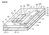
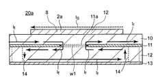
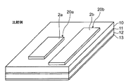
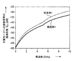
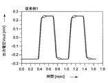
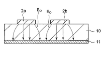
【解決手段】差動伝送線路は、互いに実質的に平行なおもて面と裏面を有する平行平板の誘電体基板10と、誘電体基板10の裏面上に形成された接地導体11と、接地導体11上に形成された誘電体層12と、誘電体層12上に形成された接地導体13と、誘電体基板10のおもて面上に互いに平行となるように形成された1対の信号導体2a,2bとを備えて構成される。信号導体2aと接地導体11,13とにより第1の伝送線路であるマイクロストリップ線路20aを構成し、信号導体2bと接地導体11,13とにより第2の伝送線路であるマイクロストリップ線路20bを構成する。接地導体11において、信号導体2a,2bの長手方向に対して実質的に直交しかつ立体的に交差するようにスロット11a,11bが形成される。
【選択図】図1
Description
互いに実質的に平行な第1の面と第2の面を有する基板と、
上記基板の第2の面上に形成された第1の接地導体と、
上記第1の接地導体上に形成された誘電体層と、
上記誘電体層上に形成された第2の接地導体と、
上記基板の第1の面上に互いに平行となるように形成された第1と第2の信号導体とを備え、
上記第1の信号導体と上記第1及び第2の接地導体とにより第1の伝送線路を構成し、上記第2の信号導体と上記第1及び第2の接地導体とにより第2の伝送線路を構成する差動伝送線路であって、
上記第1の接地導体において、上記第1と第2の信号導体の長手方向に対して実質的に直交しかつ立体的に交差するように形成されたスロットと、
上記第1の接地導体と上記第2の接地導体とを接続する接続導体とを備えたことを特徴とする。
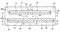
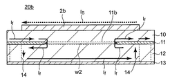
まず、図1乃至図4を参照して本発明の一実施形態に係る差動伝送線路について以下に説明する。図1は本発明の一実施形態に係る差動伝送線路の斜視図であり、図2は図1の差動伝送線路の上面図である。
|w1−w2|≧|L1−L2|
|w1−w2|≧|L1−L2|
10…誘電体基板、
11,13…接地導体、
11a,11b…スロット、
11c…屈曲部、
12…誘電体層、
14…ビア導体、
20a,20b…マイクロストリップ線路、
Is…信号電流、
If…帰路電流、
L1…信号導体2aの長さ、
L2…信号導体2bの長さ、
w1…信号導体2aの幅、
w2…信号導体2bの幅。
Claims (6)
- 互いに実質的に平行な第1の面と第2の面を有する基板と、
上記基板の第2の面上に形成された第1の接地導体と、
上記第1の接地導体上に形成された誘電体層と、
上記誘電体層上に形成された第2の接地導体と、
上記基板の第1の面上に互いに平行となるように形成された第1と第2の信号導体とを備え、
上記第1の信号導体と上記第1及び第2の接地導体とにより第1の伝送線路を構成し、上記第2の信号導体と上記第1及び第2の接地導体とにより第2の伝送線路を構成する差動伝送線路であって、
上記第1の接地導体において、上記第1と第2の信号導体の長手方向に対して実質的に直交しかつ立体的に交差するように形成されたスロットと、
上記第1の接地導体と上記第2の接地導体とを接続する接続導体とを備えたことを特徴とする差動伝送線路。 - 上記スロットは上記第1の接地導体の厚さ方向を貫通するように形成され、上記第1の接地導体は上記スロットにより完全に切断されるように2分されたことを特徴とする請求項1記載の差動伝送線路。
- 上記スロットは、上記第1の信号導体と上記第2の信号導体との間の位置において、屈曲部を有することを特徴とする請求項2記載の差動伝送線路。
- 上記スロットは、上記第1の信号導体と交差しかつ第1の幅を有する第1のスロットと、上記第2の信号導体と交差しかつ上記第1の幅と異なる第2の幅を有する第2のスロットとを含むことを特徴とする請求項3記載の差動伝送線路。
- 上記第1の幅と上記第2の幅の差は、上記第1の信号導体の長さと上記第2の信号導体の長さの差以上であることを特徴とする請求項4記載の差動伝送線路。
- 複数の上記スロットが形成されたことを特徴とする請求項1乃至5のうちのいずれか1つに記載の差動伝送線路。
Priority Applications (4)
| Application Number | Priority Date | Filing Date | Title |
|---|---|---|---|
| JP2008160446A JP4958849B2 (ja) | 2008-06-19 | 2008-06-19 | 差動伝送線路 |
| KR1020090053993A KR20090132517A (ko) | 2008-06-19 | 2009-06-17 | 차동 전송 선로 |
| US12/486,912 US8040200B2 (en) | 2008-06-19 | 2009-06-18 | Parallel differential transmission lines having an opposing grounding conductor separated into two parts by a slot therein |
| TW098120412A TW201010171A (en) | 2008-06-19 | 2009-06-18 | Differential transmission line |
Applications Claiming Priority (1)
| Application Number | Priority Date | Filing Date | Title |
|---|---|---|---|
| JP2008160446A JP4958849B2 (ja) | 2008-06-19 | 2008-06-19 | 差動伝送線路 |
Publications (3)
| Publication Number | Publication Date |
|---|---|
| JP2010004248A true JP2010004248A (ja) | 2010-01-07 |
| JP2010004248A5 JP2010004248A5 (ja) | 2011-04-07 |
| JP4958849B2 JP4958849B2 (ja) | 2012-06-20 |
Family
ID=41430619
Family Applications (1)
| Application Number | Title | Priority Date | Filing Date |
|---|---|---|---|
| JP2008160446A Expired - Fee Related JP4958849B2 (ja) | 2008-06-19 | 2008-06-19 | 差動伝送線路 |
Country Status (4)
| Country | Link |
|---|---|
| US (1) | US8040200B2 (ja) |
| JP (1) | JP4958849B2 (ja) |
| KR (1) | KR20090132517A (ja) |
| TW (1) | TW201010171A (ja) |
Cited By (3)
| Publication number | Priority date | Publication date | Assignee | Title |
|---|---|---|---|---|
| JP2012028498A (ja) * | 2010-07-22 | 2012-02-09 | Nec Corp | ノイズ抑制構造を有する回路基板 |
| JP2015057865A (ja) * | 2014-12-19 | 2015-03-26 | レノボ・イノベーションズ・リミテッド(香港) | ノイズ抑制構造を有する回路基板 |
| JP2023132454A (ja) * | 2022-03-11 | 2023-09-22 | キヤノン株式会社 | 通信装置および通信システム |
Families Citing this family (16)
| Publication number | Priority date | Publication date | Assignee | Title |
|---|---|---|---|---|
| KR101081592B1 (ko) * | 2009-12-10 | 2011-11-09 | 삼성전기주식회사 | 인쇄회로기판 |
| US9706642B2 (en) * | 2010-08-27 | 2017-07-11 | Avago Technologies General Ip (Singapore) Pte. Ltd. | Method and device for differential signal channel length compensation in electronic system |
| JP5951193B2 (ja) * | 2011-06-16 | 2016-07-13 | 日東電工株式会社 | 配線回路基板およびその製造方法 |
| WO2013179875A1 (ja) * | 2012-05-28 | 2013-12-05 | 株式会社村田製作所 | 複合モジュール |
| KR102241045B1 (ko) * | 2013-04-16 | 2021-04-19 | 칸도우 랩스 에스에이 | 고 대역폭 통신 인터페이스를 위한 방법 및 시스템 |
| US9241400B2 (en) | 2013-08-23 | 2016-01-19 | Seagate Technology Llc | Windowed reference planes for embedded conductors |
| JP6263967B2 (ja) * | 2013-11-07 | 2018-01-24 | 富士通株式会社 | アンテナ装置 |
| CN104659450B (zh) * | 2013-11-22 | 2017-07-21 | 南京理工大学 | 一种基于十字型谐振器的宽带差分带通滤波器 |
| US9112550B1 (en) | 2014-06-25 | 2015-08-18 | Kandou Labs, SA | Multilevel driver for high speed chip-to-chip communications |
| WO2017190102A1 (en) | 2016-04-28 | 2017-11-02 | Kandou Labs, S.A. | Low power multilevel driver |
| US10153591B2 (en) | 2016-04-28 | 2018-12-11 | Kandou Labs, S.A. | Skew-resistant multi-wire channel |
| US10496583B2 (en) | 2017-09-07 | 2019-12-03 | Kandou Labs, S.A. | Low power multilevel driver for generating wire signals according to summations of a plurality of weighted analog signal components having wire-specific sub-channel weights |
| TWI682697B (zh) | 2018-05-03 | 2020-01-11 | 緯創資通股份有限公司 | 差動傳輸線以及佈線基板 |
| US12335069B2 (en) | 2022-01-11 | 2025-06-17 | Electronics And Telecommunications Research Institute | Differential transmission line having high isolation and configuration method thereof |
| WO2023159635A1 (zh) * | 2022-02-28 | 2023-08-31 | 京东方科技集团股份有限公司 | 移相器和天线 |
| US12063034B2 (en) | 2022-08-30 | 2024-08-13 | Kandou Labs SA | Line driver impedance calibration for multi-wire data bus |
Citations (5)
| Publication number | Priority date | Publication date | Assignee | Title |
|---|---|---|---|---|
| US4914407A (en) * | 1988-06-07 | 1990-04-03 | Board Of Regents, University Of Texas System | Crosstie overlay slow-wave structure and components made thereof for monolithic integrated circuits and optical modulators |
| EP1376747A2 (en) * | 2002-06-28 | 2004-01-02 | Texas Instruments Incorporated | Common mode rejection in differential pairs using slotted ground planes |
| US6950590B2 (en) * | 2003-02-07 | 2005-09-27 | Tak Shun Cheung | Transmission lines and components with wavelength reduction and shielding |
| JP2006528466A (ja) * | 2003-07-23 | 2006-12-14 | プレジデント・アンド・フェロウズ・オブ・ハーバード・カレッジ | コプレーナストリップ線路に基づく方法および装置 |
| WO2007000933A1 (ja) * | 2005-06-28 | 2007-01-04 | Matsushita Electric Industrial Co., Ltd. | 差動伝送線路 |
Family Cites Families (5)
| Publication number | Priority date | Publication date | Assignee | Title |
|---|---|---|---|---|
| US5539360A (en) * | 1994-03-11 | 1996-07-23 | Motorola, Inc. | Differential transmission line including a conductor having breaks therein |
| US6219255B1 (en) * | 1998-08-20 | 2001-04-17 | Dell Usa, L.P. | Method and apparatus for reducing EMI in a computer system |
| US7397320B1 (en) * | 2001-05-16 | 2008-07-08 | Cadence Design Systems, Inc. | Non-uniform transmission line for reducing cross-talk from an aggressor transmission line |
| US20050140458A1 (en) * | 2002-05-30 | 2005-06-30 | Cytek Corporation | Circuit which minimizes cross talk and reflections and method therefor |
| TWI350717B (en) * | 2007-09-20 | 2011-10-11 | Compal Electronics Inc | Layout of circuit board |
-
2008
- 2008-06-19 JP JP2008160446A patent/JP4958849B2/ja not_active Expired - Fee Related
-
2009
- 2009-06-17 KR KR1020090053993A patent/KR20090132517A/ko not_active Withdrawn
- 2009-06-18 US US12/486,912 patent/US8040200B2/en not_active Expired - Fee Related
- 2009-06-18 TW TW098120412A patent/TW201010171A/zh unknown
Patent Citations (6)
| Publication number | Priority date | Publication date | Assignee | Title |
|---|---|---|---|---|
| US4914407A (en) * | 1988-06-07 | 1990-04-03 | Board Of Regents, University Of Texas System | Crosstie overlay slow-wave structure and components made thereof for monolithic integrated circuits and optical modulators |
| EP1376747A2 (en) * | 2002-06-28 | 2004-01-02 | Texas Instruments Incorporated | Common mode rejection in differential pairs using slotted ground planes |
| US6950590B2 (en) * | 2003-02-07 | 2005-09-27 | Tak Shun Cheung | Transmission lines and components with wavelength reduction and shielding |
| JP2006528466A (ja) * | 2003-07-23 | 2006-12-14 | プレジデント・アンド・フェロウズ・オブ・ハーバード・カレッジ | コプレーナストリップ線路に基づく方法および装置 |
| US7242272B2 (en) * | 2003-07-23 | 2007-07-10 | President And Fellows Of Harvard College | Methods and apparatus based on coplanar striplines |
| WO2007000933A1 (ja) * | 2005-06-28 | 2007-01-04 | Matsushita Electric Industrial Co., Ltd. | 差動伝送線路 |
Cited By (4)
| Publication number | Priority date | Publication date | Assignee | Title |
|---|---|---|---|---|
| JP2012028498A (ja) * | 2010-07-22 | 2012-02-09 | Nec Corp | ノイズ抑制構造を有する回路基板 |
| JP2015057865A (ja) * | 2014-12-19 | 2015-03-26 | レノボ・イノベーションズ・リミテッド(香港) | ノイズ抑制構造を有する回路基板 |
| JP2023132454A (ja) * | 2022-03-11 | 2023-09-22 | キヤノン株式会社 | 通信装置および通信システム |
| JP7786824B2 (ja) | 2022-03-11 | 2025-12-16 | キヤノン株式会社 | 通信装置および通信システム |
Also Published As
| Publication number | Publication date |
|---|---|
| US8040200B2 (en) | 2011-10-18 |
| JP4958849B2 (ja) | 2012-06-20 |
| KR20090132517A (ko) | 2009-12-30 |
| TW201010171A (en) | 2010-03-01 |
| US20090315649A1 (en) | 2009-12-24 |
Similar Documents
| Publication | Publication Date | Title |
|---|---|---|
| JP4958849B2 (ja) | 差動伝送線路 | |
| US7429902B2 (en) | Differential transmission line having a curved region with selected radius of curvature | |
| US8907749B2 (en) | Gigahertz common-mode filter for multi-layer planar structure | |
| KR100892024B1 (ko) | 밴드패스 필터 | |
| KR20120051012A (ko) | 마이크로웨이브 필터 | |
| CN1248357C (zh) | 兰格型的四端口混合微带电路 | |
| JP6211835B2 (ja) | 高周波伝送線路 | |
| JP2004363975A (ja) | 高周波回路 | |
| WO2023042466A1 (ja) | 導波路 | |
| JP3958351B2 (ja) | 伝送線路装置 | |
| CN103633403B (zh) | 传输线及用于制造其的方法 | |
| JP2016082308A (ja) | 電子回路 | |
| JP5183527B2 (ja) | 差動線路−導波管変換器 | |
| JP6964824B2 (ja) | 変換器およびアンテナ装置 | |
| JP2008236174A (ja) | Dcカット回路 | |
| JP4629617B2 (ja) | 高周波結合線路及び高周波フィルタ | |
| US10270147B2 (en) | Dielectric waveguide, mounting structure for a dielectric waveguide, dielectric waveguide filter and massive MIMO system | |
| CN116111304A (zh) | 滤波器 | |
| JP4316577B2 (ja) | 容量性素子 | |
| JP3702881B2 (ja) | 誘電体線路減衰器、終端器および無線装置 | |
| JP2007166270A (ja) | 短絡手段、および短絡手段を備える先端短絡スタブ、共振器並びに高周波フィルタ |
Legal Events
| Date | Code | Title | Description |
|---|---|---|---|
| A521 | Request for written amendment filed |
Free format text: JAPANESE INTERMEDIATE CODE: A523 Effective date: 20110217 |
|
| A621 | Written request for application examination |
Free format text: JAPANESE INTERMEDIATE CODE: A621 Effective date: 20110217 |
|
| A977 | Report on retrieval |
Free format text: JAPANESE INTERMEDIATE CODE: A971007 Effective date: 20120126 |
|
| TRDD | Decision of grant or rejection written | ||
| A01 | Written decision to grant a patent or to grant a registration (utility model) |
Free format text: JAPANESE INTERMEDIATE CODE: A01 Effective date: 20120221 |
|
| A01 | Written decision to grant a patent or to grant a registration (utility model) |
Free format text: JAPANESE INTERMEDIATE CODE: A01 |
|
| A61 | First payment of annual fees (during grant procedure) |
Free format text: JAPANESE INTERMEDIATE CODE: A61 Effective date: 20120319 |
|
| FPAY | Renewal fee payment (event date is renewal date of database) |
Free format text: PAYMENT UNTIL: 20150330 Year of fee payment: 3 |
|
| R150 | Certificate of patent or registration of utility model |
Ref document number: 4958849 Country of ref document: JP Free format text: JAPANESE INTERMEDIATE CODE: R150 Free format text: JAPANESE INTERMEDIATE CODE: R150 |
|
| LAPS | Cancellation because of no payment of annual fees |