JP2010004086A - リソグラフィック装置及びデバイス製造方法 - Google Patents
リソグラフィック装置及びデバイス製造方法 Download PDFInfo
- Publication number
- JP2010004086A JP2010004086A JP2009233515A JP2009233515A JP2010004086A JP 2010004086 A JP2010004086 A JP 2010004086A JP 2009233515 A JP2009233515 A JP 2009233515A JP 2009233515 A JP2009233515 A JP 2009233515A JP 2010004086 A JP2010004086 A JP 2010004086A
- Authority
- JP
- Japan
- Prior art keywords
- segments
- frame
- support frame
- lithographic apparatus
- optical elements
- Prior art date
- Legal status (The legal status is an assumption and is not a legal conclusion. Google has not performed a legal analysis and makes no representation as to the accuracy of the status listed.)
- Granted
Links
Images


Classifications
-
- G—PHYSICS
- G03—PHOTOGRAPHY; CINEMATOGRAPHY; ANALOGOUS TECHNIQUES USING WAVES OTHER THAN OPTICAL WAVES; ELECTROGRAPHY; HOLOGRAPHY
- G03F—PHOTOMECHANICAL PRODUCTION OF TEXTURED OR PATTERNED SURFACES, e.g. FOR PRINTING, FOR PROCESSING OF SEMICONDUCTOR DEVICES; MATERIALS THEREFOR; ORIGINALS THEREFOR; APPARATUS SPECIALLY ADAPTED THEREFOR
- G03F7/00—Photomechanical, e.g. photolithographic, production of textured or patterned surfaces, e.g. printing surfaces; Materials therefor, e.g. comprising photoresists; Apparatus specially adapted therefor
- G03F7/70—Microphotolithographic exposure; Apparatus therefor
- G03F7/70008—Production of exposure light, i.e. light sources
- G03F7/70033—Production of exposure light, i.e. light sources by plasma extreme ultraviolet [EUV] sources
-
- G—PHYSICS
- G03—PHOTOGRAPHY; CINEMATOGRAPHY; ANALOGOUS TECHNIQUES USING WAVES OTHER THAN OPTICAL WAVES; ELECTROGRAPHY; HOLOGRAPHY
- G03F—PHOTOMECHANICAL PRODUCTION OF TEXTURED OR PATTERNED SURFACES, e.g. FOR PRINTING, FOR PROCESSING OF SEMICONDUCTOR DEVICES; MATERIALS THEREFOR; ORIGINALS THEREFOR; APPARATUS SPECIALLY ADAPTED THEREFOR
- G03F7/00—Photomechanical, e.g. photolithographic, production of textured or patterned surfaces, e.g. printing surfaces; Materials therefor, e.g. comprising photoresists; Apparatus specially adapted therefor
- G03F7/70—Microphotolithographic exposure; Apparatus therefor
- G03F7/70216—Mask projection systems
- G03F7/70233—Optical aspects of catoptric systems, i.e. comprising only reflective elements, e.g. extreme ultraviolet [EUV] projection systems
-
- G—PHYSICS
- G03—PHOTOGRAPHY; CINEMATOGRAPHY; ANALOGOUS TECHNIQUES USING WAVES OTHER THAN OPTICAL WAVES; ELECTROGRAPHY; HOLOGRAPHY
- G03F—PHOTOMECHANICAL PRODUCTION OF TEXTURED OR PATTERNED SURFACES, e.g. FOR PRINTING, FOR PROCESSING OF SEMICONDUCTOR DEVICES; MATERIALS THEREFOR; ORIGINALS THEREFOR; APPARATUS SPECIALLY ADAPTED THEREFOR
- G03F7/00—Photomechanical, e.g. photolithographic, production of textured or patterned surfaces, e.g. printing surfaces; Materials therefor, e.g. comprising photoresists; Apparatus specially adapted therefor
- G03F7/70—Microphotolithographic exposure; Apparatus therefor
- G03F7/708—Construction of apparatus, e.g. environment aspects, hygiene aspects or materials
- G03F7/70808—Construction details, e.g. housing, load-lock, seals or windows for passing light in or out of apparatus
- G03F7/70825—Mounting of individual elements, e.g. mounts, holders or supports
Landscapes
- Physics & Mathematics (AREA)
- General Physics & Mathematics (AREA)
- Engineering & Computer Science (AREA)
- Health & Medical Sciences (AREA)
- Environmental & Geological Engineering (AREA)
- Epidemiology (AREA)
- Public Health (AREA)
- Plasma & Fusion (AREA)
- Exposure And Positioning Against Photoresist Photosensitive Materials (AREA)
- Exposure Of Semiconductors, Excluding Electron Or Ion Beam Exposure (AREA)
Abstract
【解決手段】パターン化されたビームを基板の目標部分に投射するための投影光学系アセンブリPLを備えたリソグラフィック装置であって、投影光学系アセンブリは、複数の可動光エレメントM1〜M6と、対応する光エレメントM1〜M6の位置及び/又は配向をセンスするための複数のセンサ・ユニット25とを備えている。可動光エレメントM1〜M6は、支持フレーム20、200上に間隔を隔てた関係で配置されており、支持フレーム20の少なくとも一部は、相互接続された少なくとも2つのセグメント21、22、23のアセンブリによって形成されている。前記セグメントの各々は、光エレメントM1〜M6のうちの少なくとも1つを移動可能に取り付け、複数のセンサ・ユニット25のうちの少なくとも1つを固定して取り付けている。
【選択図】図2a
Description
1.ステップ・モードでは、マスク・テーブルMT及び基板テーブルWTは、基本的に静止状態に維持され、投影ビームに付与されたパターン全体が目標部分Cに1回の照射(すなわち単一静止露光)で投影される。次に、基板テーブルWTがX及び/又はY方向にシフトされ、異なる目標部分Cが露光される。ステップ・モードでは、露光視野の最大サイズによって、単一静止露光で画像化される目標部分Cのサイズが制限される。
2.走査モードでは、投影ビームに付与されたパターンが目標部分Cに投影されている間、マスク・テーブルMT及び基板テーブルWTが同期走査される(すなわち単一動的露光)。マスク・テーブルMTに対する基板テーブルWTの速度及び方向は、投影システムPLの倍率(縮小率)及び画像反転特性によって決定される。走査モードでは、露光視野の最大サイズによって、単一動的露光における目標部分の幅(非走査方向の)が制限され、また、走査運動の長さによって目標部分の高さ(走査方向の)が左右される。
3.他のモードでは、プログラム可能パターン化手段を保持するべくマスク・テーブルMTが基本的に静止状態に維持され、投影ビームに付与されたパターンが目標部分Cに投影されている間、基板テーブルWTが移動若しくは走査される。このモードでは、通常、パルス放射源が使用され、走査中、基板テーブルWTが移動する毎に、或いは連続する放射パルスと放射パルスの間に、必要に応じてプログラム可能パターン化手段が更新される。この動作モードは、上で参照したタイプのプログラム可能ミラー・アレイなどのプログラム可能パターン化手段を利用しているマスクレス・リソグラフィに容易に適用することができる。
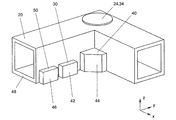
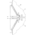
12 弾性エレメント
20、200 支持フレーム(ビーム)
21、22、23 セグメント
24 基準表面
25 センサ・ユニット
26 アクチュエータ
27 締付けデバイス
28 支持フレーム空胴
30、31、40、50 インターフェース表面
32 ロッド
34 インターフェース・ゾーン
42、44、46 ブロック
48 中空ビーム
51 インサート
52 接着剤
C 目標部分
F 力
IF 干渉計
IF1、IF2 位置センサ
IL 照明システム(イルミネータ)
M1、M2 マスク位置合せマーク
M1〜M6 光学アクティブ・ミラー
MA パターン化手段
MF 度量衡学フレーム
MT 第1の支持構造
P1、P2 基板位置合せマーク
PB 投影ビーム
PL 投影システム(投影光学系アセンブリ)
PM 第1の位置決め手段
PW 第2の位置決め手段
SO 放射源
VC 真空チャンバ
VP 真空ポンプ
W 基板
WT 基板テーブル
Claims (12)
- 投影放射ビームを提供するための照明システムと、
投影ビームの断面をパターン化するべく機能するパターン化手段を支持するための支持構造と、
基板を保持するための基板テーブルと、
パターン化されたビームを基板の目標部分に投射するための投影光学系アセンブリであって、前記アセンブリが、複数の可動光学エレメント及び対応する光学エレメントの位置及び/又は配向を感知するための複数のセンサ・ユニットを備え、前記可動光学エレメントが、支持フレーム上に間隔を隔てた関係で配置された投影光学系アセンブリとを備えたリソグラフィック装置であって、前記支持フレームが、相互接続された少なくとも2つのセグメントのアセンブリを備え、前記セグメントの各々が、前記複数の光学エレメントのうちの少なくとも1つを移動可能に取り付け、かつ、前記複数のセンサ・ユニットのうちの少なくとも1つを固定して取り付け、相互接続された前記少なくとも2つのセグメントが、内部に前記光学エレメントが前記間隔を隔てた関係で取り付けられる基準フレーム及び取付けフレームとして機能することを特徴とするリソグラフィック装置。 - 投影放射ビームを提供するための照明システムと、
投影ビームの断面をパターン化するべく機能するパターン化手段を支持するための支持構造と、
基板を保持するための基板テーブルと、
パターン化されたビームを基板の目標部分に投射するための投影光学系アセンブリであって、複数の可動光学エレメント及び対応する光学エレメントの位置及び/又は配向を感知するための複数のセンサ・ユニットを備え、前記可動光学エレメントが、支持フレーム上に間隔を隔てた関係で配置された投影光学系アセンブリとを備えたリソグラフィック装置であって、前記光学エレメントが、単一支持フレーム上に移動可能に取り付けられ、かつ、前記センサ・ユニットが、単一支持フレーム上に固定して取り付けられ、前記支持フレームが、内部に前記光学エレメントが前記間隔を隔てた関係で取り付けられる基準フレーム及び取付けフレームとして機能する1つのセグメントを備えることを特徴とするリソグラフィック装置。 - 前記1つ又は複数のセンサ・ユニットが、前記1つ又は複数のセグメント中若しくはセグメント上の所定の位置に直接取り付けられた、請求項1又は2に記載のリソグラフィック装置。
- 前記複数のセグメントが互いにスタック配列で相互接続するようになっている、請求項1、又は請求項1に従属したときの請求項3に記載のリソグラフィック装置。
- 前記支持フレームが3つのセグメントを備え、前記複数の光学エレメントのうちの2つが、前記セグメントのうちの少なくとも2つのセグメントの各々中に取り付けられた、請求項1、3又は4に記載のリソグラフィック装置。
- 前記センサ・ユニットが、前記1つ又は複数のセグメント上若しくはセグメント中に位置する基準表面に対する前記対応する光学エレメントの位置及び/又は配向を感知し、前記1つ又は複数のセグメントが、前記1つ又は複数のセグメント中に形成された、前記センサ・ユニットを受け入れるためのインターフェース表面を備え、前記インターフェース表面が、前記基準表面に対して予め決定された前記所定の位置に配置された、請求項3から5までのいずれかに記載のリソグラフィック装置。
- 前記支持フレームが複数のインサートを備え、前記インサートが、使用中にインターフェース・ゾーンを形成するべく、前記セグメント間に配置されるようになっており、したがって組立て状態では前記インサートが互いに接触し、前記接触しているインサートによって画定される表面の少なくとも一部が基準表面を形成する、請求項1又は3から6までのいずれかに記載のリソグラフィック装置。
- 前記1つ又は複数のセグメントが、前記複数の光学エレメントのうちの前記対応する1つに結合されたアクチュエータを固定して支持し、前記アクチュエータがセンサ・ユニットに応答して前記光学エレメントを所定の位置に移動させる、請求項1から7までのいずれかに記載のリソグラフィック装置。
- 組み立てられると、前記セグメントが実質的に水平面内で互いにインターフェースする、請求項1又は3から8までのいずれかに記載のリソグラフィック装置。
- 相互接続可能な複数のセグメントを提供するステップと、
個々のセグメントの上に、互いに間隔を隔てた関係で配置された複数の光学エレメントを移動可能に取り付け、かつ、前記移動可能に取り付けられた前記複数の前記光学エレメントのうちの1つの位置及び/又は配向を感知すべく、少なくとも1つのセンシング・エレメントを固定して取り付けるステップと、
内部に前記光学エレメントが前記間隔を隔てた関係で取り付けられる基準フレーム及び取付けフレームとして機能する単一セグメント化可能支持フレームの少なくとも一部を形成するべく、前記セグメントを相互接続するステップとを含む、リソグラフィック装置のための投影光学系アセンブリを組み立てる方法。 - 互いに間隔を隔てた関係で配置された複数の光学エレメントのための基準フレーム及び取付けフレームとして機能する1つのセグメント、及び前記複数の光学エレメントのうちの1つに関連して設けられた、移動可能光学エレメントの位置及び/又は配向を正確に測定するためのセンサ・ユニットを備えた単一支持フレームを提供するステップと、
前記複数の光学エレメントを前記フレーム上に移動可能に取り付け、かつ、前記センサ・ユニットを前記フレーム上に固定して取り付けるステップとを含む、リソグラフィック装置のための投影光学系アセンブリを組み立てる方法。 - 基板を提供するステップと、
照明システムを使用して投影放射ビームを提供するステップと、
前記投影ビームの断面をパターン化するべくパターン化手段を使用するステップと、
パターン化された放射ビームを、請求項1から9までのいずれかに記載されている投影光学系アセンブリを使用して前記基板の目標部分に投射するステップとを含むデバイス製造方法。
Applications Claiming Priority (2)
| Application Number | Priority Date | Filing Date | Title |
|---|---|---|---|
| EP03077785.8 | 2003-09-04 | ||
| EP03077785A EP1513018A1 (en) | 2003-09-04 | 2003-09-04 | Lithographic apparatus and device manufacturing method |
Related Parent Applications (1)
| Application Number | Title | Priority Date | Filing Date |
|---|---|---|---|
| JP2004257074A Division JP4408775B2 (ja) | 2003-09-04 | 2004-09-03 | リソグラフィック装置及びデバイス製造方法 |
Publications (2)
| Publication Number | Publication Date |
|---|---|
| JP2010004086A true JP2010004086A (ja) | 2010-01-07 |
| JP4903848B2 JP4903848B2 (ja) | 2012-03-28 |
Family
ID=34130245
Family Applications (2)
| Application Number | Title | Priority Date | Filing Date |
|---|---|---|---|
| JP2004257074A Expired - Fee Related JP4408775B2 (ja) | 2003-09-04 | 2004-09-03 | リソグラフィック装置及びデバイス製造方法 |
| JP2009233515A Expired - Fee Related JP4903848B2 (ja) | 2003-09-04 | 2009-10-07 | リソグラフィック装置及びデバイス製造方法 |
Family Applications Before (1)
| Application Number | Title | Priority Date | Filing Date |
|---|---|---|---|
| JP2004257074A Expired - Fee Related JP4408775B2 (ja) | 2003-09-04 | 2004-09-03 | リソグラフィック装置及びデバイス製造方法 |
Country Status (7)
| Country | Link |
|---|---|
| US (1) | US7161658B2 (ja) |
| EP (1) | EP1513018A1 (ja) |
| JP (2) | JP4408775B2 (ja) |
| KR (2) | KR20060021427A (ja) |
| CN (2) | CN100557511C (ja) |
| SG (1) | SG109613A1 (ja) |
| TW (1) | TWI245971B (ja) |
Cited By (1)
| Publication number | Priority date | Publication date | Assignee | Title |
|---|---|---|---|---|
| JP2017531206A (ja) * | 2014-09-15 | 2017-10-19 | カール・ツァイス・エスエムティー・ゲーエムベーハー | セラミックコンポーネント間の圧力嵌め接続用の接続機構 |
Families Citing this family (14)
| Publication number | Priority date | Publication date | Assignee | Title |
|---|---|---|---|---|
| EP1865381A4 (en) * | 2005-03-29 | 2010-03-03 | Nikon Corp | EXPOSURE DEVICE, METHOD FOR THE PRODUCTION OF AN EXPOSURE DEVICE AND METHOD FOR THE PRODUCTION OF A MICRO-BUILDING ELEMENT |
| JP4817702B2 (ja) * | 2005-04-14 | 2011-11-16 | キヤノン株式会社 | 光学装置及びそれを備えた露光装置 |
| US7936443B2 (en) * | 2006-05-09 | 2011-05-03 | Asml Netherlands B.V. | Lithographic apparatus and device manufacturing method |
| US8908144B2 (en) * | 2006-09-27 | 2014-12-09 | Asml Netherlands B.V. | Lithographic apparatus and device manufacturing method |
| DE102009034166A1 (de) | 2008-08-11 | 2010-02-18 | Carl Zeiss Smt Ag | Kontaminationsarme optische Anordnung |
| NL2005013A (en) * | 2009-07-31 | 2011-02-02 | Asml Netherlands Bv | Positioning system, lithographic apparatus and method. |
| DE102009045223A1 (de) * | 2009-09-30 | 2011-03-31 | Carl Zeiss Smt Gmbh | Optische Anordnung in einer Projektionsbelichtungsanlage für die EUV-Lithographie |
| WO2012166204A1 (en) * | 2011-06-02 | 2012-12-06 | Nikon Corporation | Fly's eye optical mirror with a plurality of optical elements rotationally aligned along two axes |
| WO2013178277A1 (en) * | 2012-05-31 | 2013-12-05 | Carl Zeiss Smt Gmbh | Optical imaging arrangement with multiple metrology support units |
| CN103676489B (zh) * | 2012-09-14 | 2015-09-30 | 上海微电子装备有限公司 | 一种反射式物镜结构及其制造方法 |
| WO2015043682A1 (en) * | 2013-09-30 | 2015-04-02 | Carl Zeiss Smt Gmbh | Optical imaging arrangement with simplified manufacture |
| DE102015201870A1 (de) * | 2015-02-03 | 2016-08-04 | Carl Zeiss Smt Gmbh | Anordnung zur Positionsmanipulation eines Elementes, insbesondere in einem optischen System |
| DE102015211286A1 (de) * | 2015-06-18 | 2016-12-22 | Carl Zeiss Smt Gmbh | Abbildungssystem und verfahren |
| NL2020269A (en) * | 2017-02-10 | 2018-08-22 | Asml Netherlands Bv | Lithographic apparatus and device manufacturing method |
Citations (6)
| Publication number | Priority date | Publication date | Assignee | Title |
|---|---|---|---|---|
| JPH11345760A (ja) * | 1998-05-29 | 1999-12-14 | Nikon Corp | 露光装置 |
| JP2000091209A (ja) * | 1998-09-14 | 2000-03-31 | Nikon Corp | 露光装置の製造方法、露光装置、及びデバイス製造方法 |
| JP2001351855A (ja) * | 1999-11-30 | 2001-12-21 | Asm Lithography Bv | リソグラフィ投影装置およびこれを使ったデバイスの製造方法 |
| JP2002131605A (ja) * | 2000-08-18 | 2002-05-09 | Nikon Corp | 保持装置、光学素子保持装置、鏡筒及び露光装置並びにマイクロデバイスの製造方法 |
| JP2003158070A (ja) * | 2001-07-14 | 2003-05-30 | Asml Netherlands Bv | リソグラフィ装置およびデバイス製造方法 |
| JP2003203860A (ja) * | 2001-12-21 | 2003-07-18 | Asml Netherlands Bv | リソグラフィ装置およびデバイス製造方法 |
Family Cites Families (5)
| Publication number | Priority date | Publication date | Assignee | Title |
|---|---|---|---|---|
| KR20010030903A (ko) * | 1997-11-12 | 2001-04-16 | 오노 시게오 | 투영노광장치 |
| JP2000286189A (ja) * | 1999-03-31 | 2000-10-13 | Nikon Corp | 露光装置および露光方法ならびにデバイス製造方法 |
| US6727981B2 (en) * | 1999-07-19 | 2004-04-27 | Nikon Corporation | Illuminating optical apparatus and making method thereof, exposure apparatus and making method thereof, and device manufacturing method |
| JP3387861B2 (ja) * | 1999-09-09 | 2003-03-17 | キヤノン株式会社 | 露光装置、およびデバイス製造方法 |
| US20040051984A1 (en) * | 2002-06-25 | 2004-03-18 | Nikon Corporation | Devices and methods for cooling optical elements in optical systems, including optical systems used in vacuum environments |
-
2003
- 2003-09-04 EP EP03077785A patent/EP1513018A1/en not_active Withdrawn
-
2004
- 2004-09-01 SG SG200405054A patent/SG109613A1/en unknown
- 2004-09-01 TW TW093126400A patent/TWI245971B/zh not_active IP Right Cessation
- 2004-09-02 US US10/932,318 patent/US7161658B2/en not_active Expired - Lifetime
- 2004-09-03 CN CNB200410068653XA patent/CN100557511C/zh not_active Expired - Lifetime
- 2004-09-03 CN CN200910165718A patent/CN101614968A/zh active Pending
- 2004-09-03 KR KR1020040070157A patent/KR20060021427A/ko not_active Ceased
- 2004-09-03 JP JP2004257074A patent/JP4408775B2/ja not_active Expired - Fee Related
-
2007
- 2007-05-18 KR KR1020070048870A patent/KR100822848B1/ko not_active Expired - Fee Related
-
2009
- 2009-10-07 JP JP2009233515A patent/JP4903848B2/ja not_active Expired - Fee Related
Patent Citations (7)
| Publication number | Priority date | Publication date | Assignee | Title |
|---|---|---|---|---|
| JPH11345760A (ja) * | 1998-05-29 | 1999-12-14 | Nikon Corp | 露光装置 |
| JP2000091209A (ja) * | 1998-09-14 | 2000-03-31 | Nikon Corp | 露光装置の製造方法、露光装置、及びデバイス製造方法 |
| JP2001351855A (ja) * | 1999-11-30 | 2001-12-21 | Asm Lithography Bv | リソグラフィ投影装置およびこれを使ったデバイスの製造方法 |
| JP2002131605A (ja) * | 2000-08-18 | 2002-05-09 | Nikon Corp | 保持装置、光学素子保持装置、鏡筒及び露光装置並びにマイクロデバイスの製造方法 |
| JP2003158070A (ja) * | 2001-07-14 | 2003-05-30 | Asml Netherlands Bv | リソグラフィ装置およびデバイス製造方法 |
| JP2003163160A (ja) * | 2001-07-14 | 2003-06-06 | Carl Zeiss Semiconductor Manufacturing Technologies Ag | 多数の光学要素を有する光学システム |
| JP2003203860A (ja) * | 2001-12-21 | 2003-07-18 | Asml Netherlands Bv | リソグラフィ装置およびデバイス製造方法 |
Cited By (2)
| Publication number | Priority date | Publication date | Assignee | Title |
|---|---|---|---|---|
| JP2017531206A (ja) * | 2014-09-15 | 2017-10-19 | カール・ツァイス・エスエムティー・ゲーエムベーハー | セラミックコンポーネント間の圧力嵌め接続用の接続機構 |
| US10571813B2 (en) | 2014-09-15 | 2020-02-25 | Carl Zeiss Smt Gmbh | Connection arrangement for a force-fit connection between ceramic components |
Also Published As
| Publication number | Publication date |
|---|---|
| JP2005086207A (ja) | 2005-03-31 |
| TW200513790A (en) | 2005-04-16 |
| CN101614968A (zh) | 2009-12-30 |
| TWI245971B (en) | 2005-12-21 |
| EP1513018A1 (en) | 2005-03-09 |
| KR100822848B1 (ko) | 2008-04-16 |
| KR20070059037A (ko) | 2007-06-11 |
| SG109613A1 (en) | 2005-03-30 |
| US7161658B2 (en) | 2007-01-09 |
| US20050083500A1 (en) | 2005-04-21 |
| CN100557511C (zh) | 2009-11-04 |
| JP4903848B2 (ja) | 2012-03-28 |
| KR20060021427A (ko) | 2006-03-08 |
| JP4408775B2 (ja) | 2010-02-03 |
| CN1591194A (zh) | 2005-03-09 |
Similar Documents
| Publication | Publication Date | Title |
|---|---|---|
| JP4903848B2 (ja) | リソグラフィック装置及びデバイス製造方法 | |
| JP4384181B2 (ja) | リソグラフィ装置およびデバイス製造方法 | |
| CN101276155B (zh) | 测量系统、光刻设备和测量方法 | |
| US6750949B2 (en) | Lithographic apparatus and device manufacturing method | |
| CN102929104B (zh) | 光学成像装置 | |
| CN104614950B (zh) | 光刻设备 | |
| US7061579B2 (en) | Lithographic apparatus and device manufacturing method | |
| US7049592B2 (en) | Lithographic apparatus and device manufacturing method | |
| EP1513022A1 (en) | Lithographic apparatus and device manufacturing method | |
| US7525637B2 (en) | Assembly |
Legal Events
| Date | Code | Title | Description |
|---|---|---|---|
| A521 | Request for written amendment filed |
Free format text: JAPANESE INTERMEDIATE CODE: A523 Effective date: 20091007 |
|
| A621 | Written request for application examination |
Free format text: JAPANESE INTERMEDIATE CODE: A621 Effective date: 20091007 |
|
| A131 | Notification of reasons for refusal |
Free format text: JAPANESE INTERMEDIATE CODE: A131 Effective date: 20110520 |
|
| A521 | Request for written amendment filed |
Free format text: JAPANESE INTERMEDIATE CODE: A523 Effective date: 20110804 |
|
| A131 | Notification of reasons for refusal |
Free format text: JAPANESE INTERMEDIATE CODE: A131 Effective date: 20110826 |
|
| A521 | Request for written amendment filed |
Free format text: JAPANESE INTERMEDIATE CODE: A523 Effective date: 20111028 |
|
| TRDD | Decision of grant or rejection written | ||
| A01 | Written decision to grant a patent or to grant a registration (utility model) |
Free format text: JAPANESE INTERMEDIATE CODE: A01 Effective date: 20111208 |
|
| A01 | Written decision to grant a patent or to grant a registration (utility model) |
Free format text: JAPANESE INTERMEDIATE CODE: A01 |
|
| A61 | First payment of annual fees (during grant procedure) |
Free format text: JAPANESE INTERMEDIATE CODE: A61 Effective date: 20120105 |
|
| R150 | Certificate of patent or registration of utility model |
Ref document number: 4903848 Country of ref document: JP Free format text: JAPANESE INTERMEDIATE CODE: R150 Free format text: JAPANESE INTERMEDIATE CODE: R150 |
|
| FPAY | Renewal fee payment (event date is renewal date of database) |
Free format text: PAYMENT UNTIL: 20150113 Year of fee payment: 3 |
|
| R250 | Receipt of annual fees |
Free format text: JAPANESE INTERMEDIATE CODE: R250 |
|
| R250 | Receipt of annual fees |
Free format text: JAPANESE INTERMEDIATE CODE: R250 |
|
| R250 | Receipt of annual fees |
Free format text: JAPANESE INTERMEDIATE CODE: R250 |
|
| R250 | Receipt of annual fees |
Free format text: JAPANESE INTERMEDIATE CODE: R250 |
|
| R250 | Receipt of annual fees |
Free format text: JAPANESE INTERMEDIATE CODE: R250 |
|
| R250 | Receipt of annual fees |
Free format text: JAPANESE INTERMEDIATE CODE: R250 |
|
| R250 | Receipt of annual fees |
Free format text: JAPANESE INTERMEDIATE CODE: R250 |
|
| LAPS | Cancellation because of no payment of annual fees |