JP2010004045A - 量子ドット構造を有する光学装置 - Google Patents
量子ドット構造を有する光学装置 Download PDFInfo
- Publication number
- JP2010004045A JP2010004045A JP2009146068A JP2009146068A JP2010004045A JP 2010004045 A JP2010004045 A JP 2010004045A JP 2009146068 A JP2009146068 A JP 2009146068A JP 2009146068 A JP2009146068 A JP 2009146068A JP 2010004045 A JP2010004045 A JP 2010004045A
- Authority
- JP
- Japan
- Prior art keywords
- quantum dot
- optical device
- spacer layer
- layer
- layers
- Prior art date
- Legal status (The legal status is an assumption and is not a legal conclusion. Google has not performed a legal analysis and makes no representation as to the accuracy of the status listed.)
- Granted
Links
Images

Classifications
-
- H—ELECTRICITY
- H10—SEMICONDUCTOR DEVICES; ELECTRIC SOLID-STATE DEVICES NOT OTHERWISE PROVIDED FOR
- H10D—INORGANIC ELECTRIC SEMICONDUCTOR DEVICES
- H10D62/00—Semiconductor bodies, or regions thereof, of devices having potential barriers
- H10D62/80—Semiconductor bodies, or regions thereof, of devices having potential barriers characterised by the materials
- H10D62/81—Semiconductor bodies, or regions thereof, of devices having potential barriers characterised by the materials of structures exhibiting quantum-confinement effects, e.g. single quantum wells; of structures having periodic or quasi-periodic potential variation
- H10D62/812—Single quantum well structures
- H10D62/814—Quantum box structures
-
- B—PERFORMING OPERATIONS; TRANSPORTING
- B82—NANOTECHNOLOGY
- B82Y—SPECIFIC USES OR APPLICATIONS OF NANOSTRUCTURES; MEASUREMENT OR ANALYSIS OF NANOSTRUCTURES; MANUFACTURE OR TREATMENT OF NANOSTRUCTURES
- B82Y10/00—Nanotechnology for information processing, storage or transmission, e.g. quantum computing or single electron logic
-
- B—PERFORMING OPERATIONS; TRANSPORTING
- B82—NANOTECHNOLOGY
- B82Y—SPECIFIC USES OR APPLICATIONS OF NANOSTRUCTURES; MEASUREMENT OR ANALYSIS OF NANOSTRUCTURES; MANUFACTURE OR TREATMENT OF NANOSTRUCTURES
- B82Y20/00—Nanooptics, e.g. quantum optics or photonic crystals
-
- H—ELECTRICITY
- H01—ELECTRIC ELEMENTS
- H01S—DEVICES USING THE PROCESS OF LIGHT AMPLIFICATION BY STIMULATED EMISSION OF RADIATION [LASER] TO AMPLIFY OR GENERATE LIGHT; DEVICES USING STIMULATED EMISSION OF ELECTROMAGNETIC RADIATION IN WAVE RANGES OTHER THAN OPTICAL
- H01S5/00—Semiconductor lasers
- H01S5/30—Structure or shape of the active region; Materials used for the active region
- H01S5/34—Structure or shape of the active region; Materials used for the active region comprising quantum well or superlattice structures, e.g. single quantum well [SQW] lasers, multiple quantum well [MQW] lasers or graded index separate confinement heterostructure [GRINSCH] lasers
- H01S5/3403—Structure or shape of the active region; Materials used for the active region comprising quantum well or superlattice structures, e.g. single quantum well [SQW] lasers, multiple quantum well [MQW] lasers or graded index separate confinement heterostructure [GRINSCH] lasers having a strained layer structure in which the strain performs a special function, e.g. general strain effects, strain versus polarisation
- H01S5/3406—Structure or shape of the active region; Materials used for the active region comprising quantum well or superlattice structures, e.g. single quantum well [SQW] lasers, multiple quantum well [MQW] lasers or graded index separate confinement heterostructure [GRINSCH] lasers having a strained layer structure in which the strain performs a special function, e.g. general strain effects, strain versus polarisation including strain compensation
-
- H—ELECTRICITY
- H01—ELECTRIC ELEMENTS
- H01S—DEVICES USING THE PROCESS OF LIGHT AMPLIFICATION BY STIMULATED EMISSION OF RADIATION [LASER] TO AMPLIFY OR GENERATE LIGHT; DEVICES USING STIMULATED EMISSION OF ELECTROMAGNETIC RADIATION IN WAVE RANGES OTHER THAN OPTICAL
- H01S5/00—Semiconductor lasers
- H01S5/30—Structure or shape of the active region; Materials used for the active region
- H01S5/34—Structure or shape of the active region; Materials used for the active region comprising quantum well or superlattice structures, e.g. single quantum well [SQW] lasers, multiple quantum well [MQW] lasers or graded index separate confinement heterostructure [GRINSCH] lasers
- H01S5/341—Structures having reduced dimensionality, e.g. quantum wires
- H01S5/3412—Structures having reduced dimensionality, e.g. quantum wires quantum box or quantum dash
-
- H—ELECTRICITY
- H01—ELECTRIC ELEMENTS
- H01S—DEVICES USING THE PROCESS OF LIGHT AMPLIFICATION BY STIMULATED EMISSION OF RADIATION [LASER] TO AMPLIFY OR GENERATE LIGHT; DEVICES USING STIMULATED EMISSION OF ELECTROMAGNETIC RADIATION IN WAVE RANGES OTHER THAN OPTICAL
- H01S5/00—Semiconductor lasers
- H01S5/30—Structure or shape of the active region; Materials used for the active region
- H01S5/34—Structure or shape of the active region; Materials used for the active region comprising quantum well or superlattice structures, e.g. single quantum well [SQW] lasers, multiple quantum well [MQW] lasers or graded index separate confinement heterostructure [GRINSCH] lasers
- H01S5/343—Structure or shape of the active region; Materials used for the active region comprising quantum well or superlattice structures, e.g. single quantum well [SQW] lasers, multiple quantum well [MQW] lasers or graded index separate confinement heterostructure [GRINSCH] lasers in AIIIBV compounds, e.g. AlGaAs-laser, InP-based laser
- H01S5/34346—Structure or shape of the active region; Materials used for the active region comprising quantum well or superlattice structures, e.g. single quantum well [SQW] lasers, multiple quantum well [MQW] lasers or graded index separate confinement heterostructure [GRINSCH] lasers in AIIIBV compounds, e.g. AlGaAs-laser, InP-based laser characterised by the materials of the barrier layers
- H01S5/34373—Structure or shape of the active region; Materials used for the active region comprising quantum well or superlattice structures, e.g. single quantum well [SQW] lasers, multiple quantum well [MQW] lasers or graded index separate confinement heterostructure [GRINSCH] lasers in AIIIBV compounds, e.g. AlGaAs-laser, InP-based laser characterised by the materials of the barrier layers based on InGa(Al)AsP
-
- Y—GENERAL TAGGING OF NEW TECHNOLOGICAL DEVELOPMENTS; GENERAL TAGGING OF CROSS-SECTIONAL TECHNOLOGIES SPANNING OVER SEVERAL SECTIONS OF THE IPC; TECHNICAL SUBJECTS COVERED BY FORMER USPC CROSS-REFERENCE ART COLLECTIONS [XRACs] AND DIGESTS
- Y10—TECHNICAL SUBJECTS COVERED BY FORMER USPC
- Y10S—TECHNICAL SUBJECTS COVERED BY FORMER USPC CROSS-REFERENCE ART COLLECTIONS [XRACs] AND DIGESTS
- Y10S438/00—Semiconductor device manufacturing: process
- Y10S438/962—Quantum dots and lines
Landscapes
- Engineering & Computer Science (AREA)
- Chemical & Material Sciences (AREA)
- Nanotechnology (AREA)
- Physics & Mathematics (AREA)
- Crystallography & Structural Chemistry (AREA)
- Life Sciences & Earth Sciences (AREA)
- Biophysics (AREA)
- Optics & Photonics (AREA)
- Mathematical Physics (AREA)
- Theoretical Computer Science (AREA)
- Semiconductor Lasers (AREA)
Abstract
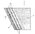
【解決手段】スペーサ層(15)はバリア層(12)上で成長させられ、それによってスペーサ層(15)は、量子ドット層によって生じる歪場を実質的に遮断するようになっており、したがって、次のバリア層(12)に対する円滑な成長最前部が作り出される。
【選択図】図2
Description
Claims (18)
- 1つまたは複数の量子ドット層(13)および1つまたは複数のバリア層(12)を有する光学装置を製造する方法であって、バリア層(12)上で、前記バリア層によって生じる歪場を実質的に遮断するようになっているスペーサ層(15)を成長させるステップを含む方法。
- 前記スペーサ層(15)は、成長最前部がほぼ円滑な表面(17a)を有した状態で成長させられる、請求項1に記載の方法。
- 次のバリア層(12)は、前記スペーサ層(15)上で成長させられ、円滑な表面(17b)を備えた成長最前部を有する、請求項1または請求項2に記載の方法。
- InP材料のスペーサ層は、次の量子ドット層の間に置かれ、使用の際、トンネル効果による量子ドット層間の結合を可能にする、請求項1乃至3のいずれか1項に記載の方法。
- 1つまたは複数の量子ドット層(13)および1つまたは複数のバリア層(12)を有する光学装置であって、さらにバリア層(12)上にスペーサ層(15)を備え、前記スペーサ層(15)は、バリア層(12)によって生じる歪場を実質的に遮断するようになっている光学装置。
- 2つ以上の量子ドット層および3つ以上のバリア層を有することができる、請求項5に記載の光学装置。
- 前記スペーサ層(15)は、ほぼ円滑な表面を有する、請求項5または請求項6に記載の光学装置。
- 次のバリア層(12)は前記スペーサ層(15)上で成長させられ、ほぼ円滑な表面(17b)を有する、請求項5乃至7のいずれか1項に記載の光学装置。
- 前記スペーサ層(15)は、2成分材料で作られている、請求項5乃至8のいずれか1項に記載の光学装置。
- 前記2成分材料はInPである、請求項9に記載の光学装置。
- 前記スペーサ層(15)は、約3nmの厚さを有する、請求項5乃至10のいずれか1項に記載の光学装置。
- 次の2つの量子ドット層間の分離は、約5nmである、請求項5乃至11のいずれか1項に記載の光学装置。
- InP材料のスペーサ層は、トンネル効果による量子ドット層間の結合を可能にするようになっている次の量子ドット層間に置かれている、請求項5乃至12のいずれか1項に記載の光学装置。
- 請求項5乃至13のいずれか1項に記載の光学装置を備えた、光信号処理を行うユニット。
- クロック修復ユニットである、請求項14に記載のユニット。
- 光増幅ユニットである、請求項14に記載のユニット。
- 波長変換ユニットである、請求項14に記載のユニット。
- 信号処理ユニットである、請求項14に記載のユニット。
Applications Claiming Priority (2)
| Application Number | Priority Date | Filing Date | Title |
|---|---|---|---|
| EP08305281.1A EP2136445B1 (en) | 2008-06-19 | 2008-06-19 | An optical device having a quantum-dot structure |
| EP08305281.1 | 2008-06-19 |
Publications (2)
| Publication Number | Publication Date |
|---|---|
| JP2010004045A true JP2010004045A (ja) | 2010-01-07 |
| JP5384217B2 JP5384217B2 (ja) | 2014-01-08 |
Family
ID=40011281
Family Applications (1)
| Application Number | Title | Priority Date | Filing Date |
|---|---|---|---|
| JP2009146068A Expired - Fee Related JP5384217B2 (ja) | 2008-06-19 | 2009-06-19 | 量子ドット構造を有する光学装置 |
Country Status (5)
| Country | Link |
|---|---|
| US (1) | US7968863B2 (ja) |
| EP (1) | EP2136445B1 (ja) |
| JP (1) | JP5384217B2 (ja) |
| KR (1) | KR20090132529A (ja) |
| CN (1) | CN101609960B (ja) |
Families Citing this family (5)
| Publication number | Priority date | Publication date | Assignee | Title |
|---|---|---|---|---|
| EP2136445B1 (en) * | 2008-06-19 | 2016-04-13 | Alcatel Lucent | An optical device having a quantum-dot structure |
| FR2967905B1 (fr) * | 2010-11-25 | 2013-07-12 | Oreal | Procede de traitement de la transpiration utilisant un compose carbonyle susceptible de reagir selon la reaction de maillard |
| KR102353095B1 (ko) * | 2014-12-26 | 2022-01-19 | 엔에스 마테리얼스 아이엔씨. | 파장 변환 부재 및 그 제조 방법 |
| US10236659B2 (en) | 2017-04-04 | 2019-03-19 | Rochester Institute Of Technology | Mode-locked lasers on silicon by palladium bonding and methods therefor |
| CN108983446B (zh) * | 2017-06-01 | 2021-04-06 | Tcl科技集团股份有限公司 | 一种光强调制器 |
Citations (3)
| Publication number | Priority date | Publication date | Assignee | Title |
|---|---|---|---|---|
| WO2004055900A1 (ja) * | 2002-12-16 | 2004-07-01 | Japan Science And Technology Agency | 不均一な量子ドットを有する半導体積層構造、それを用いた発光ダイオード、半導体レーザダイオード及び半導体光増幅器並びにそれらの製造方法 |
| JP2005072338A (ja) * | 2003-08-26 | 2005-03-17 | Fujitsu Ltd | 光半導体装置及びその製造方法 |
| JP2007157975A (ja) * | 2005-12-05 | 2007-06-21 | Fujitsu Ltd | 半導体装置の製造方法 |
Family Cites Families (4)
| Publication number | Priority date | Publication date | Assignee | Title |
|---|---|---|---|---|
| JP3468866B2 (ja) | 1994-09-16 | 2003-11-17 | 富士通株式会社 | 3次元量子閉じ込めを利用した半導体装置 |
| JP3672678B2 (ja) | 1996-04-05 | 2005-07-20 | 富士通株式会社 | 量子半導体装置およびその製造方法 |
| JP4952005B2 (ja) * | 2006-03-07 | 2012-06-13 | 富士通株式会社 | 半導体素子およびその製造方法 |
| EP2136445B1 (en) * | 2008-06-19 | 2016-04-13 | Alcatel Lucent | An optical device having a quantum-dot structure |
-
2008
- 2008-06-19 EP EP08305281.1A patent/EP2136445B1/en not_active Not-in-force
-
2009
- 2009-06-11 US US12/457,463 patent/US7968863B2/en not_active Expired - Fee Related
- 2009-06-18 CN CN200910147531.2A patent/CN101609960B/zh not_active Expired - Fee Related
- 2009-06-18 KR KR1020090054356A patent/KR20090132529A/ko not_active Ceased
- 2009-06-19 JP JP2009146068A patent/JP5384217B2/ja not_active Expired - Fee Related
Patent Citations (3)
| Publication number | Priority date | Publication date | Assignee | Title |
|---|---|---|---|---|
| WO2004055900A1 (ja) * | 2002-12-16 | 2004-07-01 | Japan Science And Technology Agency | 不均一な量子ドットを有する半導体積層構造、それを用いた発光ダイオード、半導体レーザダイオード及び半導体光増幅器並びにそれらの製造方法 |
| JP2005072338A (ja) * | 2003-08-26 | 2005-03-17 | Fujitsu Ltd | 光半導体装置及びその製造方法 |
| JP2007157975A (ja) * | 2005-12-05 | 2007-06-21 | Fujitsu Ltd | 半導体装置の製造方法 |
Also Published As
| Publication number | Publication date |
|---|---|
| US7968863B2 (en) | 2011-06-28 |
| JP5384217B2 (ja) | 2014-01-08 |
| CN101609960A (zh) | 2009-12-23 |
| KR20090132529A (ko) | 2009-12-30 |
| EP2136445A1 (en) | 2009-12-23 |
| CN101609960B (zh) | 2014-10-15 |
| EP2136445B1 (en) | 2016-04-13 |
| US20090315019A1 (en) | 2009-12-24 |
Similar Documents
| Publication | Publication Date | Title |
|---|---|---|
| Lu et al. | CW lasing of current injection blue GaN-based vertical cavity surface emitting laser | |
| JP3854560B2 (ja) | 量子光半導体装置 | |
| JP6300240B2 (ja) | 半導体デバイス | |
| Sugawara et al. | Quantum dot devices: Handling the heat. | |
| Lodahl et al. | A deterministic source of single photons | |
| JP5384217B2 (ja) | 量子ドット構造を有する光学装置 | |
| EP0647001B1 (en) | Polarization insensitive semiconductor optical amplifier | |
| CN103119810B (zh) | 半导体装置 | |
| JP5374894B2 (ja) | 半導体光増幅器及びその製造方法並びに半導体光集積素子 | |
| WO2013118248A1 (ja) | 発光素子 | |
| WO2017210300A1 (en) | Integration of direct-bandgap optically active devices on indirect-bandgap-based substrates | |
| US5263040A (en) | Strained quantum well laser diode | |
| JP4983790B2 (ja) | 光半導体装置とその製造方法 | |
| JP2004087749A (ja) | 量子ドットを有する半導体光装置 | |
| JP2008216883A (ja) | フォトニック結晶共振器、光子対発生装置、光子位相変調装置 | |
| CN105048285A (zh) | 一种提高氮化镓基激光器性能的方法 | |
| JP3816924B2 (ja) | 半導体導波型光制御素子 | |
| JP6437869B2 (ja) | 半導体レーザ | |
| Brenot et al. | Quantum dots semiconductor optical amplifier with a-3dB bandwidth of up to 120 nm in semi-cooled operation | |
| JP3230576B2 (ja) | 半導体発光素子 | |
| JP2008091420A (ja) | 量子ドット光半導体素子の製造方法 | |
| JPH1090738A (ja) | 非線形光デバイス | |
| Sugawara et al. | Handling the heat | |
| JP4972995B2 (ja) | 量子ドット半導体装置 | |
| JP5641099B2 (ja) | 半導体光増幅器及びその製造方法並びに半導体光集積素子 |
Legal Events
| Date | Code | Title | Description |
|---|---|---|---|
| A977 | Report on retrieval |
Free format text: JAPANESE INTERMEDIATE CODE: A971007 Effective date: 20120227 |
|
| A131 | Notification of reasons for refusal |
Free format text: JAPANESE INTERMEDIATE CODE: A131 Effective date: 20120319 |
|
| A601 | Written request for extension of time |
Free format text: JAPANESE INTERMEDIATE CODE: A601 Effective date: 20120619 |
|
| A602 | Written permission of extension of time |
Free format text: JAPANESE INTERMEDIATE CODE: A602 Effective date: 20120622 |
|
| RD04 | Notification of resignation of power of attorney |
Free format text: JAPANESE INTERMEDIATE CODE: A7424 Effective date: 20120710 |
|
| A521 | Request for written amendment filed |
Free format text: JAPANESE INTERMEDIATE CODE: A523 Effective date: 20120919 |
|
| A02 | Decision of refusal |
Free format text: JAPANESE INTERMEDIATE CODE: A02 Effective date: 20130402 |
|
| A521 | Request for written amendment filed |
Free format text: JAPANESE INTERMEDIATE CODE: A523 Effective date: 20130802 |
|
| A911 | Transfer to examiner for re-examination before appeal (zenchi) |
Free format text: JAPANESE INTERMEDIATE CODE: A911 Effective date: 20130809 |
|
| TRDD | Decision of grant or rejection written | ||
| A01 | Written decision to grant a patent or to grant a registration (utility model) |
Free format text: JAPANESE INTERMEDIATE CODE: A01 Effective date: 20130903 |
|
| A61 | First payment of annual fees (during grant procedure) |
Free format text: JAPANESE INTERMEDIATE CODE: A61 Effective date: 20131002 |
|
| R150 | Certificate of patent or registration of utility model |
Free format text: JAPANESE INTERMEDIATE CODE: R150 Ref document number: 5384217 Country of ref document: JP Free format text: JAPANESE INTERMEDIATE CODE: R150 |
|
| R250 | Receipt of annual fees |
Free format text: JAPANESE INTERMEDIATE CODE: R250 |
|
| R250 | Receipt of annual fees |
Free format text: JAPANESE INTERMEDIATE CODE: R250 |
|
| R250 | Receipt of annual fees |
Free format text: JAPANESE INTERMEDIATE CODE: R250 |
|
| S111 | Request for change of ownership or part of ownership |
Free format text: JAPANESE INTERMEDIATE CODE: R313113 |
|
| S531 | Written request for registration of change of domicile |
Free format text: JAPANESE INTERMEDIATE CODE: R313531 |
|
| R371 | Transfer withdrawn |
Free format text: JAPANESE INTERMEDIATE CODE: R371 |
|
| S111 | Request for change of ownership or part of ownership |
Free format text: JAPANESE INTERMEDIATE CODE: R313113 |
|
| S531 | Written request for registration of change of domicile |
Free format text: JAPANESE INTERMEDIATE CODE: R313531 |
|
| R350 | Written notification of registration of transfer |
Free format text: JAPANESE INTERMEDIATE CODE: R350 |
|
| R250 | Receipt of annual fees |
Free format text: JAPANESE INTERMEDIATE CODE: R250 |
|
| R250 | Receipt of annual fees |
Free format text: JAPANESE INTERMEDIATE CODE: R250 |
|
| LAPS | Cancellation because of no payment of annual fees |