JP2010004045A - Optical device having quantum-dot structure - Google Patents
Optical device having quantum-dot structure Download PDFInfo
- Publication number
- JP2010004045A JP2010004045A JP2009146068A JP2009146068A JP2010004045A JP 2010004045 A JP2010004045 A JP 2010004045A JP 2009146068 A JP2009146068 A JP 2009146068A JP 2009146068 A JP2009146068 A JP 2009146068A JP 2010004045 A JP2010004045 A JP 2010004045A
- Authority
- JP
- Japan
- Prior art keywords
- quantum dot
- optical device
- spacer layer
- layer
- layers
- Prior art date
- Legal status (The legal status is an assumption and is not a legal conclusion. Google has not performed a legal analysis and makes no representation as to the accuracy of the status listed.)
- Granted
Links
- 239000002096 quantum dot Substances 0.000 title claims abstract description 64
- 230000003287 optical effect Effects 0.000 title claims abstract description 49
- 125000006850 spacer group Chemical group 0.000 claims abstract description 42
- 230000004888 barrier function Effects 0.000 claims abstract description 37
- 238000004519 manufacturing process Methods 0.000 claims abstract description 4
- 239000000463 material Substances 0.000 claims description 21
- 230000008878 coupling Effects 0.000 claims description 7
- 238000010168 coupling process Methods 0.000 claims description 7
- 238000005859 coupling reaction Methods 0.000 claims description 7
- 238000000034 method Methods 0.000 claims description 7
- 230000000694 effects Effects 0.000 claims description 6
- 238000012545 processing Methods 0.000 claims description 5
- 238000000926 separation method Methods 0.000 claims description 4
- 230000003321 amplification Effects 0.000 claims description 3
- 238000003199 nucleic acid amplification method Methods 0.000 claims description 3
- 230000005641 tunneling Effects 0.000 claims description 3
- 238000006243 chemical reaction Methods 0.000 claims description 2
- 230000010287 polarization Effects 0.000 description 14
- 230000035945 sensitivity Effects 0.000 description 10
- 230000008901 benefit Effects 0.000 description 8
- 230000008021 deposition Effects 0.000 description 3
- 238000002474 experimental method Methods 0.000 description 3
- 239000013307 optical fiber Substances 0.000 description 3
- 239000004065 semiconductor Substances 0.000 description 3
- 239000000758 substrate Substances 0.000 description 3
- 230000005540 biological transmission Effects 0.000 description 2
- 230000000593 degrading effect Effects 0.000 description 2
- 238000005137 deposition process Methods 0.000 description 2
- RPQDHPTXJYYUPQ-UHFFFAOYSA-N indium arsenide Chemical compound [In]#[As] RPQDHPTXJYYUPQ-UHFFFAOYSA-N 0.000 description 2
- 230000008569 process Effects 0.000 description 2
- 229910001218 Gallium arsenide Inorganic materials 0.000 description 1
- 229910000673 Indium arsenide Inorganic materials 0.000 description 1
- 239000011149 active material Substances 0.000 description 1
- 239000000969 carrier Substances 0.000 description 1
- 230000008859 change Effects 0.000 description 1
- 238000007796 conventional method Methods 0.000 description 1
- 230000007547 defect Effects 0.000 description 1
- 230000001066 destructive effect Effects 0.000 description 1
- 230000001627 detrimental effect Effects 0.000 description 1
- 239000000835 fiber Substances 0.000 description 1
- 238000009499 grossing Methods 0.000 description 1
- 238000001000 micrograph Methods 0.000 description 1
- 230000005693 optoelectronics Effects 0.000 description 1
- 238000004806 packaging method and process Methods 0.000 description 1
- 230000006798 recombination Effects 0.000 description 1
- 238000005215 recombination Methods 0.000 description 1
- 238000011084 recovery Methods 0.000 description 1
- 230000007480 spreading Effects 0.000 description 1
Images

Classifications
-
- H—ELECTRICITY
- H01—ELECTRIC ELEMENTS
- H01L—SEMICONDUCTOR DEVICES NOT COVERED BY CLASS H10
- H01L29/00—Semiconductor devices adapted for rectifying, amplifying, oscillating or switching, or capacitors or resistors with at least one potential-jump barrier or surface barrier, e.g. PN junction depletion layer or carrier concentration layer; Details of semiconductor bodies or of electrodes thereof ; Multistep manufacturing processes therefor
- H01L29/02—Semiconductor bodies ; Multistep manufacturing processes therefor
- H01L29/12—Semiconductor bodies ; Multistep manufacturing processes therefor characterised by the materials of which they are formed
- H01L29/122—Single quantum well structures
- H01L29/127—Quantum box structures
-
- B—PERFORMING OPERATIONS; TRANSPORTING
- B82—NANOTECHNOLOGY
- B82Y—SPECIFIC USES OR APPLICATIONS OF NANOSTRUCTURES; MEASUREMENT OR ANALYSIS OF NANOSTRUCTURES; MANUFACTURE OR TREATMENT OF NANOSTRUCTURES
- B82Y10/00—Nanotechnology for information processing, storage or transmission, e.g. quantum computing or single electron logic
-
- B—PERFORMING OPERATIONS; TRANSPORTING
- B82—NANOTECHNOLOGY
- B82Y—SPECIFIC USES OR APPLICATIONS OF NANOSTRUCTURES; MEASUREMENT OR ANALYSIS OF NANOSTRUCTURES; MANUFACTURE OR TREATMENT OF NANOSTRUCTURES
- B82Y20/00—Nanooptics, e.g. quantum optics or photonic crystals
-
- H—ELECTRICITY
- H01—ELECTRIC ELEMENTS
- H01S—DEVICES USING THE PROCESS OF LIGHT AMPLIFICATION BY STIMULATED EMISSION OF RADIATION [LASER] TO AMPLIFY OR GENERATE LIGHT; DEVICES USING STIMULATED EMISSION OF ELECTROMAGNETIC RADIATION IN WAVE RANGES OTHER THAN OPTICAL
- H01S5/00—Semiconductor lasers
- H01S5/30—Structure or shape of the active region; Materials used for the active region
- H01S5/34—Structure or shape of the active region; Materials used for the active region comprising quantum well or superlattice structures, e.g. single quantum well [SQW] lasers, multiple quantum well [MQW] lasers or graded index separate confinement heterostructure [GRINSCH] lasers
- H01S5/3403—Structure or shape of the active region; Materials used for the active region comprising quantum well or superlattice structures, e.g. single quantum well [SQW] lasers, multiple quantum well [MQW] lasers or graded index separate confinement heterostructure [GRINSCH] lasers having a strained layer structure in which the strain performs a special function, e.g. general strain effects, strain versus polarisation
- H01S5/3406—Structure or shape of the active region; Materials used for the active region comprising quantum well or superlattice structures, e.g. single quantum well [SQW] lasers, multiple quantum well [MQW] lasers or graded index separate confinement heterostructure [GRINSCH] lasers having a strained layer structure in which the strain performs a special function, e.g. general strain effects, strain versus polarisation including strain compensation
-
- H—ELECTRICITY
- H01—ELECTRIC ELEMENTS
- H01S—DEVICES USING THE PROCESS OF LIGHT AMPLIFICATION BY STIMULATED EMISSION OF RADIATION [LASER] TO AMPLIFY OR GENERATE LIGHT; DEVICES USING STIMULATED EMISSION OF ELECTROMAGNETIC RADIATION IN WAVE RANGES OTHER THAN OPTICAL
- H01S5/00—Semiconductor lasers
- H01S5/30—Structure or shape of the active region; Materials used for the active region
- H01S5/34—Structure or shape of the active region; Materials used for the active region comprising quantum well or superlattice structures, e.g. single quantum well [SQW] lasers, multiple quantum well [MQW] lasers or graded index separate confinement heterostructure [GRINSCH] lasers
- H01S5/341—Structures having reduced dimensionality, e.g. quantum wires
- H01S5/3412—Structures having reduced dimensionality, e.g. quantum wires quantum box or quantum dash
-
- H—ELECTRICITY
- H01—ELECTRIC ELEMENTS
- H01S—DEVICES USING THE PROCESS OF LIGHT AMPLIFICATION BY STIMULATED EMISSION OF RADIATION [LASER] TO AMPLIFY OR GENERATE LIGHT; DEVICES USING STIMULATED EMISSION OF ELECTROMAGNETIC RADIATION IN WAVE RANGES OTHER THAN OPTICAL
- H01S5/00—Semiconductor lasers
- H01S5/30—Structure or shape of the active region; Materials used for the active region
- H01S5/34—Structure or shape of the active region; Materials used for the active region comprising quantum well or superlattice structures, e.g. single quantum well [SQW] lasers, multiple quantum well [MQW] lasers or graded index separate confinement heterostructure [GRINSCH] lasers
- H01S5/343—Structure or shape of the active region; Materials used for the active region comprising quantum well or superlattice structures, e.g. single quantum well [SQW] lasers, multiple quantum well [MQW] lasers or graded index separate confinement heterostructure [GRINSCH] lasers in AIIIBV compounds, e.g. AlGaAs-laser, InP-based laser
- H01S5/34346—Structure or shape of the active region; Materials used for the active region comprising quantum well or superlattice structures, e.g. single quantum well [SQW] lasers, multiple quantum well [MQW] lasers or graded index separate confinement heterostructure [GRINSCH] lasers in AIIIBV compounds, e.g. AlGaAs-laser, InP-based laser characterised by the materials of the barrier layers
- H01S5/34373—Structure or shape of the active region; Materials used for the active region comprising quantum well or superlattice structures, e.g. single quantum well [SQW] lasers, multiple quantum well [MQW] lasers or graded index separate confinement heterostructure [GRINSCH] lasers in AIIIBV compounds, e.g. AlGaAs-laser, InP-based laser characterised by the materials of the barrier layers based on InGa(Al)AsP
-
- Y—GENERAL TAGGING OF NEW TECHNOLOGICAL DEVELOPMENTS; GENERAL TAGGING OF CROSS-SECTIONAL TECHNOLOGIES SPANNING OVER SEVERAL SECTIONS OF THE IPC; TECHNICAL SUBJECTS COVERED BY FORMER USPC CROSS-REFERENCE ART COLLECTIONS [XRACs] AND DIGESTS
- Y10—TECHNICAL SUBJECTS COVERED BY FORMER USPC
- Y10S—TECHNICAL SUBJECTS COVERED BY FORMER USPC CROSS-REFERENCE ART COLLECTIONS [XRACs] AND DIGESTS
- Y10S438/00—Semiconductor device manufacturing: process
- Y10S438/962—Quantum dots and lines
Abstract
Description
本発明は、オプトエレクトロニクスの分野に関する。より詳細には、本発明は、量子ドット構造を有する光学装置、およびこのような光学装置を備えた光信号処理ユニットに関する。 The present invention relates to the field of optoelectronics. More specifically, the present invention relates to an optical device having a quantum dot structure and an optical signal processing unit including such an optical device.
改善された性能を備えた光学装置を得るために、InAs/InGaAsPなどの構造を使用する量子ドット・ベース装置が、ますます魅力的となってきている。典型的には、基板はInPで作られており、活性材料はInGaAsPバリア内に埋め込まれたInAs量子ドットである。このような装置の例は、レーザ源、光増幅器、光学センサ(検出器)などである。量子ドット・ベース装置を使用する利点は主に、低チャープ、低ノイズ、低感温性、および広い波長応用例を与えることが可能であることにある。 In order to obtain optical devices with improved performance, quantum dot based devices using structures such as InAs / InGaAsP have become increasingly attractive. Typically, the substrate is made of InP and the active material is InAs quantum dots embedded in an InGaAsP barrier. Examples of such devices are laser sources, optical amplifiers, optical sensors (detectors) and the like. The advantage of using a quantum dot based device is mainly that it can provide low chirp, low noise, low temperature sensitivity, and wide wavelength applications.
量子井戸および量子ドット半導体構造は、関連する技術分野でよく知られている。手短に言うと、量子井戸構造は、2次元空間での電子またはホールの伝播を可能にしつつ、第3の次元でのこのような伝播を制限するように構成されており、量子ドット構造は、3次元でキャリヤを閉じ込めるように配置されている。 Quantum well and quantum dot semiconductor structures are well known in the relevant art. In short, the quantum well structure is configured to limit such propagation in the third dimension while allowing the propagation of electrons or holes in two-dimensional space, Arranged to confine the carrier in three dimensions.
光学装置に対して量子ドット構造を使用する1つの利点は、このような構造では、動的にモードロックされたレーザ内の比較的低いタイミング・ジッタを得ることができるということである。 One advantage of using quantum dot structures for optical devices is that such structures can achieve relatively low timing jitter in dynamically mode-locked lasers.
しかし、量子ドット・ベース装置は、偏光に関して比較的感度が高いという問題がある。これは、以下の理由により欠点である。知られているように、光源から伝達される光信号を偏光することができる。これは、光信号の成分の振動の方向が、光信号自体の伝播の方向と垂直であるということを意味する。偏光のよく知られている例は、それぞれTEモードおよびTMモードとして知られる、電気成分および磁気成分を有するものである。伝達された光信号は普通、光ファイバを通して光受信機に向かって前進する。実際、偏光した光信号が光ファイバに沿って前進する場合、その偏光状態に関する特定の歪みを受ける。これは、光ファイバは普通、光源から伝達されたときに偏光モードを元の状態に維持することが可能ではないからである。その結果、光信号は、歪んだ偏光のある受信機端部で受信される。したがって、受信機が偏光高感度装置である場合、受信した光信号を正確に処理することができない。既に上で述べたように、量子ドット・ベース装置は偏光感度が高く、したがってこのような欠点の問題がある。 However, quantum dot based devices have the problem of relatively high sensitivity with respect to polarization. This is a drawback for the following reasons. As is known, the optical signal transmitted from the light source can be polarized. This means that the direction of vibration of the component of the optical signal is perpendicular to the direction of propagation of the optical signal itself. Well-known examples of polarization are those having electrical and magnetic components, known as TE mode and TM mode, respectively. The transmitted optical signal usually travels through the optical fiber toward the optical receiver. In fact, when a polarized optical signal travels along an optical fiber, it undergoes certain distortion with respect to its polarization state. This is because an optical fiber is usually not capable of maintaining the polarization mode in its original state when transmitted from a light source. As a result, the optical signal is received at the receiver end with distorted polarization. Therefore, when the receiver is a polarization sensitive device, the received optical signal cannot be processed accurately. As already mentioned above, quantum dot-based devices have a high polarization sensitivity and thus suffer from such drawbacks.
この問題を解消するために、ある解決法が知られている。このような解決法の1つは、バルク・ベース・レーザおよび量子ドット・ベース・レーザをカスケーディングすることに関する。しかし、2つの装置のカスケーディングは、構造の複雑性、寸法および費用の増大につながり、結合損失が生じる可能性がある。 To solve this problem, certain solutions are known. One such solution relates to cascading bulk and quantum dot based lasers. However, the cascading of the two devices can lead to increased structural complexity, size and cost, and can result in coupling losses.
別の解決法は、その偏光を変えるために光信号を分割することに関する。このような場合、入力信号は、信号を2つの偏光、TMおよびTEに分けるために分割される。TM部分はその後、偏光子によって回転され、広帯域半導体光増幅器(SOA)内に送信される前に、TE部分と再結合される。しかし、この解決法は実施するのが容易ではない。というのは、再結合過程中に2つのアーム間の相殺的干渉を避ける必要があり、さらに包装費用の実質的な増加を生じさせるからである。 Another solution relates to splitting the optical signal to change its polarization. In such a case, the input signal is split to split the signal into two polarizations, TM and TE. The TM portion is then rotated by a polarizer and recombined with the TE portion before being transmitted into a broadband semiconductor optical amplifier (SOA). However, this solution is not easy to implement. This is because it is necessary to avoid destructive interference between the two arms during the recombination process, resulting in a substantial increase in packaging costs.
本発明は、上記欠点を解消する、または実質的に低減することを目的とする。本発明によって提案される解決法は、スタック上に前の量子ドット層によって生じた歪場に対して感度が低い材料の極めて薄い層のスペーサとしての使用に関する。 The present invention aims to eliminate or substantially reduce the above disadvantages. The solution proposed by the present invention relates to the use as a very thin layer spacer of a material that is insensitive to the strain field produced by the previous quantum dot layer on the stack.
このような材料は、例えばInPまたはGaAsまたはGaPなどの2成分材料であってもよいが、InPは比較的優れた平滑特徴を与えるので好ましい。 Such a material may be a two-component material such as InP or GaAs or GaP, but InP is preferred because it provides relatively smooth characteristics.
スペーサ層の成長最前部はその後、次の量子ドット層の被着前に効率的に平滑化される。実際に、バイナリ・スペーサの被着の過程はまた、被着過程自体の間にその最前部の円滑な成長を生じさせる。 The forefront growth of the spacer layer is then efficiently smoothed before deposition of the next quantum dot layer. Indeed, the deposition process of the binary spacer also causes a smooth growth of its forefront during the deposition process itself.
この解決法により、ほぼ不均一な広がりおよび転位を生じさせることなく、量子ドット層を密接に積み重ねることが可能になる。 This solution allows the quantum dot layers to be closely stacked without causing nearly non-uniform spreading and dislocations.
有利には、この追加のInP層は、InP層が十分薄いという条件で、トンネル効果による量子ドット間の効率的な結合を可能にすることができる。実際、5nm以下の厚さのInP層は、トンネル効果を可能にするために十分薄いと考えられ、厚さはさらに1nmほどであってもよい。この範囲内では、いくつかの好ましい値は、平滑化の効率がInP厚さと共に増加するという事実を鑑みて、2〜3nmであってもよい。InP層(スペーサ)はしたがって、表面を平滑化するために使用され、キャリヤは量子ドット層の間で所要の結合を行うためにこれを通して進むことができる。 Advantageously, this additional InP layer can allow efficient coupling between quantum dots by tunneling, provided that the InP layer is sufficiently thin. In fact, an InP layer with a thickness of 5 nm or less is considered thin enough to allow tunneling, and the thickness may be as much as 1 nm. Within this range, some preferred values may be 2-3 nm in view of the fact that the efficiency of smoothing increases with InP thickness. The InP layer (spacer) is therefore used to smooth the surface and carriers can travel through it to make the required coupling between the quantum dot layers.
本発明のいくつかの実施形態では、1つまたは複数の量子ドット層および1つまたは複数のバリア層を有する光学装置を製造する方法であって、バリア層上で、量子ドット層によって生じる歪場を実質的に遮断するようになっているスペーサ層を成長させるステップを含む方法が提供される。 In some embodiments of the present invention, a method of manufacturing an optical device having one or more quantum dot layers and one or more barrier layers, the strain field generated by the quantum dot layers on the barrier layer A method is provided that includes the step of growing a spacer layer adapted to substantially block.
一実施形態では、スペーサ層は、成長最前部がほぼ円滑な表面を有した状態で成長させられる。 In one embodiment, the spacer layer is grown with the growth front having a substantially smooth surface.
次のバリア層はスペーサ層上で成長させられ、ほぼ円滑な表面を備えた成長最前部を有することが好ましい。 The next barrier layer is preferably grown on the spacer layer and has a growth front with a substantially smooth surface.
InP材料のスペーサ層は、次の量子ドット層の間に置かれ、使用の際、トンネル効果による量子ドット層間の結合を可能にすることが好ましい。 A spacer layer of InP material is preferably placed between the next quantum dot layers and, in use, allows coupling between the quantum dot layers by the tunnel effect.
本発明のいくつかの実施形態では、1つまたは複数の量子ドット層および1つまたは複数のバリア層の構造を有する光学装置が提供され、光学装置はさらにバリア層上にスペーサ層を備え、スペーサ層はバリア層によって生じる歪場を実質的に遮断するようになっている。 In some embodiments of the present invention, an optical device is provided having a structure of one or more quantum dot layers and one or more barrier layers, the optical device further comprising a spacer layer on the barrier layer, the spacer The layer is adapted to substantially block the strain field produced by the barrier layer.
光学装置は、2つ以上の量子ドット層および3つ以上のバリア層を有することができることが好ましい。 Preferably, the optical device can have two or more quantum dot layers and three or more barrier layers.
スペーサ層は、ほぼ円滑な表面を有することが好ましい。 The spacer layer preferably has a substantially smooth surface.
次のバリア層はスペーサ層上で成長させられ、ほぼ円滑な表面を有することが好ましい。 The next barrier layer is preferably grown on the spacer layer and has a substantially smooth surface.
スペーサ層は、2成分材料で作られていることが好ましい。 The spacer layer is preferably made of a two-component material.
2成分材料はInPであることが好ましい。 The two-component material is preferably InP.
スペーサ層は、約3nmの厚さを有することが好ましい。 The spacer layer preferably has a thickness of about 3 nm.
次の2つの量子ドット層間の分離は、約5nmであることが好ましい。 The separation between the next two quantum dot layers is preferably about 5 nm.
InP材料のスペーサ層は、トンネル効果による量子ドット層間の結合を可能にするようになっている次の量子ドット層間に置かれていることが好ましい。 A spacer layer of InP material is preferably placed between the next quantum dot layers adapted to allow coupling between quantum dot layers by the tunnel effect.
本発明のこれらおよび別の特性および利点は、添付の図面の助けをかりて、以下の説明および特許請求の範囲でより詳細に説明される。 These and other features and advantages of the present invention will be explained in more detail in the following description and claims with the aid of the accompanying drawings.
上にさらに記したように、偏光に対する感度が低い、または実質的に低い偏光感度を少なくとも示す量子ドット・ベース装置を提供することが望ましい。このような装置は普通、改善された時間変動特徴を提供することができる。 As further noted above, it is desirable to provide a quantum dot-based device that exhibits at least a low or substantially low polarization sensitivity to polarization. Such devices can usually provide improved time variation characteristics.
理論的検討によると、量子ドット層が互いに非常に密接して積み重ねられ、それによって積み重ねられた量子ドット間の強い電子結合が容易になる場合に、偏光感度を低くすることができると考えられる。 According to theoretical considerations, it is considered that the polarization sensitivity can be lowered when the quantum dot layers are stacked very closely to each other, thereby facilitating strong electronic coupling between the stacked quantum dots.
しかし、装置の性能を大きく低下させることなく非常に薄いスペーサで多数の量子ドット層を積み重ねることは技術的に非常に難しいことが実験的な試みによって証明された。多数の量子ドット層を積み重ねる利点は、許容レベルのゲインを得ることを対象としている。多数の量子ドット層を積み重ねることによって、偏光感度はより予測可能になるが、これにより極めて薄いスペーサで比較的多数の、例えば約10の層が必要になる。許容レベルのゲインを得るための別の条件は、比較的優れた品質を有する層の使用である。 However, experimental trials have shown that it is technically very difficult to stack many quantum dot layers with very thin spacers without significantly degrading the performance of the device. The advantage of stacking multiple quantum dot layers is aimed at obtaining an acceptable level of gain. Stacking multiple quantum dot layers makes polarization sensitivity more predictable, but this requires a relatively large number of layers, for example about ten, with very thin spacers. Another condition for obtaining an acceptable level of gain is the use of layers with relatively good quality.
実際、1つの問題は、隣接する量子ドット層間の分離を所望のレベルまで少なくすることにある。現在の報告によると、1.55μmの量子ドット・ベース装置では、4つの量子ドット層だけの約10nmの厚さのスペーサが得られた。これは、適切に動作することが可能な装置に対してできるだけ薄い間隙を得ることが可能であったと考えられる。より薄い間隙により、隣接する量子ドット層間に誘導される発生歪場が作り出されることが分かった。 In fact, one problem is to reduce the separation between adjacent quantum dot layers to a desired level. According to the current report, a 1.55 μm quantum dot-based device yielded a spacer of about 10 nm thickness with only four quantum dot layers. This is believed to have been possible to obtain as thin a gap as possible for a device that can operate properly. It has been found that the thinner gap creates a generated strain field induced between adjacent quantum dot layers.
本明細書では、量子ドット層の大量のスタックは、9つ以上の層を含むことができ、薄いスペーサ層は約3nmであってもよい。 As used herein, a large stack of quantum dot layers can include nine or more layers, and the thin spacer layer can be about 3 nm.
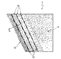
図1は、従来の光学装置1の一部の画像の図を示し、画像は透過型電子顕微鏡(TEM)により取られたものである。光学装置1は、普通はInPで作られたnクラッド部11を有する。光学装置1は図では、例えば基板(nクラッド部)11の上で成長させられたGaInAsPまたはAlGaInAsで作られたいくつかのバリアおよび閉じ込め層12を有する。成長の方向は、矢印Aによって示されている。量子ドット層13は、それぞれのバリア層12の間に設けられている。図から明らかに分かるように、量子ドット層13のそれぞれの表面、およびバリア層12の表面は粗い(円滑ではない)。さらに、表面の形状の粗さは、下側の量子ドット層から上側の量子ドット層まで(矢印Aの方向に)移動するときに大きくなる。図では、装置の上表面14は、基板11の下表面と比べてより高いレベルの粗さを示すことを観察することができる。これは主に、層の成長過程中に、(粗い)量子ドット層13の上側インターフェイスまたは表面が、バリア層12の被着中に平滑化されなかったという事実によるものである。粗さは普通、成長中に前の量子ドット層によって生じた歪場に対する、バリア材料、例えばGaInAsPの高い感度によるものである。大きな粗さの結果、量子ドット層13の厚さはまた、図1で矢印Aの方向で観察することができるように、下側量子ドット層から上側量子ドット層まで大きくなる。したがって、歪場は遮断されず、スタックの数が多くなると共にその影響が大きくなる。既に上に述べたように、歪場は密接して積み重ねられた構造が望ましい場合に悪影響を及ぼす。
FIG. 1 shows a partial image of a conventional optical device 1, which was taken with a transmission electron microscope (TEM). The optical device 1 has an n-clad
図2は、本発明の一実施形態による光学装置の一部の画像の図を示している。画像自体は、透過型電子顕微鏡(TEM)により取られたものである。この画像は、例として単に示されたものであり、本発明の範囲を限定するものとして解釈すべきでないことに留意されたい。 FIG. 2 shows an image view of a portion of an optical device according to an embodiment of the invention. The image itself was taken with a transmission electron microscope (TEM). It should be noted that this image is merely shown as an example and should not be construed as limiting the scope of the invention.
図2では、それぞれのバリア層12の間に置かれた量子ドット層13aおよび13bのスタックが示されており、成長の方向は矢印Aで示されている。 In FIG. 2, a stack of quantum dot layers 13a and 13b placed between each barrier layer 12 is shown, and the direction of growth is indicated by arrow A.
本発明によると、スペーサ層15はそれぞれのバリア層12上に被着される。スペーサ層は、歪場に対する感度が低い材料である、または少なくとも、バリア層12の粗い表面上に被着されるときに歪場の影響を実質的に遮断することが可能である。上にさらに述べたように、InPなどの2成分材料は、この目的で使用可能な材料の例である。実際の慣習では、スペーサとして使用される材料は、理想的な状態を現実の材料で得ることができないので、歪場に対して完全感度が低くなっていることはできないことに留意されたい。したがって、本明細書では、歪場に対する「感度が低い」材料への言及は、相対的な用語で、歪場の影響を実質的に遮断することができる材料であると理解すべきものである。
According to the present invention, the
図2に示すように、量子ドット層13aは粗い表面16aを呈する。バリア層12は、被着が終了した場合に、量子ドット層の粗さにより粗い表面16bを形成する量子ドット層13aの上に被着される。次に、スペーサ層15はバリア層12の表面16bの上に被着される。スペーサ層15は歪場に対する感度が低いので、スペーサ層15の得られる表面17aはほぼ円滑である(粗さがない)。次のバリア層、バリア層12はしたがって、この円滑な表面17aの上で成長される。その結果、歪場が避けられ、バリア層12に対する円滑な上表面17bが得られる。
As shown in FIG. 2, the quantum dot layer 13a exhibits a rough surface 16a. When the deposition is completed, the barrier layer 12 is deposited on the quantum dot layer 13a that forms a
したがって、中間スペーサ層15が成長最前部上に円滑な表面を有するので、比較的薄いバリア層12をその上に成長させることが可能となり、それによって相対的にかなりの数の量子ドット層を積み重ねることができる。実験により、最大20の量子ドット層のスタックでさえも、装置構造に実質的な転位を生じさせることはないことが示された。
Thus, since the
実際の実験では、それぞれ1nmの厚さを有する2つのバリア間に置かれた、InP材料である3nmのスペーサ層厚さを備えた10の量子ドット層のスタックを有するサンプル装置が作られた。装置は、単一の横モード・レーザ技術を使用して処理された。その結果、約50mAの閾値電流ITh、および約0.1W/A毎ファセットの外部効率(W/A毎ファセットは、装置内に投入される、アンペアでの電流に対するワットでの出力の閾値を示す装置の効率である)が示された。したがって、実験により、約5nmの分離、すなわちスペーサ層厚さの3nmプラス、非放射欠陥を生じさせることなく10の量子ドット層のそれぞれ1nmの厚さを有する、スペーサ層の両側の2つのバリアに対応する2nmの密接な積み重ねを達成することが示された。 In an actual experiment, a sample device was fabricated having a stack of 10 quantum dot layers with a spacer layer thickness of 3 nm, which is InP material, placed between two barriers each having a thickness of 1 nm. The device was processed using a single transverse mode laser technique. As a result, a threshold current I Th of about 50 mA and an external efficiency of about 0.1 W / A per facet (W / A facet is the threshold of power output in watts relative to the current in amperes injected into the device. The efficiency of the device shown). Thus, experiments have shown that two barriers on either side of the spacer layer have a separation of about 5 nm, ie, 3 nm of the spacer layer thickness plus 1 nm each of the 10 quantum dot layers without causing non-radiative defects. It was shown to achieve a corresponding close stack of 2 nm.
本発明によって提案される解決法は、スタックの材料品質を低下させることなく密接に積み重ねられた量子ドット層を備えた光学装置の製造を可能にする重要な利点を提供する。その結果、潜在的な量子ドット・ベース装置は、低いタイミング・ジッタ、大きな光学帯域幅を呈する関連した利点で、偏光感度の低い動作に適合するようになる。このような装置を提供することによって、光ファイバ通信の応用例に対して、上に記したように、これらの装置の他の潜在的に有用な特徴を利用することが可能になる。 The solution proposed by the present invention provides an important advantage that allows the production of optical devices with closely stacked quantum dot layers without degrading the material quality of the stack. As a result, potential quantum dot based devices are adapted for low polarization sensitivity operation with the associated advantages of low timing jitter and large optical bandwidth. By providing such devices, it is possible to take advantage of other potentially useful features of these devices, as noted above, for fiber optic communications applications.
本発明によって提案される解決法で、改善された特徴を有する、高温挙動を備えた広帯域半導体光増幅器(SOA)を製造することができる。別の利点は、低チャープ増幅を得ることができるようになることである。 With the solution proposed by the present invention, it is possible to produce broadband semiconductor optical amplifiers (SOA) with improved characteristics and with high temperature behavior. Another advantage is that low chirp amplification can be obtained.
本発明の装置は、これに限らないが、クロック修復、光増幅、波長変換または信号処理などの光信号処理を行うあらゆるユニットで使用することができる。 The apparatus of the present invention can be used in any unit that performs optical signal processing such as, but not limited to, clock recovery, optical amplification, wavelength conversion, or signal processing.
さらに、請求する手段に対応する構造のリストは排他的なものではなく、当業者は本発明の範囲から逸脱することなく同等の構造を言及した構造に換えることができることが分かることに留意するものとする。 Furthermore, it is noted that the list of structures corresponding to the claimed means is not exclusive and it will be understood that one skilled in the art can substitute structures referring to equivalent structures without departing from the scope of the present invention. And
Claims (18)
Applications Claiming Priority (2)
| Application Number | Priority Date | Filing Date | Title |
|---|---|---|---|
| EP08305281.1A EP2136445B1 (en) | 2008-06-19 | 2008-06-19 | An optical device having a quantum-dot structure |
| EP08305281.1 | 2008-06-19 |
Publications (2)
| Publication Number | Publication Date |
|---|---|
| JP2010004045A true JP2010004045A (en) | 2010-01-07 |
| JP5384217B2 JP5384217B2 (en) | 2014-01-08 |
Family
ID=40011281
Family Applications (1)
| Application Number | Title | Priority Date | Filing Date |
|---|---|---|---|
| JP2009146068A Expired - Fee Related JP5384217B2 (en) | 2008-06-19 | 2009-06-19 | Optical device having quantum dot structure |
Country Status (5)
| Country | Link |
|---|---|
| US (1) | US7968863B2 (en) |
| EP (1) | EP2136445B1 (en) |
| JP (1) | JP5384217B2 (en) |
| KR (1) | KR20090132529A (en) |
| CN (1) | CN101609960B (en) |
Families Citing this family (5)
| Publication number | Priority date | Publication date | Assignee | Title |
|---|---|---|---|---|
| EP2136445B1 (en) * | 2008-06-19 | 2016-04-13 | Alcatel Lucent | An optical device having a quantum-dot structure |
| FR2967905B1 (en) * | 2010-11-25 | 2013-07-12 | Oreal | PROCESS FOR TREATING TRANSPIRATION USING A CARBONYL COMPOUND WHICH CAN BE REACTED ACCORDING TO THE MAILLARD REACTION |
| CN107431111A (en) * | 2014-12-26 | 2017-12-01 | Ns材料株式会社 | Wavelength converting member and its manufacture method |
| US10236659B2 (en) | 2017-04-04 | 2019-03-19 | Rochester Institute Of Technology | Mode-locked lasers on silicon by palladium bonding and methods therefor |
| CN108983446B (en) * | 2017-06-01 | 2021-04-06 | Tcl科技集团股份有限公司 | Light intensity modulator |
Citations (3)
| Publication number | Priority date | Publication date | Assignee | Title |
|---|---|---|---|---|
| WO2004055900A1 (en) * | 2002-12-16 | 2004-07-01 | Japan Science And Technology Agency | Semiconductor multilayer structure having inhomogeneous quantum dots, light-emitting diode using same, semiconductor laser diode, semiconductor optical amplifier, and method for manufacturing them |
| JP2005072338A (en) * | 2003-08-26 | 2005-03-17 | Fujitsu Ltd | Optical semiconductor device and its manufacturing method |
| JP2007157975A (en) * | 2005-12-05 | 2007-06-21 | Fujitsu Ltd | Manufacturing method of semiconductor device |
Family Cites Families (4)
| Publication number | Priority date | Publication date | Assignee | Title |
|---|---|---|---|---|
| JP3468866B2 (en) | 1994-09-16 | 2003-11-17 | 富士通株式会社 | Semiconductor device using three-dimensional quantum confinement |
| JP3672678B2 (en) | 1996-04-05 | 2005-07-20 | 富士通株式会社 | Quantum semiconductor device and manufacturing method thereof |
| JP4952005B2 (en) * | 2006-03-07 | 2012-06-13 | 富士通株式会社 | Semiconductor device and manufacturing method thereof |
| EP2136445B1 (en) * | 2008-06-19 | 2016-04-13 | Alcatel Lucent | An optical device having a quantum-dot structure |
-
2008
- 2008-06-19 EP EP08305281.1A patent/EP2136445B1/en not_active Not-in-force
-
2009
- 2009-06-11 US US12/457,463 patent/US7968863B2/en not_active Expired - Fee Related
- 2009-06-18 KR KR1020090054356A patent/KR20090132529A/en not_active Application Discontinuation
- 2009-06-18 CN CN200910147531.2A patent/CN101609960B/en not_active Expired - Fee Related
- 2009-06-19 JP JP2009146068A patent/JP5384217B2/en not_active Expired - Fee Related
Patent Citations (3)
| Publication number | Priority date | Publication date | Assignee | Title |
|---|---|---|---|---|
| WO2004055900A1 (en) * | 2002-12-16 | 2004-07-01 | Japan Science And Technology Agency | Semiconductor multilayer structure having inhomogeneous quantum dots, light-emitting diode using same, semiconductor laser diode, semiconductor optical amplifier, and method for manufacturing them |
| JP2005072338A (en) * | 2003-08-26 | 2005-03-17 | Fujitsu Ltd | Optical semiconductor device and its manufacturing method |
| JP2007157975A (en) * | 2005-12-05 | 2007-06-21 | Fujitsu Ltd | Manufacturing method of semiconductor device |
Also Published As
| Publication number | Publication date |
|---|---|
| KR20090132529A (en) | 2009-12-30 |
| US20090315019A1 (en) | 2009-12-24 |
| EP2136445A1 (en) | 2009-12-23 |
| CN101609960B (en) | 2014-10-15 |
| JP5384217B2 (en) | 2014-01-08 |
| EP2136445B1 (en) | 2016-04-13 |
| CN101609960A (en) | 2009-12-23 |
| US7968863B2 (en) | 2011-06-28 |
Similar Documents
| Publication | Publication Date | Title |
|---|---|---|
| Lu et al. | CW lasing of current injection blue GaN-based vertical cavity surface emitting laser | |
| JP3854560B2 (en) | Quantum optical semiconductor device | |
| Sugawara et al. | Quantum dot devices: Handling the heat | |
| JP4983790B2 (en) | Optical semiconductor device and manufacturing method thereof | |
| JP5384217B2 (en) | Optical device having quantum dot structure | |
| EP0647001B1 (en) | Polarization insensitive semiconductor optical amplifier | |
| JP2015533025A (en) | Semiconductor device | |
| WO2013118248A1 (en) | Light-emitting element | |
| JP2010232424A (en) | Semiconductor optical amplifier, and optical module | |
| Kawashima et al. | GaN-based surface-emitting laser with two-dimensional photonic crystal acting as distributed-feedback grating and optical cladding | |
| JP5374894B2 (en) | Semiconductor optical amplifier, manufacturing method thereof, and semiconductor optical integrated device | |
| Lodahl et al. | A deterministic source of single photons | |
| WO2017210300A1 (en) | Integration of direct-bandgap optically active devices on indirect-bandgap-based substrates | |
| EP0545262B1 (en) | Strained quantum well laser diode | |
| JP2004087749A (en) | Semiconductor light device having quantum dot | |
| JP2008091420A (en) | Method of manufacturing quantum dot optical semiconductor element | |
| Cao et al. | Silicon-based three-dimensional photonic crystal nanocavity laser with InAs quantum-dot gain | |
| JP2007311463A (en) | Quantum dot semiconductor device | |
| JP6437869B2 (en) | Semiconductor laser | |
| JP2008216883A (en) | Photonic crystal resonator, photon pair producing apparatus, and photonic phase modulator | |
| Brenot et al. | Quantum dots semiconductor optical amplifier with a-3dB bandwidth of up to 120 nm in semi-cooled operation | |
| JP3230576B2 (en) | Semiconductor light emitting device | |
| JP3816924B2 (en) | Semiconductor waveguide type light control element | |
| JPH1090738A (en) | Non-linear optical device | |
| Sugawara et al. | Handling the heat |
Legal Events
| Date | Code | Title | Description |
|---|---|---|---|
| A977 | Report on retrieval |
Free format text: JAPANESE INTERMEDIATE CODE: A971007 Effective date: 20120227 |
|
| A131 | Notification of reasons for refusal |
Free format text: JAPANESE INTERMEDIATE CODE: A131 Effective date: 20120319 |
|
| A601 | Written request for extension of time |
Free format text: JAPANESE INTERMEDIATE CODE: A601 Effective date: 20120619 |
|
| A602 | Written permission of extension of time |
Free format text: JAPANESE INTERMEDIATE CODE: A602 Effective date: 20120622 |
|
| RD04 | Notification of resignation of power of attorney |
Free format text: JAPANESE INTERMEDIATE CODE: A7424 Effective date: 20120710 |
|
| A521 | Request for written amendment filed |
Free format text: JAPANESE INTERMEDIATE CODE: A523 Effective date: 20120919 |
|
| A02 | Decision of refusal |
Free format text: JAPANESE INTERMEDIATE CODE: A02 Effective date: 20130402 |
|
| A521 | Request for written amendment filed |
Free format text: JAPANESE INTERMEDIATE CODE: A523 Effective date: 20130802 |
|
| A911 | Transfer to examiner for re-examination before appeal (zenchi) |
Free format text: JAPANESE INTERMEDIATE CODE: A911 Effective date: 20130809 |
|
| TRDD | Decision of grant or rejection written | ||
| A01 | Written decision to grant a patent or to grant a registration (utility model) |
Free format text: JAPANESE INTERMEDIATE CODE: A01 Effective date: 20130903 |
|
| A61 | First payment of annual fees (during grant procedure) |
Free format text: JAPANESE INTERMEDIATE CODE: A61 Effective date: 20131002 |
|
| R150 | Certificate of patent or registration of utility model |
Free format text: JAPANESE INTERMEDIATE CODE: R150 Ref document number: 5384217 Country of ref document: JP Free format text: JAPANESE INTERMEDIATE CODE: R150 |
|
| R250 | Receipt of annual fees |
Free format text: JAPANESE INTERMEDIATE CODE: R250 |
|
| R250 | Receipt of annual fees |
Free format text: JAPANESE INTERMEDIATE CODE: R250 |
|
| R250 | Receipt of annual fees |
Free format text: JAPANESE INTERMEDIATE CODE: R250 |
|
| S111 | Request for change of ownership or part of ownership |
Free format text: JAPANESE INTERMEDIATE CODE: R313113 |
|
| S531 | Written request for registration of change of domicile |
Free format text: JAPANESE INTERMEDIATE CODE: R313531 |
|
| R371 | Transfer withdrawn |
Free format text: JAPANESE INTERMEDIATE CODE: R371 |
|
| S111 | Request for change of ownership or part of ownership |
Free format text: JAPANESE INTERMEDIATE CODE: R313113 |
|
| S531 | Written request for registration of change of domicile |
Free format text: JAPANESE INTERMEDIATE CODE: R313531 |
|
| R350 | Written notification of registration of transfer |
Free format text: JAPANESE INTERMEDIATE CODE: R350 |
|
| R250 | Receipt of annual fees |
Free format text: JAPANESE INTERMEDIATE CODE: R250 |
|
| R250 | Receipt of annual fees |
Free format text: JAPANESE INTERMEDIATE CODE: R250 |
|
| LAPS | Cancellation because of no payment of annual fees |