JP2009543355A - Cluster tools for advanced front-end processing - Google Patents
Cluster tools for advanced front-end processing Download PDFInfo
- Publication number
- JP2009543355A JP2009543355A JP2009518542A JP2009518542A JP2009543355A JP 2009543355 A JP2009543355 A JP 2009543355A JP 2009518542 A JP2009518542 A JP 2009518542A JP 2009518542 A JP2009518542 A JP 2009518542A JP 2009543355 A JP2009543355 A JP 2009543355A
- Authority
- JP
- Japan
- Prior art keywords
- substrate
- chamber
- processing
- support
- region
- Prior art date
- Legal status (The legal status is an assumption and is not a legal conclusion. Google has not performed a legal analysis and makes no representation as to the accuracy of the status listed.)
- Pending
Links
Images


Classifications
-
- H—ELECTRICITY
- H01—ELECTRIC ELEMENTS
- H01L—SEMICONDUCTOR DEVICES NOT COVERED BY CLASS H10
- H01L21/00—Processes or apparatus adapted for the manufacture or treatment of semiconductor or solid state devices or of parts thereof
- H01L21/67—Apparatus specially adapted for handling semiconductor or electric solid state devices during manufacture or treatment thereof; Apparatus specially adapted for handling wafers during manufacture or treatment of semiconductor or electric solid state devices or components ; Apparatus not specifically provided for elsewhere
- H01L21/677—Apparatus specially adapted for handling semiconductor or electric solid state devices during manufacture or treatment thereof; Apparatus specially adapted for handling wafers during manufacture or treatment of semiconductor or electric solid state devices or components ; Apparatus not specifically provided for elsewhere for conveying, e.g. between different workstations
- H01L21/67739—Apparatus specially adapted for handling semiconductor or electric solid state devices during manufacture or treatment thereof; Apparatus specially adapted for handling wafers during manufacture or treatment of semiconductor or electric solid state devices or components ; Apparatus not specifically provided for elsewhere for conveying, e.g. between different workstations into and out of processing chamber
- H01L21/67745—Apparatus specially adapted for handling semiconductor or electric solid state devices during manufacture or treatment thereof; Apparatus specially adapted for handling wafers during manufacture or treatment of semiconductor or electric solid state devices or components ; Apparatus not specifically provided for elsewhere for conveying, e.g. between different workstations into and out of processing chamber characterized by movements or sequence of movements of transfer devices
-
- H—ELECTRICITY
- H01—ELECTRIC ELEMENTS
- H01L—SEMICONDUCTOR DEVICES NOT COVERED BY CLASS H10
- H01L21/00—Processes or apparatus adapted for the manufacture or treatment of semiconductor or solid state devices or of parts thereof
- H01L21/67—Apparatus specially adapted for handling semiconductor or electric solid state devices during manufacture or treatment thereof; Apparatus specially adapted for handling wafers during manufacture or treatment of semiconductor or electric solid state devices or components ; Apparatus not specifically provided for elsewhere
-
- B—PERFORMING OPERATIONS; TRANSPORTING
- B08—CLEANING
- B08B—CLEANING IN GENERAL; PREVENTION OF FOULING IN GENERAL
- B08B7/00—Cleaning by methods not provided for in a single other subclass or a single group in this subclass
- B08B7/0035—Cleaning by methods not provided for in a single other subclass or a single group in this subclass by radiant energy, e.g. UV, laser, light beam or the like
- B08B7/0057—Cleaning by methods not provided for in a single other subclass or a single group in this subclass by radiant energy, e.g. UV, laser, light beam or the like by ultraviolet radiation
-
- C—CHEMISTRY; METALLURGY
- C23—COATING METALLIC MATERIAL; COATING MATERIAL WITH METALLIC MATERIAL; CHEMICAL SURFACE TREATMENT; DIFFUSION TREATMENT OF METALLIC MATERIAL; COATING BY VACUUM EVAPORATION, BY SPUTTERING, BY ION IMPLANTATION OR BY CHEMICAL VAPOUR DEPOSITION, IN GENERAL; INHIBITING CORROSION OF METALLIC MATERIAL OR INCRUSTATION IN GENERAL
- C23C—COATING METALLIC MATERIAL; COATING MATERIAL WITH METALLIC MATERIAL; SURFACE TREATMENT OF METALLIC MATERIAL BY DIFFUSION INTO THE SURFACE, BY CHEMICAL CONVERSION OR SUBSTITUTION; COATING BY VACUUM EVAPORATION, BY SPUTTERING, BY ION IMPLANTATION OR BY CHEMICAL VAPOUR DEPOSITION, IN GENERAL
- C23C16/00—Chemical coating by decomposition of gaseous compounds, without leaving reaction products of surface material in the coating, i.e. chemical vapour deposition [CVD] processes
- C23C16/44—Chemical coating by decomposition of gaseous compounds, without leaving reaction products of surface material in the coating, i.e. chemical vapour deposition [CVD] processes characterised by the method of coating
- C23C16/54—Apparatus specially adapted for continuous coating
-
- H—ELECTRICITY
- H01—ELECTRIC ELEMENTS
- H01L—SEMICONDUCTOR DEVICES NOT COVERED BY CLASS H10
- H01L21/00—Processes or apparatus adapted for the manufacture or treatment of semiconductor or solid state devices or of parts thereof
- H01L21/02—Manufacture or treatment of semiconductor devices or of parts thereof
- H01L21/04—Manufacture or treatment of semiconductor devices or of parts thereof the devices having at least one potential-jump barrier or surface barrier, e.g. PN junction, depletion layer or carrier concentration layer
- H01L21/18—Manufacture or treatment of semiconductor devices or of parts thereof the devices having at least one potential-jump barrier or surface barrier, e.g. PN junction, depletion layer or carrier concentration layer the devices having semiconductor bodies comprising elements of Group IV of the Periodic System or AIIIBV compounds with or without impurities, e.g. doping materials
- H01L21/30—Treatment of semiconductor bodies using processes or apparatus not provided for in groups H01L21/20 - H01L21/26
- H01L21/302—Treatment of semiconductor bodies using processes or apparatus not provided for in groups H01L21/20 - H01L21/26 to change their surface-physical characteristics or shape, e.g. etching, polishing, cutting
-
- H—ELECTRICITY
- H01—ELECTRIC ELEMENTS
- H01L—SEMICONDUCTOR DEVICES NOT COVERED BY CLASS H10
- H01L21/00—Processes or apparatus adapted for the manufacture or treatment of semiconductor or solid state devices or of parts thereof
- H01L21/67—Apparatus specially adapted for handling semiconductor or electric solid state devices during manufacture or treatment thereof; Apparatus specially adapted for handling wafers during manufacture or treatment of semiconductor or electric solid state devices or components ; Apparatus not specifically provided for elsewhere
- H01L21/67005—Apparatus not specifically provided for elsewhere
- H01L21/67011—Apparatus for manufacture or treatment
- H01L21/67098—Apparatus for thermal treatment
- H01L21/67115—Apparatus for thermal treatment mainly by radiation
-
- H—ELECTRICITY
- H01—ELECTRIC ELEMENTS
- H01L—SEMICONDUCTOR DEVICES NOT COVERED BY CLASS H10
- H01L21/00—Processes or apparatus adapted for the manufacture or treatment of semiconductor or solid state devices or of parts thereof
- H01L21/67—Apparatus specially adapted for handling semiconductor or electric solid state devices during manufacture or treatment thereof; Apparatus specially adapted for handling wafers during manufacture or treatment of semiconductor or electric solid state devices or components ; Apparatus not specifically provided for elsewhere
- H01L21/67005—Apparatus not specifically provided for elsewhere
- H01L21/67011—Apparatus for manufacture or treatment
- H01L21/67155—Apparatus for manufacturing or treating in a plurality of work-stations
- H01L21/6719—Apparatus for manufacturing or treating in a plurality of work-stations characterized by the construction of the processing chambers, e.g. modular processing chambers
-
- H—ELECTRICITY
- H01—ELECTRIC ELEMENTS
- H01L—SEMICONDUCTOR DEVICES NOT COVERED BY CLASS H10
- H01L21/00—Processes or apparatus adapted for the manufacture or treatment of semiconductor or solid state devices or of parts thereof
- H01L21/67—Apparatus specially adapted for handling semiconductor or electric solid state devices during manufacture or treatment thereof; Apparatus specially adapted for handling wafers during manufacture or treatment of semiconductor or electric solid state devices or components ; Apparatus not specifically provided for elsewhere
- H01L21/67005—Apparatus not specifically provided for elsewhere
- H01L21/67011—Apparatus for manufacture or treatment
- H01L21/67155—Apparatus for manufacturing or treating in a plurality of work-stations
- H01L21/67196—Apparatus for manufacturing or treating in a plurality of work-stations characterized by the construction of the transfer chamber
-
- H—ELECTRICITY
- H01—ELECTRIC ELEMENTS
- H01L—SEMICONDUCTOR DEVICES NOT COVERED BY CLASS H10
- H01L21/00—Processes or apparatus adapted for the manufacture or treatment of semiconductor or solid state devices or of parts thereof
- H01L21/67—Apparatus specially adapted for handling semiconductor or electric solid state devices during manufacture or treatment thereof; Apparatus specially adapted for handling wafers during manufacture or treatment of semiconductor or electric solid state devices or components ; Apparatus not specifically provided for elsewhere
- H01L21/67005—Apparatus not specifically provided for elsewhere
- H01L21/67242—Apparatus for monitoring, sorting or marking
- H01L21/67253—Process monitoring, e.g. flow or thickness monitoring
Abstract
本発明の態様は、一般的に、基板を処理し、基板において遂行されたプロセスの結果を分析するように適応される複数のチャンバ処理システムを使用して基板を処理する装置及び方法を提供する。本発明の1つの態様において、1つ以上の分析ステップ及び/又は前クリーニングステップを使用して、装置の歩留りに対するキュータイムの影響を減少させる。本発明の1つの態様において、システムコントローラ及び1つ以上の分析チャンバを使用して、プロセスチャンバレシピ及び/又はプロセスシーケンスを監視及び制御して、形成された装置の欠陥及び装置性能の変化の問題による基板の廃棄を減少させる。また、本発明の実施形態は、一般的に、種々の用途に使用される半導体装置を繰り返し高い信頼性で形成するための方法及びシステムを提供する。
【選択図】 図15Aspects of the present invention generally provide an apparatus and method for processing a substrate using a plurality of chamber processing systems adapted to process the substrate and analyze the results of processes performed on the substrate. . In one aspect of the invention, one or more analysis steps and / or pre-cleaning steps are used to reduce the effect of cue time on device yield. In one aspect of the present invention, a system controller and one or more analysis chambers are used to monitor and control process chamber recipes and / or process sequences to form device defects and device performance change issues. Reduces substrate disposal due to Embodiments of the present invention also generally provide a method and system for repeatedly and reliably forming semiconductor devices used in various applications.
[Selection] FIG.
Description
発明の分野
[0001]本発明の実施形態は、一般に、基板処理モジュール、基板準備チャンバ、及び/又はプロセス検証及び分析チャンバを含む処理シーケンスを遂行するように構成された一体型処理システムに関する。
Field of Invention
[0001] Embodiments of the present invention generally relate to an integrated processing system configured to perform a processing sequence including a substrate processing module, a substrate preparation chamber, and / or a process verification and analysis chamber.
関連技術の説明
[0002]半導体装置を形成するプロセスは、通常、制御された処理環境で基板(例えば、半導体ウェハ)を処理する能力を有する複数のチャンバ処理システム(例えば、クラスターツール)で行われる。典型的な制御された処理環境は、メインフレームを有するシステムを含み、メインフレームは、これに接続された複数の真空処理チャンバとロードロックとの間で基板を搬送する基板移送ロボットを収容している。制御された処理環境は、基板移送中及び種々の基板処理ステップの実行中に基板表面の汚染を最小にすることを含む多数の利益を有する。従って、制御された環境内での処理により、発生する欠陥の数が減少されると共に、装置の歩留りが改善される。
Explanation of related technology
[0002] Processes for forming semiconductor devices are typically performed in multiple chamber processing systems (eg, cluster tools) that have the ability to process substrates (eg, semiconductor wafers) in a controlled processing environment. A typical controlled processing environment includes a system having a main frame that houses a substrate transfer robot that transfers substrates between a plurality of vacuum processing chambers connected thereto and a load lock. Yes. A controlled processing environment has a number of benefits including minimizing contamination of the substrate surface during substrate transfer and during various substrate processing steps. Thus, processing in a controlled environment reduces the number of defects that occur and improves device yield.
[0003]基板製造プロセスの有効性は、装置の歩留り及び所有費(CoO)の2つの関連した重要なファクタによってしばしば測定される。これらのファクタが重要であるのは、電子装置を製造するコスト、ひいては、市場における装置製造者の競争力に直接影響するからである。CoOは、多数のファクタによって影響されるが、装置のプロセスシーケンス中に形成される装置の歩留り、及び基板のスループット又は単に1時間当りの基板の枚数によって大きく影響される。プロセスシーケンスとは、一般的に、クラスターツール内の1つ以上の処理チャンバにおいて完了される装置製造ステップ又はプロセスレシピステップのシーケンスとして定義される。プロセスシーケンスは、一般的に、種々の基板(又はウェハ)製造処理ステップを含んでもよい。 [0003] The effectiveness of a substrate manufacturing process is often measured by two related important factors: device yield and cost of ownership (CoO). These factors are important because they directly affect the cost of manufacturing the electronic device and thus the competitiveness of the device manufacturer in the market. CoO is affected by a number of factors, but is greatly influenced by the yield of the device formed during the process sequence of the device, and the substrate throughput or simply the number of substrates per hour. A process sequence is generally defined as a sequence of device manufacturing steps or process recipe steps that are completed in one or more processing chambers within a cluster tool. A process sequence may generally include various substrate (or wafer) manufacturing process steps.
[0004]半導体装置のサイズを縮小して装置の処理速度を改善すると共に装置による熱の発生を減少するための業界の後押しで、縮小のためのプロセス変化に対する業界の寛容度が生じた。半導体装置の縮小するサイズと、絶えず高まる装置性能要件のために、装置製造プロセスの均一性及び反復性の許容変化量が著しく減少した。装置性能の変化及び反復性に影響し得る1つのファクタは、「キュータイム(待ち時間、queuetime)」として知られている。キュータイムとは、一般的に、基板に対して第1のプロセスが完了した後に、製造される装置の性能への何らかの悪影響を防止するために基板に対して第2のプロセスを完了しなければならなくなるまで、基板を大気又は他の汚染物に露出させることのできる時間として定義される。許容キュータイムに近いか又はそれより長い時間中、基板が大気又は他の汚染源に露出される場合には、第1の層と第2の層との間の界面の汚染により装置の性能に影響が及ぶことがある。それ故、基板を大気又は他の汚染源に露出させることを含むプロセスシーケンスの場合に、基板をこれらの汚染源に露出させる時間を、装置の性能変化を防止するように制御するか又は最小にしなければならない。それ故、有用な電子装置製造プロセスは、均一で且つ反復性のあるプロセス結果を与え、汚染物の影響を最小にすると共に、基板処理シーケンスに使用するために考慮されるべき希望のスループットを満足しなければならない。 [0004] Industry boosts to reduce the size of semiconductor devices to improve the processing speed of the devices and reduce the heat generation by the devices have created an industry tolerance for process changes due to the reduction. Due to the shrinking size of semiconductor devices and ever-increasing device performance requirements, the tolerances for device manufacturing process uniformity and repeatability have been significantly reduced. One factor that can affect device performance changes and repeatability is known as "queue time". The cue time generally means that after the first process is completed on the substrate, the second process must be completed on the substrate to prevent any adverse effects on the performance of the manufactured device. Defined as the time allowed for the substrate to be exposed to the atmosphere or other contaminants until no longer exists. Contamination of the interface between the first and second layers affects the performance of the device if the substrate is exposed to the atmosphere or other sources for a time near or longer than the allowable cue time. May reach. Therefore, in the case of a process sequence that involves exposing the substrate to the atmosphere or other sources of contamination, the time that the substrate is exposed to these sources of contamination must be controlled or minimized to prevent changes in device performance. Don't be. Therefore, a useful electronic device manufacturing process provides uniform and repeatable process results, minimizes the effects of contaminants, and satisfies the desired throughput to be considered for use in substrate processing sequences. Must.
[0005]半導体装置の製造者は、誤って処理された基板、装置欠陥、又は形成された装置の性能変化による基板の廃棄によって生じるCoOの問題を軽減するよう試みて、著しい量の時間を費やしている。典型的に、誤って処理された基板、装置欠陥、及び/又は装置性能の変化は、処理シーケンスにおける1つ以上の処理チャンバ内のプロセスドリフト、システム又はプロセスチャンバに見られる汚染、或いは基板又は基板の層のスタート条件の変化によって引き起こされる。プロセス結果が希望のプロセス窓内に入るよう保証するために使用される従来の方法は、1つ以上のオフライン分析技術をしばしば使用している。オフラインテスト及び分析技術は、処理シーケンス及び処理環境から1つ以上の基板を周期的に取り出すか又は一定に頻繁に取り出すことを必要とし、これら基板は、次いで、テスト環境へ送り込まれる。従って、基板の移送及び点検中に生産の流れが実際上妨げられる。その結果、従来の計測点検方法は、チップ製造に関連したオーバーヘッド時間を著しく増加することになる。更に、このような点検方法は、スループットへの否定的な影響のために周期的にサンプリングするように行われるだけであるので、汚染された多くの基板が点検せずに処理されて、欠陥装置が製造されることになる。基板が所与のバッチから再分配される場合には問題が複合化されて、汚染源を追跡することが困難になる。従って、膜の応力、膜の組成、粒子、処理欠陥、等を含む選択された重要な装置特性に対して検査し、次いで、処理条件をオンザフライで調整して、その後に処理される基板に発生する問題を是正することのできる一体型計測及びプロセス点検システムが要望される。このような点検は、基板処理の前、基板処理中、及び基板処理の後に行って、基板の前処理及び後処理条件をリアルタイムで決定できるのが好ましい。 [0005] Semiconductor device manufacturers spend a significant amount of time trying to mitigate CoO problems caused by disposal of substrates due to misprocessed substrates, device defects, or performance changes in the formed devices. ing. Typically, misprocessed substrates, device defects, and / or changes in device performance are due to process drift within one or more processing chambers in the processing sequence, contamination found in the system or process chamber, or substrate or substrate. Caused by changes in the starting conditions of the layers. Conventional methods used to ensure that process results fall within the desired process window often use one or more off-line analysis techniques. Off-line testing and analysis techniques require periodic or constant frequent removal of one or more substrates from the processing sequence and processing environment, which are then fed into the test environment. Thus, the production flow is effectively hindered during substrate transfer and inspection. As a result, the conventional measurement and inspection method significantly increases the overhead time associated with chip manufacture. Furthermore, since such inspection methods are only performed to sample periodically due to negative impact on throughput, many contaminated substrates are processed without inspection, resulting in defective devices. Will be manufactured. The problem is compounded when the substrate is redistributed from a given batch, making it difficult to track the source of contamination. Therefore, inspect for selected critical equipment properties including film stress, film composition, particles, processing defects, etc., then adjust the processing conditions on-the-fly and then occur on the substrate being processed There is a need for an integrated measurement and process inspection system that can correct these problems. Such inspection is preferably performed before substrate processing, during substrate processing, and after substrate processing, so that pre-processing and post-processing conditions of the substrate can be determined in real time.
[0006]それ故、必要な装置性能目標を満足させ、システムのスループットを高め、ひいては、プロセスシーケンスのCoOを減少できるように基板を処理することのできるシステム、方法及び装置が要望される。 [0006] Therefore, there is a need for a system, method, and apparatus that can process a substrate to meet required device performance goals, increase system throughput, and thus reduce the CoO of a process sequence.
[0007]本発明は、一般に、ロボットが配設された移送領域を形成する1つ以上の壁と、移送領域内に配設されて、基板の表面の特性を測定するように適応される第1の支援チャンバと、移送領域に連通する基板処理チャンバとを備えた基板処理装置を提供する。 [0007] The present invention is generally adapted to measure one or more walls forming a transfer region in which a robot is disposed and a surface property of the substrate disposed in the transfer region. There is provided a substrate processing apparatus including one support chamber and a substrate processing chamber communicating with a transfer region.
[0008]本発明の実施形態は、更に、ロボットが配設された移送領域を形成する1つ以上の壁と、移送領域に連通する1つ以上の基板処理チャンバと、ロボットに連通する支援チャンバであって、基板の領域の特性を測定するように適応される支援チャンバと、移送領域に連通する基板処理チャンバと、この基板処理チャンバ内で処理ステップを遂行する前に基板の表面を準備するように適応される前クリーニングチャンバとを備えた基板処理装置を提供する。 [0008] Embodiments of the present invention further include one or more walls forming a transfer area in which the robot is disposed, one or more substrate processing chambers in communication with the transfer area, and an assistance chamber in communication with the robot. A support chamber adapted to measure characteristics of a region of the substrate, a substrate processing chamber in communication with the transfer region, and preparing a surface of the substrate prior to performing a processing step in the substrate processing chamber A substrate processing apparatus having a pre-cleaning chamber adapted to the above is provided.
[0009]本発明の実施形態は、更に、クラスターツールで半導体装置を形成する方法において、装置形成プロセスを使用して基板処理チャンバ内で基板の表面に装置特徴部を形成するステップと、支援チャンバ内に基板を位置付けて基板表面上の領域の特性を測定するステップと、その測定された特性をシステムコントローラに記憶された値と比較するステップと、この測定された特性とシステムコントローラに記憶された値との比較に基づいて装置形成プロセス中にプロセスパラメータを変更するステップとを備えた方法を提供する。 [0009] Embodiments of the present invention further include forming a device feature on a surface of a substrate in a substrate processing chamber using a device formation process in a method of forming a semiconductor device with a cluster tool, and a support chamber Positioning the substrate within and measuring the characteristics of the area on the substrate surface; comparing the measured characteristics with values stored in the system controller; and measuring the measured characteristics and stored in the system controller Changing a process parameter during the device formation process based on the comparison with the value.
[0010]本発明の実施形態は、更に、クラスターツールで半導体装置を形成する方法において、装置形成プロセスを使用して基板処理チャンバ内で基板の表面に装置特徴部を形成するステップと、クラスターツールの移送領域内に配設されたロボットを使用してその移送領域内に基板を位置付けるステップと、その移送領域内に位置付けられた基板の表面の特性を測定するステップと、その測定された特性をシステムコントローラに記憶された値と比較するステップと、この測定された特性とシステムコントローラに記憶された値との比較に基づいて装置形成プロセス中にプロセスパラメータを変更するステップとを備えた方法を提供する。 [0010] Embodiments of the present invention further include forming a device feature on a surface of a substrate in a substrate processing chamber using a device forming process in a method of forming a semiconductor device with a cluster tool; Positioning a substrate in the transfer area using a robot disposed in the transfer area, measuring the characteristics of the surface of the substrate positioned in the transfer area, and measuring the measured characteristics A method comprising: comparing with a value stored in a system controller; and changing process parameters during the device formation process based on a comparison of the measured characteristic with a value stored in the system controller. To do.
[0011]本発明の上述した特徴を詳細に理解できるように、簡単に概要を上述した本発明について、幾つかを添付図面に例示した実施形態を参照して以下に詳細に説明する。しかしながら、添付図面は、本発明の典型的な実施形態を例示するに過ぎず、それ故、本発明の範囲をそれに限定するものではなく、本発明は、等しく有効な他の実施形態も包含できることに注意されたい。 [0011] In order that the foregoing features of the invention may be understood in detail, the invention, briefly described above, will now be described in detail with reference to a few embodiments illustrated in the accompanying drawings. However, the accompanying drawings are merely illustrative of exemplary embodiments of the present invention, and therefore are not intended to limit the scope of the invention, and the invention may include other equally effective embodiments. Please be careful.
[0029]本発明は、一般的に、基板を処理して、基板上で行われたプロセスの結果を分析するように適応される複数チャンバ処理システム(例えば、クラスターツール)を使用して基板を処理するための装置及び方法を提供する。本発明の1つの態様においては、装置の歩留りに対するキュータイムの影響を減少するために、1つ以上の分析ステップ及び/又は前クリーニングステップが使用される。本発明の1つの態様においては、プロセスチャンバレシピ及び/又はプロセスシーケンスを監視し及び制御して、形成される装置の欠陥及び装置性能変化の問題による基板の廃棄を減少するために、システムコントローラ及び1つ以上の分析チャンバが使用される。また、本発明の実施形態は、一般的に、種々の用途に使用される半導体装置を繰り返し高い信頼性で形成するための方法及びシステムを提供する。本発明は、カリフォルニア州サンタクララのアプライドマテリアルズ社のFEP部門から入手できるセンチュラ(Centura)を参照して以下に例示する。 [0029] The present invention generally processes a substrate and processes the substrate using a multi-chamber processing system (eg, a cluster tool) adapted to analyze the results of processes performed on the substrate. An apparatus and method for processing are provided. In one aspect of the invention, one or more analysis steps and / or pre-cleaning steps are used to reduce the effect of cue time on device yield. In one aspect of the invention, a system controller and a process controller to monitor and control process chamber recipes and / or process sequences to reduce substrate disposal due to defects in formed device defects and device performance changes. One or more analysis chambers are used. Embodiments of the present invention also generally provide a method and system for repeatedly and reliably forming semiconductor devices used in various applications. The invention is illustrated below with reference to Centura available from the FEP division of Applied Materials, Inc., Santa Clara, California.
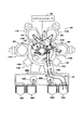
[0030]本発明の実施形態は、複数の単一基板処理チャンバ及び/又は複数のバッチ型処理チャンバ内で基板を処理する能力を有するクラスターツール構成で効果的に使用することができる。クラスターツールとは、電子装置を形成するのに使用される種々の処理ステップを遂行する複数のチャンバを備えたモジュラーシステムである。図1に示すように、クラスターツール100は複数の処理位置114A−114Fを含み、ここでは、処理チャンバ(図示せず)を中央の移送チャンバ110に装着することができ、この移送チャンバ110は、処理チャンバ間で基板を往復させるよう適応されるロボット113を収容する。移送チャンバ110の内部領域(例えば、図8の移送領域110C)は、典型的に真空状態に維持され、基板をあるチャンバから別のチャンバへ及び/又はクラスターツールのフロントエンドに位置付けられたロードロックチャンバへ往復させるところの中間領域をなす。真空状態は、典型的に、従来のラフポンプ、ルーツブロアー(RootsBlower)、従来のターボポンプ、従来のクライオポンプ又はその組合せのような1つ以上の真空ポンプ(図示せず)を使用することにより得られる。或いは又、移送チャンバ110の内部領域は、この内部領域に不活性ガスを連続的に送り込むことにより大気圧又はその付近に維持される不活性環境でもよい。図1は、本発明を効果的に使用できる電子装置処理のための典型的なクラスターツール100の平面図である。3つのこのようなプラットホームは、カリフォルニア州サンタクララのアプライドマテリアルズ社から全て入手できるセンチュラ(Centura)、エンデュラ(Endura)及びプロデューサ(Producer)システムである。1つの、このようなステージ型真空基板処理システムの詳細が、参考としてここに援用する、1993年2月16日発行のテプマン(Tepman)氏等による“Staged-VacuumSubstrate Processing System and Method”と題する米国特許第5,186,718号に開示されている。製造プロセスの特定のステップを遂行する目的でチャンバの厳密な配列及び組合せを変更することができる。
[0030] Embodiments of the present invention can be effectively used in cluster tool configurations with the ability to process substrates in multiple single substrate processing chambers and / or multiple batch type processing chambers. A cluster tool is a modular system with multiple chambers that perform various processing steps used to form an electronic device. As shown in FIG. 1, the
[0031]図2は、移送チャンバ110の位置114A、114B、144C及び114Dに基板処理チャンバ201、202、203及び204が各々装着されたクラスターツールの一実施形態を示す。本発明の態様によれば、クラスターツール100は、一般的に、複数のチャンバ及びロボットを備えると共に、クラスターツール100で遂行される種々の処理方法及びシーケンスを制御し実行するようにプログラムされたシステムコントローラ102が装備されるのが好ましい。複数のスリットバルブ(図示せず)を移送チャンバ110に追加して、位置114A−Fに装着されたプロセスチャンバの各々を選択的に分離し、処理シーケンス中に真空プロセスを遂行するように各チャンバを別々に排気することができる。本発明の幾つかの実施形態では、システムのコスト又は複雑さを低減するために、全ての位置114A−Fが処理チャンバで占有されるのではない。
[0031] FIG. 2 illustrates one embodiment of a cluster tool with
[0032]本発明の1つの態様では、基板処理チャンバ201−204の1つ以上は、基板処理シーケンスにおける1つ以上のステップ中に、シリコン(Si)、シリコンゲルマニウム(SiGe)、シリコン炭素(SiC)のような1つ以上の材料を含むエピタキシャル層を基板上に形成するのに使用できる従来のエピタキシャル(EPI)堆積チャンバでよい。EPIプロセスは、カリフォルニア州サンタクララに所在のアプライドマテリアルズ社から入手できるアプライドセンチュラEPIチャンバを使用して行うことができる。また、本発明の1つの態様では、基板処理チャンバ201−204の1つ以上は、基板処理シーケンスにおける1つ以上のステップ中に基板をアニールするのに使用できるRTPチャンバでよい。RTPプロセスは、カリフォルニア州サンタクララに所在のアプライドマテリアルズ社から商業的に入手できるRTPチャンバ(例えば、バンテージ・ラドオックス(VantageRadOx)RTP、バンテージ・ラジアンスプラス(Vantage RadiancePlus)RTP)及びその関連処理ハードウェアを使用して行うことができる。 [0032] In one aspect of the present invention, one or more of the substrate processing chambers 201-204 may include silicon (Si), silicon germanium (SiGe), silicon carbon (SiC) during one or more steps in the substrate processing sequence. And a conventional epitaxial (EPI) deposition chamber that can be used to form an epitaxial layer comprising one or more materials such as The EPI process can be performed using an Applied Centura EPI chamber available from Applied Materials, Inc., located in Santa Clara, California. Also, in one aspect of the invention, one or more of the substrate processing chambers 201-204 may be an RTP chamber that can be used to anneal the substrate during one or more steps in the substrate processing sequence. RTP processes are commercially available RTP chambers (eg, VantageRadOx RTP, Vantage RadiancePlus RTP) and related processing hardware from Applied Materials, Inc., located in Santa Clara, California. Can be done using wear.
[0033]本発明の別の態様では、基板処理チャンバ201−204の1つ以上は、金属(例えば、チタン、銅、タンタル)、半導体(例えば、シリコン、シリコンゲルマニウム、シリコン炭素、ゲルマニウム)、又は誘電体層(例えば、BlokTM、二酸化シリコン、SiN、HfOx、SiCN)を堆積するように適応される従来の化学気相堆積(CVD)チャンバでよい。このようなCVDプロセスチャンバは、例えば、カリフォルニア州サンタクララのアプライドマテリアルズ社から商業的に入手できるDXZTMチャンバ、ウルチマ(Ultima)HDP−CVDTMチャンバ、及びPRECISION 5000(登録商標)チャンバを含む。また、本発明の別の態様では、基板処理チャンバ201−204の1つ以上は、従来の物理気相堆積(PVD)チャンバでよい。このようなPVDプロセスチャンバは、例えば、カリフォルニア州サンタクララのアプライドマテリアルズ社から商業的に入手できるEndraTMPVD処理チャンバを含む。また、本発明の別の態様では、基板処理チャンバ201−204の1つ以上は、デカップル型プラズマ窒化(DPN)チャンバでよい。このようなDPNプロセスチャンバは、例えば、カリフォルニア州サンタクララのアプライドマテリアルズ社から商業的に入手できるCenturaTMDPNチャンバを含む。デカップル型プラズマ窒化プロセスを遂行するのに使用できる処理チャンバの一例が、参考としてここに全体を援用する2004年4月6日に出願された、共通に譲渡された米国特許出願第10/819,392号(US20040242021号として公告された)に説明されている。本発明の別の態様では、基板処理チャンバ201−204の1つ以上は、金属エッチング又は誘電体エッチングチャンバでよい。このような金属及び誘電体エッチングチャンバは、例えば、カリフォルニア州サンタクララのアプライドマテリアルズ社から商業的に入手できるCenturaTMアドバントエッジ(AdvantEdge)金属エッチングチャンバ及びCenturaTMeMAXチャンバを含む。 [0033] In another aspect of the invention, one or more of the substrate processing chambers 201-204 may be a metal (eg, titanium, copper, tantalum), a semiconductor (eg, silicon, silicon germanium, silicon carbon, germanium), or It may be a conventional chemical vapor deposition (CVD) chamber adapted to deposit a dielectric layer (eg, Blok ™ , silicon dioxide, SiN, HfO x , SiCN). Such CVD process chambers include, for example, the DXZ ™ chamber, the Ultima HDP-CVD ™ chamber, and the PRECISION 5000® chamber, commercially available from Applied Materials, Inc., Santa Clara, California. In another aspect of the invention, one or more of the substrate processing chambers 201-204 may be a conventional physical vapor deposition (PVD) chamber. Such PVD process chambers include, for example, the Endra ™ PVD process chamber commercially available from Applied Materials, Inc., Santa Clara, California. In another aspect of the invention, one or more of the substrate processing chambers 201-204 may be a decoupled plasma nitridation (DPN) chamber. Such DPN process chambers include, for example, the Centura ™ DPN chamber commercially available from Applied Materials, Inc., Santa Clara, California. An example of a processing chamber that can be used to perform a decoupled plasma nitridation process is described in commonly assigned US patent application Ser. No. 10/819, filed Apr. 6, 2004, which is hereby incorporated by reference in its entirety. 392 (published as US20040242021). In another aspect of the invention, one or more of the substrate processing chambers 201-204 may be a metal etch or dielectric etch chamber. Such metal and dielectric etch chambers include, for example, Centura TM Advan preparative edge (AdvantEdge) metal etch chamber and Centura TM eMAX chamber commercially available from Applied Materials, Inc. of Santa Clara, California.
[0034]図2を参照して上述したように、位置114A−Dの1つに装着される処理チャンバ201−204は、PVD、CVD(例えば、誘電体CVD、MCVD、MOCVD、EPI)、ALD、デカップル型プラズマ窒化(DPN)、急速熱処理(RTP)、又は乾式エッチングプロセスのような多数のプロセスを遂行して、基板の表面上に種々の装置特徴部を形成することができる。種々の装置特徴部は、層間誘電体層、ゲート誘電体層、ポリシリコンゲートの形成、ビア及びトレンチの形成、平坦化ステップ、及び接触部又はビアレベル相互接続部の堆積を含み得るが、これらに限定されない。一実施形態では、位置114E−114Fは、ガス抜き、オリエンテーション、冷却、等に適応されるサービスチャンバを含む。一実施形態では、処理シーケンスは、高Kキャパシタ構造体を形成するように適応され、この場合、処理チャンバ201−204は、DPNチャンバ、ポリシリコンを堆積できるCVDチャンバ、及び/又はチタン、タングステン、タンタル、白金又はルテニウムを堆積できるMCVDチャンバでよい。別の実施形態では、処理シーケンスは、ゲートスタックを形成するように適応され、この場合、処理チャンバ201−204は、DPNチャンバ、誘電体材料を堆積できるCVDチャンバ、ポリシリコンを堆積できるCVDチャンバ、RTPチャンバ、及び/又はMCVDチャンバでよい。
[0034] As described above with reference to FIG. 2, the processing chambers 201-204 mounted at one of the
[0035]図2を参照すれば、任意のフロントエンド環境104(ここではファクトリインターフェイス又はFIとも称される)が、一対のロードロックチャンバ106と選択的に連通するように位置付けられて示されている。フロントエンド環境104の移送領域104Bに配設されたファクトリインターフェイスロボット108A−Bは、ロードロックチャンバ106と、フロントエンド環境104に装着された複数のポッド105との間で基板を往復させるために、直線移動、回転移動及び垂直移動することができる。フロントエンド環境104は、一般に、複数のポッド105に着座されたカセット(図示せず)から大気圧のきれいな環境/エンクロージャーを通してプロセスチャンバのような何らかの望ましい場所へ基板を移送するのに使用される。フロントエンド環境104の移送領域104Bに見られるきれいな環境は、一般的に、例えば、高効率粒子空気(HEPA)フィルタに空気を通すように、空気フィルタプロセスを使用することにより与えられる。フロントエンド環境又はフロントエンドファクトリインターフェイスは、カリフォルニア州サンタクララのアプライドマテリアルズ社から商業的に入手できる。
[0035] Referring to FIG. 2, an optional front end environment 104 (also referred to herein as a factory interface or FI) is shown positioned in selective communication with a pair of load lock chambers 106. Yes.
[0036]ロードロックチャンバ106A又は106Bから、位置114A−Fに装着された種々の処理チャンバの1つへ基板を移送するために、移送チャンバ110の中心にロボット113が配設される。このロボット113は、一般的に、ブレードアッセンブリ113Aと、ロボット駆動アッセンブリ113Cに取り付けられたアームアッセンブリ113Bとを含む。ロボット113は、システムコントローラ102から送信されるコマンドを使用することにより種々の処理チャンバへ基板“W”を移送するように適応される。本発明から利益を得るように適応できるロボットアッセンブリは、参考としてここに全体を援用する、1994年8月30日に出願された“Two-axismagnetically coupled robot”と題する共通に譲渡された米国特許第5,469,035号、1994年4月11日に出願された“RobotAssembly”と題する米国特許第5,447,409号、及び2000年4月14日に出願された“Robot For HandlingSemiconductor Substrates”と題する米国特許第6,379,095号に説明されている。
[0036] A
[0037]ロードロックチャンバ106(例えば、ロードロックチャンバ106A及び106B)は、フロントエンド環境104と、移送チャンバ110との間に第1の真空インターフェイスを形成する。一実施形態では、2つのロードロックチャンバ106A及び106Bが設けられ、移送チャンバ110及びフロントエンド環境104と交互に連通することによりスループットを高くする。従って、一方のロードロックチャンバ106が移送チャンバ110と連通する間に、第2のロードロックチャンバ106は、フロントエンド環境104と連通することができる。一実施形態では、ロードロックチャンバ106は、ファクトリインターフェイスから2つ以上の基板を受け取り、チャンバがシールされて基板を移送チャンバ110へ移送するに充分な低い真空レベルに排気される間に基板を保持することのできるバッチ型ロードロックである。このバッチロードロックは、一度に25ないし50枚の基板を保持できるのが好ましい。
[0037] The load lock chamber 106 (eg,
[0038]システムコントローラ102は、一般に、全システムの制御及び自動化を容易にするように設計され、典型的に、中央処理ユニット(CPU)(図示せず)、メモリ(図示せず)、及び支援回路(又はI/O)(図示せず)を備えている。CPUは、種々のシステム機能、チャンバプロセス及び支援ハードウェア(例えば、検出器、ロボット、モータ、ガス源ハードウェア、等)を制御するための工業用設定に使用され、且つシステム及びチャンバプロセス(例えば、チャンバ温度、プロセスシーケンススループット、チャンバプロセス時間、I/O信号、等)を監視する任意の形式のコンピュータプロセッサの1つでよい。メモリは、CPUに接続され、容易に入手できるメモリ、例えば、ランダムアクセスメモリ(RAM)、リードオンリメモリ(ROM)、フロッピーディスク、ハードディスク、或いは任意の他の形式のローカル又はリモートのデジタル記憶装置の1つ以上でよい。ソフトウェアインストラクション及びデータは、CPUに命令するためにコード化してメモリ内に記憶することができる。また、プロセッサを従来の仕方で支援するために支援回路もCPUに接続される。支援回路は、キャッシュ、電源、クロック回路、入力/出力回路、サブシステム、等を含むことができる。システムコントローラ102によって読み取り可能なプログラム(又はコンピュータインストラクション)は、基板においてどのタスクを遂行できるか決定する。プログラムは、システムコントローラ102によって読み取り可能なソフトウェアで、処理シーケンスタスク及び種々のチャンバプロセスレシピステップの監視、制御及び実行に関するタスクを遂行するためのコードを含むソフトウェアであるのが好ましい。
[0038] The
支援チャンバの構成
[0039]一実施形態では、クラスターツール100は、システムコントローラ102と、複数の基板処理チャンバ201−204と、1つ以上の支援チャンバ211とを備えている。一般的に、支援チャンバは、計測チャンバ、前処理チャンバ、又は後処理チャンバでよい。支援チャンバの追加は、これに限定されないが、装置の歩留まりの改善、基板から基板へのプロセス反復性の改善、プロセス結果の分析、及び基板と基板との間のキュータイム差の影響の減少を含む多数の理由で、クラスターツール100に加えることができる。
Support chamber configuration
[0039] In one embodiment, the
[0040]1つの態様において、図2に示すように、2つの支援チャンバ211が、移送チャンバ110内で位置214A又は214Bに装着される。移送チャンバ110内の未使用スペースを1つ以上の支援チャンバ211で埋めることは、支援チャンバのコンポーネントを追加するのに必要な付加的なハードウェアの数を減少し、クラスターツールのプロセスチャンバと支援チャンバ211との間で基板を移送するのに必要なオーバーヘッド時間を短縮し、且つクラスターツールの占有面積を減少することにより、システムコスト及びCoOを減少する上で助けとなる。
[0040] In one aspect, two
[0041]図3は、支援チャンバ211がクラスターツール100の他の領域に置かれ、例えば、位置114E、及び/又はフロントエンド環境104に取り付けられた位置214C又は214Dに装着されたクラスターツール100の別の構成を示す。位置114A−114F、位置214A−D、或いは1つ以上のクラスターツールロボット装置によりアクセスできる他の便利な位置の1つ以上に支援チャンバ211を装着するのが望ましいことに注意されたい。
[0041] FIG. 3 illustrates that the
[0042]支援チャンバ211の使用を含む代表的なクラスターツール構成において遂行される処理シーケンスの実施例が図4及び5に示されている。図4は、図5に示す処理ステップをたどってクラスターツール100を通る基板“W”の動きを示す。図4にA1からA8と示された矢印の各々は、クラスターツール100内における基板の動き又は移送経路を示す。この構成では、基板は、位置105Aに置かれたポッドから取り出されて、移送経路A1をたどってロードロックチャンバ106Aに送り込まれる。次いで、システムコントローラ102は、ロードロックチャンバ106Aに、それを閉じて、希望のベース圧力までポンプダウンするように命令し、基板を、既に真空ポンプダウン状態にある移送チャンバ110へ移送できるようにする。次いで、基板は経路A2に沿って移送され、基板上で準備/分析ステップ302が遂行される。準備/分析ステップ302は、これに限定されないが、基板の点検/分析及び/又は粒子の除去を含む1つ以上の準備ステップを含んでもよい。準備/分析ステップ302を完了した後に、基板は、図4に示すように、移送経路A3をたどって、位置114Aの処理チャンバへ移送され、ここで、基板処理ステップ304が基板において遂行される。基板処理ステップ304を遂行した後に、基板は、移送経路A4−A5をたどって、基板処理チャンバ202及び203へ順次に移送され、ここで、図4及び5に示すように、各基板処理ステップ306から308が遂行される。別の実施形態では、基板処理ステップ304は、(以下に述べる)前クリーニング処理ステップである。一実施形態では、基板処理ステップ306及び308は、次のプロセスグループの1つから選択することができる。即ち、酸化物エッチング、金属エッチング、EPI、RTP、DPN、PVD、CVD(例えば、CVDポリシリコン、TEOS、等)、又は他の適当な基板処理ステップ。次いで、基板は、経路A6に沿って移送され、ここで、関連する後処理/分析ステップ310が基板において遂行される。この後処理/分析ステップ310は、これに限定されないが、基板の点検/分析及び/又は粒子の除去ステップを含む1つ以上の準備ステップを含んでもよい。後処理/分析ステップ310を完了した後に、基板は、移送経路A7をたどって、ロードロックチャンバ106Aへ移送される。次いで、ロードロックが通気され、基板がロードロックから取り出され、移送経路A8をたどって、ポッド位置105Aに置かれる。
[0042] An example of a processing sequence performed in a typical cluster tool configuration involving the use of
[0043]また、プロセスシーケンスの他の実施形態は、処理シーケンスにおける他の処理ステップの少なくとも1つとの間に支援チャンバ211が置かれるようなシナリオを含んでもよい。別の実施形態では、準備/分析ステップ302又は後処理/分析ステップ310の後に基板において1つの処理ステップしか実行されない。
[0043] Other embodiments of the process sequence may also include scenarios where the
粒子/汚染物除去支援チャンバ(1つ又は複数)
[0044]一実施形態において、支援チャンバ211は、準備/分析ステップ302及び/又は後処理/分析ステップ310の間に基板の表面上の粒子の数又は汚染物の量を減少し、望ましい処理シーケンスを使用して形成される装置に対して装置の歩留り及び基板の廃棄を改善できるように構成される。一般に、粒子/汚染物減少チャンバ、以下、粒子減少チャンバという、は、基板の1つ以上の表面を紫外線(UV)放射に露出して、基板の表面上の粒子及び他の汚染物に充分なエネルギーを与え、それらを基板の表面から離れるように移動させ(例えば、ブラウン運動)、露出表面に対する汚染物結合特性を変化させ、又は汚染物を蒸発させる。動作中に、波長が約120から約430ナノメートル(nm)で、電力密度が約5から約25ミリワット/cm2のUV放射又はUV光を、粒子/汚染物減少チャンバ内に収容された放射源から基板の表面へ配送することができる。放射源からの放射は、キセノン、アルゴン、クリプトン、窒素、塩化キセノン、フッ化クリプトン、フッ化アルゴンのような元素を含むランプにより供給することができる。UV光を放出する放射源の使用は、基板表面に見られる有機汚染物の有害な影響を除去又は減少するのに特に有用なことがある。UV波長を放出するように適応される典型的な放射源は、従来のUVランプ(例えば、水銀蒸気ランプ)又は他の同様の装置でよい。異なる波長のUV光を放出するUV放出放射源の組合せも使用できる。
Particle / Contamination Removal Support Chamber (s)
[0044] In one embodiment, the
[0045]図6は、基板の1つ以上の表面を紫外線(UV)放射に露出する粒子減少チャンバ700である一形式の支援チャンバ211の側部断面図である。この粒子減少チャンバ700は、クラスターツール内の任意の利用可能な位置、例えば、位置114A−114F(図2)又は位置214A−214E(図3)に装着することができる。一般的に、粒子減少チャンバ700は、エンクロージャー701、放射源711及び基板支持体704を含む。エンクロージャー701は、一般的に、チャンバ本体702、チャンバ蓋703及び透明領域705を含む。1つの態様において、エンクロージャー701は、真空ポンプ736により処理中に真空状態にポンプダウンできるように処理領域710を密封する1つ以上のシール706を含む。1つの態様において、処理領域710は、真空ポンプ736及びガス配送源735の使用により約10−6トールから約700トールの圧力にポンプダウンされて維持される。一実施形態では、処理領域710は、ガス配送源735から処理領域710へ不活性ガスを連続的に配送することにより大気圧又はその付近に維持される。透明領域705は、基板“W”が放射源711から放出されたエネルギーの大半を受け取れるように、放射源711から放出される放射に対して光学的に透明なセラミック、ガラス又は他の材料で作ることができる。1つの態様において、粒子減少チャンバ700は、リフトアッセンブリ720を含むことができ、これは、基板“W”を基板支持体704に対して上昇及び下降させて、ロボット装置(図示せず)で基板をリフトアッセンブリ720に摘み上げ及びそこから降ろすことができるように適応される。
[0045] FIG. 6 is a side cross-sectional view of one type of
[0046]一実施形態では、基板支持体704は、粒子除去ステップ中に基板を加熱するように適応され、粒子減少プロセス中に基板の表面から汚染物を移動させるか又は蒸発させるように汚染物にエネルギーを追加することにより基板の表面から粒子を除去する効率を更に高める。この構成では、基板支持体704は、基板支持体704内に埋設された加熱素子722及び外部電源/コントローラ(図示せず)の使用によって加熱され、基板支持表面707を希望の温度に加熱することができる。一実施形態では、基板支持体704は、従来の赤外線ランプの使用により希望の温度に加熱される。1つの態様において、基板支持体704は、約250℃から約850℃、より好ましくは、約350℃から約650℃の温度に加熱される。1つの態様において、処理シーケンスにおける以前の処理ステップ中に基板に加えられた熱のために、基板がまだ250℃から約550℃の温度にある間に、基板を粒子減少チャンバ700及び基板支持体704へ配送するのが望ましいことがある。
[0046] In one embodiment, the
計測チャンバの構成
[0047]一実施形態において、支援チャンバ211は、準備/分析ステップ302及び/又は後処理/分析ステップ310を遂行して、処理シーケンスにおける処理ステップの前又は後に基板の特性を分析するように適応される計測チャンバである。一般に、計測チャンバで測定することのできる基板の特性は、これに限定されないが、基板の表面上に堆積された1つ以上の層の固有応力又は外的応力、1つ以上の堆積された層の膜組成、基板の表面上の粒子の数、及び基板の表面上に見られる1つ以上の層の厚みの測定を含むことができる。計測チャンバから収集されたデータは、次いで、システムコントローラ102により、1つ以上の処理ステップにおける1つ以上のプロセス変数を調整して、その後に処理される基板上に有利な処理結果を生じさせるのに使用される。基板の表面上に見られる粒子を測定し分析するように適応できる計測チャンバのハードウェア及び制御アルゴリズムは、例えば、参考としてここに全体を援用する共通に譲渡された米国特許第6,630,995号、第6,654,698号、第6,952,491号、及び第6,693,708号に見ることができる。
Configuration of measurement chamber
[0047] In one embodiment, the
膜分析チャンバ
[0048]一実施形態では、支援チャンバ211は、従来の光学的測定技術の使用により基板表面上の堆積膜の組成及び厚みを測定するように適応される計測チャンバである。典型的な組成及び厚み測定技術は、従来のエリプソメトリー、反射計測、又はX線光電子分光(XPS)技術を含む。これらの技術を使用して基板表面上の希望の領域で測定された組成及び厚みの結果は、次いで、システムコントローラ102へフィードバックされ、処理シーケンスにおける上流又は下流プロセスステップの1つ以上に対して調整を行うことができる。
Membrane analysis chamber
[0048] In one embodiment, the
[0049]従って、基板の組成及び厚み結果をシステムコントローラ102に記憶して分析し、1つ以上のプロセス変数を変化させて、その後に処理される基板に得られる処理結果を改善し、及び/又は既に処理された基板の欠陥を、支援チャンバ211の下流で遂行されるプロセスのプロセスパラメータを調整することで修正することもできる。一実施例では、基板の表面上にEPI層が堆積された後に組成又は厚みの分析を行って、その後のEPI堆積プロセスにおいて望ましからぬ処理結果を修正するようにプロセス変数(例えば、RF電力、処理圧力、ガス流量、膜厚み、堆積率)を調整することができる。
[0049] Accordingly, the composition and thickness results of the substrate are stored and analyzed in the
[0050]エリプソメトリー(ellipsometry)は、薄い表面層及び多層構造体の膜厚み、界面の粗面性、及び組成を決定するための非侵襲的光学的技術である。この方法は、サンプル表面から反射するときの偏光状態の変化を測定して、従来のエリプソメトリーパラメータ(例えば、振幅変化(Ψ)、位相シフト(Δ))を決定する。次いで、これらの光学的パラメータをコンピュータモデル、又はシステムコントローラ102内の記憶データに一致させて、基板の表面上の領域におけるサンプルの構造及び組成を決定することができる。
[0050] Ellipsometry is a non-invasive optical technique for determining the film thickness, interfacial roughness, and composition of thin surface layers and multilayer structures. This method measures changes in the polarization state as it reflects from the sample surface to determine conventional ellipsometry parameters (eg, amplitude change (Ψ), phase shift (Δ)). These optical parameters can then be matched to computer models or stored data in the
[0051]反射計測は、光学放射の全外部反射の作用を使用して薄い層を試験する分析技術である。反射率分析技術では、サンプルからの光学放射の反射が異なる角度で測定され、厚み、密度、表面の粗さを決定することができる。これらの反射計測の結果は、次いで、コンピュータモデル、又はシステムコントローラ102内の記憶データに一致させて、基板表面上の領域におけるサンプルの構造及び組成を決定することができる。
[0051] Reflectometry is an analytical technique that tests thin layers using the action of total external reflection of optical radiation. In reflectance analysis techniques, the reflection of optical radiation from a sample is measured at different angles to determine thickness, density, and surface roughness. The results of these reflection measurements can then be matched to the computer model or stored data in the
[0052]X線光電子分光(XPS)ツールは、材料内に存在する元素の基本的組成、化学的状態及び電子的状態を測定するのに使用できる。材料にX線のビームを照射すると同時に、従来の測定技術を使用して分析されている材料から逃れる電子の数及び運動エネルギーを測定することにより、XPSスペクトルが得られる。これらのXPSの結果は、次いで、コンピュータモデル、又はシステムコントローラ102内の記憶データに一致させて、基板表面上の領域におけるサンプルの構造及び組成を決定することができる。
[0052] X-ray photoelectron spectroscopy (XPS) tools can be used to measure the basic composition, chemical state, and electronic state of elements present in a material. By irradiating the material with an X-ray beam and simultaneously measuring the number of electrons and kinetic energy escaping from the material being analyzed using conventional measurement techniques, an XPS spectrum is obtained. These XPS results can then be matched to computer models or stored data in the
[0053]一実施形態では、パターン認識システムが、支援チャンバ211で遂行される1つ以上の分析ステップに関連して使用されて、基板表面上の選択された領域の状態に関する分析及びフィードバックを与える。一般的に、パターン認識システムは、基板の表面をスキャンして、スキャンから受信したデータを、コントローラ内に記憶されたデータと比較し、基板の表面上のどこで測定を行うべきかコントローラが判断できるようにする光学的点検技術を使用する。一実施形態では、パターン認識システムは、コントローラ(例えば、コントローラ102(図2))、従来のCCDカメラ、及び配置された基板をCCDカメラに対して移動するように適応されるステージを含む。処理中に、コントローラのメモリ内に記憶されたデータは、CCDカメラが基板の表面上を通過するときにそのCCDカメラから受信したデータと比較され、計測チャンバ内のコンポーネントにより基板表面上の望ましいテスト領域を見つけて分析することができる。
[0053] In one embodiment, a pattern recognition system is used in connection with one or more analysis steps performed in the
基板バウ応力測定分析チャンバ
[0054]別の実施形態では、支援チャンバ211は、従来の基板バウ測定技術の使用により基板表面上の堆積膜内に含まれる応力又は歪を測定するように適応される。一般的に、1つのパラメータ(例えば、応力又は歪)を測定し、測定領域内に含まれる材料の形式及び/又は1つ以上の材料特性を測定し又は知ることにより、基板の領域内に含まれる応力及び歪を計算することができる。プロセスシーケンス中に基板のバウ又はバウの変化を測定する従来の応力又は歪測定ツールは、処理シーケンスにおける1つ以上の処理ステップを遂行した後に基板の応力又は歪を測定し、次いで、その結果をシステムコントローラ102へフィードバックして、処理シーケンスにおける1つ以上のプロセスステップにどんなアクションをとる必要があるかシステムコントローラ102が判断できるように構成される。基板の応力を測定するように適応できる従来の応力測定ツールは、KLA−テンコル(Tencor)社、ナノメトリック社、又はサーマ・ウェーブ(Therma-Wave)社から入手することができる。
Substrate bow stress measurement analysis chamber
[0054] In another embodiment, the
[0055]一実施例では、以前の堆積処理ステップで形成されたEPI層の応力又は歪を測定して、そのデータをシステムコントローラ102へフィードバックし、このシステムコントローラが、次いで、その後に処理される基板に得られる処理結果をどのように改善するか判断できるようにし、或いは基板の応力又は歪の測定から注目される問題を解決するために下流のプロセスに対して調整を行えるようにすることが望まれる。システムコントローラ102は、基板バウ結果を使用して、1つ以上のプロセス変数(例えば、RF電力、処理圧力、膜厚み、堆積率)を調整し、その後の基板の表面における処理結果を改善する。
[0055] In one embodiment, the stress or strain of the EPI layer formed in the previous deposition processing step is measured and the data is fed back to the
XRD計測チャンバ
[0056]一実施形態では、クラスターツール100に一体化された計測チャンバは、X線回折(XRD)技術を利用して、膜の厚み、膜の組成、膜の応力又は歪を測定する。典型的なXRD技術は、基板表面上の1つ以上の領域を、放出されたX線放射に露出したときに発生される回折パターンを分析し解釈する上で助けとなるように、ブラッグの法則を利用する。一般的に、XRDチャンバは、X線源、1つ以上の放射検出器、基板支持体、及びアクチュエータを含み、このアクチュエータは、X線源を基板に対して関節運動させるか又は基板支持体をX線源に対して関節運動させて、回折パターンを発生し分析できるようにする。XRD型の計測チャンバから得られた結果を使用して、プロセスシーケンスの処理ステップの1つ以上を遂行する前又は後に基板表面上の膜(1つ又は複数)の種々の特性を測定することができる。システムコントローラ102の使用により、XRDチャンバから受け取った結果を使用して、種々のプロセスステップにおけるプロセス変数を調整し、処理シーケンスから得られる結果を改善することができる。一実施例では、以前の堆積処理ステップで形成されたEPI層の応力の測定が望まれることがあった。それ故、システムコントローラ102の使用により、XRD結果を使用して、EPIプロセス変数(例えば、RF電力、処理圧力、膜厚み、堆積率)の1つ以上を調整し、処理結果を改善することができる。処理シーケンスの異なる段階で複数の異なる膜特性(例えば、応力、膜の組成、厚み)を特徴付ける能力を有する計測チャンバ、例えば、XRDチャンバは、個別の計測チャンバを使用して分析を遂行する構成に対して、システムのコストを削減し、システムの占有面積を減少し、クラスターツールの信頼性を改善し、且つチャンバ間で基板を移送するのに必要なオーバーヘッド時間を短縮するのに有用である。
XRD measurement chamber
[0056] In one embodiment, a metrology chamber integrated with the
[0057]図7は、処理シーケンス(例えば、以下に述べる処理シーケンス300及び処理シーケンス301A−301B)における処理ステップを遂行する前又は後に基板の特性を分析するのに使用できる支援チャンバ211の一形式、即ち計測チャンバ750の側部断面図である。この計測チャンバ750は、クラスターツール内の任意の利用可能な位置、例えば、位置114A−114F(図2)又は位置214A−214E(図3)に装着することができる。一般的に、計測チャンバ750は、エンクロージャー761、測定アッセンブリ811及び基板支持体754を収容する。基板支持体754は、基板支持面757を有する。エンクロージャー761は、一般的に、チャンバ本体752、チャンバ蓋753及び透明領域755を含む。1つの態様において、エンクロージャー751は、真空ポンプ(図示せず)により処理中に真空状態にポンプダウンできるように処理領域770を密封する1つ以上のシール756を含む。1つの態様において、処理領域770は、約10−6トールから約700トールの圧力にポンプダウンされる。透明領域755は、測定アッセンブリ811内に含まれた放射源813から放出される放射に対して光学的に透明なセラミック、ガラス又は他の材料で作ることができる。一実施形態では、放射源813から放出された放射は、透明領域755を通過して基板の表面に当たり、そこで、反射されて、透明領域755を通して戻され、測定アッセンブリ811に含まれたセンサにより収集される。1つの態様では、計測チャンバ750は、リフトアッセンブリ720を含み、これは、基板“W”を基板支持体754に対して上昇及び下降させて、ロボット装置(図示せず)が基板を計測チャンバ750とクラスターツール内の他の処理チャンバとの間で移動できるようにする。
[0057] FIG. 7 illustrates one type of
一体型支援チャンバ
[0058]図8は、計測プロセス、前処理プロセスステップ、又は後処理プロセスステップを遂行するように適応できる支援チャンバ211内に収容される支援チャンバアッセンブリ800を含む移送チャンバ110の側部断面図である。一実施形態では、図8に示すように、支援チャンバアッセンブリ800は、準備/分析ステップ302及び/又は後処理/分析ステップ310の間に基板表面上の粒子の数を減少するように構成される。支援チャンバアッセンブリ800は、一般的に、上述した粒子減少チャンバ700に見られる全てのコンポーネントを含むが、エンクロージャー701のコンポーネント、例えば、チャンバ本体702及びチャンバ蓋703は、各々、移送チャンバベース110B及び移送チャンバ蓋110Aに置き換えられる。
Integrated support chamber
[0058] FIG. 8 is a side cross-sectional view of a
[0059]一実施形態では、基板支持体704及びリフトアッセンブリ720は、移送領域110C内に位置付けられて、移送チャンバ110の移送チャンバベース110Bに装着され、ひいては、1つ以上の処理チャンバ(図8には、例えば、処理チャンバ201が示されている)に隣接して装着される。この構成では、放射源711は、移送チャンバ蓋110Aに装着された支持体808に取り付けられ、放射源711から放出された放射が透明領域705を通過して、基板支持体704の基板支持面707に位置付けられた基板Wに当たるようにされる。システムコントローラ102、及びリフトアッセンブリ720内に含まれたアクチュエータ(図示せず)を使用して、ロボットブレードアッセンブリ113Aと基板支持体704との間で基板“W”を移送することができる。支援チャンバアッセンブリ800は、一般的に、ロボット113により実行される通常の移送動作中にロボット113と支援チャンバアッセンブリ800の任意のコンポーネントとの間の衝突を防止するように構成される。
[0059] In one embodiment, the
[0060]図9は、基板Wがロボット113のロボットブレードアッセンブリ113A上に位置付けられる間に上述した粒子減少ステップを遂行できるように移送チャンバ110の一部分上に位置付けられた支援チャンバアッセンブリ800の一実施形態を示す側部断面図である。一実施形態では、基板Wは、移送チャンバ蓋110Aに装着された放射源711の下に位置付けられ、放射源711から放出された放射は、クラスターツール100を通して基板を移送するプロセス中に、基板が支援チャンバアッセンブリ800の下を通過するときに基板の表面に当たることができる。別の実施形態では、システムコントローラ102及びロボット113は、ロボットブレードアッセンブリ113A及び基板Wを、移送シーケンス中に希望の時間周期の間、放射源711の下に位置付け且つ保持して、基板に対して粒子除去プロセスを遂行できるように適応される。
[0060] FIG. 9 illustrates one implementation of an
[0061]図10は、処理シーケンスにおける処理ステップを遂行する前又は後に基板の特性を分析するために準備/分析ステップ302及び/又は後処理/分析ステップ310を遂行するように適応される、支援チャンバ211内に収容される支援アッセンブリ801を含む移送チャンバ110の側部断面図である。一実施形態では、この支援チャンバアッセンブリ801は、基板Wを放射源813から放出される放射に露出させ、次いで、センサ812において信号の一部分を受信することにより、基板の特性を測定するように構成されたXRD、XPS、応力測定ツール、反射計、又はエリプソメーター型ツールである。支援チャンバアッセンブリ801により受け取られた結果は、次いで、システムコントローラ102へ通信され、システムコントローラ102は、プロセスシーケンスにおける1つ以上のプロセス変数を調整して、システムで得られるプロセス結果を改善することができる。
[0061] FIG. 10 illustrates an assistance adapted to perform a preparation /
[0062]支援チャンバアッセンブリ801は、一般的に、移送領域110C内に位置付けられて移送チャンバ110の移送チャンバベース110Bに装着された基板支持体804及びリフトアッセンブリ820を含む。1つの態様において、支援チャンバアッセンブリ801は、1つ以上の処理チャンバ(図10には、例えば、処理チャンバ201が示されている)に隣接して位置付けられる。この構成では、測定アッセンブリ811が移送チャンバ蓋110Aに取り付けられ、このチャンバ蓋110Aに密封式に取り付けられた透明領域705を通して、基板支持体804の基板支持面807に位置付けられた基板Wの処理面W1を見ることができる。システムコントローラ102、及びリフトアッセンブリ820内に含まれたアクチュエータ(図示せず)を使用して、ロボットブレードアッセンブリ113Aと基板支持体804との間で基板“W”を移送することができる。支援チャンバアッセンブリ801は、一般的に、ロボット113により実行される通常の移送動作中にロボット113と支援チャンバアッセンブリ801の任意のコンポーネントとが互いに衝突しないように設計及び構成される。
[0062] The
[0063]図11は、基板Wがロボット113のロボットブレードアッセンブリ113Aに位置付けられる間に上述した準備/分析ステップ302及び/又は後処理/分析ステップ310を遂行できるように移送チャンバ110に位置付けられた支援チャンバアッセンブリ801の一実施形態の側部断面図である。一実施形態では、基板Wは、クラスターツール100を通して基板を移送するプロセス中に基板が支援チャンバアッセンブリ801の下を通過するときに放射源813から放出される放射がセンサ812によって受け取られるように位置付けられる。別の実施形態では、システムコントローラ102及びロボット113は、支援チャンバアッセンブリ801が基板の1つ以上の領域で分析を実行できるように、ロボットブレードアッセンブリ113A及び基板Wを位置付け保持するように適応される。
[0063] FIG. 11 is positioned in the
[0064]図示されていない一実施形態では、支援チャンバアッセンブリ800及び支援チャンバアッセンブリ801が1つの完全なアッセンブリへと一体化され、これが、クラスターツールにおける任意の利用可能な位置、例えば、位置114A−114F(図2)又は位置214A−214E(図3)に装着される。一実施形態では、支援チャンバアッセンブリ800及び/又は支援チャンバアッセンブリ801は、ロードロックチャンバ106A−106B(図2又は3)の少なくとも1つへと一体化される。
[0064] In one embodiment, not shown, the
キュータイムの問題及びクラスターツールの構成
[0065]一実施形態では、クラスターツール100は、基板の表面をその後の装置製造プロセスステップのために準備する1つ以上の前クリーニングステップを遂行するように適応される準備チャンバを含む。前クリーニングステップは、一般的に、処理ステップと処理ステップとの間の時間長さ又はキュータイムが重大であるか、或いは大気又は他の汚染源への露出長さが、製造される装置の歩留り、製造される装置の反復性、及び全装置性能に影響するような半導体装置の製造段階において重要である。一実施例において、典型的に、カセット、FOUP、又は他の基板取り扱いコンポーネントからガス放出する有機型汚染物への時間従属露出のために基板の表面に見られる汚染量によりキュータイムの問題が生じる。別の実施例では、1つ以上の接触レベル特徴部を形成する前に形成され、従って、バッチ内の異なる基板の形成される装置の性能に影響を及ぼす自然酸化物の成長によりキュータイムの問題が生じる。形成される半導体装置に対する自然酸化物の成長の有害な影響を減少するために、次の処理ステップ、例えば、金属酸化物半導体(MOS)装置のゲート酸化物形成ステップを遂行する直前に自然酸化物層が除去される。従って、この準備ステップを遂行することで、クラスターツールで処理される各基板は、クラスターツールで基板を処理する前に同じスタート点でスタートし、従って、プロセス結果の再現性をより良いものにする。従って、この準備ステップは、バッチにおける最初の基板と最後の基板との間の大気汚染露出時間差、及び基板のあるバッチと基板の別のバッチとの間の差の影響を効果的に除去する。
Queue time issues and cluster tool configuration
[0065] In one embodiment, the
[0066]一実施形態では、システムコントローラ102は、クラスターツール100で処理される基板のキュータイムを監視及び制御するように適応される。第1の処理チャンバで基板が処理された後、それが次の処理チャンバで処理されるまでのキュータイムを最小にすることは、装置の性能に対する汚染源への露出の影響を制御し最小にする上で助けとなる。この実施形態は、図2−図11を参照して説明した点検/分析及び粒子/汚染物除去ステップ並びに他の実施形態に関連して使用したときに特に効果的である。というのは、分析及び/又は粒子/汚染物除去ステップは、前クリーニングプロセスステップ及び1つ以上の基板処理ステップ(例えば、PVD、CVD、EPI、乾式エッチング)を使用するプロセスシーケンス内の1つ以上の基板処理ステップを更に最適化するように使用できるからである。1つの態様において、分析及び/又は粒子/汚染物除去ステップは、前クリーニングプロセスレシピを更に最適化するように使用することができる。本発明の1つの態様において、システムコントローラ102は、システムスループットを高め且つキュータイム問題を減少するために、プロセスレシピステップが開始または終了されるときのタイミングを制御する。
[0066] In one embodiment, the
[0067]ここに述べる前クリーニングステップは、湿式化学的プロセス及び/又はプラズマ変更プロセスを使用することにより基板の表面を準備することができる。1つ以上の準備ステップを遂行するのに使用できる例示的プロセス及びハードウェアの2つの実施例を以下に説明する。 [0067] The pre-cleaning step described herein can prepare the surface of the substrate by using a wet chemical process and / or a plasma modification process. Two examples of exemplary processes and hardware that can be used to perform one or more preparatory steps are described below.
プラズマ前クリーニングチャンバの構成
[0068]一実施形態において、図13に示す処理シーケンス301Aにおける準備/分析ステップ302Bは、プラズマ補助型の前クリーニング処理ステップを使用して、このステップの前に基板の表面上に形成された自然酸化物層及び他の汚染物を除去する。基板の表面に自然酸化物層及び他の汚染物が存在すると、装置の歩留り及びプロセスの再現性の結果に著しく影響するので、1つ以上の前クリーニングステップを基板において遂行することができる。
Configuration of pre-plasma cleaning chamber
[0068] In one embodiment, the preparation /
[0069]図13は、クラスターツール100(図4)において前クリーニングプロセスステップを遂行することのできる例示的なプロセスシーケンス301Aを示す。図13は、図5に示すプロセスシーケンス300と同様であるが、基板表面においてプラズマ補助型の前クリーニングプロセスを遂行できるように準備/分析ステップ302Bが追加されている。一実施形態では、プロセスシーケンス301Aは、準備/分析ステップ302Aを含み、これは、基板表面の特性を点検及び分析するか、又は粒子除去ステップを遂行するのに使用され、その後、以下に述べる前クリーニング型の準備/分析ステップ302Bが行われる。プロセスシーケンス301Aの1つの態様では、基板処理ステップ304及び基板処理ステップ306は、次のプロセスグループ、即ち酸化物エッチング、金属エッチング、EPI、RTP、DPN、PVD、CVD(例えば、CVDポリシリコン、TEOS、等)、或いは他の適当な半導体基板処理ステップを含むプロセスグループの1つから選択することができる。
[0069] FIG. 13 illustrates an
[0070]一実施形態では、準備/分析ステップ302Bの処置(以下、前処理ステップ)は、エッチングステップ及びその場での(in-situ)アニールステップを遂行するように適応される前クリーニングチャンバ1100(図12)において遂行される。基板表面に見られる自然酸化物層及び他の汚染物を除去するように適応できる前クリーニングチャンバ及びプロセスの詳細な説明は、ここに請求する本発明と矛盾しない程度に参考としてここに全体を援用する2005年2月22日に出願された“In-SituDry Clean Chamber For Front End Of Line Fabrication”と題する共通に譲渡された米国特許出願第60/547,839号に見ることができる。
[0070] In one embodiment, the
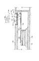
[0071]一実施形態では、前クリーニングチャンバ1100は、基板加熱及び冷却の両方を全て単一の処理環境内で使用するプラズマ増強化学エッチングプロセスを遂行して、前処理ステップを遂行することができる。図12は、前クリーニングチャンバ1100の部分断面図である。前クリーニングチャンバ1100は、蓋アッセンブリ1101、温度制御される基板支持部材1102、温度制御されるチャンバ本体1110、及び処理ゾーン1120を含む真空チャンバである。処理ゾーン1120は、蓋アッセンブリ1101と基板支持部材1102との間の領域である。基板支持部材1102は、一般的に、処理中に基板を支持し、その温度を制御するように適応される。蓋アッセンブリ1101は、プロセスガス供給パネル(図示せず)と、処理ゾーン1120の外部にプラズマを発生するためのプラズマ空洞を画成する第1及び第2の電極(素子1130及び1131)とを含む。プロセスガス供給パネル(図示せず)は、ガス源1160に接続され、このガス源は、1つ以上の反応性ガスを、プラズマ空洞へ、更に、第2の電極1131を通して、処理ゾーン1120へ供給する。第2の電極1131は、基板の上に位置付けられ、プラズマ補助型乾式エッチングプロセスが完了した後に基板を加熱するように適応される。
[0071] In one embodiment, the
[0072]図12は、例示的前クリーニングチャンバ1100を示す部分断面図である。一実施形態では、前クリーニングチャンバ1100は、チャンバ本体1110と、蓋アッセンブリ1101と、支持アッセンブリ1140とを備えている。蓋アッセンブリ1101は、チャンバ本体1110の上端に配設され、また、支持アッセンブリ1140は、チャンバ本体1110内に少なくとも部分的に配設される。チャンバ本体1110は、その側壁に形成されたスリットバルブ開口1111を含み、前クリーニングチャンバ1100の内部へアクセスできるようにする。スリットバルブ開口1111は、基板取り扱いロボット(例えば、図2のロボット113)によりチャンバ本体1110の内部へアクセスできるように選択的に開閉される。
[0072] FIG. 12 is a partial cross-sectional view illustrating an
[0073]1つ以上の実施形態では、チャンバ本体1110は、これを通して熱伝達流体を流すために流体チャンネル1112が形成されている。熱伝達流体は、加熱流体又は冷却材でよく、処理及び基板移送中にチャンバ本体1110の温度を制御するのに使用される。チャンバ本体1110の温度は、チャンバ壁におけるガス又は副産物の望ましからぬ凝縮を防止するために重要である。熱伝達流体は、例えば、水、エチレングリコール、又はその混合物を含む。また、熱伝達流体は、窒素ガスを含んでもよい。
[0073] In one or more embodiments, the
[0074]蓋アッセンブリ1101は、一般的に、蓋アッセンブリ1101内に1つ以上の反応性種を含むプラズマを発生して1つ以上の前処理ステップを遂行するために第1の電極1130を備えている。一実施形態では、第1の電極130は、頂部プレート1131に支持され、そこから電気的に分離される。一実施形態では、第1の電極1130は、電源1132に結合され、一方、第2の電極1131は、接地点に接続される。従って、プロセスガスがガス源1160から頂部プレートに形成されたホール1133を通して処理ゾーン1120へ配送されるときに、第1の電極1130と第2の電極1131との間の容積部に1つ以上のプロセスガスを含むプラズマが発生される。
[0074] The
[0075]ガスを反応性の種へと活性化して反応性種のプラズマを維持することのできる電源1132を使用することができる。例えば、電源1132は、高周波(RF)、直流(DC)又はマイクロ波(MW)電力の形態のエネルギーを処理ゾーン1120へ配送することができる。或いは又、遠隔プラズマジェネレータのような遠隔活性化源を使用して、反応性種のプラズマを発生し、これを前クリーニングチャンバ1100へ配送することもできる。一実施形態では、第2の電極1131は、前クリーニングチャンバ1100内で遂行されるべきプロセスガス及び動作に基づいて加熱されてもよい。一実施形態では、例えば、抵抗ヒータのような加熱素子1135を第2の電極1131又は分配プレートに結合することができる。温度の調整は、第2の電極1131又は分配プレートに結合されたサーモカップルにより容易にすることができる。
[0075] A
[0076]ガス源1160は、典型的に、1つ以上のガスを前クリーニングチャンバ1100へ供給するのに使用される。使用する特定のガス(1つ又は複数)は、前クリーニングチャンバ1100内で遂行されるべきプロセス(1つ又は複数)に依存する。説明上、ガスは、1つ以上の先駆体、還元剤、触媒、担体、パージ、クリーニング、又は任意の混合物、或いはその組合せを含むことができるが、これらに限定されない。典型的に、前クリーニングチャンバ1100に導入される1つ以上のガスは、蓋アッセンブリ1101に流れ込み、次いで、第2の電極1131を通してチャンバ本体1110へ流れ込む。プロセスに基づいて、多数のガスを前クリーニングチャンバ1100へ配送し、前クリーニングチャンバ1100において混合することもできるし、又は前クリーニングチャンバ1100へ配送する前にガスを混合することもできる。チャンバ本体1110に見られるプロセスガスは、次いで、真空アッセンブリ1150により、ライナー1113に形成されたアパーチャー1114及びポンピングチャンネル1115を通して排気される。
[0076] The
[0077]支持アッセンブリ1140は、チャンバ本体1110内に少なくとも部分的に配設することができる。支持アッセンブリ1140は、チャンバ本体1110内で処理するために基板(この図には示さず)を支持する基板支持部材1102を含むことができる。基板支持部材1102は、チャンバ本体1110の底面を貫通して延びるリフトメカニズム(図示せず)に結合することができる。リフトメカニズム(図示せず)は、そのリフトメカニズムの周囲から真空が漏れるのを防止するベローズ(図示せず)によりチャンバ本体1110に柔軟にシールすることができる。リフトメカニズムは、基板支持部材1102をチャンバ本体1110内において処理位置と下部の移送位置との間で垂直に移動させることができる。移送位置は、チャンバ本体1110の側壁に形成されたスリットバルブ開口1111の若干下である。
[0077] The
[0078]1つ以上の実施形態において、基板支持部材1102は、処理されるべき基板を支持するためのフラットな円形表面又は実質的にフラットな円形表面を有する。基板支持部材1102は、アルミニウムで構成されるのが好ましい。基板支持部材1102は、この基板支持部材1102と蓋アッセンブリ1101との間の距離を制御できるようにチャンバ本体1110内を垂直に移動することができる。基板支持部材1102は、リフトピン(図示せず)を受け入れるために貫通形成された1つ以上のボア(図示せず)を含むことができる。各リフトピンは、典型的に、セラミック又はセラミック含有材料で構成され、基板の取扱い及び搬送に使用される。1つ以上の実施形態では、基板(図示せず)は、静電チャック又は真空チャックを使用して基板支持部材1102に固定することができる。1つ以上の実施形態では、基板は、従来のクランプリングのような機械的なクランプ(図示せず)により基板支持部材1102に位置保持することができる。基板は、静電チャックを使用して固定されるのが好ましい。
[0078] In one or more embodiments, the
[0079]支持アッセンブリ1140の温度は、基板支持部材1102の本体に埋め込まれた1つ以上の流体チャンネル1141を通して循環される流体によって制御される。流体チャンネル1141は、基板支持部材1102の基板受け入れ面に均一な熱伝達を与えるために基板支持部材1102の周りに位置付けられるのが好ましい。流体チャンネル1141は、基板支持部材1102を加熱又は冷却するために熱伝達流体を流すことができる。水、窒素、エチレングリコール又はその混合物のような適当な熱伝達流体を使用することができる。支持アッセンブリ1140は、更に、基板支持部材1102の支持面の温度を監視するために埋設サーモカップル(図示せず)を含むことができる。
[0079] The temperature of the
[0080]動作中に、基板支持部材1102は、蓋アッセンブリ1101の至近まで上昇されて、処理中の基板の温度を制御することができる。従って、基板は、加熱素子1135によって加熱される蓋アッセンブリ1101又は分配プレートから放出される放射を経て加熱することができる。或いは又、リフトピンを使用して、基板を基板支持部材1102から、加熱される蓋アッセンブリ1101の至近へ持ち上げることができる。
[0080] During operation, the
[0081]前クリーニングチャンバ内でアンモニア(NH3)及び三フッ化窒素(NF3)混合ガスを使用して基板表面上の自然酸化物を除去するための例示的乾式エッチングプロセスについて以下に説明する。乾式エッチングプロセスは、半導体基板のような基板を前クリーニングチャンバに入れることにより開始される。基板は、処理中に、真空チャック又は静電チャックによって基板支持部材1102の支持アッセンブリ1140に保持されるのが好ましい。チャンバ本体1110は、50℃から80℃、より好ましくは、約65℃の温度に維持されるのが好ましい。チャンバ本体1110のこの温度は、チャンバ本体に配置された流体チャンネル1112に熱伝達媒体を通すことにより維持される。処理中に、基板支持体内に形成された流体チャンネル1112に熱伝達媒体又は冷却材を通すことにより、基板は、65℃未満、例えば、15℃から50℃に冷却される。別の実施形態では、基板は、22℃から40℃の温度に維持される。典型的に、基板支持体は、上述した希望の基板温度に到達するように約22℃未満に維持される。
[0081] An exemplary dry etching process for removing native oxide on a substrate surface using an ammonia (NH 3 ) and nitrogen trifluoride (NF 3 ) gas mixture in a pre-cleaning chamber is described below. . The dry etching process is initiated by placing a substrate, such as a semiconductor substrate, in a preclean chamber. The substrate is preferably held on the
[0082]次いで、アンモニア及び三フッ化窒素ガスが前クリーニングチャンバに導入されて、クリーニング混合ガスを形成する。チャンバに導入される各ガスの量は、可変であり、例えば、除去されるべき酸化物層の厚み、クリーニングされている基板の幾何学的形状、プラズマの体積容量、及びチャンバ本体1110の体積容量を受け入れるように調整することができる。1つの態様において、アンモニア対三フッ化窒素で少なくとも1:1のモル比を有する混合ガスを与えるようにガスが添加される。別の態様では、混合ガスのモル比は、少なくとも約3対1(アンモニア対三フッ化窒素)である。ガスは、5:1(アンモニア対三フッ化窒素)から30:1のモル比で乾式エッチングチャンバに導入されるのが好ましい。混合ガスのモル比は、約5対1(アンモニア対三フッ化窒素)から約10対1であるのが好ましい。また、混合ガスのモル比は、約10:1(アンモニア対三フッ化窒素)から約20:1であってもよい。
[0082] Ammonia and nitrogen trifluoride gas are then introduced into the pre-cleaning chamber to form a cleaning gas mixture. The amount of each gas introduced into the chamber is variable, for example, the thickness of the oxide layer to be removed, the geometry of the substrate being cleaned, the volumetric volume of the plasma, and the volumetric capacity of the
[0083]また、パージガス又は担体ガスが混合ガスに添加されてもよい。例えば、アルゴン、ヘリウム、水素、窒素、又はその混合物のような適当なパージ/担体ガスが使用されてもよい。典型的に、全混合ガスは、約0.05体積%から約20体積%のアンモニア及び三フッ化窒素から作られる。残りは、担体ガスである。一実施形態では、チャンバ本体内の圧力を安定化させるために反応性ガスの前にパージガス又は担体ガスが最初にチャンバ本体1110に導入される。チャンバ本体内の動作圧力は、変化させることができる。典型的に、圧力は、約500ミリトールから約30トールに維持される。好ましくは、圧力は、約1トールから約10トールに維持される。より好ましくは、チャンバ本体内の動作圧力は、約3トールから約6トールに維持される。
[0083] A purge gas or carrier gas may also be added to the mixed gas. For example, a suitable purge / carrier gas such as argon, helium, hydrogen, nitrogen, or mixtures thereof may be used. Typically, the total gas mixture is made from about 0.05% to about 20% by volume ammonia and nitrogen trifluoride. The rest is carrier gas. In one embodiment, a purge gas or carrier gas is first introduced into the
[0084]プラズマ空洞内で混合ガスのプラズマを点火するために約5から約600ワットのRF電力が第1の電極に印加される。RF電力は、100ワット未満であるのが好ましい。電力を印加する周波数は、非常に低く、100kHz未満であるのが更に好ましい。この周波数は、約50kHzから約90kHzの範囲であるのが好ましい。 [0084] About 5 to about 600 watts of RF power is applied to the first electrode to ignite the mixed gas plasma within the plasma cavity. The RF power is preferably less than 100 watts. The frequency at which power is applied is very low, more preferably less than 100 kHz. This frequency is preferably in the range of about 50 kHz to about 90 kHz.
[0085]プラズマエネルギーは、アンモニア及び三フッ化窒素ガスを反応性の種へと解離し、これらの種が結合して、高反応性のフッ化アンモニア(NH4F)化合物及び/又はフッ化水素アンモニウム(NH4F・HF)を気相で形成する。これらの分子は、次いで、第2の電極1131を通して流れ、クリーニングされるべき基板表面と反応する。一実施形態では、担体ガスが最初に前クリーニングチャンバに導入され、担体ガスのプラズマが発生され、次いで、反応性ガス、アンモニア及び三フッ化窒素がプラズマに添加される。
[0085] Plasma energy dissociates ammonia and nitrogen trifluoride gas into reactive species that combine to form highly reactive ammonia fluoride (NH 4 F) compounds and / or fluorides. Ammonium hydrogen (NH 4 F.HF) is formed in the gas phase. These molecules then flow through the
[0086]理論によって縛ろうとは思わないが、エッチングガス、NH4F及び/又はNH4F・HFが自然酸化物表面と反応して、ケイフッ化アンモニウム(NH4)2SiF6、NH3、及びH2O生成物を形成すると考えられる。NH3及びH2Oは、処理条件における蒸気であって、チャンバから、チャンバに取り付けられた真空ポンプにより除去される。基板表面の後ろに(NH4)2SiF6の薄膜が残される。 [0086] While not wishing to be bound by theory, the etching gas, NH 4 F and / or NH 4 F.HF reacts with the native oxide surface to produce ammonium silicofluoride (NH 4 ) 2 SiF 6 , NH 3 , And H 2 O product. NH 3 and H 2 O are vapors at process conditions and are removed from the chamber by a vacuum pump attached to the chamber. A thin film of (NH 4 ) 2 SiF 6 is left behind the substrate surface.
[0087]プラズマ処理ステップを遂行した後に、(NH4)2SiF6の薄膜が基板表面に形成され、基板支持体が、加熱された第2電極の付近のアニール位置へ上昇される。第2電極1131から放射される熱は、(NH4)2SiF6の薄膜を揮発性のSiF4、NH3及びHF生成物へと解離又は昇華させるに充分でなければならない。これらの揮発性生成物は、次いで、チャンバから真空アッセンブリ1150によって除去される。典型的に、基板から薄膜を効果的に昇華させ除去するために、75℃以上の温度が使用される。好ましくは、100℃以上、例えば、約115℃から約200℃の温度が使用される。
[0087] After performing the plasma treatment step, a thin film of (NH 4 ) 2 SiF 6 is formed on the substrate surface, and the substrate support is raised to an anneal position near the heated second electrode. The heat emitted from the
[0088](NH4)2SiF6の薄膜をその揮発性成分へと解離する熱エネルギーは、第2電極によって対流又は放射される。加熱素子1135は、第2電極1131に直結され、第2電極及びそれに熱接触するコンポーネントを約75℃から250℃の温度に加熱するように作動される。1つの態様では、第2電極は、100℃から150℃、例えば、約120℃の温度に加熱される。
[0088] The thermal energy that dissociates the thin film of (NH 4 ) 2 SiF 6 into its volatile components is convected or radiated by the second electrode. The
[0089]基板から膜が除去されると、チャンバがパージされ排気される。次いで、基板を移送位置へ下げ、基板をチャック解除し、スリットバルブ開口1111を通して基板を移送することにより、クリーニングされた基板をチャンバから取り出す。
[0089] Once the film is removed from the substrate, the chamber is purged and evacuated. The substrate is then lowered to the transfer position, the substrate is unchucked, and the substrate is transferred through the
[0090]図13に示すように、準備/分析ステップ302Bを遂行した後に、酸化物エッチング、金属エッチング、EPI、RTP、DPN、PVD、CVD(例えば、CVDポリシリコン、TEOS、等)、又は他の適当な半導体基板処理ステップを含むプロセスのグループの1つから選択される1つ以上の基板処理ステップを使用して処理することができる。
[0090] As shown in FIG. 13, after performing the preparation /
湿式クリーニング型前クリーニングチャンバの構成
[0091]別の実施形態では、露出した基板表面に見られる自然酸化物層及び他の汚染物は、処理シーケンスにおける1つ以上の基板装置製造プロセスステップを遂行する前に、湿式クリーニング型前クリーニングプロセス、以下、湿式クリーニングプロセスという、を使用して除去される。図14は、1つ以上の湿式クリーニング型前クリーニングプロセスステップを遂行することにより装置の歩留り及びプロセスの再現性を改善するのに使用できるプロセスシーケンス301Bを示す。
Structure of wet cleaning type pre-cleaning chamber
[0091] In another embodiment, native oxide layers and other contaminants found on the exposed substrate surface may be pre-cleaned before performing one or more substrate device manufacturing process steps in the processing sequence. It is removed using a process, hereinafter referred to as a wet cleaning process. FIG. 14 illustrates a
[0092]湿式クリーニングプロセス処置は、図13及び図14を参照して説明するように、自然酸化物層、粒子及び他の汚染物を除去するように、基板の表面上で遂行することができる。図14は、例示的プロセスシーケンス301Bを示し、これは、図15に示すクラスターツール101において遂行することができる。図14は、図13に示すプロセスシーケンス301Aと同様であるが、準備/分析ステップ302Aを遂行する前に、準備/分析ステップ302Cが遂行される。一実施形態では、準備/分析ステップ302Aは、基板の準備/分析ステップ(例えば、図5の準備/分析ステップ302)、又は上述した粒子除去ステップを含む。一実施形態では、準備/分析ステップ302Cは、以下に述べる湿式クリーニング型基板準備ステップである。プロセスシーケンス301Bの一実施形態では、準備/分析ステップ302Cを遂行した後に、基板は、基板処理ステップ304及び基板処理ステップ306へ進み、これらステップは、酸化物エッチング、金属エッチング、EPI、RTP、DPN、PVD、CVD(例えば、BLOk、CVDポリシリコン、TEOS、等)、又は他の適当な半導体基板処理ステップを含む半導体装置形成プロセスのグループの1つから選択することができる。
[0092] A wet cleaning process procedure can be performed on the surface of the substrate to remove native oxide layers, particles and other contaminants, as described with reference to FIGS. . FIG. 14 shows an
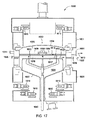
[0093]図15は、処理領域120、リンクモジュール350、及びフロントエンド環境104を含むクラスターツール101の一実施形態を示す平面図である。処理領域120は、一般的に、図2を参照して上述したコンポーネントを備え、これらは、一般的に、1つ以上の処理チャンバ201−204、1つ以上の支援チャンバ211(2つが示されている)、移送チャンバ110、及びロードロックチャンバ106A−Bを含む。ロードロックチャンバ106A−Bは、移送チャンバ110及びリンクモジュール350と連通する。支援チャンバ211は、クラスターツールの他のエリア、例えば、位置114A−F、位置214A−D、及びリンクモジュール350の位置354A−Bに位置付けられてもよいことに注意されたい。
[0093] FIG. 15 is a plan view illustrating one embodiment of a
[0094]リンクモジュール350は、一般的に、フロントエンド環境104を処理領域120に接続する移送領域351を有する。リンクモジュール350は、一般的に、リンクロボット330、及び1つ以上の湿式クリーニングチャンバ360を含む。一実施形態では、リンクロボット330は、このリンクロボット330が、ロードロックチャンバ106A−106Bと、湿式クリーニングチャンバ360と、フロントエンド環境104内の支持ステージ104Aとの間で基板を移送できるように適応されるスライドアッセンブリ331を有する。リンクモジュール350の移送領域351に配設されたリンクロボット330は、一般に、ロードロックチャンバ106と、フロントエンド環境104に装着され位置付けられた支持ステージ104Aとの間で基板を往復させるように直線、回転及び垂直移動することができる。フロントエンド環境104は、一般的に、複数のポッド105に着座されたカセット(図示せず)から大気圧のきれいな環境/エンクロージャーを通して支持ステージ104Aのような何らかの望ましい場所へ基板を移送するのに使用される。
[0094] The
[0095]湿式クリーニングチャンバ360は、一般的に、露出した基板表面上に見られる自然酸化物層及び他の汚染物を、1つ以上の湿式化学的処理ステップを使用して除去するように適応されるチャンバである。湿式クリーニングチャンバ360は、アプライドマテリアルズ社から入手できるEmersionTMチャンバ又はTEMPESTTM湿式クリーニングチャンバでよい。例示的な湿式クリーニングチャンバ360は、例えば、2001年6月25日に出願された共通に譲渡された米国特許出願第09/891,849号、及び2002年4月11日に出願された共通に譲渡された米国特許出願第10/121,635号に更に説明されており、これらは、両方とも参考としてここに全体を援用する。
[0095] The
[0096]処理中に、湿式クリーニングチャンバ360は、一般的に、基板の表面をクリーニングするように構成される。1つの態様において、湿式クリーニングチャンバは、基板の表面上に露出した化合物を機能的グループにおいて終了させる1つ以上のプロセスステップを遂行するように適応される。基板の表面に付着及び/又は形成された機能的グループは、ヒドロキシル(OH)、アルコキシ(OR、但し、R=Me、Et、Pr又はBu)、ハロキシル(OX、但し、X=F、Cl、Br又はI)、ハライド(F、Cl、Br又はI)、酸素基及びアミノ(NR又はNR2、但し、R=H、Me、Et、Pr又はBu)を含む。湿式クリーニングプロセスは、NH3、B2H6、SiH4、SiH6、H2O、HF、HCl、O2、O3、H2O、H2O2、H2、原子H、原子N、原子O、アルコール、アミン、そのプラズマ、その派生物、又はその組合せのような試薬に基板の表面を露出させることができる。これら機能的グループは、基板の表面に付着させるために、その後のCVD又は原子層堆積(ALD)ステップに使用される到来する化学的先駆体のベースとなり得る。一実施形態では、湿式クリーニングプロセスは、基板の表面を約1秒から約2分の期間中、試薬に露出させることができる。また、湿式クリーニングプロセスは、RCA溶液(SC1/SC2)、HFラスト溶液、WVG又はISSGシステムからの水蒸気、過酸化物溶液、酸性溶液、塩基性溶液、そのプラズマ、その派生物又はその組合せに基板の表面を露出させることを含んでもよい。有用な湿式クリーニングプロセスは、共通に譲渡された米国特許第6,858,547号、及び2002年11月21日に出願された“SurfacePre-Treatment for Enhancement of Nucleation of High Dielectric ConstantMaterials”と題する出願中の米国特許出願第10/302,752号(US20030232501号として公告されている)に説明されており、これらは、両方とも参考としてここに全体を援用する。
[0096] During processing, the
[0097]湿式クリーニングプロセスの一実施例では、約10Å以下、例えば、約5Åから約7Åの厚みのを有する化学的酸化物層を形成する第2のプロセスステップに基板を露出させる前に自然酸化物層が除去される。自然酸化物は、HFラスト溶液により除去することができる。湿式クリーニングプロセスは、アプライドマテリアルズ社から入手できるTEMPESTTM湿式クリーニングシステムにおいて遂行することができる。別の実施例では、基板は、WVGシステムから導出される水蒸気に約15秒間露出される。従来のHFラスト処理ステップは、典型的に約1%未満のHFを含む水溶液を処理シーケンスにおけるラストステップとして使用して、露出したシリコン表面上に不動態層を形成する。HFラストプロセスは、高品質のゲート酸化物層を確実に形成するのに有用であろう。 [0097] In one embodiment of the wet cleaning process, native oxidation prior to exposing the substrate to a second process step that forms a chemical oxide layer having a thickness of about 10 mm or less, eg, about 5 mm to about 7 mm. The material layer is removed. The natural oxide can be removed with an HF last solution. The wet cleaning process can be performed in a TEMPEST ™ wet cleaning system available from Applied Materials. In another example, the substrate is exposed to water vapor derived from the WVG system for about 15 seconds. Conventional HF last treatment steps typically use an aqueous solution containing less than about 1% HF as the last step in the treatment sequence to form a passivation layer on the exposed silicon surface. The HF last process will be useful to ensure the formation of a high quality gate oxide layer.
[0098]図14に示すように、準備/分析ステップ302Aを遂行した後に、酸化物エッチング、金属エッチング、EPI、RTP、DPN、PVD、CVD(例えば、CVDポリシリコン、TEOS、等)、又は他の適当な半導体基板処理ステップを含むプロセスのグループの1つから選択された1つ以上の基板処理ステップを使用して基板を処理することができる。
[0098] As shown in FIG. 14, after performing the preparation /
UVクリーニングプロセスを使用するプロセス増強
[0099]半導体装置のサイズが、例えば、45nmノード又はそれ以下というように縮小するにつれて、自然酸化物の成長及び/又は有機汚染物への露出により生じるキュータイムの影響が、より大きな問題となる。形成された半導体装置に対する自然酸化物の成長又は汚染の有害な影響を減少するために、堆積ステップを遂行する前に1つ以上のクリーニングプロセスを遂行して、基板の表面が希望の清潔さレベルとなるよう保証することができる。クラスターツールの一実施形態では、1つ以上の処理チャンバ201−204又は支援チャンバ211は、1つ以上の波長のUV光を配送して基板の表面をクリーニングするように適応される放射源を含み、キュータイムの影響を減少し、ひいては、CVD、PVD又はALD型プロセスのようなその後の堆積プロセスに対して基板を準備する。この構成では、クラスターツール内で基板に対して遂行される処理ステップのシーケンスは、UVエネルギー源を使用して基板表面をクリーニングするステップ(以下、UVクリーニングプロセスという)を含む。堆積ステップの前にUVクリーニングプロセスを追加することは、エピタキシャル(EPI)層堆積ステップの直前にそれを遂行するときには特に有用である。というのは、堆積されるEPI層の核生成、及び形成されるEPI層の応力が、プロセスの開始における表面の状態に非常に敏感だからである。一実施形態では、基板処理シーケンスは、基板の表面の清潔さを向上させると共に、EPI、CVD、PVD又はALD堆積プロセスのような基板製造ステップを遂行する直前に基板表面の状態を繰り返し制御できるように、準備ステップ、例えば、湿式クリーニング型基板準備ステップ(図14の準備/分析ステップ302C)、又は前クリーニング処理ステップ(図13の準備/分析ステップ302B)、及びUVクリーニングプロセスステップを含む。従って、湿式クリーニング型基板準備ステップ又は前クリーニング処理ステップのような準備ステップは、基板表面上の大きな汚染物又は自然酸化物層を除去するのに使用できる一方、UVクリーニングプロセスは、その後の基板処理ステップを実行する直前に基板表面を最終的に準備及び/又は不動態化するのに使用される。
Process enhancement using UV cleaning process
[0099] As the size of semiconductor devices shrinks, for example, 45 nm node or less, the effect of cue time caused by native oxide growth and / or exposure to organic contaminants becomes a greater problem. . In order to reduce the detrimental effects of native oxide growth or contamination on the formed semiconductor device, one or more cleaning processes are performed prior to performing the deposition step so that the surface of the substrate is at a desired clean level. Can be guaranteed. In one embodiment of the cluster tool, one or more processing chambers 201-204 or
[00100]一実施形態において、UVクリーニングプロセスは、クリーニング及び/又は不動態化プロセスを実行する温度を、他の従来のクリーニング技術に対して減少させて、熱履歴の問題を緩和するように使用される。例えば、望ましい量のUV放射を使用するときの処理中の基板温度は、750℃未満でよく、典型的に、700℃未満でよい。1つの態様では、約500℃から約700℃の範囲の温度においてUV増強プロセスが遂行される。EPI堆積ステップの直前に通常使用される従来のシリコン含有基板クリーニング及び不動態化ステップは、典型的に、約750℃から約1000℃の範囲の温度で遂行される。1つの態様において、UV放射の存在中に水素を含む周囲環境において基板を処理することにより、クリーニング及び不動態化プロセスを実行する温度、又は表面をクリーニングするのに必要な時間、或いはその両方の組合せを減少することができる。一実施形態では、UVクリーニングプロセスは、エピタキシャル成長されるシリコン含有膜を堆積するために、きれいで且つ不動態化されたシリコン含有基板表面を準備するように遂行される。 [00100] In one embodiment, the UV cleaning process is used to reduce the temperature at which the cleaning and / or passivation process is performed relative to other conventional cleaning techniques to alleviate thermal history problems. Is done. For example, the substrate temperature during processing when using the desired amount of UV radiation may be less than 750 ° C. and typically less than 700 ° C. In one embodiment, the UV enhancement process is performed at a temperature in the range of about 500 ° C to about 700 ° C. Conventional silicon-containing substrate cleaning and passivation steps commonly used immediately prior to the EPI deposition step are typically performed at temperatures ranging from about 750 ° C to about 1000 ° C. In one embodiment, the temperature of performing the cleaning and passivation process, or the time required to clean the surface, or both, by treating the substrate in an ambient environment containing hydrogen in the presence of UV radiation. Combinations can be reduced. In one embodiment, the UV cleaning process is performed to prepare a clean and passivated silicon-containing substrate surface to deposit an epitaxially grown silicon-containing film.
[00101]図6を参照すれば、一実施形態において、粒子減少チャンバ700は、更に、基板の表面上でクリーニングプロセスを遂行するように適応される。1つの態様において、粒子減少チャンバ700は、エンクロージャー701と、放射源711と、基板支持体704と、加熱素子722と、真空ポンプ736と、水素のような還元ガスを含むクリーニングガスを処理領域710に配送するように適応されるガス配送源735とを備えている。動作に際し、真空ポンプ736は、処理領域710の圧力を基板表面クリーニング及び不動態化プロセス中に約0.1から約80トールに制御するように使用される。加熱素子722及びシステムコントローラ102は、処理中の基板温度を約550℃から約750℃の範囲、典型的に、約550℃から約700℃の範囲に制御するように使用される。システムコントローラ102及び放射源711は、約120nmから約430nmの1つ以上の波長においてUV放射の電力密度を約1mW/cm2から約25mW/cm2の範囲に制御するように使用される。
[00101] Referring to FIG. 6, in one embodiment, the
[00102]一実施例では、UVクリーニングプロセスは、水素を含むクリーニングガスに基板を露出させると同時に、約180nm以下の波長の放射に露出させることにより実行される。UVクリーニングプロセス中に、水素の流量は、約25slmから約50slmの範囲に維持され、一方、基板表面の温度は、約1分から約5分の範囲の時間周期中に、500℃から650℃の範囲にされる。処理領域の圧力は、約0.1トールから約100トールの範囲でよく、典型的に、圧力は、約5トールから約30トールの範囲である。基板の表面へ配送されるUV放射の電力密度は、約2mW/cm2から約25mW/cm2の範囲でよい。 [00102] In one embodiment, the UV cleaning process is performed by exposing the substrate to a cleaning gas comprising hydrogen and simultaneously exposing to radiation having a wavelength of about 180 nm or less. During the UV cleaning process, the hydrogen flow rate is maintained in the range of about 25 slm to about 50 slm, while the substrate surface temperature is between 500 ° C. and 650 ° C. during a time period in the range of about 1 minute to about 5 minutes. Be in range. The pressure in the treatment zone can range from about 0.1 Torr to about 100 Torr, and typically the pressure ranges from about 5 Torr to about 30 Torr. The power density of the UV radiation delivered to the surface of the substrate can range from about 2 mW / cm 2 to about 25 mW / cm 2 .
[00103]一実施形態において、図16に示すように、前クリーニングプロセスステップ302Bを遂行した後であって、プロセスステップ304を遂行する前に、UVクリーニングプロセス302Dが遂行される。図16に示すプロセスシーケンス301Cは、図13に示すプロセスシーケンスと同様であるが、UVクリーニングプロセス302Dを遂行するために、移送ステップA2’及びUVクリーニングプロセス302Dが追加されている。図16は、処理シーケンス内でUVクリーニングプロセスを遂行できる順序を限定することを意図していない点に注意されたい。というのは、クリーニングプロセスは、本発明の範囲から逸脱せずに、いずれの処理ステップの前又は後にも遂行できるからである。一般的に、UVクリーニングプロセス302Dを遂行した後に基板を真空又は不活性環境へ移送し又はそこに維持し、基板表面と酸素又は他の汚染物との相互作用を防止又は最小にして、次の基板処理ステップを遂行する前に、クリーニングされた表面への自然酸化物成長又はダメージを防止することが望まれる。それ故、一般的に、低い分圧の酸素又は他の汚染物を有するクラスターツール内でUVクリーニングプロセスを遂行するのが望ましい。
[00103] In one embodiment, as shown in FIG. 16, a
[00104]別の実施形態では、UV放射源、基板ヒータ及びクリーニングガス源が、クラスターツール内に装着された1つ以上の処理チャンバ(例えば、処理チャンバ201−204)に取り付けられるか又はそこに収容され、UVクリーニングプロセスを実行することができる。この構成では、UVクリーニングプロセスは、堆積プロセスを遂行する前にプロセスチャンバで遂行することができ、従って、個別の移送ステップA3’(図16)は必要とされない。一実施形態では、基板表面に対して遂行される前クリーニングプロセスの処理結果を改善するために、図12に示す前クリーニングチャンバ1100にUV放射源(図示せず)が追加される。
[00104] In another embodiment, the UV radiation source, substrate heater, and cleaning gas source are attached to or in one or more processing chambers (eg, processing chambers 201-204) mounted in the cluster tool. It is housed and a UV cleaning process can be performed. In this configuration, the UV cleaning process can be performed in the process chamber prior to performing the deposition process, so a separate transfer step A3 '(FIG. 16) is not required. In one embodiment, a UV radiation source (not shown) is added to the
[00105]一実施形態では、UVクリーニングプロセスを遂行した後に基板において1つ以上の計測ステップ(例えば、図13−14の準備/分析ステップ302A)を行って、基板の種々の領域の状態を分析し、システムコントローラによって修正アクションを取って、その基板に対するUVクリーニングプロセスの有効性を改善し、及び/又は1つ以上のその後のプロセスで得られる処理結果を改善することができる。一般的に、UVクリーニングプロセス変数は、UVクリーニングプロセス時間、基板表面に供給されるUV電力の強度、及び/又は基板の温度を含むことができる。
[00105] In one embodiment, after performing the UV cleaning process, one or more metrology steps are performed on the substrate (eg, preparation /
[00105]別の実施形態では、UVクリーニングプロセスが遂行された後に、1つ以上の計測ステップ(例えば、図13−14の準備/分析ステップ302A)が遂行されると共に、1つ以上のその後の基板処理ステップ(例えば、PVD、CVD、又はALD堆積ステップ)が基板表面において遂行される。この場合には、計測ステップを使用して、基板表面上の領域の状態を素早く分析し、システムコントローラが、処理シーケンス内の1つ以上のプロセスステップ内の1つ以上のプロセス変数に対して調整を行って、得られる処理結果を改善できるようにする。一般的に、プロセス変数は、UVクリーニングプロセス変数(例えば、クリーニングプロセス時間、UV源の電力)、又は基板処理プロセス変数(例えば、RF電力、プロセス圧力、ガス流量、膜厚み、堆積率、基板温度)のいずれかを含むことができる。一実施例では、XRD装置を使用して、第1基板の表面に堆積された膜の応力を測定し、フィードバックする。それ故、測定された応力が希望の範囲から外れる場合には、システムコントローラは、例えば、基板表面の清潔さを改善し、第2基板に形成される堆積層の応力を減少するようにUVクリーニングプロセスの長さを調整することができる。このプロセスは、エピタキシャル堆積されるシリコン層のように、堆積膜の特性(例えば、応力/歪)が、堆積前の基板表面の状態に非常に敏感である場合に使用するときに重要となる。
[00105] In another embodiment, after the UV cleaning process is performed, one or more metrology steps (eg, preparation /
[00107]クラスターツールに計測ステップを一体化することで、プロセスシーケンスにおける1つ以上の処理ステップの後に望ましい又は望ましからぬ処理結果を迅速にフィードバックして、基板の廃棄及び装置の変化を減少する上で助けとすることができる。また、クラスターツール内の一体化された計測ステップは、1つ以上のプロセスステップの適格性を予め決めるためにクラスターツールを通してテストウェハ又はダミーウェハを走らせる時間を浪費する必要性をおそらく除去することにより、クラスターツールの生産性も改善する。また、クラスターツールの制御された真空又は不活性環境領域(例えば、移送領域110)内にあるか又はそれと連通する1つ以上の計測チャンバの使用は、基板の表面と酸素又は他の汚染物との相互作用を防止し及び/又は最小にし、制御された真空又は不活性環境の外部で計測ステップを遂行することを必要とするプロセスシーケンスに対して、より迅速で且つ現実的な計測結果を与える。従って、一般的に、計測チャンバ(1つ又は複数)をクラスターツールに取り付けて、計測チャンバへの及び計測チャンバからの移送プロセスを、低分圧の酸素又は他の汚染物を有する環境内で遂行するようにクラスターツールを構成することが望ましい。 [00107] Integrating metrology steps into a cluster tool allows rapid feedback of desired or undesired processing results after one or more processing steps in a process sequence, reducing substrate disposal and equipment changes You can help with that. Also, the integrated metrology step within the cluster tool probably eliminates the need to waste time running test wafers or dummy wafers through the cluster tool to pre-qualify one or more process steps. It also improves the productivity of cluster tools. Also, the use of one or more metrology chambers in or in communication with the controlled vacuum or inert environment region (eg, transfer region 110) of the cluster tool can cause the substrate surface and oxygen or other contaminants. Provide faster and more realistic measurement results for process sequences that require performing measurement steps outside of a controlled vacuum or inert environment . Thus, typically, the measurement chamber (s) are attached to the cluster tool and the transfer process to and from the measurement chamber is performed in an environment with low partial pressure oxygen or other contaminants. It is desirable to configure the cluster tool to do so.
UV増強堆積プロセス
[00108]一実施形態では、基板処理チャンバは、基板処理ステップ(例えば、図13、14及び16の基板処理ステップ304−306)の間に基板処理温度を下げるように適応されるUV放射源を含む。基板処理温度を下げる必要性は、特徴部サイズが45nm以下に減少されるにつれて益々重要になってきた。処理温度を下げる必要性は、形成される装置の層間の材料の相互拡散性により生じる装置の歩留まりの問題を最小にするか又は回避する必要性によって生み出される。低いプロセス温度は、基板準備ステップ及び基板製造ステップの両方について必要とされる。基板処理温度を下げると、形成される装置の熱履歴を改善し、ひいては、装置の歩留り、及び形成される装置の使用寿命を改善する。従って、装置製造処理シーケンス内に低い処理温度を含む1つ以上のプロセスステップを使用することが望まれる。
UV enhanced deposition process
[00108] In one embodiment, the substrate processing chamber includes a UV radiation source adapted to reduce the substrate processing temperature during a substrate processing step (eg, substrate processing steps 304-306 of FIGS. 13, 14 and 16). Including. The need to lower substrate processing temperatures has become increasingly important as feature sizes are reduced below 45 nm. The need to lower the processing temperature is created by the need to minimize or avoid device yield problems caused by interdiffusion of materials between the layers of the device being formed. Low process temperatures are required for both the substrate preparation step and the substrate manufacturing step. Lowering the substrate processing temperature improves the thermal history of the device formed, and thus improves the device yield and the service life of the device formed. Accordingly, it is desirable to use one or more process steps that include a low process temperature within the device manufacturing process sequence.
[00109]このタスクを達成するために、基板処理チャンバ、以下、処理チャンバという、は、装置製造プロセスを遂行するステップの間に基板の1つ以上の表面をUV放射に露出させる。使用中に、UV放射源は、基板の表面上に堆積又はエッチングプロセスを生じさせる熱エネルギーの必要性を減少させるために、基板の表面に充分なエネルギーを与えるように適応される。一般的に、約5から約25mW/cm2の電力密度において約120から約430ナノメートル(nm)の波長でUV放射を基板の表面に配送するように適応される放射源は、ほとんどの従来のCVD又はALDプロセスを助ける上で有用であると考えられる。UV放射の波長及び配送電力は、所与の温度、先駆体及び基板の組合せに対して調整を必要とすることがある点に注意されたい。放射源からの放射は、キセノン、アルゴン、クリプトン、窒素、塩化キセノン、フッ化クリプトン、フッ化アルゴンのような元素を含むランプによって供給することができる。典型的な放射源は、従来のUVランプ(例えば、水銀蒸気ランプ)又は他の同様の装置でよい。異なる放出波長を有するUV放射源の組合せを使用してもよい。一実施形態では、処理チャンバ内の圧力は、約0.1から約80トールの範囲である。 [00109] To accomplish this task, a substrate processing chamber, hereinafter referred to as a processing chamber, exposes one or more surfaces of the substrate to UV radiation during the steps of performing the device manufacturing process. In use, the UV radiation source is adapted to provide sufficient energy to the surface of the substrate to reduce the need for thermal energy to cause a deposition or etching process on the surface of the substrate. In general, radiation sources adapted to deliver UV radiation to the surface of a substrate at a wavelength of about 120 to about 430 nanometers (nm) at a power density of about 5 to about 25 mW / cm 2 are most conventional. It is considered useful in assisting the CVD or ALD process. Note that the wavelength of UV radiation and the power delivered may need to be adjusted for a given temperature, precursor and substrate combination. Radiation from the radiation source can be provided by a lamp containing elements such as xenon, argon, krypton, nitrogen, xenon chloride, krypton fluoride, argon fluoride. A typical radiation source may be a conventional UV lamp (eg, a mercury vapor lamp) or other similar device. Combinations of UV radiation sources having different emission wavelengths may be used. In one embodiment, the pressure in the processing chamber ranges from about 0.1 to about 80 Torr.
[00110]図16は、図2−図3に示すクラスターツール100の1つ以上の処理チャンバ201−204として使用できる例示的プロセスチャンバ1600の概略側部断面図である。一実施形態では、図16に示すように、堆積プロセスチャンバは、プロセスチャンバ1600の種々の機能的要素を包囲するステンレススチールのハウジング構造体1601を含む。石英チャンバ1630は、UV放射源1608が収容される上部石英チャンバ1605と、処理体積部1618が収容される下部石英チャンバ1624とを含む。処理体積部1618には反応性の種が与えられ、処理体積部1618から処理副産物が取り出される。基板1614がペデスタル1617に載せられ、反応性の種が基板1614の表面1616へ付与され、その後に、表面1616から副産物が除去される。赤外線ランプ1610を使用して、基板1614及び処理体積部1618の加熱が行われる。赤外線ランプ1610からの放射は、上部石英チャンバ1605の上部石英窓1604、及び下部石英チャンバ1624の下部石英部分1603を通して進行する。上部石英チャンバ1605の1つ以上の冷却ガスは、入口1611を経て入り、出口1628を通して出る(1613)。プロセスチャンバがCVD又はALD型プロセスチャンバである一実施形態では、下部石英チャンバ1624に対する先駆体、並びに希釈、パージ及び通気ガスが入口1620を通して入り、出口1638を通して出る(1622)。出口1628及び1638は、同じ真空ポンプに連通しているか、又は個別のポンプを使用して同じ圧力になるよう制御され、上部石英チャンバ1605及び下部石英チャンバ1624の圧力が等しくなるようにする。従って、UV放射は、反応性の種を付勢するのに使用されると共に、基板の表面1616に反応物質を吸着し、そこからプロセス副産物を脱着する上で助けとなる。例示的堆積チャンバと、UVクリーニングプロセスと、UV補助型堆積プロセスを使用してEPI膜を堆積するプロセスとは、参考としてここに全体を援用する2004年6月10日に出願された共通に譲渡された米国特許出願第10/866,471号に更に説明されている。
[00110] FIG. 16 is a schematic side cross-sectional view of an
[00111]一実施例では、プロセスチャンバ1600において、ジシラン(Si2H6)及びアンモニア(NH3)の混合物を好ましくは約400℃の温度で使用する一方、UV放射を、約172nmの範囲内の波長で約5から約10mW/cm2の電力密度において配送して、窒化シリコン(SiN)膜の堆積が実行される。典型的に、従来のSiN堆積プロセスは、約650℃以上の温度を必要とする。
[00111] In one embodiment, in the
[00112]クラスターツールの一実施形態では、1つ以上のUV補助型基板処理ステップ(例えば、堆積ステップ)を遂行した後に、1つ以上の計測ステップ(例えば、図13−14の準備/分析ステップ302A)が遂行される。この場合には、計測ステップを使用して、基板表面上に堆積される1つ以上の層の状態を迅速に分析し、システムコントローラが基板処理ステップのプロセス変数に対して調整を行って、基板表面に層を形成するプロセスを改善できるようにする。一般的に、プロセス変数は、例えば、UV放射強度(例えば、電力)、堆積時間、処理圧力、プロセスガスの流量、RF電力、膜厚み、又は基板温度を含むことができる。一実施例では、XRD装置を使用して、第1基板の表面に堆積される膜の応力を測定し且つフィードバックし、システムコントローラが、例えば、その後の堆積プロセス中にUV電力を調整し、UV補助型堆積プロセスを使用して形成される層における膜特性、例えば、応力を改善できるようにする。このプロセスは、堆積される膜の特性(例えば、応力/歪)が堆積プロセス中に熱環境に非常に敏感である場合に使用したときに重要となる。クラスターツールに計測プロセスステップを一体化することは、1つ以上の基板製造プロセスステップの後に得られる望ましい又は望ましからぬ処理結果を迅速にフィードバックできるようにし、ひいては、誤って処理される基板の数を減少することにより装置の歩留まりを改善すると共に、プロセスシーケンス内で遂行される1つ以上のプロセスの適格性を予め決めるためにクラスターツールで遂行されるプロセスシーケンス内に含まれる1つ以上のプロセスステップを通してテストウェハを走らせる時間を浪費する必要性を除去することにより、クラスターツールの生産性を改善する上で助けとなろう。 [00112] In one embodiment of the cluster tool, after performing one or more UV assisted substrate processing steps (eg, deposition steps), one or more metrology steps (eg, preparation / analysis steps of FIGS. 13-14). 302A) is performed. In this case, the metrology step is used to quickly analyze the state of one or more layers deposited on the substrate surface and the system controller adjusts to the process variables of the substrate processing step to To improve the process of forming layers on the surface. In general, process variables can include, for example, UV radiation intensity (eg, power), deposition time, process pressure, process gas flow rate, RF power, film thickness, or substrate temperature. In one embodiment, an XRD apparatus is used to measure and feedback the stress of the film deposited on the surface of the first substrate, and the system controller adjusts the UV power, for example during a subsequent deposition process, It enables film properties, such as stress, to be improved in layers formed using an assisted deposition process. This process is important when used when the properties of the deposited film (eg, stress / strain) are very sensitive to the thermal environment during the deposition process. Integrating metrology process steps into a cluster tool allows for quick feedback of desired or undesired processing results obtained after one or more substrate manufacturing process steps, and thus for erroneously processed substrates. One or more included in the process sequence performed in the cluster tool to improve device yield by reducing the number and predetermine qualification of one or more processes performed in the process sequence By eliminating the need to waste time running test wafers through process steps, it will help improve the productivity of cluster tools.
[00113]以上、本発明の実施形態を説明したが、本発明の基本的な範囲から逸脱せずに、他の実施形態及び更に別の実施形態を案出することができ、従って、本発明の範囲は、特許請求の範囲によって限定されるものとする。 [00113] While embodiments of the present invention have been described above, other and further embodiments can be devised without departing from the basic scope of the present invention, and thus the present invention. Is intended to be limited by the scope of the claims.
100…クラスターツール、102…システムコントローラ、104…フロントエンド環境、104B…移送領域、106…ロードロックチャンバ、108A−B…ファクトリインターフェイスロボット、110…移送チャンバ、113…ロボット、113A…ブレードアッセンブリ、113B…アームアッセンブリ、113C…ロボット駆動アッセンブリ、114A−114F…処理位置、116A−B…サービスチャンバ、201−204…基板処理チャンバ、211…支援チャンバ、214A−214E…位置、700…粒子減少チャンバ、701…エンクロージャー、702…チャンバ本体、703…チャンバ蓋、704…基板支持体、705…透明領域、706…シール、707…基板支持面、711…放射源、720…リフトアッセンブリ、722…加熱素子、750…計測チャンバ、752…チャンバ本体、753…チャンバ蓋、754…基板支持体、755…透明領域、756…シール、757…基板支持面、761…エンクロージャー、770…処理領域、800、801…支援チャンバアッセンブリ、804…基板支持体、808…支持体、811…測定アッセンブリ、812…センサ、813…放射源、820…リフトアッセンブリ、1100…前クリーニングチャンバ、1101…蓋アッセンブリ、1102…基板支持部材、1110…チャンバ本体、1112…流体チャンネル、1114…アパーチャー、1115…ポンピングチャンネル、1120…処理ゾーン、1160…ガス源、1130…第1電極、1131…第2電極、1132…電源、1140…支持アッセンブリ、1141…流体チャンネル、1150…真空アッセンブリ、1600…プロセスチャンバ、1605…上部石英チャンバ、1608…UV放射源、1610…赤外線ランプ、1614…基板、1616…表面、1618…処理体積部、1624…下部石英チャンバ
DESCRIPTION OF
Claims (35)
上記移送領域内に配設され、基板の表面の特性を測定するように適応される第1の支援チャンバと、
上記移送領域に連通する基板処理チャンバと、
上記基板処理チャンバ内で処理ステップを遂行する前に基板の表面を準備するように適応される前クリーニングチャンバと、
を備えた基板処理装置。 One or more walls forming a transfer area in which the robot is disposed;
A first support chamber disposed within the transfer region and adapted to measure a surface property of the substrate;
A substrate processing chamber in communication with the transfer region;
A pre-cleaning chamber adapted to prepare a surface of the substrate before performing a processing step in the substrate processing chamber;
A substrate processing apparatus comprising:
上記移送領域に連通する1つ以上の基板処理チャンバと、
上記ロボットと移送可能に連通し、基板の表面の特性を測定するように適応される支援チャンバと、
上記移送領域に連通する処理チャンバであって、
この処理チャンバの処理領域内に位置付けられた基板支持体、及び
上記基板支持体に位置付けられた基板の表面に1つ以上のUV波長の光を配送するように適応される第1の放射源、
を含むような前記処理チャンバと、
を備えた基板処理装置。 One or more walls forming a transfer area in which the robot is disposed;
One or more substrate processing chambers in communication with the transfer region;
A support chamber in transportable communication with the robot and adapted to measure a surface property of the substrate;
A processing chamber in communication with the transfer region,
A substrate support positioned within the processing region of the processing chamber, and a first radiation source adapted to deliver light of one or more UV wavelengths to a surface of the substrate positioned on the substrate support;
Said processing chamber comprising:
A substrate processing apparatus comprising:
上記ロボットと連通し、大気圧より低い圧力に排気されるように適応されるロードロックと、
上記ポッドに位置付けられた2つ以上の基板の1つを上記ポッドと上記ロードロックとの間で移送するように適応される第2のロボットと、
を更に備えた請求項7に記載の装置。 A pod adapted to contain two or more substrates;
A load lock that communicates with the robot and is adapted to be exhausted to a pressure below atmospheric pressure;
A second robot adapted to transfer one of the two or more substrates positioned in the pod between the pod and the load lock;
8. The apparatus of claim 7, further comprising:
上記ロボットと移送可能に連通し、基板の表面の特性を測定するように適応される支援チャンバと、
上記移送領域に連通する第1の処理チャンバであって、
この処理チャンバの処理領域内に位置付けられた基板支持体、及び
1つ以上のUV波長の光を、上記基板支持体に位置付けられた基板の表面に配送するように適応される第1の放射源、
を含むような前記第1の処理チャンバと、
上記移送領域に連通する第2の処理チャンバであって、
この処理チャンバの処理領域内に位置付けられた基板支持体、
1つ以上のUV波長の光を、上記基板支持体に位置付けられた基板の表面に配送するように適応される第2の放射源、及び
水素を含むクリーニングガスを上記処理領域へ配送するように適応されるガス源、
を含むような第2の処理チャンバと、
を備えた基板処理装置。 One or more walls forming a transfer area in which the robot is disposed;
A support chamber in transportable communication with the robot and adapted to measure a surface property of the substrate;
A first processing chamber in communication with the transfer region,
A substrate support positioned within the processing region of the processing chamber, and a first radiation source adapted to deliver one or more UV wavelengths of light to a surface of the substrate positioned on the substrate support ,
Said first processing chamber comprising:
A second processing chamber in communication with the transfer region,
A substrate support positioned within the processing region of the processing chamber;
A second radiation source adapted to deliver light of one or more UV wavelengths to a surface of the substrate positioned on the substrate support, and to deliver a cleaning gas comprising hydrogen to the processing region Gas source adapted,
A second processing chamber comprising:
A substrate processing apparatus comprising:
基板処理チャンバ内で基板の表面を変更するステップと、
基板の表面を変更した後に基板の領域の特性を測定するステップと、
上記測定された特性を、システムコントローラに記憶された値と比較するステップと、
基板の表面を変更するプロセスの間に、上記測定された特性とシステムコントローラに記憶された値との上記比較に基づいて、プロセス変数を変更するステップと、
を備えた方法。 In a method of forming a semiconductor device in a cluster tool,
Changing the surface of the substrate within the substrate processing chamber;
Measuring the characteristics of the area of the substrate after changing the surface of the substrate;
Comparing the measured characteristic to a value stored in a system controller;
Changing a process variable during the process of changing the surface of the substrate based on the comparison of the measured characteristic and the value stored in the system controller;
With a method.
約120nmから約430nmの範囲内の少なくとも1つの波長を有する放射に基板の表面を露出させる段階と、
水素を含むクリーニングガスを基板の表面に与える段階と、
約750℃より低い温度に基板を加熱する段階と、
を含む請求項23に記載の方法。 Further comprising removing contaminants from the surface of the substrate prior to forming the device features, and removing the contaminants comprises:
Exposing the surface of the substrate to radiation having at least one wavelength in the range of about 120 nm to about 430 nm;
Applying a cleaning gas containing hydrogen to the surface of the substrate;
Heating the substrate to a temperature below about 750 ° C .;
24. The method of claim 23, comprising:
基板処理チャンバ内で基板の表面を変更するステップと、
上記クラスターツールの移送領域内に配設されたロボットを使用して、その移送領域に基板を位置付けるステップと、
上記移送領域に位置付けられた基板の表面の特性を測定するステップと、
上記測定された特性を、システムコントローラに記憶された値と比較するステップと、
基板の表面を変更するプロセスにおいて、上記測定された特性とシステムコントローラに記憶された値との上記比較に基づいて、プロセス変数を変更するステップと、
を備えた方法。 In a method of forming a semiconductor device in a cluster tool,
Changing the surface of the substrate within the substrate processing chamber;
Using a robot disposed in the transfer area of the cluster tool to position the substrate in the transfer area;
Measuring the characteristics of the surface of the substrate positioned in the transfer region;
Comparing the measured characteristic to a value stored in a system controller;
Changing a process variable based on the comparison of the measured characteristic and a value stored in a system controller in a process of changing the surface of the substrate;
With a method.
約120nmから約430nmの範囲内の少なくとも1つの波長を有する放射に基板の表面を露出させる段階と、
水素を含むクリーニングガスを基板の表面に与える段階と、
約750℃より低い温度に基板を加熱する段階と、
を含む請求項29に記載の方法。 Further comprising removing contaminants from the surface of the substrate prior to forming the device features, and removing the contaminants comprises:
Exposing the surface of the substrate to radiation having at least one wavelength in the range of about 120 nm to about 430 nm;
Applying a cleaning gas containing hydrogen to the surface of the substrate;
Heating the substrate to a temperature below about 750 ° C .;
30. The method of claim 29, comprising:
The step of modifying the surface of the substrate further comprises exposing the surface of the substrate to radiation having at least one wavelength in the range of about 120 nm to about 430 nm during the processing step of modifying the surface. 30. The method according to 29.
Applications Claiming Priority (3)
| Application Number | Priority Date | Filing Date | Title |
|---|---|---|---|
| US80651806P | 2006-07-03 | 2006-07-03 | |
| US11/460,864 US20070134821A1 (en) | 2004-11-22 | 2006-07-28 | Cluster tool for advanced front-end processing |
| PCT/US2007/072264 WO2008005773A2 (en) | 2006-07-03 | 2007-06-27 | Cluster tool for advanced front-end processing |
Publications (2)
| Publication Number | Publication Date |
|---|---|
| JP2009543355A true JP2009543355A (en) | 2009-12-03 |
| JP2009543355A5 JP2009543355A5 (en) | 2010-08-05 |
Family
ID=38895329
Family Applications (1)
| Application Number | Title | Priority Date | Filing Date |
|---|---|---|---|
| JP2009518542A Pending JP2009543355A (en) | 2006-07-03 | 2007-06-27 | Cluster tools for advanced front-end processing |
Country Status (5)
| Country | Link |
|---|---|
| EP (1) | EP2041774A2 (en) |
| JP (1) | JP2009543355A (en) |
| KR (1) | KR20090035578A (en) |
| TW (1) | TW200811916A (en) |
| WO (1) | WO2008005773A2 (en) |
Cited By (13)
| Publication number | Priority date | Publication date | Assignee | Title |
|---|---|---|---|---|
| JP2013514673A (en) * | 2009-12-17 | 2013-04-25 | アプライド マテリアルズ インコーポレイテッド | Method for forming NMOS epilayer |
| JP2013543651A (en) * | 2010-09-14 | 2013-12-05 | アプライド マテリアルズ インコーポレイテッド | Transfer chamber metering to improve device yield |
| JP2016072625A (en) * | 2014-09-30 | 2016-05-09 | ラム リサーチ コーポレーションLam Research Corporation | Method and apparatus for rf compensation in plasma assisted atomic layer deposition |
| KR20160126914A (en) * | 2015-04-23 | 2016-11-02 | 어플라이드 머티어리얼스, 인코포레이티드 | External substrate rotation in a semiconductor processing system |
| JP2018527456A (en) * | 2015-06-19 | 2018-09-20 | アプライド マテリアルズ インコーポレイテッドApplied Materials,Incorporated | PVD deposition and annealing of multilayer metal dielectric films |
| JP2019501518A (en) * | 2015-11-13 | 2019-01-17 | アプライド マテリアルズ インコーポレイテッドApplied Materials, Inc. | Semiconductor device processing method and semiconductor device processing system and apparatus |
| US10697059B2 (en) | 2017-09-15 | 2020-06-30 | Lam Research Corporation | Thickness compensation by modulation of number of deposition cycles as a function of chamber accumulation for wafer to wafer film thickness matching |
| JP2020123675A (en) * | 2019-01-30 | 2020-08-13 | 日立金属株式会社 | Semiconductor manufacturing apparatus management system and method therefor |
| KR20200124315A (en) * | 2018-03-20 | 2020-11-02 | 도쿄엘렉트론가부시키가이샤 | Self-recognition and correction heterogeneous platform including integrated semiconductor process module, and method for using the same |
| JP2021518673A (en) * | 2018-03-20 | 2021-08-02 | 東京エレクトロン株式会社 | Board processing tools and usage with integrated measurement |
| JP2021518674A (en) * | 2018-03-20 | 2021-08-02 | 東京エレクトロン株式会社 | Self-awareness and correction heterogeneous platforms incorporating integrated semiconductor processing modules and how to use them |
| JP2021168422A (en) * | 2017-09-20 | 2021-10-21 | 株式会社Kokusai Electric | Substrate-processing machine, semiconductor device-manufacturing method and program |
| US20220102193A1 (en) * | 2020-09-25 | 2022-03-31 | SK Hynix Inc. | Semiconductor device and method for fabricating the same |
Families Citing this family (25)
| Publication number | Priority date | Publication date | Assignee | Title |
|---|---|---|---|---|
| US8022372B2 (en) | 2008-02-15 | 2011-09-20 | Veeco Instruments Inc. | Apparatus and method for batch non-contact material characterization |
| US7838431B2 (en) * | 2008-06-14 | 2010-11-23 | Applied Materials, Inc. | Method for surface treatment of semiconductor substrates |
| US7964858B2 (en) | 2008-10-21 | 2011-06-21 | Applied Materials, Inc. | Ultraviolet reflector with coolant gas holes and method |
| KR20120042919A (en) * | 2009-08-13 | 2012-05-03 | 김남진 | Apparatus for forming layer |
| TWI525744B (en) | 2011-05-31 | 2016-03-11 | 維克儀器公司 | Heated wafer carrier profiling |
| KR102168043B1 (en) * | 2012-07-02 | 2020-10-20 | 어플라이드 머티어리얼스, 인코포레이티드 | Aluminum-nitride buffer and active layers by physical vapor deposition |
| WO2014025918A1 (en) * | 2012-08-08 | 2014-02-13 | Applied Materials, Inc | Linked vacuum processing tools and methods of using the same |
| KR101463984B1 (en) * | 2013-02-15 | 2014-11-26 | 최대규 | Plasma process system |
| US9627608B2 (en) * | 2014-09-11 | 2017-04-18 | Lam Research Corporation | Dielectric repair for emerging memory devices |
| US20160240405A1 (en) * | 2015-02-12 | 2016-08-18 | Applied Materials, Inc. | Stand alone anneal system for semiconductor wafers |
| WO2017073396A1 (en) * | 2015-10-28 | 2017-05-04 | 東京エレクトロン株式会社 | Substrate processing method, substrate processing apparatus, substrate processing system and storage medium |
| KR20190041030A (en) | 2016-09-15 | 2019-04-19 | 어플라이드 머티어리얼스, 인코포레이티드 | Integrated system for semiconductor process |
| TWI700750B (en) * | 2017-01-24 | 2020-08-01 | 美商應用材料股份有限公司 | Method and apparatus for selective deposition of dielectric films |
| JP7158133B2 (en) * | 2017-03-03 | 2022-10-21 | アプライド マテリアルズ インコーポレイテッド | Atmosphere-controlled transfer module and processing system |
| CN109154077A (en) * | 2017-04-28 | 2019-01-04 | 应用材料公司 | For clean the vacuum system used in manufacture OLED device method, on substrate vacuum deposition come manufacture OLED device method and on substrate vacuum deposition come the equipment that manufactures OLED device |
| KR20200142601A (en) * | 2018-05-16 | 2020-12-22 | 어플라이드 머티어리얼스, 인코포레이티드 | Atomic layer self-aligned substrate processing and integrated toolset |
| US20190362989A1 (en) * | 2018-05-25 | 2019-11-28 | Applied Materials, Inc. | Substrate manufacturing apparatus and methods with factory interface chamber heating |
| CN111507076B (en) * | 2019-01-29 | 2022-07-05 | 北京新唐思创教育科技有限公司 | Common case courseware making method and device for teaching system and terminal |
| WO2022186775A1 (en) * | 2021-03-02 | 2022-09-09 | Agency For Science, Technology And Research | A preparation chamber for cleaning and repair sapphire surface for the epitaxial growth of compound materials |
| US20230032146A1 (en) * | 2021-07-27 | 2023-02-02 | Applied Materials, Inc. | Simultaneous in process metrology for cluster tool architecture |
| KR102424853B1 (en) * | 2021-10-12 | 2022-07-25 | 주식회사 바코솔루션 | Apparatus for processing semiconductor substrate |
| KR102418530B1 (en) * | 2021-10-12 | 2022-07-07 | 주식회사 바코솔루션 | Apparatus for processing semiconductor substrate |
| KR102418534B1 (en) * | 2021-10-12 | 2022-07-07 | 주식회사 바코솔루션 | Cluster tool for processing semiconductor substrate and method for controlling the same |
| CN114000192B (en) * | 2021-10-29 | 2023-10-13 | 北京北方华创微电子装备有限公司 | Semiconductor process equipment and method for monitoring wafer position state |
| CN114904822B (en) * | 2022-03-31 | 2023-09-26 | 上海果纳半导体技术有限公司 | Manipulator cleaning device, cleaning method and semiconductor device |
Citations (7)
| Publication number | Priority date | Publication date | Assignee | Title |
|---|---|---|---|---|
| JPH0249428A (en) * | 1988-05-12 | 1990-02-19 | Mitsubishi Electric Corp | Method and apparatus for forming thin film on surface of semiconductor substrate |
| JPH05102502A (en) * | 1991-10-09 | 1993-04-23 | Mitsui Toatsu Chem Inc | Amorphous solar cell |
| JPH05275343A (en) * | 1992-03-27 | 1993-10-22 | Toshiba Corp | Substrate treatment apparatus |
| JPH09186108A (en) * | 1995-12-27 | 1997-07-15 | Tokyo Electron Ltd | Clustered tool apparatus |
| JP2002502108A (en) * | 1997-12-08 | 2002-01-22 | クエスター テクノロジー インコーポレイテッド | Surface modification of semiconductors using electromagnetic radiation |
| JP2002270596A (en) * | 2001-03-12 | 2002-09-20 | Matsushita Electric Ind Co Ltd | Apparatus for fabricating semiconductor device |
| JP2003115578A (en) * | 2001-10-05 | 2003-04-18 | Canon Inc | Nonvolatile solid magnetic memory, its manufacturing method and multichip package |
Family Cites Families (2)
| Publication number | Priority date | Publication date | Assignee | Title |
|---|---|---|---|---|
| US6081334A (en) * | 1998-04-17 | 2000-06-27 | Applied Materials, Inc | Endpoint detection for semiconductor processes |
| US7431795B2 (en) * | 2004-07-29 | 2008-10-07 | Applied Materials, Inc. | Cluster tool and method for process integration in manufacture of a gate structure of a field effect transistor |
-
2007
- 2007-06-27 WO PCT/US2007/072264 patent/WO2008005773A2/en active Application Filing
- 2007-06-27 EP EP07812383A patent/EP2041774A2/en not_active Withdrawn
- 2007-06-27 KR KR1020097002228A patent/KR20090035578A/en not_active Application Discontinuation
- 2007-06-27 JP JP2009518542A patent/JP2009543355A/en active Pending
- 2007-07-03 TW TW096124192A patent/TW200811916A/en unknown
Patent Citations (7)
| Publication number | Priority date | Publication date | Assignee | Title |
|---|---|---|---|---|
| JPH0249428A (en) * | 1988-05-12 | 1990-02-19 | Mitsubishi Electric Corp | Method and apparatus for forming thin film on surface of semiconductor substrate |
| JPH05102502A (en) * | 1991-10-09 | 1993-04-23 | Mitsui Toatsu Chem Inc | Amorphous solar cell |
| JPH05275343A (en) * | 1992-03-27 | 1993-10-22 | Toshiba Corp | Substrate treatment apparatus |
| JPH09186108A (en) * | 1995-12-27 | 1997-07-15 | Tokyo Electron Ltd | Clustered tool apparatus |
| JP2002502108A (en) * | 1997-12-08 | 2002-01-22 | クエスター テクノロジー インコーポレイテッド | Surface modification of semiconductors using electromagnetic radiation |
| JP2002270596A (en) * | 2001-03-12 | 2002-09-20 | Matsushita Electric Ind Co Ltd | Apparatus for fabricating semiconductor device |
| JP2003115578A (en) * | 2001-10-05 | 2003-04-18 | Canon Inc | Nonvolatile solid magnetic memory, its manufacturing method and multichip package |
Cited By (30)
| Publication number | Priority date | Publication date | Assignee | Title |
|---|---|---|---|---|
| JP2013514673A (en) * | 2009-12-17 | 2013-04-25 | アプライド マテリアルズ インコーポレイテッド | Method for forming NMOS epilayer |
| JP2013543651A (en) * | 2010-09-14 | 2013-12-05 | アプライド マテリアルズ インコーポレイテッド | Transfer chamber metering to improve device yield |
| US10103288B2 (en) | 2010-09-14 | 2018-10-16 | Applied Materials, Inc. | Transfer chamber metrology for improved device yield |
| JP2016072625A (en) * | 2014-09-30 | 2016-05-09 | ラム リサーチ コーポレーションLam Research Corporation | Method and apparatus for rf compensation in plasma assisted atomic layer deposition |
| KR102543643B1 (en) * | 2015-04-23 | 2023-06-13 | 어플라이드 머티어리얼스, 인코포레이티드 | External substrate rotation in a semiconductor processing system |
| KR20160126914A (en) * | 2015-04-23 | 2016-11-02 | 어플라이드 머티어리얼스, 인코포레이티드 | External substrate rotation in a semiconductor processing system |
| JP2017005242A (en) * | 2015-04-23 | 2017-01-05 | アプライド マテリアルズ インコーポレイテッドApplied Materials,Incorporated | External substrate rotation in semiconductor processing system |
| JP2022023889A (en) * | 2015-04-23 | 2022-02-08 | アプライド マテリアルズ インコーポレイテッド | External substrate rotation in semiconductor processing system |
| US11574825B2 (en) | 2015-04-23 | 2023-02-07 | Applied Materials, Inc. | External substrate system rotation in a semiconductor processing system |
| JP7350035B2 (en) | 2015-04-23 | 2023-09-25 | アプライド マテリアルズ インコーポレイテッド | External substrate rotation in semiconductor processing systems |
| US10879177B2 (en) | 2015-06-19 | 2020-12-29 | Applied Materials, Inc. | PVD deposition and anneal of multi-layer metal-dielectric film |
| JP2018527456A (en) * | 2015-06-19 | 2018-09-20 | アプライド マテリアルズ インコーポレイテッドApplied Materials,Incorporated | PVD deposition and annealing of multilayer metal dielectric films |
| JP2019501518A (en) * | 2015-11-13 | 2019-01-17 | アプライド マテリアルズ インコーポレイテッドApplied Materials, Inc. | Semiconductor device processing method and semiconductor device processing system and apparatus |
| US10697059B2 (en) | 2017-09-15 | 2020-06-30 | Lam Research Corporation | Thickness compensation by modulation of number of deposition cycles as a function of chamber accumulation for wafer to wafer film thickness matching |
| US11286560B2 (en) | 2017-09-15 | 2022-03-29 | Lam Research Corporation | Thickness compensation by modulation of number of deposition cycles as a function of chamber accumulation for wafer to wafer film thickness matching |
| JP7162705B2 (en) | 2017-09-20 | 2022-10-28 | 株式会社Kokusai Electric | SUBSTRATE PROCESSING APPARATUS, SEMICONDUCTOR DEVICE MANUFACTURING METHOD AND PROGRAM |
| JP2021168422A (en) * | 2017-09-20 | 2021-10-21 | 株式会社Kokusai Electric | Substrate-processing machine, semiconductor device-manufacturing method and program |
| JP2021518672A (en) * | 2018-03-20 | 2021-08-02 | 東京エレクトロン株式会社 | Self-awareness and correction heterogeneous platforms incorporating integrated semiconductor processing modules and how to use them |
| JP2021518674A (en) * | 2018-03-20 | 2021-08-02 | 東京エレクトロン株式会社 | Self-awareness and correction heterogeneous platforms incorporating integrated semiconductor processing modules and how to use them |
| JP2021518673A (en) * | 2018-03-20 | 2021-08-02 | 東京エレクトロン株式会社 | Board processing tools and usage with integrated measurement |
| CN112106182A (en) * | 2018-03-20 | 2020-12-18 | 东京毅力科创株式会社 | Self-sensing corrective heterogeneous platform incorporating integrated semiconductor processing modules and methods of use thereof |
| KR20200124315A (en) * | 2018-03-20 | 2020-11-02 | 도쿄엘렉트론가부시키가이샤 | Self-recognition and correction heterogeneous platform including integrated semiconductor process module, and method for using the same |
| JP7295359B2 (en) | 2018-03-20 | 2023-06-21 | 東京エレクトロン株式会社 | Substrate processing tools with integrated metrology and methods of use |
| JP7348440B2 (en) | 2018-03-20 | 2023-09-21 | 東京エレクトロン株式会社 | Self-aware and corrective heterogeneous platform incorporating integrated semiconductor processing module and method of use thereof |
| JP7402399B2 (en) | 2018-03-20 | 2023-12-21 | 東京エレクトロン株式会社 | Self-aware and corrective heterogeneous platform incorporating integrated semiconductor processing module and method of use thereof |
| KR102648517B1 (en) * | 2018-03-20 | 2024-03-15 | 도쿄엘렉트론가부시키가이샤 | Self-aware and compensating heterogeneous platform including integrated semiconductor process module, and method for using the same |
| JP7206961B2 (en) | 2019-01-30 | 2023-01-18 | 日立金属株式会社 | Semiconductor manufacturing equipment management system and method |
| JP2020123675A (en) * | 2019-01-30 | 2020-08-13 | 日立金属株式会社 | Semiconductor manufacturing apparatus management system and method therefor |
| US20220102193A1 (en) * | 2020-09-25 | 2022-03-31 | SK Hynix Inc. | Semiconductor device and method for fabricating the same |
| US11929279B2 (en) * | 2020-09-25 | 2024-03-12 | SK Hynix Inc. | Semiconductor device including semiconductor liner and method for fabricating the same |
Also Published As
| Publication number | Publication date |
|---|---|
| EP2041774A2 (en) | 2009-04-01 |
| KR20090035578A (en) | 2009-04-09 |
| WO2008005773A2 (en) | 2008-01-10 |
| TW200811916A (en) | 2008-03-01 |
| WO2008005773A3 (en) | 2008-02-28 |
Similar Documents
| Publication | Publication Date | Title |
|---|---|---|
| JP2009543355A (en) | Cluster tools for advanced front-end processing | |
| US20070134821A1 (en) | Cluster tool for advanced front-end processing | |
| US20070196011A1 (en) | Integrated vacuum metrology for cluster tool | |
| JP4191137B2 (en) | Cleaning method for substrate processing apparatus | |
| US7159599B2 (en) | Method and apparatus for processing a wafer | |
| US7585686B2 (en) | Method and apparatus for processing a wafer | |
| KR100697512B1 (en) | Method for cleaning substrate processing chamber | |
| US6467491B1 (en) | Processing apparatus and processing method | |
| US11101174B2 (en) | Gap fill deposition process | |
| US20120220116A1 (en) | Dry Chemical Cleaning For Semiconductor Processing | |
| CN101484973A (en) | Cluster tool for advanced front-end processing | |
| KR20080037565A (en) | Integrated method for removal of halogen residues from etched substrates by thermal process | |
| JPH08115886A (en) | Processing equipment and dry cleaning method | |
| US20100136773A1 (en) | Semiconductor Device Manufacturing Method and Substrate Processing Apparatus | |
| WO2007023639A1 (en) | Substrate treating apparatus, and for the substrate treating apparatus, method of substrate delivery, program and program storing recording medium | |
| WO2022182641A1 (en) | Metal-based liner protection for high aspect ratio plasma etch | |
| KR102093551B1 (en) | Titanium silicide region forming method | |
| JP2007088401A (en) | Substrate processing device, substrate processing method, program, and record medium recorded therewith | |
| JPH0249428A (en) | Method and apparatus for forming thin film on surface of semiconductor substrate | |
| US11548804B2 (en) | Method and apparatus for processing oxygen-containing workpiece | |
| KR101078316B1 (en) | Apparatus for forming a layer on a wafer and method of cleaning a process chamber of the apparatus | |
| JP4234135B2 (en) | Cleaning method for substrate processing apparatus | |
| JP2009049217A (en) | Method of manufacturing semiconductor device |
Legal Events
| Date | Code | Title | Description |
|---|---|---|---|
| A521 | Written amendment |
Free format text: JAPANESE INTERMEDIATE CODE: A523 Effective date: 20100616 |
|
| A621 | Written request for application examination |
Free format text: JAPANESE INTERMEDIATE CODE: A621 Effective date: 20100616 |
|
| A977 | Report on retrieval |
Free format text: JAPANESE INTERMEDIATE CODE: A971007 Effective date: 20101007 |
|
| A131 | Notification of reasons for refusal |
Free format text: JAPANESE INTERMEDIATE CODE: A131 Effective date: 20120821 |
|
| A02 | Decision of refusal |
Free format text: JAPANESE INTERMEDIATE CODE: A02 Effective date: 20130305 |