JP2009290167A - Light emitting module - Google Patents
Light emitting module Download PDFInfo
- Publication number
- JP2009290167A JP2009290167A JP2008144316A JP2008144316A JP2009290167A JP 2009290167 A JP2009290167 A JP 2009290167A JP 2008144316 A JP2008144316 A JP 2008144316A JP 2008144316 A JP2008144316 A JP 2008144316A JP 2009290167 A JP2009290167 A JP 2009290167A
- Authority
- JP
- Japan
- Prior art keywords
- light emitting
- light
- emitting diode
- emitting module
- heat dissipating
- Prior art date
- Legal status (The legal status is an assumption and is not a legal conclusion. Google has not performed a legal analysis and makes no representation as to the accuracy of the status listed.)
- Pending
Links
Images


Abstract
Description
本発明は、多数の発光ダイオード(LED)を用いた発光モジュールに関する。 The present invention relates to a light emitting module using a number of light emitting diodes (LEDs).
発光ダイオードを表すLEDは、光(Light)を出す(Emitting)ダイオード(Diode)の
略語であり、電気を流すと発光する半導体の一種あり、最近、白熱灯、蛍光灯などの従来の発光体とは別の光源として着目されている。
LED, which stands for Light Emitting Diode, is an abbreviation for Emitting Diode (Diode). It is a kind of semiconductor that emits light when electricity is applied. Has attracted attention as another light source.
従来の発光ダイオードは、5mm程度の高さがあり、しかも接続端子が線端子であったために、実装操作が非常に煩雑であり、さらに青色発光ダイオードの開発が実際上困難であると考えられていたことから、極めて限られた用途に使用されるに留まっていた。しかしながら、青色ダイオードが発明されて、光の三原色が揃ったことから、さらに、発光ダイオード自体が小型化されたことから、発光モジュールとしてに急速に開発が進められている。 Conventional light emitting diodes have a height of about 5 mm, and the connection terminals are line terminals. Therefore, the mounting operation is very complicated, and it is considered that development of blue light emitting diodes is practically difficult. Therefore, it was used only for extremely limited purposes. However, since the blue diode was invented and the three primary colors of light were aligned, and the light-emitting diode itself was further miniaturized, development as a light-emitting module was rapidly advanced.
こうした発光ダイオードの第1の改良点は小型化であり、既に長さ3mm、幅が1.5mm程度で、厚さが0.3mm程度の発光ダイオードが開発されている。
しかしながら、こうした小型の発光ダイオードは、ワイヤーボンディングにより配線パターンと電気的接続を確立するタイプのものである。従って、発光ダイオードに通電することにより発熱した熱を有効に放出する手段がなく、上述のように小型化した発光ダイオードを高密度で実装することが困難である場合が多い。
The first improvement of such a light emitting diode is miniaturization, and a light emitting diode having a length of about 3 mm, a width of about 1.5 mm and a thickness of about 0.3 mm has already been developed.
However, such a small light emitting diode is of a type that establishes electrical connection with a wiring pattern by wire bonding. Therefore, there is no means for effectively releasing the heat generated by energizing the light emitting diode, and it is often difficult to mount the light emitting diode downsized as described above at high density.
こうした発光ダイオードを使用した電子部品として、たとえば、特許文献1(特開2007−189006号公報)には、光を反射させる銀白色系の金属メッキからなる反射領域と、前記反射領域の周囲に近接する金メッキ端子部とを備えたプリント配線基板の発明が開示されている。この特許文献1では、発光ダイオードからの光をより効率的に反射させるために、金属メッキ層を銀白色系の金属メッキしている。 As an electronic component using such a light emitting diode, for example, Patent Document 1 (Japanese Patent Laid-Open No. 2007-189006) discloses a reflection region made of silver-white metal plating that reflects light and a proximity of the reflection region. An invention of a printed wiring board provided with a gold-plated terminal portion is disclosed. In Patent Document 1, in order to more efficiently reflect light from the light emitting diode, the metal plating layer is silver-white metal plated.
しかしながら、この特許文献1では発光ダイオードをワイヤーボンディグにより実装しており、発光ダイオードの実装操作が非常に煩雑になる。また、発光ダイオードから発生する熱を放熱が充分ではなく、長時間の使用には適していない。 However, in this patent document 1, the light emitting diode is mounted by wire bonding, and the mounting operation of the light emitting diode becomes very complicated. Further, the heat generated from the light emitting diodes is not sufficiently dissipated and is not suitable for long-time use.
即ち、発光ダイオード自体は、電子-光効率がそれほど高くはなく、発光ダイオード一
つの発光量はそれほど多くはないために、新たな光源として採用するためには多数の発光ダイオードをまとめて使用する必要がある。しかしながら、こうした発光ダイオードを多数集積させると、個々の発光ダイオードの発熱量が少なくても発光ダイオードの数が多くなることにより、全体としての発熱量が多くなる。一旦集積された熱を放出させるのには、極めて大がかりは放熱手段を設ける必要があり、多数の発光ダイオードを集積することは難しいと考えられており、この点が発光ダイオードを新たな光源として採用する際のネックになっている。
That is, the light-emitting diode itself is not so high in electro-optical efficiency, and the light emission amount of one light-emitting diode is not so large, so it is necessary to use a large number of light-emitting diodes together to adopt as a new light source. There is. However, when a large number of such light emitting diodes are integrated, even if the amount of heat generated by each light emitting diode is small, the number of light emitting diodes increases, so that the amount of heat generated as a whole increases. In order to release the heat once integrated, it is necessary to provide heat dissipation means on a large scale, and it is considered difficult to integrate a large number of light emitting diodes, and this point is adopted as a new light source It has become a neck when doing.
ところで、発光ダイオードとは別の分野において、電子部品を実装するためにTABテー
プが利用されている。現在のTABテープにおいては、、インナーリードの幅が30μmを下回るようなTABテープの開発が行われておりが。10年ほど前には、絶縁基板を形成する
ポリイミドフィルムの厚さは70μmを超え、また、ここで配線パターンを形成する電解
銅箔の厚さも70μmを超えるものが使用されており、インナーリードの線幅も100μm程度であった。
By the way, in a field different from the light emitting diode, a TAB tape is used for mounting electronic components. In the current TAB tape, the development of TAB tape with an inner lead width of less than 30μm is underway. About 10 years ago, the thickness of the polyimide film forming the insulating substrate exceeded 70 μm, and the thickness of the electrolytic copper foil forming the wiring pattern here exceeded 70 μm. The line width was also about 100 μm.
現在ではこのような大型のTABテープはほとんど使用されなくなっているが、このよう
なTABテープを形成する絶縁基板は大変耐熱性の高いポリイミドフィルムであり、配線パ
ターンは、極めて熱伝導性の高い銅で形成されている。
At present, these large TAB tapes are rarely used, but the insulating substrate that forms such TAB tapes is a highly heat-resistant polyimide film, and the wiring pattern is copper with extremely high thermal conductivity. It is formed with.
こうした従来のTABテープは、形成材料が耐熱性があり、高い放熱性も期待できる素材
で形成されてはいるが、発光ダイオードを実装するための構成は有しておらず、従来のTABテープをそのまま発光ダイオードを実装するための実装基板とすることはできない。
Although these conventional TAB tapes are made of materials that have heat resistance and high heat dissipation properties, they do not have a structure for mounting light-emitting diodes. It cannot be used as a mounting substrate for mounting a light emitting diode as it is.
なお、特許文献2(特開平2−101778号公報)などには、ICの作動を表示するために発光ダイオードを使用することが示されている。この特許文献2では、発光ダイオードをICの外部接続端子と接続して、ICの駆動部分の発光ダイオードが発光することによって確認するモジュールが開示されているが、発光ダイオードを光源として使用するといった技術的思想は引用文献2には示されていない。
本発明は、発光ダイオード(LED)を集積して、第3の光源として使用可能な発光モジュールを提供することを目的としている。 An object of the present invention is to provide a light emitting module that can be used as a third light source by integrating light emitting diodes (LEDs).
本発明の発光ダイオードを用いた発光モジュールは、多数のデバイスホールが穿設された絶縁基板の一方の表面に配線パターンが形成されてなり、該配線パターンから各デバイスホール内に一対の放熱性インナーリードが延設され、該デバイスホール内に嵌装された発光ダイオードの電極端子が、デバイスホール内に延設された放熱性インナーリードと電気的に接続すると共に、発光ダイオードが発光する際に発生する熱の少なくとも一部が、該デバイスホール内に延設されて発光ダイオードと電気的に接続する放熱性インナーリードから配線パターンを介して外部に排熱されることを特徴とする。 The light emitting module using the light emitting diode of the present invention has a wiring pattern formed on one surface of an insulating substrate having a large number of device holes, and a pair of heat dissipating inner layers from each wiring pattern into each device hole. Occurs when the light emitting diode emits light while the lead is extended and the electrode terminal of the light emitting diode fitted in the device hole is electrically connected to the heat dissipating inner lead extended in the device hole. At least a part of the heat to be discharged is exhausted to the outside through the wiring pattern from the heat dissipating inner leads extending in the device hole and electrically connected to the light emitting diode.
本発明によれば非常に微細に改善された発光ダイオード(LED)を高密度で効率よく実
装することができるとともに、こうして小型化された発光ダイオードからの熱を放熱性インナーリードを介して配線パターンに逃がして配線パターンを介して外部に効率よく放熱することができる。
According to the present invention, it is possible to mount a very finely improved light emitting diode (LED) at high density and efficiently, and heat from the light emitting diode thus miniaturized through a heat dissipating inner lead. And efficiently dissipate heat to the outside through the wiring pattern.
このように本発明の発光モジュールは、放熱効率が高いので、発光ダイオード(LED)
を高密度で実装することができ、白熱灯、蛍光灯に続く第三の光源として使用することができる。
As described above, the light emitting module of the present invention has a high heat dissipation efficiency, so that a light emitting diode (LED) is used.
Can be mounted at high density, and can be used as a third light source following incandescent lamps and fluorescent lamps.
しかも、本発明で発光ダイオードを実装するための基板は、フレキシブル配線基板を製造する技術および設備を利用して製造することができるので、高性能の発光モジュールを容易に製造することができる。 Moreover, since the substrate for mounting the light emitting diode according to the present invention can be manufactured using the technology and equipment for manufacturing the flexible wiring substrate, a high performance light emitting module can be easily manufactured.
本発明によれば、発光ダイオード(LED)を実装した際に、このLEDからの熱を効率
よく排熱することができるとともに、LEDからの光がデバイスホール内で効率よく反射されるので、LEDを実装した際に高い輝度が得られる。
According to the present invention, when a light emitting diode (LED) is mounted, the heat from the LED can be efficiently exhausted, and the light from the LED is efficiently reflected in the device hole. High brightness can be obtained when the is mounted.
また、本発明の発光モジュールによれば、発光ダイオード(LED)を高密度で実装した
発光モジュールが得られ、しかもこの発光モジュールは、放熱性がよいので、数多くの発光ダイオードを集積させることができる。
In addition, according to the light emitting module of the present invention, a light emitting module in which light emitting diodes (LEDs) are mounted at a high density can be obtained. Moreover, since this light emitting module has good heat dissipation, a large number of light emitting diodes can be integrated. .
しかも、本発明では多数の発光ダイオード(LED)を一括して配線基板に実装すること
ができるので、極めて効率的に発光モジュールを製造することができる。
また、この発光モジュールは、TABテープの製造で採用されてきた技術および設備をそ
のまま使用することができるので、非常に低コストで製造することができる。
In addition, in the present invention, a large number of light emitting diodes (LEDs) can be collectively mounted on the wiring board, so that a light emitting module can be manufactured very efficiently.
In addition, this light emitting module can be manufactured at a very low cost because the technology and equipment used in the manufacture of the TAB tape can be used as they are.
次に本発明の発光モジュールを図面を参照しながら詳細に説明する。なお、参照する図面において、共通する部材には、同一の付番を付してある。
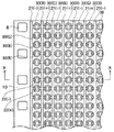
図1は、本発明の発光モジュールを形成するTABテープを利用した配線パターンを有す
る配線基板であり、図2は、この配線基板に発光ダイオードを実装した状態の例を示す平面図であり、図3は、図2におけるX−X断面図である。
Next, the light emitting module of the present invention will be described in detail with reference to the drawings. In the drawings to be referred to, common members are given the same numbering.
FIG. 1 is a wiring board having a wiring pattern using a TAB tape forming a light emitting module of the present invention, and FIG. 2 is a plan view showing an example of a state in which a light emitting diode is mounted on the wiring board. 3 is a sectional view taken along line XX in FIG.
また、図4は、図2おける発光ダイオード30の部分を拡大して示す断面図であり、絶縁基板であるポリイミドフィルム10に形成されたデバイスホール14内に、1個の発光ダイオード(LED)30が実装されている。
4 is an enlarged cross-sectional view showing a portion of the
図2に示す本発明の発光モジュールは、両縁部にスプロケットホール8が形成された絶縁基板10に多数のデバイスホール14が形成され、この個々のデバイスホール14内にはそれぞれ発光ダイオード(LED)30が一個嵌装されている。
In the light emitting module of the present invention shown in FIG. 2, a large number of
発光ダイオード30には、赤く発光するLED30(R)、グリーンに発光するLED30(G)、ブルーに発光するLED30(B)があり、これらを組み合わせるて発光することができる。図2において、最も左側に配置されたLED30は、上から(R),(
B),(G),(R),(B),(G)・・・・・のように発色光の異なるLEDを順次配置されている。また、左から二列目では、最も左列のLEDの配列と同じ順序でLEDが配置されているが、位相が一つだけずらしてLEDが配置されており、同様にこれに隣接する列のLEDも隣接する列のLEDと位相をずらしてLEDが配置されている。
The
LEDs with different colored light are sequentially arranged as in B), (G), (R), (B), (G). Further, in the second column from the left, the LEDs are arranged in the same order as the arrangement of the LEDs in the leftmost column, but the LEDs are arranged with a phase shift of only one, and similarly, the columns adjacent to this are arranged. The LEDs are also arranged with a phase shift from the LEDs in the adjacent rows.
LEDは、上記のように各列が(R),(B),(G)の順列を繰り返すように配置し
てもよいし、任意の一列を(R)の列とし、これに隣接する一列を(B)列、とし、さらにこの(B)列に隣接する列を(G)列とするように列ごとに異なる発色光の発光ダイオードを配列することもできる。
The LEDs may be arranged so that each row repeats the permutation of (R), (B), (G) as described above, or any one row is a row of (R), and one row adjacent to this. It is also possible to arrange light emitting diodes of different colored light for each column so that the column (B) is the column (B) and the column adjacent to the column (B) is the column (G).
また、全てのデバイスホールに青色LEDおよび/または紫外LEDを配置して、このLEDの上に青色光あるいは紫外線を可視光に変換する蛍光体を例えば出光樹脂部38に配置してLEDからの光を白色光にする場合には、全てのデバイスホールに青色LEDあるいは紫外LEDを実装することにより、本発明の発光モジュールとすることができる。
In addition, blue LEDs and / or ultraviolet LEDs are arranged in all device holes, and a phosphor that converts blue light or ultraviolet light into visible light is arranged on the LEDs, for example, in the light-emitting
図1および図2に示すように、このような発光モジュールの絶縁基板10の一方の面には、付番21(−)、21(+)で表わされる配線パターンが交互に形成されており、た
とえば配線パターン21(−)あるいは配線パターン21(+)からは、デバイスホール
14内部に、それぞれ放熱性インナーリード22(−)あるいは放熱性インナーリード22(+)が延設されている。ここで、配線パターン21(+)あるいは21(−)からの
放熱性インナーリード22(+)あるいは22(−)の長さT2は、LED30からの光の放出を妨げず、かつLED30が発光することにより生ずる熱を効率よく吸熱して配線パターン21(+)あるいは21(−)を介して排熱するように設定されるが、通常、LE
D30の長さ(W)は0.1〜0.4mmであり、LED30の中央部にある発光部(図示
なし)の幅は0.05〜0.30mmであることから、放熱性インナーリード22(+)あ
るいは22(−)は、できるだけ線幅が広い方が望ましいが、過度に線幅を広くすると、LEDの開口部を不割くため、熱伝導と放射面積の関係で最適値の範囲を設定することが望ましい。この放熱性インナーリード22(+)あるいは22(−)の長さT2は、できるだけ端に形成され、できるだけ小さく設計して、LED電極に届くぎりぎりの長さであればよく、通常は、0.01〜0.2mm、好ましくは0.05〜0.15mmの範囲内に設定される。
As shown in FIGS. 1 and 2, wiring patterns represented by reference numerals 21 (−) and 21 (+) are alternately formed on one surface of the insulating
The length (W) of D30 is 0.1 to 0.4 mm, and the width of the light emitting portion (not shown) at the center of the
本発明における放熱性インナーリード22(−)あるいは放熱性インナーリード22(+)は、表面にメッキ層を有しており、このメッキ層から供給される金属と、LED30に形成されたバンプ電極32、33から供給される金属とによって放熱性インナーリードと電気的に接合している。
The heat dissipating inner lead 22 (−) or the heat dissipating inner lead 22 (+) in the present invention has a plating layer on the surface, and the metal supplied from the plating layer and the
放熱性インナーリード22(−)あるいは放熱性インナーリード22(+)は、従来のデバイスホールに形成されているフライングインナーリードとは異なり、デバイスホール内に挿入された一つのLED30を、デバイスホール14の両端から延設された二本のフライングインナーリードで接合して保持するものである。そして、この二本のフライングインナーリードによって、LED30は電気的に接合され、しかも回路部材として保持され、さらにLED30が駆動することにより発生する熱を排出する。このために、本発明の発光モジュールに形成されている二本のフライングインナーリードである放熱性インナーリード22(−)および放熱性インナーリード22(+)は、より多くの熱を配線パタ
ーンを介して放熱すると共に、LED30を物理的に保持し、かつLED30を確実に電気的に接続するために、従来のフライングインナーリードとは異なり、非常に太くしかも堅牢に形成されている。通常の場合、LED30の端部には接点部が形成されており、放熱性インナーリードは、この接点部を含めたLED30の端部(片側)の60%以上と接触させることにより、非常に効率的にLED30で発生した熱を放熱性インナーリードから配線パターンへと移行させて排熱することができる。
The heat dissipating inner lead 22 (−) or the heat dissipating inner lead 22 (+) is different from the flying inner lead formed in the conventional device hole, and one
本発明において、LED30には、2個のバンプ電極32,33が形成されており、上記のような放熱性インナーリード22(−)および放熱性インナーリード22(+)の表
面に形成されたメッキ層から供給される金属と、LED30のバンプ電極32,33から供給される金属とによって、LED30と放熱性インナーリード22(−)および放熱性インナーリード22(+)とが電気的に接続される。ここでバンプ電極32.33を形成
する金属としては、金、銀、半田金属、鉛フリー半田金属などを挙げることができ、また放熱性インナーリードの表面に形成されているメッキ層としては、金メッキ層、銀メッキ層、金-ニッケルメッキ層、錫メッキ層、ニッケルメッキ層、半田メッキ層、鉛フリー半
田メッキ層などを挙げることができる。特に本発明においては、LED30のバンプ32,33を形成する金属が金または金合金であることが好ましく、放熱性インナーリードの表面に形成されているメッキ層としては、錫メッキ層が好ましい、このように金バンプを有するLED30を用い、錫メッキ層を有する放熱性インナーリードから錫を溶出させることにより、接合点で金錫共晶物が形成され、多数のLED30と多数の放熱性インナーリードとを一括して強固にボンディングすることができる。
In the present invention, two
本発明において、放熱性インナーリード21の幅T1は、LED30の幅T0を100%
としたときに、このLED30の幅T0に対して通常は20〜100%の範囲内、好まし
くは30〜70%の範囲内になるように形成する。また、この放熱性インナーリード22のデバイスホールからの長さは、デバイスの一片の長さLを100%としたときにデバイスを覆う長さは30%以下、好ましくは10〜30%、特に好ましくは10〜20%の範囲内に設定される。本発明の発光モジュールにおいて、図3に示すように、放熱性インナーリード22(−)、22(+)と接合しているLED30面が発光面となるために、放
熱性インナーリード22(−)、22(+)によって覆われる面を上記のようにすること
により、LED30で発光した光をより有効に外部に取り出すことができる。
In the present invention, the width T 1 of the heat dissipating
In this case, the
本発明において、形成されるデバイスホール14は、LED30の大きさよりも一辺が50μm以上大きいもの、厚さはLEDの厚さと略一致あるいは多少厚くしたポリイミドの厚さを採用する。
In the present invention, the
さらに、図3、図4に示すように、LED30を実装したデバイスホール14の下面に反射板36、好ましくは絶縁性反射板36を貼着することにより、デバイスホール内に実装されたLED30から発せられた光を非常に高い効率で取り出すことができる。このような反射板36としては、アルミニウム箔、あるいは、表面に樹脂コーティングしたアルミニウム箔のような樹脂コート金属箔を挙げることができる。なお、この反射板36を貼着する際の接着剤としては、エポキシ樹脂のような熱硬化性接着剤を使用することが好ましく、この熱硬化性接着剤を接着剤として使用するとともに、この熱硬化性接着剤の硬化体を金属箔の絶縁性被膜として使用することもできる。
Further, as shown in FIG. 3 and FIG. 4, by attaching a
また、上記のようにしてLED30を実装した後、デバイスホール14の放熱性インナーリードが形成されている側(出力面)から透明樹脂を充填して図3、図4に示すように盛り上げて出光樹脂部38を形成することにより、デバイスホール内で発光した光を広角に発散させることができる。また、このように透明樹脂を充填することにより、LED30と放熱性インナーリード22(−)および放熱性インナーリード22(+)との接合強
度も高くなる。
In addition, after mounting the
このように出光樹脂部38として使用する透明樹脂としては透明性および耐熱性が高い樹脂を使用することができ、このような樹脂の例としては、熱または光硬化性のアクリル樹脂、エポキシ樹脂などを挙げることができる。これらは単独であるいは組み合わせて使用することができる。
As described above, a resin having high transparency and heat resistance can be used as the transparent resin used as the light-emitting
上記のような本発明の発光モジュールは、たとえば図5に示すようにして製造することができる。
図5に示す例では、先ず、図5(a)に示すように接着剤層12付き絶縁基板10を用意する。
The light emitting module of the present invention as described above can be manufactured, for example, as shown in FIG.
In the example shown in FIG. 5, first, an insulating
ここで使用する絶縁基板10としては、良好な耐熱性を示し、かつ耐水性、耐薬品性に優れた樹脂から形成された絶縁基板が好ましい。このような絶縁基板としては、ポリイミド基板、ポリアミドイミド基板、エポキシ樹脂基板、フェノール樹脂基板、BTレジン基板、液晶樹脂基板などを挙げることができる。これらの中でも、たいへん優れた耐熱性を示すとともに、可撓性をも有するポリイミドフィルムからなる絶縁基板が好ましい。
The insulating
本発明で使用する絶縁基板10は、デバイスホール14内にLED30を収納して使用することから、LED30を収納するに足りる厚さを有していることが必要であり、通常は50〜250μm、好ましくは70〜125μmの厚さのポリイミドフィルムを使用する。
Since the insulating
この絶縁基板の一方の面には接着剤層12が備えられている。この接着剤層12を形成する接着剤は、熱硬化性の接着剤であることが好ましく、エポキシ樹脂系接着剤、ポリイミド系接着剤、熱硬化性アクリル系接着剤、熱硬化性ウレタン系接着剤などの熱硬化性接着剤を使用することができる。この接着剤層の厚さは、通常は10〜35μm程度である。
An
上記のような接着剤層12付き絶縁基板10を用いて、図5(b)に示すように、多数のデバイスホール14を形成する。デバイスホールの形成間隔は、図1に示すように、多数のLEDを配置し、デバイスホール14の間にLED30に電力を供給するための配線パターン21を形成する間隙を残してできるだけ密に形成することが好ましい。
A large number of device holes 14 are formed using the insulating
形成するデバイスホール14の形状は、LED30を収納できる形状であれば、方形であっても、円形であっても、その他の形状であってもよい。
図1には、幅35mmのポリイミドフィルムを用いた例が示されており、図1は、このポリイミドフィルムの両側にはスプロケットホール8が形成され、この両側のスプロケットホール8との間の25mmの幅を有する絶縁基板に直径0.5mmの円形のデバイスホール14が多数形成され、デバイスホール14の間に配線パターン21(−)、21(+)が形
成された配線基板の例である。
The shape of the
FIG. 1 shows an example using a polyimide film having a width of 35 mm. FIG. 1 shows that a
デバイスホール14の形成には、レーザー光等を使用することもできるが、パンチングによるのが効率的である。なお、このパンチングに際して、絶縁基板10テープの両縁部にスプロケットホール8を穿設する。このスプロケットホール8は、このテープの搬送に利用するとともに、テープの位置決手段としても利用することができる。
Laser light or the like can be used to form the
上記のようにして所定のデバイスホール14を穿設した後の接着剤層12付き絶縁基板10金属箔を接着する。ここで使用することができる金属としては、導電性および熱伝導性に優れ、しかもエッチングにより容易に加工することができる金属を使用する。このような金属の例としては、銅、アルミニウム、錫、金、銀を挙げることができるが、加工性および経済性から銅を使用することが好ましい。本発明で銅を使用する場合、銅合金であってもよい。
The metal foil of the insulating
本発明で金属箔20として銅を使用する場合、銅箔には、電解銅箔および圧延銅箔があるが、本発明ではいずれの銅箔を使用することも可能である。ただし、絶縁基板10との接着強度を考慮すると、電解銅箔を使用することが好ましい。この電解銅箔20には、銅の析出が始まるシャイニー面(S面)と、銅の析出が終了するマット面(M面)とがあるが、接着剤層12付き絶縁基板10の接着剤層12と、電解銅箔のマット面(M面)とが対峙するように両者を配置して、加熱下に加圧することにより、図5(c)に示すような銅張り積層板を得ることができる。
When copper is used as the
ここで使用することができる金属箔20、好ましくは電解銅箔20の厚さに特に制限はないが、本発明の発光モジュールにおいて、この金属箔20あるいは電解銅箔20によって形成される配線パターンが、LED30に電力を供給するだけでなく、LED30で発生した熱をモジュールの外に排熱する熱伝導体も兼ねていることから、比較的厚い金属箔20を使用することが好ましい。このような金属箔として電解銅箔を使用する場合、20〜150μm程度の電解銅箔を使用することができるが、特に本発明では、50〜100μmの電解銅箔を使用することが好ましい。このような厚さの電解銅箔20を用いて形成された配線パターンは、良好な熱伝導性を有するとともに、通電の際の電気抵抗も低いので、LED30を駆動させるために電力を供給する際に配線パターン21自体が発熱することがない。また、本発明の発光モジュールでは、デバイスホール14内に一対のフライングリードである放熱性インナーリード22(+)、22(−)を形成して、LED30
と接続して、このLED30を保持する際に、上記のような厚さの電解銅箔を使用することにより、LED30を実装したことによって、放熱性インナーリード22(+)、22
(−)が折れ曲がることながなく、また変形すらも生じない非常に強靭なインナーリードを形成することができる。
The thickness of the
When the
It is possible to form a very tough inner lead that does not bend (−) and does not even deform.
金属箔を20をエッチングして配線パターン21(−)と配線パターン21(+)およ
び配線パターン21(−)に接続した放熱性インナーリード22(−)と配線パターン21(+)に接続した放熱性インナーリード22(−)を形成する。
Heat radiation connected to the wiring pattern 21 (+) and the heat dissipating inner lead 22 (-) connected to the wiring pattern 21 (-) and the wiring pattern 21 (-) by etching the
即ち、デバイスホール14内、および、電解銅箔20の表面の配線パターン21(−)とこの配線パターン21(−)に接続した放熱性インナーリード22(−)、および、電解銅箔20の表面の配線パターン21(+)とこの配線パターン21(+)に接続した放熱性インナーリード22(+)の部分に感光性樹脂の硬化体からなるマスキング材23を形
成して、このマスキング材23から露出した電解銅箔20および無電解銅メッキ層をエッチングする。ここで使用するエッチング剤としては、塩化第2鉄、塩化第2銅、硫酸第2鉄、硫酸第2銅などを主剤とする通常のエッチング剤を使用することができる。
That is, in the
このようにしてエッチングすることにより、マスキング材23が形成されていない金属箔20のが除去されて、配線パターン21(−)とこの配線パターン21(−)に接続した放熱性インナーリード22(−)、および、電解銅箔20の表面の配線パターン21(+)とこの配線パターン21(+)に接続した放熱性インナーリード22(+)の部分を残
して金属箔20が除去され、LED30からの光が出る開口部24が形成される。
By etching in this way, the
上記のようにエッチングを行った後、マスキング材は、水酸化ナトリウム水溶液などのアルカリ水溶液で洗浄することにより除去することができる。
こうしてマスキング材23が除去された配線基板を図5(f)に示す。
After etching as described above, the masking material can be removed by washing with an aqueous alkali solution such as an aqueous sodium hydroxide solution.
The wiring board from which the masking
次いで、こうして形成された配線基板を、図5(g)に示すように、錫メッキ層18を形成する。この錫メッキ層は、無電解メッキ法によって形成されることから、エッチングすることによって形成された配線パターンおよびインナーリードの表面に形成される。
Next, a
このように錫メッキ層を形成することにより、LED30のバンプ電極32,33から供給される金と、インナーリードの表面に形成される錫メッキ層から供給される錫とによって金錫共晶化合物を形成することにより、インナーリードとLED30とを強固に接合することができる。
By forming the tin plating layer in this manner, the gold-tin eutectic compound is formed by the gold supplied from the
このような錫メッキ層の厚さは、通常は0.3〜10μm、好ましくは0.5〜10μmの範囲内になる。
上記のようにして錫メッキ層を形成した後、LED30を実装する。LED30には、通常は、プラス極に金バンプが形成され、マイナス極にも金バンプが形成されている。また、インナーリードの表面には、錫が存在することから、金錫共晶が形成されて、LED30が強固に一括してインナーリードに接合する。
The thickness of such a tin plating layer is usually in the range of 0.3 to 10 μm, preferably 0.5 to 10 μm.
After forming the tin plating layer as described above, the
すなわち本発明においては、各デバイスホール14にそれぞれ1個のLED30を挿入
した後、複数のLED30を、それぞれのデバイスホール14に形成された放熱性インナーリード22に一括して接合させることができる。
That is, in the present invention, after one
上記のようにLED30とインナーリードとを電気的に接合した後、絶縁基板10の表面に反射板を貼着することが好ましい。ここで使用する反射板としては、アルミニウム箔、銅箔等の金属箔、表面を絶縁処理した前記金属箔など挙げることができる。また、この金属箔を貼着する際に使用する接着剤を絶縁層として使用することができる。このように使用される反射板の厚さは通常は10〜100μm、好ましくは20〜50μmの範囲内にある。また、ここで使用する接着剤は熱硬化型の接着剤を使用することが好ましく、通常は、エポキシ樹脂系接着剤、ポリイミド樹脂系接着剤、熱硬化性アクリル系接着剤などを使用することができ、この接着剤層の厚さは通常は5〜50μm、好ましくは10〜20μmである。
After the
上記のように反射板36を裏面に貼着した後、デバイスホール14の放熱性インナーリードが形成されている開口部24から透明樹脂を充填して出光樹脂部38を形成する。ここで、使用する透明樹脂としては、アクリル樹脂、エポキシ樹脂などを挙げることができる。このような樹脂から形成される出光樹脂部38は、その表面形状がドーム型になるように盛り上げることにより、出光樹脂部38からの光を広角に拡散させることができる。この出光樹脂部38を形成する樹脂も、熱硬化性樹脂を使用することが好ましい。
After sticking the reflecting
また、青色ダイオードあるいは紫外ダイオードを使用する場合には、たとえばこの出光樹脂部38に蛍光剤を配合することにより、青色光あるいは紫外光を白色光に変換することができる。
When a blue diode or an ultraviolet diode is used, blue light or ultraviolet light can be converted into white light by, for example, blending a fluorescent agent with the light emitting
上記のように、本発明の発光モジュールは、LED30をデバイスホール14内に収納し錫メッキ層18とが形成されているので、デバイスホール14内に実装されたLED30から発生する熱を放熱性インナーリード22(−)、22(+)を通して配線パターン
21を介して放出するとともに、デバイスホール14内に配置されたLED30から発生してデバイスホールの熱エネルギーを、底部に貼り合わせた反射板36である金属シートを介して排出することができる。
As described above, since the
しかも、本発明の発光モジュールは、従来の発光モジュールのようにワイヤーボンディングでLED30を接合しておらず、LEDに形成されたバンプを用いたボンデイングによりTABテープ型の基板のデバイスホール内に配置した複数のLED30を放熱性インナーリードに一括ボンディングにより、実装することができるので、ボンデイング効率が高く、容易に本発明の発光モジュールを製造することができる。
Moreover, the light emitting module of the present invention does not join the
即ち、本発明では、多数のデバイスホールにそれぞれ1個のLEDを挿入し、このよう
にLEDが挿入された多数のデバイスホールとLEDとに、デバイスホールの数に対応した個数のボンダーを当接して、超音波をかけながら加熱し、さらに必要により加圧することにより、多数のLEDを一回のボンディング操作で実装することができる。従って、非常に効率よくLEDを実装することができる。
That is, in the present invention, one LED is inserted into each of a large number of device holes, and a number of bonders corresponding to the number of device holes are brought into contact with the large number of device holes and LEDs into which the LEDs are thus inserted. Then, by applying heat while applying ultrasonic waves and further applying pressure as necessary, a large number of LEDs can be mounted by a single bonding operation. Therefore, the LED can be mounted very efficiently.
本発明の光モジュールは、LEDからの光のほとんどの部分が出光樹脂部38が射出されることができる。従って、本発明の発光モジュールは、非常に効率がよく、しかも温度が高くならないという特性を有している。
In the optical module of the present invention, most of the light from the LED can be emitted from the light emitting
次に本発明の実施例を示して本発明の配線基板および発光モジュールについて、詳細に説明するが、本発明はこれらによって限定されるものではない。 Next, although the Example of this invention is shown and the wiring board and light emitting module of this invention are demonstrated in detail, this invention is not limited by these.
〔実施例1〕
厚さ75μmのポリイミドフィルムの一方の面にポリイミド前駆体からなる接着剤層を有する接着剤層付きポリイミドフィルムを用意した。
[Example 1]
A polyimide film with an adhesive layer having an adhesive layer made of a polyimide precursor on one surface of a polyimide film having a thickness of 75 μm was prepared.
この接着剤層付きポリイミドフィルムに、直径L3が0.5mmの円形のデバイスホー
ルを多数形成した。
This adhesive layer with the polyimide film, the diameter L 3 to form a number of circular device hole of 0.5 mm.
この接着剤層付きポリイミドフィルムに、平均厚さが35μmの電解銅箔を、電解銅箔のマット面が接着剤層と対面するように配置して、加熱下に加圧て積層体を形成した。
次に、デバイスホール層の内周面、配線パターンを形成する電解銅箔面に、感光性樹脂を用いて得して、露光・現像してマスキング材を形成した。
On this polyimide film with an adhesive layer, an electrolytic copper foil having an average thickness of 35 μm was placed so that the mat surface of the electrolytic copper foil faces the adhesive layer, and pressed under heating to form a laminate. .
Next, a masking material was formed by using a photosensitive resin on the inner peripheral surface of the device hole layer and the electrolytic copper foil surface on which the wiring pattern was formed, and exposing and developing.
こうしてマスキング材を形成した積層体をエッチング剤に浸漬してマスキング材が形成されていない部分の金属を除去し、アルカリ洗浄してマスキング材を除去した。
こうしてマスキング材を除去した後、無電解錫メッキを行い、金属の表面に錫メッキ層を形成した。
Thus, the laminated body which formed the masking material was immersed in the etching agent, the metal of the part in which the masking material was not formed was removed, and the masking material was removed by alkali washing.
After removing the masking material in this manner, electroless tin plating was performed to form a tin plating layer on the metal surface.
次いで、デバイスホール14にLED30を挿入して、超音波加熱でデバイスホール14内にLEDのバンプ電極とインナーリードの錫とを利用して一括ボンディングにより金錫共晶物を形成して、LEDをインナーリードに電気的に固定した。
Next, the
こうしてLEDを固定した後、裏面側に表面に絶縁加工したアルミニウム箔をエポキシ樹脂を用いて貼着した。
さらに、インナーリードが形成されている側に、熱硬化性アクリル樹脂で封止して出光樹脂部を形成した。
After fixing the LED in this manner, an aluminum foil having an insulating process on the front surface was attached to the back surface using an epoxy resin.
Further, the light emitting resin portion was formed by sealing with a thermosetting acrylic resin on the side where the inner lead was formed.
このようにして形成された発光モジュール9個に約1Wの電力を供給して、本発明の発光モジュールからの光量、および、発光モジュールの温度を測定した。
市販のLED素子9個を並べて、同様にして発光モジュールを形成して、光量、および温度を対比した。結果を次表に記載する。
The power of about 1 W was supplied to the nine light emitting modules thus formed, and the amount of light from the light emitting module of the present invention and the temperature of the light emitting module were measured.
Nine commercially available LED elements were arranged, a light emitting module was formed in the same manner, and the amount of light and temperature were compared. The results are listed in the following table.

本発明の発光モジュールによれば、電極リードからも熱が伝導するため、発光モジュールの温度が高くならない。従って、本発明の発光モジュールは高密度でLEDを実装することができ、単位面積当たりの発光量が高く、しかも発光量に比し温度上昇が少ないとの特性を有している。従って、本発明の発光モジュールは、従来から使用されている白熱灯、蛍光灯などとは別の新たな第三の光源として使用することが可能となった。 According to the light emitting module of the present invention, heat is conducted also from the electrode leads, so the temperature of the light emitting module does not increase. Therefore, the light emitting module of the present invention has the characteristics that LEDs can be mounted at high density, the light emission amount per unit area is high, and the temperature rise is small compared to the light emission amount. Therefore, the light emitting module of the present invention can be used as a new third light source different from the incandescent lamps and fluorescent lamps conventionally used.
8・・・・スプロケットホール
10・・・絶縁基板
12・・・接着剤層
14・・・デバイスホール
18・・・錫メッキ層
20・・・銅箔(電解銅箔)
21・・・配線パターン
22・・・放熱性インナーリード
23・・・マスキング材
24・・・開口部
30・・・発光ダイオード(LED)
32・・・バンプ電極
33・・・バンプ電極
36・・・反射板(金属シート)
38・・・出光樹脂部
8 ...
21 ...
32 ...
38 ... Idemitsu resin part
Claims (9)
ことを特徴とする請求項第1項記載の発光モジュール。 2. The light emitting module according to claim 1, wherein the insulating substrate is a polyimide film having an average thickness in the range of 50 to 300 [mu] m.
ることを特徴とする請求項第1項記載の発光モジュール。 2. The wiring pattern and the heat dissipating inner lead are formed by etching a copper foil having an average thickness of 12 to 120 [mu] m adhered to a polyimide film with an adhesive layer. The light emitting module as described.
Priority Applications (1)
| Application Number | Priority Date | Filing Date | Title |
|---|---|---|---|
| JP2008144316A JP2009290167A (en) | 2008-06-02 | 2008-06-02 | Light emitting module |
Applications Claiming Priority (1)
| Application Number | Priority Date | Filing Date | Title |
|---|---|---|---|
| JP2008144316A JP2009290167A (en) | 2008-06-02 | 2008-06-02 | Light emitting module |
Publications (1)
| Publication Number | Publication Date |
|---|---|
| JP2009290167A true JP2009290167A (en) | 2009-12-10 |
Family
ID=41459050
Family Applications (1)
| Application Number | Title | Priority Date | Filing Date |
|---|---|---|---|
| JP2008144316A Pending JP2009290167A (en) | 2008-06-02 | 2008-06-02 | Light emitting module |
Country Status (1)
| Country | Link |
|---|---|
| JP (1) | JP2009290167A (en) |
Cited By (7)
| Publication number | Priority date | Publication date | Assignee | Title |
|---|---|---|---|---|
| WO2011077899A1 (en) * | 2009-12-25 | 2011-06-30 | 富士フイルム株式会社 | Insulating substrate and light emitting element |
| KR101240943B1 (en) | 2011-07-25 | 2013-03-11 | 교우세라 커넥터 프로덕츠 가부시키가이샤 | Module for attaching LED, LED module, Fabricating method of module for attaching LED and Fabricating method of LED module |
| JP2014078686A (en) * | 2012-08-31 | 2014-05-01 | Nichia Chem Ind Ltd | Light emitting device and manufacturing method of the same |
| JP2015511393A (en) * | 2011-06-15 | 2015-04-16 | 長塚 康弘 | Flexible circuit assembly and method thereof |
| WO2015186566A1 (en) * | 2014-06-02 | 2015-12-10 | 株式会社ヴィーネックス | Line light source and optical line sensor unit |
| WO2016104609A1 (en) * | 2014-12-25 | 2016-06-30 | 大日本印刷株式会社 | Led element substrate, led-mounted module and led display device using these |
| JP2016122815A (en) * | 2014-12-25 | 2016-07-07 | 大日本印刷株式会社 | Substrate for LED element |
Citations (5)
| Publication number | Priority date | Publication date | Assignee | Title |
|---|---|---|---|---|
| JPS63173670A (en) * | 1987-01-13 | 1988-07-18 | Alps Electric Co Ltd | Light-emitting diode array head and manufacture thereof |
| JPS63296346A (en) * | 1987-05-28 | 1988-12-02 | Hitachi Cable Ltd | Film carrier for semiconductor device |
| JPH10261674A (en) * | 1997-01-16 | 1998-09-29 | Toshiba Corp | Semiconductor device and fabrication therefor |
| JP2007129188A (en) * | 2005-10-07 | 2007-05-24 | Hitachi Maxell Ltd | Semiconductor device, semiconductor module, and method of manufacturing the semiconductor module |
| WO2007063971A1 (en) * | 2005-12-02 | 2007-06-07 | Matsushita Electric Industrial Co., Ltd. | Communication system, server, and information processing terminal |
-
2008
- 2008-06-02 JP JP2008144316A patent/JP2009290167A/en active Pending
Patent Citations (5)
| Publication number | Priority date | Publication date | Assignee | Title |
|---|---|---|---|---|
| JPS63173670A (en) * | 1987-01-13 | 1988-07-18 | Alps Electric Co Ltd | Light-emitting diode array head and manufacture thereof |
| JPS63296346A (en) * | 1987-05-28 | 1988-12-02 | Hitachi Cable Ltd | Film carrier for semiconductor device |
| JPH10261674A (en) * | 1997-01-16 | 1998-09-29 | Toshiba Corp | Semiconductor device and fabrication therefor |
| JP2007129188A (en) * | 2005-10-07 | 2007-05-24 | Hitachi Maxell Ltd | Semiconductor device, semiconductor module, and method of manufacturing the semiconductor module |
| WO2007063971A1 (en) * | 2005-12-02 | 2007-06-07 | Matsushita Electric Industrial Co., Ltd. | Communication system, server, and information processing terminal |
Cited By (8)
| Publication number | Priority date | Publication date | Assignee | Title |
|---|---|---|---|---|
| WO2011077899A1 (en) * | 2009-12-25 | 2011-06-30 | 富士フイルム株式会社 | Insulating substrate and light emitting element |
| JP2015511393A (en) * | 2011-06-15 | 2015-04-16 | 長塚 康弘 | Flexible circuit assembly and method thereof |
| KR101240943B1 (en) | 2011-07-25 | 2013-03-11 | 교우세라 커넥터 프로덕츠 가부시키가이샤 | Module for attaching LED, LED module, Fabricating method of module for attaching LED and Fabricating method of LED module |
| JP2014078686A (en) * | 2012-08-31 | 2014-05-01 | Nichia Chem Ind Ltd | Light emitting device and manufacturing method of the same |
| WO2015186566A1 (en) * | 2014-06-02 | 2015-12-10 | 株式会社ヴィーネックス | Line light source and optical line sensor unit |
| JPWO2015186566A1 (en) * | 2014-06-02 | 2017-04-20 | 株式会社ヴィーネックス | Line light source and optical line sensor unit |
| WO2016104609A1 (en) * | 2014-12-25 | 2016-06-30 | 大日本印刷株式会社 | Led element substrate, led-mounted module and led display device using these |
| JP2016122815A (en) * | 2014-12-25 | 2016-07-07 | 大日本印刷株式会社 | Substrate for LED element |
Similar Documents
| Publication | Publication Date | Title |
|---|---|---|
| EP2648238B1 (en) | Light-emitting element mounting package, and manufacturing method of the same | |
| JP4910220B1 (en) | LED module device and manufacturing method thereof | |
| JP2005050838A (en) | Surface mounted led and light emitting device employing it | |
| JP2013033911A (en) | Substrate for mounting light emitting element and led package | |
| JP2004172170A (en) | High luminance light emitting device and method of manufacturing the same | |
| JP2009290167A (en) | Light emitting module | |
| JP2006005290A (en) | Light emitting diode | |
| KR100787705B1 (en) | Embedded metal heat sink for semiconductor device and method for manufacturing the same | |
| JP2013033909A (en) | Substrate for mounting light emitting element and led package | |
| JP2010109119A (en) | Light emitting module, and method of manufacturing the same | |
| JP2009054801A (en) | Heat radiation member, and light emitting module equipped with the same | |
| US9425373B2 (en) | Light emitting module | |
| JP2015111620A (en) | Light emitting device and manufacturing method of the same | |
| JP2013149947A (en) | Package for mounting light emitting element, light emitting element package, and manufacturing methods of package for mounting light emitting element and light emitting element package | |
| JP2007287751A (en) | Light emitting device | |
| JP2006278766A (en) | Mount structure and mount method of light-emitting element | |
| JP5812845B2 (en) | Light-emitting element mounting package, light-emitting element package, and manufacturing method thereof | |
| JP2014220472A (en) | Wiring board and light-emitting device using the same | |
| JP2010092973A (en) | Electronic component | |
| JP2023166372A (en) | Method of manufacturing light-emitting device, and light-emitting device | |
| EP2642835A2 (en) | Wiring board device, luminaire, and manufacturing method of the wiring board device | |
| KR100610275B1 (en) | Power LED package and method for producing the same | |
| KR101719692B1 (en) | Printed Circuit Board, Manufacturing method thereof, LED module and LED lamp with using the same | |
| JP2009021384A (en) | Electronic component and light emitting device | |
| EP2642836A2 (en) | Wiring board device, luminaire and manufacturing method of the wiring board device |
Legal Events
| Date | Code | Title | Description |
|---|---|---|---|
| A621 | Written request for application examination |
Free format text: JAPANESE INTERMEDIATE CODE: A621 Effective date: 20110509 |
|
| RD02 | Notification of acceptance of power of attorney |
Free format text: JAPANESE INTERMEDIATE CODE: A7422 Effective date: 20120223 |
|
| A131 | Notification of reasons for refusal |
Free format text: JAPANESE INTERMEDIATE CODE: A131 Effective date: 20120612 |
|
| A977 | Report on retrieval |
Free format text: JAPANESE INTERMEDIATE CODE: A971007 Effective date: 20120613 |
|
| A02 | Decision of refusal |
Free format text: JAPANESE INTERMEDIATE CODE: A02 Effective date: 20121016 |