JP2009265406A - Display device and electronic appliance - Google Patents
Display device and electronic appliance Download PDFInfo
- Publication number
- JP2009265406A JP2009265406A JP2008115769A JP2008115769A JP2009265406A JP 2009265406 A JP2009265406 A JP 2009265406A JP 2008115769 A JP2008115769 A JP 2008115769A JP 2008115769 A JP2008115769 A JP 2008115769A JP 2009265406 A JP2009265406 A JP 2009265406A
- Authority
- JP
- Japan
- Prior art keywords
- refractive index
- display device
- light
- light emitting
- high refractive
- Prior art date
- Legal status (The legal status is an assumption and is not a legal conclusion. Google has not performed a legal analysis and makes no representation as to the accuracy of the status listed.)
- Pending
Links
Images


Landscapes
- Liquid Crystal (AREA)
- Devices For Indicating Variable Information By Combining Individual Elements (AREA)
- Electroluminescent Light Sources (AREA)
- Optical Elements Other Than Lenses (AREA)
Abstract
Description
本発明は、配光特性をもつ表示光を出射する表示装置、およびそのような表示装置を備えた電子機器に関する。 The present invention relates to a display device that emits display light having light distribution characteristics, and an electronic device including such a display device.
有機EL(ElectroLuminescence)素子やLED(Light Emitting Diode)などの自発光素子を用いた表示装置や光源装置において、光利用効率を向上させるため、多重反射を用いた共振器構造や反射鏡を用いた構造が提案され、実現されている。しかしながら、このような構造を採用した場合、出力光の配光分布において指向性が強くなる場合が多く、このような配光特性は表示装置としては好ましいものではない。特に、斜め方向から見たときの輝度の急激な低下や色ずれ(視野角特性)などは、表示画質を著しく低下させる原因となる。 In display devices and light source devices using self-luminous elements such as organic EL (ElectroLuminescence) elements and LEDs (Light Emitting Diodes), a resonator structure or reflector using multiple reflections was used to improve light utilization efficiency. A structure has been proposed and realized. However, when such a structure is adopted, the directivity is often strong in the light distribution of the output light, and such a light distribution characteristic is not preferable for a display device. In particular, a sharp decrease in luminance or color shift (viewing angle characteristics) when viewed from an oblique direction causes a significant decrease in display image quality.
従来、このような視野角特性を改善する方法として、樹脂中にビーズを散布した拡散板や、凹凸形状の表面からなる散乱板を用いる方法などがある。これらは、入射光に対して、均一な作用(拡散作用または散乱作用)を与えるものである。したがって、視野角分布に対する均一性を上げるためには、ビーズもしくは凹凸形状表面に対して臨界角以上の光入射の割合を増やし、入射光にケラレが生じることが必要となる。 Conventionally, as a method for improving such viewing angle characteristics, there are a method of using a diffusion plate in which beads are dispersed in a resin, or a scattering plate having an uneven surface. These give uniform action (diffuse action or scattering action) to incident light. Therefore, in order to increase the uniformity with respect to the viewing angle distribution, it is necessary to increase the proportion of light incident at a critical angle or more with respect to the bead or the uneven surface and to cause vignetting in the incident light.
ところが、そのようにケラレを生じさせた場合には、臨界角以上の光入射の割合が増えるため、輝度低下が生じる。このような輝度低下は消費電力の増大や電流密度の上昇を引き起こすことから、表示装置や光源装置に対する負荷が増大してしまうことになる。 However, when vignetting is caused in such a manner, the ratio of light incidence exceeding the critical angle increases, resulting in a decrease in luminance. Such a decrease in luminance causes an increase in power consumption and an increase in current density, which increases the load on the display device and the light source device.
また、散乱作用が非常に強い拡散板や散乱板を表示装置に適用した場合には、その散乱作用が強いことに起因して、表示画像のぼけやにじみ、反射光の増大といった問題が新たに発生する。したがって、表示装置への適用を考えた場合、鮮明な映像を提供することが困難となってしまう。 In addition, when a diffusing plate or scattering plate having a very strong scattering action is applied to a display device, problems such as blurring and blurring of the display image and an increase in reflected light are newly caused by the strong scattering action. appear. Therefore, when considering application to a display device, it becomes difficult to provide a clear image.
一方、近年では、角度選択性を有する異方性散乱フィルムが提案されている(例えば、特許文献1参照)。これは、フィルムの法線方向(厚み方向)に一定の屈折率をもつと共に、フィルムの面内方向に異なる屈折率の領域を設けるようにしたものである。このような面内方向の屈折率差により、全反射による散乱作用と透過作用とを生じさせ、上記した角度選択性を有するようになっている。 On the other hand, in recent years, anisotropic scattering films having angle selectivity have been proposed (see, for example, Patent Document 1). This has a constant refractive index in the normal direction (thickness direction) of the film and a region having a different refractive index in the in-plane direction of the film. Such a difference in refractive index in the in-plane direction causes a scattering effect and a transmission effect due to total reflection, and has the above-described angle selectivity.
上記特許文献1等で提案されている異方性散乱フィルムでは、従来の拡散板や散乱板と同様の多重反射による散乱作用に加え、面内方向の円柱形状の屈折率領域におけるレンズ効果によって、新たな散乱作用を与えている。ここで、このような円柱形状の屈折率領域におけるレンズ効果は、散乱作用という観点からは、非常に有効であると思われる。しかしながら、このような異方性散乱フィルムを表示装置に適用した場合、前述した拡散板や散乱板と同様に非常に強い画素ぼかしの効果が生じるため、鮮明な映像を提供することが困難となってしまうことになる。
In the anisotropic scattering film proposed in the above-mentioned
なお、これまで述べたような問題は、自発光素子を用いた表示装置だけでなく、液晶素子などを用いた表示装置においても、同様に生じうるものである。 Note that the problems described so far can occur not only in display devices using self-luminous elements, but also in display devices using liquid crystal elements.
本発明はかかる問題点に鑑みてなされたもので、その目的は、正面方向の輝度低下の抑制と視野角特性の向上とを両立させつつ、従来よりも表示画質を向上させることが可能な表示装置および電子機器を提供することにある。 The present invention has been made in view of such a problem, and an object of the present invention is to provide a display capable of improving display image quality as compared with the related art while achieving both reduction in luminance in the front direction and improvement in viewing angle characteristics. It is to provide an apparatus and an electronic device.
本発明の表示装置は、各画素に配置された発光素子と、この発光素子の観察面側に配置され、角度依存の配光特性を有する発光素子からの入射光を散乱させるための異方性散乱層とを備えたものである。ここで、上記異方性散乱層では、面内方向の領域が、複数の高屈折率領域と、これら高屈折率領域よりも屈折率の低い低屈折率領域とから構成されている。また、上記高屈折率領域が、厚み方向から傾斜してなる四角柱状であると共に、この四角柱状の高屈折率領域における矩形断面の一辺が、発光素子の発光面と略平行となっている。 The display device of the present invention includes a light emitting element disposed in each pixel and anisotropy for scattering incident light from the light emitting element disposed on the observation surface side of the light emitting element and having an angle-dependent light distribution characteristic. And a scattering layer. Here, in the anisotropic scattering layer, the region in the in-plane direction includes a plurality of high refractive index regions and a low refractive index region having a lower refractive index than these high refractive index regions. The high refractive index region has a quadrangular prism shape inclined from the thickness direction, and one side of a rectangular cross section in the quadrangular columnar high refractive index region is substantially parallel to the light emitting surface of the light emitting element.
本発明の電子機器は、表示機能を有する上記表示装置を備えたものである。 An electronic apparatus according to the present invention includes the display device having a display function.
本発明の表示装置および電子機器では、角度依存の配光特性を有する発光素子からの入射光が異方性散乱層において散乱され、表示光として出射される。ここで、この異方性散乱層では、面内方向の領域が、厚み方向から傾斜した四角柱状からなる複数の高屈折率領域と上記低屈折率領域とから構成されていることにより、入射光の入射方向に応じて、異方性散乱層では異なる作用がなされる。すなわち、四角柱状の高屈折率領域の傾斜方向からの入射光は、この高屈折率領域内で多重反射され、傾斜方向へ選択的に散乱された表示光となる。また、この傾斜方向以外の方向からの入射光は、高屈折率領域を通過して表示光となる。その際、四角柱状の高屈折率領域における矩形断面の一辺が発光素子の発光面と略平行となっていることにより、従来とは異なり、傾斜方向以外の方向からの入射光が高屈折率領域において散乱されず、入射角を維持したまま出射される。 In the display device and the electronic apparatus of the present invention, incident light from a light emitting element having angle-dependent light distribution characteristics is scattered in the anisotropic scattering layer and emitted as display light. Here, in this anisotropic scattering layer, the region in the in-plane direction is composed of a plurality of high refractive index regions having a quadrangular prism shape inclined from the thickness direction and the low refractive index region. Depending on the incident direction, different actions are performed in the anisotropic scattering layer. That is, the incident light from the tilt direction of the quadrangular prism-shaped high refractive index region is multiple-reflected in the high refractive index region and becomes display light selectively scattered in the tilt direction. Further, incident light from a direction other than the tilt direction passes through the high refractive index region and becomes display light. At that time, since one side of the rectangular cross section in the square columnar high refractive index region is substantially parallel to the light emitting surface of the light emitting element, incident light from a direction other than the inclined direction is different from the conventional one. In this case, the light is emitted without maintaining the incident angle.
本発明の表示装置または電子機器によれば、異方性散乱層において、面内方向の領域を、厚み方向から傾斜した四角柱状からなる複数の高屈折率領域と上記低屈折率領域とから構成するようにしたので、四角柱状の高屈折率領域の傾斜方向に応じて、散乱された表示光を選択的に出射させることができる。また、四角柱状の高屈折率領域における矩形断面の一辺が発光素子の発光面と略平行となるようにしたので、傾斜方向以外の方向からの入射光が散乱されずに入射角を維持したまま出射することができ、従来と比べ、入射光の光量損失を低減する共に、散乱に起因した表示画像のぼけを抑えることができる。よって、正面方向の輝度低下の抑制と視野角特性の向上とを両立させつつ、従来よりも表示画質を向上させることが可能となる。 According to the display device or electronic device of the present invention, in the anisotropic scattering layer, the in-plane direction region is composed of a plurality of high-refractive index regions that are square pillars inclined from the thickness direction and the low-refractive index region. Thus, the scattered display light can be selectively emitted according to the inclination direction of the quadrangular columnar high refractive index region. In addition, since one side of the rectangular cross section in the quadrangular columnar high refractive index region is substantially parallel to the light emitting surface of the light emitting element, incident light from directions other than the tilt direction is not scattered and the incident angle is maintained. As compared with the prior art, the light quantity loss of incident light can be reduced and the blur of the display image due to scattering can be suppressed. Therefore, it is possible to improve the display image quality as compared with the related art while achieving both the reduction in luminance in the front direction and the improvement in viewing angle characteristics.
以下、本発明の実施の形態について、図面を参照して詳細に説明する。 Hereinafter, embodiments of the present invention will be described in detail with reference to the drawings.
図1は、本発明の一実施の形態に係る表示装置(有機EL表示装置1)の断面構成(Z−X断面構成)を表すものである。この有機EL表示装置1では、例えば、ガラスなどよりなる駆動用基板11の上に、後述する複数の発光部16R,16G,16Bがそれぞれ画素10R,10G,10Bにマトリクス状に配置されている。また、駆動用基板11の上には、映像表示用の画素駆動回路である信号線駆動回路や走査線駆動回路(図示せず)が形成されている。具体的には、駆動用基板11と対向基板15との間には、駆動用基板11側から、発光部16R,16G,16B、絶縁層12、保護層13、封止層14、カラーフィルタ層17R,17B,17Gおよびブラックマトリクス層BMが、この順に積層されている。また、対向基板15における駆動用基板11の反対側(観察面側)には、異方性散乱フィルム18(異方性散乱層)が一様に形成されている。
FIG. 1 shows a cross-sectional configuration (ZX cross-sectional configuration) of a display device (organic EL display device 1) according to an embodiment of the present invention. In the organic
発光部16R,16G,16Bはそれぞれ、画素10R,10G,10Gに対応する領域に形成されており、赤色波長領域,緑色波長領域,青色波長領域の光を発する自発光型の発光素子(有機EL素子)により構成されている。図2は、この有機EL素子の断面構成(Z−X断面構成)を詳細に表したものである。有機EL素子は、駆動用基板11の側から、上述した画素駆動回路の駆動トランジスタ(図示せず)、ミラーとしての第1電極161、有機層である正孔注入層162、正孔輸送層163、発光層164および電子輸送層165、ならびにハーフミラーとしての第2電極166が、この順に積層された構造(共振器構造)となっている。このような共振器構造により、これら発光部16R,16G,16Bから発せられた光は、角度依存の配光特性を有するようになっている。
The
これらの有機EL素子は、窒化ケイ素(SiNx)などの保護層13により被覆され、更にこの保護層13上に封止層14を間にしてガラスなどよりなる対向基板15が全面にわたって貼り合わされることにより封止されている。なお、駆動トランジスタは、絶縁膜12に設けられた開口部12−1を介して第1電極161に電気的に接続されている。
These organic EL elements are covered with a
第1電極161は、例えば、AgまたはAg合金にITO(インジウム・スズ複合酸化物)を積層した電極により構成されている。 The first electrode 161 is configured by, for example, an electrode in which ITO (indium-tin composite oxide) is laminated on Ag or an Ag alloy.
発光部16R,16G,16Bにおける有機層は、上述したように、第1電極161の側から順に、正孔注入層162,正孔輸送層163,発光層164および電子輸送層165を積層した構成を有するが、これらのうち発光層164以外の層は、必要に応じて設ければよい。また、このような有機層は、有機EL素子の発光色によってそれぞれ構成が異なっていてもよい。正孔注入層161は、正孔注入効率を高めるためのものであると共に、リークを防止するためのバッファ層である。正孔輸送層163、発光層164への正孔輸送効率を高めるためのものである。発光層164は、電界をかけることにより電子と正孔との再結合が起こり、光を発生するものである。この発光層164は、詳細は後述するように、電荷輸送性を有するホスト材料と、発光性を有するドーパント材料(ゲスト材料)とを含んでいる。電子輸送層165は、発光層164への電子輸送効率を高めるためのものである。なお、電子輸送層165と第2電極166との間に、例えば厚みが0.3nm程度であり、LiF,Li2 Oなどよりなる電子注入層(図示せず)を設けてもよい。
As described above, the organic layers in the
発光部16Rの正孔注入層162は、例えば、厚みが5nm以上300nm以下であり、4,4’,4”−トリス(3−メチルフェニルフェニルアミノ)トリフェニルアミン(m−MTDATA)あるいは4,4’,4”−トリス(2−ナフチルフェニルアミノ)トリフェニルアミン(2−TNATA)により構成されている。発光部16Rの正孔輸送層163は、例えば、厚みが5nm以上300nm以下であり、ビス[(N−ナフチル)−N−フェニル]ベンジジン(α−NPD)により構成されている。発光部16Rの発光層164は、例えば、厚みが10nm以上100nm以下であり、ホスト材料である9,10−ジ−(2−ナフチル)アントラセン(ADN)(ホスト材料)に、ドーパント材料である2,6≡ビス[4´≡メトキシジフェニルアミノ)スチリル]≡1,5≡ジシアノナフタレン(BSN)を30重量%混合したものにより構成されている。発光部16Rの電子輸送層165は、例えば、厚みが5nm以上300nm以下であり、8≡ヒドロキシキノリンアルミニウム(Alq3 )により構成されている。
The hole injection layer 162 of the
発光部16Gの正孔注入層162は、例えば、厚みが5nm以上300nm以下であり、m−MTDATAあるいは2−TNATAにより構成されている。発光部16Gの正孔輸送層163は、例えば、厚みが5nm以上300nm以下であり、α−NPDにより構成されている。発光部16Gの発光層164は、例えば、厚みが10nm以上100nm以下であり、ホスト材料であるADNに、ドーパント材料であるクマリン6(Coumarin6)を5体積%混合したものにより構成されている。発光部16Gの電子輸送層165は、例えば、厚みが5nm以上300nm以下であり、Alq3 により構成されている。
The hole injection layer 162 of the
発光部16Bの正孔注入層162は、例えば、厚みが5nm以上300nm以下であり、m−MTDATAあるいは2−TNATAにより構成されている。発光部16Bの正孔輸送層163は、例えば、厚みが5nm以上300nm以下であり、α−NPDにより構成されている。発光部16Bの発光層164は、例えば、厚みが10nm以上100nm以下であり、ホスト材料であるADNに、ドーパント材料である4,4´≡ビス[2≡{4≡(N,N≡ジフェニルアミノ)フェニル}ビニル]ビフェニル(DPAVBi)を2.5重量%混合したものにより構成されている。発光部16Bの電子輸送層165は、例えば、厚みが5nm以上300nm以下であり、Alq3 により構成されている。
The hole injection layer 162 of the
第2電極166は、例えば、厚みが5nm以上50nm以下であり、アルミニウム(Al),マグネシウム(Mg),カルシウム(Ca),ナトリウム(Na)などの金属元素の単体または合金により構成されている。中でも、マグネシウムと銀との合金(MgAg合金)、またはアルミニウム(Al)とリチウム(Li)との合金(AlLi合金)が好ましい。
For example, the
絶縁層12は、駆動用基板11の表面を平坦化するためのものであり、例えば、ポリイミド等の有機材料、あるいは酸化シリコン(SiO2 )などの無機材料により構成されている。
The insulating
保護層13は、発光部16R,16G,16B内の有機層に水分などが侵入することを防止するためのものであり、透過水性および吸水性の低い材料により構成されると共に十分な厚みを有している。また、保護層13は、発光層164で発生した光に対する透過性が高く、例えば80%以上の透過率を有する材料により構成されている。このような保護層13は、例えば、厚みが0.5μm〜7.0μm程度であり、無機アモルファス性の絶縁性材料により構成されている。具体的には、アモルファスシリコン(α−Si),アモルファス炭化シリコン(α−SiC),アモルファス窒化シリコン(α−Si1-x Nx )およびアモルファスカーボン(α−C)が好ましい。これらの無機アモルファス性の絶縁性材料は、グレインを構成しないので透水性が低く、良好な保護層13となる。また、保護層13は、ITOのような透明導電材料により構成されていてもよい。
The
封止層14は、例えば熱硬化型樹脂または紫外線硬化型樹脂により構成されている。
The
対向基板15は、発光部16R,16G,16Bの第2電極166の側に位置しており、封止層14と共に発光部16R,16G,16Bを封止するものであり、発光部16R,16G,16Bで発生した光に対して透明なガラスなどの材料により構成されている。対向基板15には、例えば、カラーフィルタ層17R,17G,17Bが設けられており、発光部16R,16G,16Bで発生した光を取り出すと共に、発光部16R,16G,16Bならびにその間の配線において反射された外光を吸収し、コントラストを改善するようになっている。この対向基板15にはまた、後述するブラックマトリクス層BMおよび異方性散乱フィルム18が設けられている。
The
カラーフィルタ層は、赤色フィルタであるカラーフィルタ層17R,緑色フィルタであるカラーフィルタ層17Gおよび青色フィルタであるカラーフィルタ層17Bにより構成されており、発光部16R,16G,16Bに対応して、各画素に配置されている。カラーフィルタ層17R,17G,17Bは、それぞれ例えば矩形形状で隙間なく形成されている。これらカラーフィルタ層17R,17G,17Bは、顔料を混入した樹脂によりそれぞれ構成されており、顔料を選択することにより、目的とする赤,緑あるいは青の波長域における光透過率が高く、他の波長域における光透過率が低くなるように調整されている。
The color filter layer is composed of a
ブラックマトリクス層BMは、画素10R,10G,10B間に対応する領域に形成されており、画素10R,10G,10Bの表示領域を区画すると共に、各色の区域どうしの境界における外光の反射の防止および画素間の光漏れを防止し、コントラストを高めるためのものである。このブラックマトリクス層BMは、金属、金属酸化物および金属窒化物の薄膜層を積層したもの、または樹脂により構成されており、例えば、CrOx(xは任意数)およびCrの積層からなる2層クロムブラックマトリクス、あるいは反射率を低減させたCrOx、CrNyおよびCr(x,yは任意数)の積層からなる3層クロムブラックマトリクスなどにより構成されている。
The black matrix layer BM is formed in a region corresponding to the
異方性散乱フィルム18は、角度依存の配光特性を有する発光部16R,16G,16B(有機EL素子)からの入射光を散乱させるためのフィルムである。ここで、図3(A)は、この異方性散乱フィルム18の詳細な断面構成(Z−X断面構成)を表したものである。また、図3(B)は、異方性散乱フィルム18の平面構成(X−Y平面構成)を表したものである。
The
この異方性散乱フィルム18は、図3(A)に示したように、例えばPET(ポリエチレンテレフタレート)またはTAC(トリアセチルセルロース)などの材料よりなる支持部180上に、複数の散乱層が積層された構造となっている。具体的には、対向基板15側から支持部180側へ沿って、低角散乱層181A,181B、中間散乱層182A,182Bおよび高角散乱層183A,183Bの順に積層された6層構造となっている。
As shown in FIG. 3A, the
ここで、図4(A)は、各散乱層181〜183の詳細な断面構造(Z−X断面構造)を、発光部16R,16G,16Bによる面光源160と共に表したものである。また、図4(B)は、各散乱層181〜183の詳細な断面構造(X−Y断面構造)を面光源160と共に表したものである。
Here, FIG. 4A shows a detailed cross-sectional structure (ZX cross-sectional structure) of each of the scattering layers 181 to 183 together with the
各散乱層181〜183では、例えば図4(B)に示したように、面内方向(X−Y平面内方向)の領域が、複数の高屈折率領域18H(例えば、屈折率が1.55〜1.80程度の屈折率領域)と、これら高屈折率領域18Hよりも屈折率の低い低屈折率領域18L(例えば、屈折率が1.52〜1.77程度の屈折率領域)とから構成されている。具体的には、X−Y平面内方向において、複数の高屈折率領域18Hが互いに接触しないようにマトリクス状に配置されると共に、これら高屈折率領域18Hの隙間に低屈折率領域18Lが配置されている。また、図4(A),図4(B)に示したように、高屈折率領域18Hは四角柱状であると共に、各散乱層181〜183の厚み方向(有機EL表示装置1の観察面の法線方向)に対し、傾斜角α(例えば、α=10°〜15°程度)の分だけ傾斜している。また、図4(B)に示したように、この四角柱状の高屈折率領域18Hにおける矩形断面の一辺(ここでは、X方向の一辺)が、面光源160の発光面と略平行となっている。なお、四角柱状の高屈折率領域18Hにおける傾斜角αは、各散乱層181〜183への入射光の臨界角以下に設定されているのが好ましい。後述するように、この高屈折率領域18H内で入射光が全反射されることにより、効果的な散乱作用を生じさせることができるからである。このような構成により各散乱層181〜183では、詳細は後述するが、例えば図5に示したようなヘイズ特性を示すようになっている。すなわち、入射角が臨界角(ここでは、±15°)以下の光(例えば、図4(A)に示した光線L1)を、全反射による多重反射によって選択的に散乱させると共に、入射角が臨界角以上の光(例えば、図4(A),図4(B)に示した光線L2)を選択的に透過させるようになっている。
In each of the scattering layers 181 to 183, for example, as shown in FIG. 4B, the region in the in-plane direction (XY plane in-plane direction) has a plurality of high
この異方性散乱フィルム18ではまた、前述の図3(A)に示した低角散乱層181A,181B、中間散乱層182A,182Bおよび高角散乱層183A,183Bのように、四角柱状の高屈折率領域18Hにおける傾斜角αが、複数の散乱層ごとに互いに異なっている。具体的には、低角散乱層181A,181Bでは、傾斜角αが低角(例えば、α=0°〜10°程度)となり、中間散乱層182A,182Bでは、傾斜角αが中間角(例えば、α=8°〜20°程度)となり、高角散乱層183A,183Bでは、傾斜角αが高角(例えば、α=15°〜45°程度)となっている。なお、低角散乱層181A、中間散乱層182Aおよび高角散乱層183Aにおける傾斜方向は、例えば図3(B)中の矢印Paの方向(+X方向)となっている一方、低角散乱層181B、中間散乱層182Bおよび高角散乱層183Bにおける傾斜方向は、例えば図3(B)中の矢印Pbの方向(−X方向)となっている。また、このような傾斜角αは、面光源160の発光面側から有機EL表示装置1の観察面側となるのに従って、低角→中間角→高角のように、次第に大きくなるように設定されている。
The
ここで、このような異方性散乱フィルム18における各散乱層181〜183は、例えば以下のようにして形成される。すなわち、まず、各散乱層181〜183は、光硬化性化合物を含む組成物を硬化させてなることが好ましい。これによれば、異方性散乱フィルム18を簡便に製造することができるからである。
Here, each
上記光硬化性化合物を含む組成物の形態としては、(A)光重合性化合物単独の形態、(B)光重合性化合物を複数混合して含む形態、(C)単独または複数の光重合性化合物と光重合性を有しない高分子樹脂とを混合して含む形態等が挙げられる。ここで、上記(A)および(C)の形態における単独の光重合性化合物は、光重合の前後で屈折率変化が大きいものが好ましい。また、上記(B)および(C)の形態における複数の光重合性化合物としては、硬化後の屈折率の異なる組み合わせが好ましい。更に、上記(C)の形態における光重合性化合物と光重合性を有しない高分子樹脂としては、各々の硬化後の屈折率が異なる組み合わせが好ましい。なお、上記屈折率変化および屈折率の差は、0.01以上であることが好ましく、0.05以上であることがより好ましく、0.10以上であることが更に好ましい。 As a form of the composition containing the photocurable compound, (A) a form of a photopolymerizable compound alone, (B) a form containing a mixture of a plurality of photopolymerizable compounds, (C) a single or a plurality of photopolymerizable compounds Examples include a form containing a mixture of a compound and a polymer resin not having photopolymerizability. Here, the single photopolymerizable compound in the forms of (A) and (C) above preferably has a large refractive index change before and after photopolymerization. Moreover, as a some photopolymerizable compound in the form of said (B) and (C), the combination from which the refractive index after hardening differs is preferable. Furthermore, the photopolymerizable compound in the form (C) and the polymer resin not having photopolymerizability are preferably combinations having different refractive indexes after curing. The difference between the refractive index change and the refractive index is preferably 0.01 or more, more preferably 0.05 or more, and still more preferably 0.10 or more.
また、上記光硬化性化合物は、ラジカル重合性もしくはカチオン重合性の官能基を有するポリマー、オリゴマーまたはモノマーの光重合性化合物(ラジカル重合性化合物またはカチオン重合性化合物)と光開始剤とを含み、紫外線及び可視光線を照射することで重合硬化する性質を有するものであることが好ましい。 The photocurable compound includes a polymer, oligomer or monomer photopolymerizable compound (radical polymerizable compound or cationic polymerizable compound) having a radical polymerizable or cationic polymerizable functional group and a photoinitiator, It is preferable to have a property of being polymerized and cured by irradiation with ultraviolet rays and visible rays.
上記カチオン重合性化合物としては、分子中にエポキシ基、ビニルエーテル基、および/または、オキセタン基を1個以上含有する化合物を用いることができる。上記分子中にエポキシ基を含有する化合物としては、ビスフェノールA、水添ビスフェノ−ルA、ビスフェノールF、ビスフェノールAD、ビスフェノールS、テトラメチルビスフェノールA、テトラメチルビスフェノールF、テトラクロロビスフェノールA、テトラブロモビスフェノールA等のビスフェノール類のジグリシジルエーテル類、フェノールノボラック、クレゾールノボラック、ブロム化フェノールノボラック、オルトクレゾールノボラック等のノボラック樹脂のポリグリシジルエーテル類、エチレングリコール、ブタンジオール、1,6−ヘキサンジオール、ネオペンチルグリコール、トリメチロールプロパン、ビスフェノールAのエチレンオキサイド(EO)付加物等のアルキレングリコール類のジグリシジルエーテル類、ヘキサヒドロフタル酸のグリシジルエステル、ダイマー酸のジグリシジルエステル等のグリシジルエステル類等が挙げられる。更に、3,4−エポキシシクロヘキサンメチル−3’,4’−エポキシシクロヘキシルカルボキシレート等の脂環式エポキシ化合物、1,4−ビス[(3−エチル−3−オキセタニルメトキシ)メチル]ベンゼン、3−エチル−3−(ヒドロキシメチル)−オキセタン等のオキセタン化合物、ジエチレングリコールジビニルエーテル、トリメチロールプロパントリビニルエーテル等のビニルエーテル化合物等も用いることができる。 As the cationically polymerizable compound, a compound containing at least one epoxy group, vinyl ether group, and / or oxetane group in the molecule can be used. Examples of the compound containing an epoxy group in the molecule include bisphenol A, hydrogenated bisphenol A, bisphenol F, bisphenol AD, bisphenol S, tetramethylbisphenol A, tetramethylbisphenol F, tetrachlorobisphenol A, and tetrabromobisphenol. Diglycidyl ethers of bisphenols such as A, phenol novolaks, cresol novolaks, polyglycidyl ethers of novolak resins such as brominated phenol novolaks, orthocresol novolaks, ethylene glycol, butanediol, 1,6-hexanediol, neopentyl Diglycidyl ethers of alkylene glycols such as glycols, trimethylolpropane, ethylene oxide (EO) adducts of bisphenol A, Glycidyl esters of hexa hydro phthalic acid, glycidyl esters such as diglycidyl ester of dimer acid and the like. Furthermore, alicyclic epoxy compounds such as 3,4-epoxycyclohexanemethyl-3 ′, 4′-epoxycyclohexylcarboxylate, 1,4-bis [(3-ethyl-3-oxetanylmethoxy) methyl] benzene, 3- Oxetane compounds such as ethyl-3- (hydroxymethyl) -oxetane, vinyl ether compounds such as diethylene glycol divinyl ether, trimethylolpropane trivinyl ether, and the like can also be used.
上記光重合性化合物は、上述したものに限定されない。また、充分な屈折率の差を生じさせるべく、上記光重合性化合物には、低屈折率化を図るために、フッ素原子(F)を導入してもよく、高屈折率化を図るために、硫黄原子(S)、臭素原子(Br)、各種金属原子を導入してもよい。また、各散乱層181〜183での高屈折率化を図るため、酸化チタン(TiO2)、酸化ジルコニウム(ZrO2)、酸化錫(SnOx)等の高屈折率の金属酸化物からなる超微粒子の表面にアクリル基やエポキシ基等の光重合性官能基を導入した機能性超微粒子を光重合性化合物に添加することも有効である。 The photopolymerizable compound is not limited to those described above. In order to cause a sufficient difference in refractive index, fluorine atoms (F) may be introduced into the photopolymerizable compound in order to reduce the refractive index, and in order to increase the refractive index. , Sulfur atoms (S), bromine atoms (Br), and various metal atoms may be introduced. In order to increase the refractive index in each of the scattering layers 181 to 183, a super-refractive index metal oxide such as titanium oxide (TiO 2 ), zirconium oxide (ZrO 2 ), tin oxide (SnO x ) or the like is used. It is also effective to add to the photopolymerizable compound functional ultrafine particles in which photopolymerizable functional groups such as acrylic groups and epoxy groups are introduced on the surface of the fine particles.
上記ラジカル重合性化合物を重合させることができる光開始剤としては、例えば、ベンゾフェノン、2,4−ジエチルチオキサントン、ベンゾインイソプロピルエーテル、2,2−ジエトキシアセトフェノン、ベンジルジメチルケタール、2,2−ジメトキシ−1,2−ジフェニルエタン−1−オン、2−ヒドロキシ−2−メチル−1−フェニルプロパン−1−オン、1−ヒドロキシシクロヘキシルフェニルケトン、2−メチル−1−[4−(メチルチオ)フェニル]−2−モルフォリノプロパノン−1、1−[4−(2−ヒドロキシエトキシ)−フェニル]−2−ヒドロキシ−2−メチル−1−プロパン−1−オン、ビス(シクロペンタジエニル)−ビス(2,6−ジフルオロ−3−(ピル−1−イル)チタニウム、2−ベンジル−2−ジメチルアミノ−1−(4−モルフォリノフェニル)−ブタノン−1,2,4,6−トリメチルベンゾイルジフェニルフォスフィンオキサイド等が挙げられる。 Examples of the photoinitiator capable of polymerizing the radical polymerizable compound include, for example, benzophenone, 2,4-diethylthioxanthone, benzoin isopropyl ether, 2,2-diethoxyacetophenone, benzyldimethyl ketal, 2,2-dimethoxy- 1,2-diphenylethane-1-one, 2-hydroxy-2-methyl-1-phenylpropan-1-one, 1-hydroxycyclohexyl phenyl ketone, 2-methyl-1- [4- (methylthio) phenyl]- 2-morpholinopropanone-1,1- [4- (2-hydroxyethoxy) -phenyl] -2-hydroxy-2-methyl-1-propan-1-one, bis (cyclopentadienyl) -bis (2 , 6-Difluoro-3- (pyr-1-yl) titanium, 2-benzyl-2-di Chiruamino -1- (4-morpholinophenyl) - butanone -1,2,4,6- trimethyl benzoyl diphenyl phosphine oxide, and the like.
上記カチオン重合性化合物を重合させることができる光開始剤は、光照射によって酸を発生し、この発生した酸により上述のカチオン重合性化合物を重合させることができる化合物であり、一般的には、オニウム塩、メタロセン錯体が好適に用いられる。オニウム塩としては、ジアゾニウム塩、スルホニウム塩、ヨードニウム塩、ホスホニウム塩、セレニウム塩等が用いられ、これらの対イオンには、テトラフルオロホウ酸イオン(BF4 −)、ヘキサフルオロリン酸イオン(PF6 −)、ヘキサフルオロ砒素酸イオン(AsF6 −)、ヘキサフルオロアンチモン酸イオン(SbF6 −)等のアニオンが用いられる。カチオン重合性化合物の光開始剤としては、トリフェニルスルホニウムヘキサフルオロアンチモネート、トリフェニルスルホニウムヘキサフルオロホスフェート、(4−メトキシフェニル)フェニルヨードニウムヘキサフルオロアンチモネート、ビス(4−t−ブチルフェニル)ヨードニウムヘキサフルオロホスフェート、(η5−イソプロピルベンゼン)(η5−シクロペンタジエニル)鉄(II)ヘキサフルオロホスフェート等が挙げられる。 The photoinitiator capable of polymerizing the cationic polymerizable compound is a compound that generates an acid by light irradiation and can polymerize the cationic polymerizable compound with the generated acid. Onium salts and metallocene complexes are preferably used. As the onium salt, a diazonium salt, a sulfonium salt, an iodonium salt, a phosphonium salt, a selenium salt, or the like is used. Tetrafluoroborate ion (BF 4 − ), hexafluorophosphate ion (PF 6 ) are used as these counter ions. -), hexafluoroarsenate ion (AsF 6 -), hexafluoroantimonate ion (SbF 6 -) anion and the like are used. As photoinitiators of cationic polymerizable compounds, triphenylsulfonium hexafluoroantimonate, triphenylsulfonium hexafluorophosphate, (4-methoxyphenyl) phenyliodonium hexafluoroantimonate, bis (4-t-butylphenyl) iodonium hexa Fluorophosphate, (η5-isopropylbenzene) (η5-cyclopentadienyl) iron (II) hexafluorophosphate, and the like.
上記光開始剤は、光重合性化合物100重量部に対して、0.01重量部以上、10重量部以下で配合されることが好ましい。上記光開始剤が、0.01重量部未満であると、光硬化性が低下するおそれがあり、10重量部を超えると、表面だけが硬化して内部の硬化性が低下するおそれがあるからである。上記光開始剤は、光重合性化合物100重量部に対して、0.1重量部以上、7重量部以下で配合されることがより好ましく、0.1重量部以上、5重量部以下で配合されることが更に好ましい。 The photoinitiator is preferably blended in an amount of 0.01 to 10 parts by weight with respect to 100 parts by weight of the photopolymerizable compound. If the photoinitiator is less than 0.01 part by weight, the photocurability may be reduced, and if it exceeds 10 parts by weight, only the surface may be cured and the internal curability may be reduced. It is. The photoinitiator is preferably blended in an amount of 0.1 to 7 parts by weight, more preferably 0.1 to 5 parts by weight, based on 100 parts by weight of the photopolymerizable compound. More preferably.
上記(C)の形態における光重合性を有しない高分子樹脂としては、アクリル樹脂、スチレン樹脂、スチレン−アクリル共重合体、ポリウレタン樹脂、ポリエステル樹脂、エポキシ樹脂、セルロース系樹脂、酢酸ビニル系樹脂、塩化ビニル−酢酸ビニル共重合体、ポリビニルブチラール樹脂等が挙げられる。これらの高分子樹脂は、光重合の前には、光重合性化合物と充分な相溶性を有していることが必要であり、このような相溶性を確保するために、各種有機溶剤や可塑剤等を用いることも可能である。なお、光重合性化合物としてアクリレートを用いる場合、高分子樹脂は、相溶性の観点から、アクリル樹脂の中から選択されることが好ましい。 Examples of the polymer resin having no photopolymerization in the form (C) include acrylic resins, styrene resins, styrene-acrylic copolymers, polyurethane resins, polyester resins, epoxy resins, cellulose resins, vinyl acetate resins, And vinyl chloride-vinyl acetate copolymer, polyvinyl butyral resin, and the like. These polymer resins must have sufficient compatibility with the photopolymerizable compound before photopolymerization. In order to ensure such compatibility, various organic solvents and plastics are required. It is also possible to use an agent or the like. In addition, when using an acrylate as a photopolymerizable compound, it is preferable that polymer resin is selected from an acrylic resin from a compatible viewpoint.
上記組成物を硬化させる方法としては、特に限定されないが、例えば、上記組成物を基体上にシート状に設け、これに所定の方向から平行光線(紫外線等)を照射する方法が挙げられる。これにより、図4(A),図4(B)に示した形状の高屈折率領域18Hを形成することができる。
The method for curing the composition is not particularly limited. For example, a method of providing the composition in a sheet form on a substrate and irradiating it with a parallel light beam (ultraviolet light or the like) from a predetermined direction can be mentioned. As a result, the high
上記組成物を基体上にシート状に設ける手法としては、通常の塗工方式(コーティング)や印刷方式を用いることができる。具体的には、エアドクターコーティング、バーコーティング、ブレードコーティング、ナイフコーティング、リバースロールコーティング、トランスファロールコーティング、グラビアロールコーティング、キスロールコーティング、キャストコーティング、スプレーコーティング、スロットオリフィスコーティング、カレンダーコーティング、ダムコーティング、ディップコーティング、ダイコーティング等の塗工方式や、グラビア印刷等の凹版印刷、スクリーン印刷等の孔版印刷等の印刷方式を用いることができる。また、上記組成物の粘度が低い場合には、基体の周囲に所定の高さの構造物を設け、この構造物で囲まれた領域に液状の組成物を塗布する方法も用いることができる。 As a method of providing the composition in a sheet form on the substrate, a normal coating method (coating) or printing method can be used. Specifically, air doctor coating, bar coating, blade coating, knife coating, reverse roll coating, transfer roll coating, gravure roll coating, kiss roll coating, cast coating, spray coating, slot orifice coating, calendar coating, dam coating, Coating methods such as dip coating and die coating, intaglio printing such as gravure printing, and printing methods such as stencil printing such as screen printing can be used. Moreover, when the viscosity of the said composition is low, the structure of providing predetermined structure around the base | substrate and apply | coating a liquid composition to the area | region enclosed with this structure can also be used.
上記平行光線(紫外線等)を照射するために用いる光源としては、通常は、ショートアークの紫外線ランプが用いられ、具体的には、高圧水銀灯、低圧水銀灯、メタハライドランプ、キセノンランプ等を用いることができる。所定の方向から平行光線(紫外線等)を照射するために用いる装置としては、特に限定されないが、一定面積に均一な強度の平行紫外線を照射できるもので、市販装置の中から選択することが可能であるという観点から、レジスト露光用の露光装置を用いることが好ましい。なお、サイズが小さい散乱層を形成する場合は、紫外線スポット光源を点光源として、充分離れた距離から照射する方法も用いることが可能である。 As a light source used for irradiating the parallel light (ultraviolet rays or the like), a short arc ultraviolet lamp is usually used. Specifically, a high pressure mercury lamp, a low pressure mercury lamp, a metahalide lamp, a xenon lamp, or the like is used. Can do. The device used for irradiating parallel rays (ultraviolet rays, etc.) from a predetermined direction is not particularly limited, but can irradiate parallel ultraviolet rays of uniform intensity over a certain area, and can be selected from commercially available devices. Therefore, it is preferable to use an exposure apparatus for resist exposure. In the case of forming a scattering layer having a small size, it is also possible to use a method of irradiating from a sufficiently long distance using an ultraviolet spot light source as a point light source.
上記組成物をシート状にしたものに照射される平行光線は、光重合性化合物を重合硬化することが可能な波長を含んでいることが必要であり、通常、水銀灯の365nmを中心とする波長の光線が用いられる。この波長帯の光線を用いて散乱層を形成する場合、照度は、0.01mW/cm2以上、100mW/cm2以下であることが好ましい。照度が0.01mW/cm2未満であると、硬化に長時間を要するため、生産効率が悪くなるおそれがあり、100mW/cm2を超えると、光重合性化合物の硬化が速過ぎて構造形成を生じず、所望の異方散乱特性を発現できなくなるおそれがあるからである。上記照度は、0.1mW/cm2以上、20mW/cm2以下であることがより好ましい。 The parallel rays irradiated to the sheet of the composition must include a wavelength capable of polymerizing and curing the photopolymerizable compound, and is usually a wavelength centered at 365 nm of a mercury lamp. Are used. When forming a scattering layer with light in this wavelength band, illuminance, 0.01 mW / cm 2 or more and 100 mW / cm 2 or less. If the illuminance is less than 0.01 mW / cm 2 , it takes a long time to cure, which may deteriorate the production efficiency. If the illuminance exceeds 100 mW / cm 2 , the photopolymerizable compound is cured too quickly to form a structure. This is because there is a possibility that desired anisotropic scattering characteristics cannot be expressed. The illuminance is more preferably 0.1 mW / cm 2 or more and 20 mW / cm 2 or less.
次に、本実施の形態の表示装置(有機EL表示装置1)の作用および効果について、比較例と比較しつつ詳細に説明する。 Next, the operation and effect of the display device (organic EL display device 1) of the present embodiment will be described in detail in comparison with a comparative example.
この有機EL表示装置1では、図示しない画素駆動回路から供給される駆動信号により、各発光部16R,16G,16Bにおける有機EL素子において、第1電極161および第2電極166の間に駆動電流が流れることにより、正孔と電子とが再結合し、発光層165において発光が起こる。この発光層165からの光は、第2電極16,保護層13,封止層14,カラーフィルタ層17R,17G,17Bおよび対向基板15を透過し、表示装置外部へ取り出される。これにより、駆動信号に基づいた映像表示がなされる。
In the organic
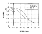
その際、各発光部16R,16G,16Bが図2に示したような共振器構造であるため、各発光部16R,16G,16Bから発せられた光は、例えば図6に示したように、角度依存の配光特性を示すことになる。これにより、輝度の視野角依存性が大きくなるため、そのままではこの場合、例えば視野角が45°のときの輝度が、正面輝度(視野角が0°のときの輝度)の40%程度に低下してしまうことになる。
At this time, since each
ここで、例えば図7(A),(B)に示した比較例1に係る従来の有機EL表示装置では、上記した角度依存の配光特性による輝度の視野角依存性を抑えるため、拡散板108が設けられている。この拡散板108では、低屈折率領域108L内に、真球状のビーズをなす高屈折率領域108Hがランダムに配置されている。このような拡散板108では、面光源106から入射光は、図7(A)に示したZ−X断面内(厚み方向)および図7(B)に示したX−Y平面内のいずれの方向においても、図中の光線L101,L102のように、屈折率差によるレンズ効果を多重に受けるため、散乱されることになる。これにより、その散乱作用に起因して、表示画像のぼけやにじみおよび輝度低下が生じるため、表示画質が劣化してしまうことになる。
Here, for example, in the conventional organic EL display device according to Comparative Example 1 shown in FIGS. 7A and 7B, in order to suppress the viewing angle dependency of luminance due to the above-described angle-dependent light distribution characteristic, a diffusion plate is used. 108 is provided. In the
一方、例えば図8(A),(B)に示した比較例2に係る従来の有機EL表示装置では、上記した角度依存の配光特性による輝度の視野角依存性を抑えるため、異方性散乱フィルム208が設けられている。この異方性散乱フィルム208では、図8(B)に示したように、フィルムの面内方向(X−Y平面内の方向)に、低屈折率領域208Lと高屈折率領域208Hとが形成されている。また、この高屈折率領域208Hは、低屈折率領域20L内でマトリクス状に配置されると共に、例えば図8(A)に示したように、厚み方向(Z方向)に対して傾斜角α201をなす円柱状となっている。このような異方性散乱フィルム208では、面内方向の屈折率差により、高屈折率領域208内での多重の全反射による散乱作用(図中の光線L201参照)と、透過作用(図中の光線L202参照)とが生じ、角度選択性を示す。すなわち、比較例1に係る拡散板108と同様の多重反射による散乱作用に加え、フィルム面内方向の円柱形状の高屈折率領域208Hにおけるレンズ効果によって、新たな散乱作用が生じている。しかしながら、このような異方性散乱フィルム208においても、比較例1に係る拡散板108と同様に、フィルム面内方向において、拡散作用に起因した強い画素ぼかしの効果および輝度低下が生じるため(図中の光線L202参照)、やはり表示画質が劣化してしまうことになる。
On the other hand, in the conventional organic EL display device according to Comparative Example 2 shown in FIGS. 8A and 8B, for example, anisotropy is used to suppress the viewing angle dependency of luminance due to the angle-dependent light distribution characteristic. A
そこで本実施の形態の有機EL表示装置1では、例えば図4(A),(B)に示した散乱層181〜183からなる異方性散乱フィルム18が設けられている。具体的には、この異方性散乱フィルム18では、フィルム面内方向(X−Y平面内の方向)の領域が、厚み方向(Z方向)から傾斜した四角柱状からなる複数の高屈折率領域18Hと、低屈折率領域18Lとから構成され、これにより入射光の入射方向に応じて異なる作用がなされる。すなわち、四角柱状の高屈折率領域18Hの傾斜方向からの入射光(例えば、図中の光線L1)は、この高屈折率領域18H内で多重反射され、傾斜方向へ選択的に散乱された表示光となる。また、この傾斜方向以外の方向からの入射光(例えば、図中の光線L2)は、高屈折率領域18Hを通過して表示光となる。その際、高屈折率領域18Hが四角柱形状であると共にその矩形断面の一辺(ここでは、X方向の一辺)が面光源160の発光面と略平行となっているため、比較例1に係る拡散板108(高屈折率領域108Hがおよび比較例2に係る異方性散乱フィルム208(高屈折率領域208Hが円柱状)とは異なり、傾斜方向以外の方向からの入射光(例えば、図中の光線L2)が高屈折率領域18Hにおいて散乱されず、入射角(例えば、図中の入射角θ)を維持したまま出射される。すなわち、ビーズや円柱の断面のように曲面を通過しないことから、フィルム面内方向においてレンズ効果が発生せず、入射光の入射角θが維持されるため、表示画像においてぼけが生じないと共に、輝度低下も抑えられる。
Therefore, in the organic
なお、このような効果は、上記したように、四角柱状の高屈折率領域18Hにおける矩形断面の一辺が、面光源160の発光面と略平行となっている場合に生ずるものである。したがって、例えば図9に示した異方性散乱フィルム308のように、四角柱状の高屈折率領域18Hにおける矩形断面の一辺が、面光源160の発光面に対して傾斜している場合には、比較例1,2と同様に、フィルム面内方向(X−Y平面内の方向)においてレンズ効果が発生してしまうことになる(図中の光線L301,L302参照)。
In addition, as described above, such an effect occurs when one side of the rectangular cross section in the quadrangular columnar high
ここで、図10(A),(B)は、図3に示した各散乱層181〜183を、単層構造で有機EL表示装置1に設けた場合における配光特性例を表したものである。これらの図において、「±15」,「05−35」,「15−45」,「25−55」はそれぞれ、散乱層における傾斜角αの範囲を表しており、以下同様である。図10(B)に示した相対輝度の視野各依存性によれば、四角柱状の高屈折率領域18Hの傾斜角αの大きさに応じて、各散乱層181〜183を設けない場合(有機EL素子本来の配光特性)と比べ、相対輝度が向上している角度領域が存在していることが分かる。このことは、例えば図5に示したようなヘイズ特性の散乱層を用いることにより、輝度の視野角特性の向上が可能であることを示している。また、図10(A)に示した絶対輝度の視野各依存性によれば、正面輝度の低下は例えば9%程度であり、従来の拡散板や散乱板(比較例1)を用いたとき(正面輝度の低下が約50%程度)と比べ、大幅に抑制されていることが分かる。
Here, FIGS. 10A and 10B show examples of light distribution characteristics when the scattering layers 181 to 183 shown in FIG. 3 are provided in the organic
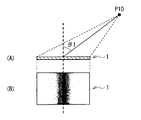
ただし、このとき例えば図11中の符号P1で示したように、フィルムの厚み方向の散乱に起因して、輝度の視野角特性が改善している角度領域の低角側に、輝度の視野角特性が劣化している角度領域(凹部)が存在していることが分かる。このような凹部が生じていると、例えば図12(A),(B)に示したように、表示エリアの画角(例えば、観察者が地点P10にいる場合の画角θ1)によって、観察面に暗帯が発生してしまうことを意味している。このような暗帯が発生すると、表示画質において重大な欠陥となってしまう。 However, at this time, for example, as indicated by reference numeral P1 in FIG. 11, the luminance viewing angle is on the lower angle side of the angle region where the luminance viewing angle characteristics are improved due to scattering in the thickness direction of the film. It can be seen that there is an angular region (concave portion) where the characteristics are degraded. When such a concave portion is generated, as shown in FIGS. 12A and 12B, for example, an observation is performed depending on the angle of view of the display area (for example, the angle of view θ1 when the observer is at the point P10). This means that a dark band occurs on the surface. When such a dark band occurs, it becomes a serious defect in display image quality.
そこで、本実施の形態の有機EL表示装置1では、例えば図13に示したように、配光特性G11を示す散乱層における凹部P11に対して、それよりも低角で散乱する散乱層(例えば、図中の配光特性G12を示すもの)の凸部P12を重ねることにより、散乱層の凹部P11を解消させるようにするのが好ましい。このようにして、複数の散乱層を積層させて組み合わせる(具体的には、各散乱層における傾斜角αが、面光源160の発光面側から有機EL表示装置1の観察面側となるのに従って、低角→中間角→高角のように、次第に大きくなるように設定する)ことにより、各散乱層における輝度の視野角特性での凹凸を相殺もしくは緩和させることが可能となるからである。
Therefore, in the organic
具体的には、例えば表1に示した傾斜角α、凸部の角度(凸角度)、凹部の角度(凹角度)および層数からなる各散乱層では、例えば図14に示したような配光特性G21〜G23を示す。また、各散乱層を低角側から積層させた場合には、例えば図15(A),(B)に示したような輝度の視野角特性を示すようになる。これらの図において、「(±25)&(05−35)*2&(15−45)*2」は、傾斜角α=±25程度の散乱層と、傾斜角α=5°〜35°程度の散乱層2層と、傾斜角α=15°〜45°程度の散乱層2層とを積層させたものを表している。具体的には、積層時の輝度の凹凸に若干のずれがあるために滑らかな変化とはなっていないが、各散乱層単体で発生していた凹凸がほぼ解消され、暗帯も観察されなかった。また、図15(A)に示した絶対輝度の視野角依存性によれば、散乱層の多層化によって、各散乱層単体のときよりも正面輝度の低下が約12%増加してしまっているものの、従来の拡散板等を用いたとき(正面輝度の低下が約50%)と比べると、正面輝度の低下は低く抑えられていることが分かる。また、図15(B)に示した相対輝度の視野角依存性によれば、異方性散乱フィルム18を設けない場合と比べ、視野角45°のときの輝度が約30%向上していることが分かる。さらに、例えば図16に示した色度ずれの視野角依存性によれば、異方性散乱フィルム18を設けない場合と比べ、異方性散乱フィルム18による散乱作用により、色度のずれ量が約1/4程度に減少していることが分かる。
Specifically, for example, in each scattering layer including the inclination angle α, the convex portion angle (convex angle), the concave portion angle (concave angle), and the number of layers shown in Table 1, the arrangement as shown in FIG. The optical characteristics G21-G23 are shown. Further, when the scattering layers are laminated from the low angle side, for example, the viewing angle characteristics of luminance as shown in FIGS. 15A and 15B are exhibited. In these figures, “(± 25) & (05-35) * 2 & (15-45) * 2” means a scattering layer having an inclination angle α = about ± 25 and an inclination angle α = about 5 ° to 35 °. And two scattering layers having an inclination angle α of about 15 ° to 45 ° are stacked. Specifically, although there is a slight deviation in the unevenness of brightness at the time of lamination, it does not change smoothly, but the unevenness that occurred in each scattering layer alone is almost eliminated, and dark bands are not observed It was. Further, according to the viewing angle dependency of the absolute luminance shown in FIG. 15A, the decrease in front luminance is increased by about 12% as compared with the case of each scattering layer alone due to the multilayered scattering layer. However, it can be seen that the decrease in front luminance is suppressed to a lower level than when a conventional diffusion plate or the like is used (the decrease in front luminance is about 50%). Further, according to the viewing angle dependency of the relative luminance shown in FIG. 15B, the luminance at a viewing angle of 45 ° is improved by about 30% compared to the case where the

以上のように本実施の形態では、異方性散乱フィルム18において、面内方向(X−Y平面内の方向)の領域を、厚み方向(Z方向)から傾斜した四角柱状からなる複数の高屈折率領域18Hと、低屈折率領域18Lとから構成するようにしたので、四角柱状の高屈折率領域18Hの傾斜方向に応じて、散乱された表示光を選択的に出射させることができる。また、四角柱状の高屈折率領域18Hにおける矩形断面の一辺(X方向の一辺)が面光源160の発光面と略平行となるようにしたので、傾斜方向以外の方向からの入射光が散乱されずに入射角θを維持したまま出射することができ、従来と比べ、入射光の光量損失を低減する共に、散乱に起因した表示画像のぼけを抑えることができる。よって、正面方向の輝度低下の抑制と視野角特性(輝度および色度ずれの視野角特性)の向上とを両立させつつ、従来よりも表示画質を向上させることが可能となる。
As described above, in the present embodiment, in the
また、正面方向の輝度低下を抑制することができるため、有機EL表示装置1の低消費電力化および電流密度上昇の抑制が可能となり、有機EL素子等の劣化を抑え、長寿命化を図ることが可能となる。
Moreover, since the brightness | luminance fall of a front direction can be suppressed, it becomes possible to reduce the power consumption of the organic
また、異方性散乱フィルム18を、積層された複数の散乱層181〜183により構成すると共に、四角柱状の高屈折率領域18Hにおける傾斜角αが散乱層ごとに互いに異なっている(具体的には、四角柱状の高屈折率領域18Hにおける傾斜角αが、発光面側から観察面側となるのに従って次第に大きくなっている)ようにしたので、各散乱層における輝度の視野角特性での凹凸を、相殺もしくは緩和させることが可能となる。
In addition, the
以下、本発明の変形例をいくつか挙げて説明する。なお、上記実施の形態における構成要素と同一のものには同一の符号を付し、適宜説明を省略する。 Hereinafter, some modified examples of the present invention will be described. In addition, the same code | symbol is attached | subjected to the same thing as the component in the said embodiment, and description is abbreviate | omitted suitably.
[変形例1]
図17(A),(B)は、変形例1に係る異方性散乱層(異方性散乱フィルム18A)の断面構成を表したものである。この異方性散乱フィルム18Aは、上記実施の形態で説明した視野角改善手法を、表示装置の長手方向(X方向)だけではなく垂直方向(Y方向)に対しても適用させたものであり、4層×3=12層の構造となっている。具体的には、低角散乱層181A〜181Dでは、傾斜角αが低角となり、中間散乱層182A〜182Dでは、傾斜角αが中間角となり、高角散乱層183A〜183Dでは、傾斜角αが高角となっている。また、低角散乱層181A、中間散乱層182Aおよび高角散乱層183Aにおける傾斜方向は、例えば図17(B)中の矢印Paの方向(+X方向)となっており、低角散乱層181B、中間散乱層182Bおよび高角散乱層183Bにおける傾斜方向は、例えば図17(B)中の矢印Pbの方向(−X方向)となっており、低角散乱層181C、中間散乱層182Cおよび高角散乱層183Cにおける傾斜方向は、例えば図17(B)中の矢印Pcの方向(+Y方向)となっており、低角散乱層181D、中間散乱層182Dおよび高角散乱層183Dにおける傾斜方向は、例えば図17(B)中の矢印Pdの方向(−Y方向)となっている。さらに、このような傾斜角αは、面光源160の発光面側から有機EL表示装置1の観察面側となるのに従って、低角→中間角→高角のように、次第に大きくなるように設定されている。
[Modification 1]
17A and 17B show a cross-sectional configuration of an anisotropic scattering layer (
このようにして本変形例の異方性散乱フィルム18Aでは、上記実施の形態で説明した視野角改善手法を、表示装置の長手方向(X方向)だけではなく垂直方向(Y方向)に対しても適用させるようにしたので、上下左右方向(+X方向、−X方向、+Y方向および−Y方向)に対して、視野角改善を行うことが可能となる。
Thus, in the
[変形例2]
図18は、変形例2に係る異方性散乱層(異方性散乱フィルム18B)の断面構成を表したものである。この異方性散乱フィルム18Bでは、積層構造を保持している支持部が、AR(反射防止)処理が施されたAR支持部180Bとなっている。
[Modification 2]
FIG. 18 illustrates a cross-sectional configuration of an anisotropic scattering layer (
このようにして本変形例の異方性散乱フィルム18Bでは、異方性散乱フィルム18Bにおける支持部としてAR支持部180Bを用いるようにしたので、ARフィルムを別途用意する必要がなくなる。よって、表面からの正反射および追加のAR処理を不要とすることにより、コストを低減することが可能となる。
Thus, in the
[変形例3]
図19は、変形例3に係る表示装置(有機EL表示装置1C)の断面構成を表したものである。この有機EL表示装置1Cでは、異方性散乱フィルム18Cが、発光面の近傍、具体的には保護層13と封止層14との層間に配置されている。
[Modification 3]
FIG. 19 illustrates a cross-sectional configuration of a display device (organic EL display device 1C) according to
このようにして本変形例の有機EL表示装置1Cでは、異方性散乱フィルム18Cを発光面の近傍に配置するようにしたので、異方性散乱フィルム18Cが多層構造の場合であっても、表示画像のぼけを最小限に抑えることが可能となる。 In this way, in the organic EL display device 1C of the present modification, the anisotropic scattering film 18C is arranged in the vicinity of the light emitting surface, so even if the anisotropic scattering film 18C has a multilayer structure, It is possible to minimize blurring of the display image.
[変形例4]
図20は、変形例4に係る表示装置(有機EL表示装置1D)の断面構成を表したものである。この有機EL表示装置1Dでは、各発光部16R,16G,16B(有機EL素子)の観察面側に、光取り出し効率を向上させるための反射鏡19が設けられている。そしてこのような反射鏡19によって、各発光部16R,16G,16Bから異方性散乱フィルム18への入射光が、角度依存の配光特性を示すようになっている。
[Modification 4]
FIG. 20 illustrates a cross-sectional configuration of a display device (organic EL display device 1D) according to Modification 4. In the organic EL display device 1D, a reflecting mirror 19 for improving light extraction efficiency is provided on the observation surface side of each
このようにして本変形例の有機EL表示装置1Dでは、各発光部16R,16G,16B(有機EL素子)の観察面側に、光取り出し効率を向上させるための反射鏡19と、異方性散乱フィルム18とを設けるようにしたので、上記実施の形態と同様の作用により同様の効果を得ることが可能となる。
As described above, in the organic EL display device 1D of the present modification, the reflecting mirror 19 for improving the light extraction efficiency and the anisotropy are provided on the observation surface side of each
[変形例5]
図21は、変形例5に係る表示装置(液晶表示装置2)の断面構成を表したものである。本変形例は、これまで説明した有機EL表示装置の代わりに、液晶表示装置において異方性散乱フィルムを設けるようにしたものである。この液晶表示装置2では、発光素子が、バックライト20と、液晶素子とを含んで構成されている。
[Modification 5]
FIG. 21 illustrates a cross-sectional configuration of a display device (liquid crystal display device 2) according to Modification 5. In this modification, an anisotropic scattering film is provided in a liquid crystal display device instead of the organic EL display device described so far. In the liquid
また、この液晶素子は、一対の透明基板(駆動用基板11および対向基板15)と、これら一対の透明基板間に充填された液晶層22と、透明基板上に配置された一対の偏光板211,212と、駆動用基板11側の画素電極261と、対向電極15側の対向電極262とを含んで構成されている。そして異方性散乱フィルム18が、観察面側の偏光板212よりも観察面側に配置されている。ただし、この異方性散乱フィルム18の配置位置は、この位置には限られない。
The liquid crystal element includes a pair of transparent substrates (the driving
このようにして本変形例の液晶表示装置2では、液晶表示装置2において異方性散乱フィルム18を設けるようにしたので、上記実施の形態と同様の作用により同様の効果を得ることが可能となる。
Thus, in the liquid
また、異方性散乱フィルム18を、観察面側の偏光板212よりも観察面側に配置するようにしたので、発光面側に配置した場合と比べ、コントラストの低下を抑えることが可能となる。
Further, since the
(適用例)
次に、図22〜図26を参照して、上記実施の形態および変形例で説明した表示装置の適用例について説明する。上記実施の形態等の表示装置は、テレビジョン装置,デジタルカメラ,ノート型パーソナルコンピュータ、携帯電話等の携帯端末装置あるいはビデオカメラなど、外部から入力された映像信号あるいは内部で生成した映像信号を、画像あるいは映像として表示するあらゆる分野の電子機器に適用することが可能である。
(Application example)
Next, with reference to FIGS. 22 to 26, application examples of the display device described in the above embodiment and modifications will be described. A display device such as the above embodiment is a television device, a digital camera, a notebook personal computer, a mobile terminal device such as a mobile phone, or a video camera, such as an externally input video signal or an internally generated video signal. The present invention can be applied to electronic devices in various fields that display images or videos.
(適用例1)
図22は、上記実施の形態等の表示装置が適用されるテレビジョン装置の外観を表したものである。このテレビジョン装置は、例えば、フロントパネル511およびフィルターガラス512を含む映像表示画面部510を有しており、この映像表示画面部510は、上記実施の形態等に係る表示装置により構成されている。
(Application example 1)
FIG. 22 illustrates an appearance of a television device to which the display device of the above-described embodiment or the like is applied. This television apparatus has, for example, a video display screen unit 510 including a front panel 511 and a filter glass 512, and the video display screen unit 510 is configured by the display device according to the above-described embodiment and the like. .
(適用例2)
図23は、上記実施の形態等の表示装置が適用されるデジタルカメラの外観を表したものである。このデジタルカメラは、例えば、フラッシュ用の発光部521、表示部522、メニュースイッチ523およびシャッターボタン524を有しており、その表示部522は、上記実施の形態等に係る表示装置により構成されている。
(Application example 2)
FIG. 23 shows the appearance of a digital camera to which the display device of the above-described embodiment or the like is applied. The digital camera includes, for example, a flash light emitting unit 521, a display unit 522, a menu switch 523, and a
(適用例3)
図24は、上記実施の形態等の表示装置が適用されるノート型パーソナルコンピュータの外観を表したものである。このノート型パーソナルコンピュータは、例えば、本体531,文字等の入力操作のためのキーボード532および画像を表示する表示部533を有しており、その表示部533は、上記実施の形態等に係る表示装置により構成されている。
(Application example 3)
FIG. 24 illustrates an appearance of a notebook personal computer to which the display device of the above-described embodiment or the like is applied. This notebook personal computer has, for example, a main body 531, a keyboard 532 for inputting characters and the like, and a display unit 533 for displaying an image. The display unit 533 is a display according to the above-described embodiment and the like. It is comprised by the apparatus.
(適用例4)
図25は、上記実施の形態等の表示装置が適用されるビデオカメラの外観を表したものである。このビデオカメラは、例えば、本体部541,この本体部541の前方側面に設けられた被写体撮影用のレンズ542,撮影時のスタート/ストップスイッチ543および表示部544を有しており、その表示部544は、上記実施の形態等に係る表示装置により構成されている。
(Application example 4)
FIG. 25 shows the appearance of a video camera to which the display device of the above-described embodiment or the like is applied. The video camera includes, for example, a main body 541, a
(適用例5)
図26は、上記実施の形態等の表示装置が適用される携帯電話機の外観を表したものである。この携帯電話機は、例えば、上側筐体710と下側筐体720とを連結部(ヒンジ部)730で連結したものであり、ディスプレイ740,サブディスプレイ750,ピクチャーライト760およびカメラ770を有している。そのディスプレイ740またはサブディスプレイ750は、上記実施の形態等に係る表示装置により構成されている。
(Application example 5)
FIG. 26 shows an appearance of a mobile phone to which the display device of the above-described embodiment or the like is applied. For example, this mobile phone is obtained by connecting an
以上、実施の形態、変形例および適用例を挙げて本発明を説明したが、本発明はこれらの実施の形態等に限定されるものではなく、種々の変形が可能である。 While the present invention has been described with reference to the embodiments, modifications, and application examples, the present invention is not limited to these embodiments and the like, and various modifications are possible.
例えば、上記実施の形態では、異方性散乱フィルムが、積層された複数の散乱層からなる多層構造により構成されている場合について説明したが、異方性散乱フィルムが単一の散乱層により構成されているようにしてもよい。また、この場合において、四角柱状の高屈折率領域18Hが、単一の散乱層内で互いに異なる複数の傾斜角αを有するようにしてもよい。
For example, in the above embodiment, the case where the anisotropic scattering film is configured by a multilayer structure including a plurality of stacked scattering layers has been described. However, the anisotropic scattering film is configured by a single scattering layer. You may be made to do. In this case, the quadrangular prism-shaped high
また、異方性散乱フィルムの配置位置は、上記実施の形態で説明した位置には限られず、発光素子の観察面側の任意の位置に配置することが可能である。 The arrangement position of the anisotropic scattering film is not limited to the position described in the above embodiment, and can be arranged at an arbitrary position on the observation surface side of the light emitting element.
また、上記実施の形態では、四角柱状の高屈折率領域18Hが、低屈折率領域18L内でマトリクス状に配置されている場合について説明したが、例えば、四角柱状の高屈折率領域18Hが、低屈折率領域18L内でランダムに配置されているようにしてもよい。
In the above-described embodiment, the case where the rectangular columnar high
また、異方性散乱フィルムの各散乱層における高屈折率領域18Hの傾斜方向および層数は、上記実施の形態で説明したものには限られず、任意の傾斜方向および層数に設定することが可能である。例えば、120度ずつ異なる傾斜方向の3層構造×3種類の散乱角=9層の構造としてもよい。
Further, the inclination direction and the number of layers of the high
また、上記実施の形態では、発光素子を備えた表示装置の一例として、有機EL素子を発光部16R,16G,16Bにおいて備えた有機EL表示装置1,1C,1Dと、液晶素子を備えた液晶表示装置2とを挙げて説明したが、本発明は、例えば、発光素子として無機EL素子を備えた無機EL表示装置や、FED(Field Emission Display;電界放出ディスプレイ)などの他の表示装置にも適用することが可能である。
Moreover, in the said embodiment, as an example of the display apparatus provided with the light emitting element, the organic
1,1A〜1D…有機EL表示装置、10R,10G,10B…画素、11…駆動用基板、12…絶縁層、12−1…開口部、13…保護層、14…封止層、15…対向基板、16R,16G,16B…発光部、160…面光源、161…第1電極、162…正孔注入層、163…正孔輸送層、164…発光層、165…電子輸送層、166…第2電極、17R,17G,17B…カラーフィルタ層、18,18A〜18C…異方性散乱フィルム、18L…低屈折率領域、18H…高屈折率層(四角柱状硬化領域)、180…支持部、180B…AR支持部、181A〜181D…低角散乱層、182A〜182D…中間散乱層、183A〜183D…高角散乱層、19…反射鏡、2…液晶表示装置、211,212…偏光板、22…液晶層、261,262…画素電極、510…映像表示画面部、511…フロントパネル、512…フィルターガラス、521…発光部、522…表示部、523…メニュースイッチ、524…シャッターボタン、531…本体、532…キーボード、533…表示部、541…本体部、542…レンズ、543…スタート/ストップスイッチ、544…表示部、710…上部筐体、720…下部筐体、730…連結部、740…ディスプレイ、750…サブディスプレイ、760…ピクチャーライト、770…カメラ、BM…ブラックマトリクス層、α…傾斜角、θ…入射角(射出角)、L1〜L2…光線、Lout…表示光(射出光)。
DESCRIPTION OF
Claims (13)
前記発光素子の観察面側に配置され、角度依存の配光特性を有する前記発光素子からの入射光を散乱させるための異方性散乱層と
を備え、
前記異方性散乱層では、面内方向の領域が、複数の高屈折率領域と、これら高屈折率領域よりも屈折率の低い低屈折率領域とから構成され、
前記高屈折率領域が、厚み方向から傾斜してなる四角柱状であると共に、この四角柱状の高屈折率領域における矩形断面の一辺が、前記発光素子の発光面と略平行である
表示装置。 A light emitting device disposed in each pixel;
An anisotropic scattering layer disposed on the observation surface side of the light-emitting element and for scattering incident light from the light-emitting element having an angle-dependent light distribution characteristic;
In the anisotropic scattering layer, the in-plane direction region is composed of a plurality of high refractive index regions and a low refractive index region having a lower refractive index than these high refractive index regions,
The high refractive index region has a quadrangular prism shape inclined from the thickness direction, and one side of a rectangular cross section in the quadrangular columnar high refractive index region is substantially parallel to a light emitting surface of the light emitting element.
前記四角柱状の高屈折率領域が、前記単一の散乱層内で、互いに異なる複数の傾斜角を有する
請求項1に記載の表示装置。 The anisotropic scattering layer is constituted by a single scattering layer;
The display device according to claim 1, wherein the square columnar high refractive index region has a plurality of inclination angles different from each other in the single scattering layer.
前記四角柱状の高屈折率領域における傾斜角が、前記複数の散乱層ごとに互いに異なっている
請求項1に記載の表示装置。 The anisotropic scattering layer is composed of a plurality of stacked scattering layers,
The display device according to claim 1, wherein an inclination angle in the square columnar high refractive index region is different for each of the plurality of scattering layers.
請求項3に記載の表示装置。 The display device according to claim 3, wherein an inclination angle in the quadrangular columnar high refractive index region is set to gradually increase from the light emitting surface side to the observation surface side.
請求項1に記載の表示装置。 The display device according to claim 1, wherein an inclination angle in the square columnar high refractive index region is set to be equal to or less than a critical angle of the incident light.
請求項1に記載の表示装置。 The plurality of high refractive index regions are arranged in a matrix in the in-plane direction of the anisotropic scattering layer, and the low refractive index regions are arranged in gaps between the high refractive index regions. The display device described in 1.
請求項1に記載の表示装置。 The display device according to claim 1, wherein the anisotropic scattering layer is disposed in the vicinity of the light emitting surface.
請求項1ないし請求項7のいずれか1項に記載の表示装置。 The display device according to claim 1, wherein the light emitting element is an organic EL element, and is configured as an organic EL display device.
請求項8に記載の表示装置。 The display device according to claim 8, wherein the organic EL element has a resonator structure.
請求項8に記載の表示装置。 The display device according to claim 8, wherein a reflecting mirror is provided on the observation surface side of the organic EL element.
請求項1ないし請求項7のいずれか1項に記載の表示装置。 The display device according to claim 1, wherein the light emitting element includes a light source and a liquid crystal element, and is configured as a liquid crystal display device.
前記異方性散乱層が、前記一対の偏光板のうちの前記観察面側の偏光板よりも、観察面側に配置されている
請求項11に記載の表示装置。 The liquid crystal element includes a pair of transparent substrates, a liquid crystal layer filled between the pair of transparent substrates, and a pair of polarizing plates disposed on the transparent substrate,
The display device according to claim 11, wherein the anisotropic scattering layer is disposed closer to an observation surface than a polarizing plate on the observation surface side of the pair of polarizing plates.
前記表示装置は、
各画素に配置された発光素子と、
前記発光素子の観察面側に配置され、角度依存の配光特性を有する前記発光素子からの入射光を散乱させるための異方性散乱層と
を有し、
前記異方性散乱層では、面内方向の領域が、複数の高屈折率領域と、これら高屈折率領域よりも屈折率の低い低屈折率領域とから構成され、
前記高屈折率領域が、厚み方向から傾斜してなる四角柱状であると共に、この四角柱状の高屈折率領域における矩形断面の一辺が、前記発光素子の発光面と略平行である
電子機器。 A display device having a display function;
The display device
A light emitting device disposed in each pixel;
An anisotropic scattering layer for scattering incident light from the light emitting element, which is disposed on the observation surface side of the light emitting element and has an angle-dependent light distribution characteristic;
In the anisotropic scattering layer, the in-plane direction region is composed of a plurality of high refractive index regions and a low refractive index region having a lower refractive index than these high refractive index regions,
The electronic device, wherein the high refractive index region has a quadrangular prism shape inclined from a thickness direction, and one side of a rectangular cross section in the quadrangular columnar high refractive index region is substantially parallel to the light emitting surface of the light emitting element.
Priority Applications (1)
| Application Number | Priority Date | Filing Date | Title |
|---|---|---|---|
| JP2008115769A JP2009265406A (en) | 2008-04-25 | 2008-04-25 | Display device and electronic appliance |
Applications Claiming Priority (1)
| Application Number | Priority Date | Filing Date | Title |
|---|---|---|---|
| JP2008115769A JP2009265406A (en) | 2008-04-25 | 2008-04-25 | Display device and electronic appliance |
Publications (1)
| Publication Number | Publication Date |
|---|---|
| JP2009265406A true JP2009265406A (en) | 2009-11-12 |
Family
ID=41391326
Family Applications (1)
| Application Number | Title | Priority Date | Filing Date |
|---|---|---|---|
| JP2008115769A Pending JP2009265406A (en) | 2008-04-25 | 2008-04-25 | Display device and electronic appliance |
Country Status (1)
| Country | Link |
|---|---|
| JP (1) | JP2009265406A (en) |
Cited By (10)
| Publication number | Priority date | Publication date | Assignee | Title |
|---|---|---|---|---|
| EP2325528A1 (en) | 2009-11-20 | 2011-05-25 | JATCO Ltd | Control apparatus for automatic transmission |
| JP2013114187A (en) * | 2011-11-30 | 2013-06-10 | National Institute Of Advanced Industrial & Technology | Manufacturing method of light scattering element, and light scattering element recording medium |
| JP2013134907A (en) * | 2011-12-27 | 2013-07-08 | Nippon Zeon Co Ltd | Organic electroluminescence display device |
| JP2013195672A (en) * | 2012-03-19 | 2013-09-30 | Tomoegawa Paper Co Ltd | Anisotropic optical film |
| WO2014084361A1 (en) * | 2012-11-29 | 2014-06-05 | 株式会社巴川製紙所 | Anisotropic optical film |
| JP2014132525A (en) * | 2013-01-04 | 2014-07-17 | Japan Display Inc | Organic EL display device |
| JP2015099804A (en) * | 2015-03-03 | 2015-05-28 | コニカミノルタ株式会社 | Organic electroluminescent element and luminaire |
| WO2018159470A1 (en) * | 2017-03-02 | 2018-09-07 | シャープ株式会社 | Display apparatus and head mount display |
| CN111724697A (en) * | 2020-05-18 | 2020-09-29 | 明基材料有限公司 | Electroluminescent display device |
| CN112088578A (en) * | 2018-05-14 | 2020-12-15 | 株式会社巴川制纸所 | Head-mounted display |
Citations (5)
| Publication number | Priority date | Publication date | Assignee | Title |
|---|---|---|---|---|
| JP2002189105A (en) * | 2000-12-21 | 2002-07-05 | Toppan Printing Co Ltd | Off-axis anisotropic light scattering film and display device using the same |
| JP2004164912A (en) * | 2002-11-11 | 2004-06-10 | Seiko Epson Corp | Display body, display panel and display device |
| JP2006003506A (en) * | 2004-06-16 | 2006-01-05 | Toppan Printing Co Ltd | Diffusion film, polarizing element, and liquid crystal display element |
| JP2006138938A (en) * | 2004-11-10 | 2006-06-01 | Seiko Instruments Inc | Screen and image projecting system using the same |
| JP2007305508A (en) * | 2006-05-15 | 2007-11-22 | Sony Corp | Light-emitting device, and light control film |
-
2008
- 2008-04-25 JP JP2008115769A patent/JP2009265406A/en active Pending
Patent Citations (5)
| Publication number | Priority date | Publication date | Assignee | Title |
|---|---|---|---|---|
| JP2002189105A (en) * | 2000-12-21 | 2002-07-05 | Toppan Printing Co Ltd | Off-axis anisotropic light scattering film and display device using the same |
| JP2004164912A (en) * | 2002-11-11 | 2004-06-10 | Seiko Epson Corp | Display body, display panel and display device |
| JP2006003506A (en) * | 2004-06-16 | 2006-01-05 | Toppan Printing Co Ltd | Diffusion film, polarizing element, and liquid crystal display element |
| JP2006138938A (en) * | 2004-11-10 | 2006-06-01 | Seiko Instruments Inc | Screen and image projecting system using the same |
| JP2007305508A (en) * | 2006-05-15 | 2007-11-22 | Sony Corp | Light-emitting device, and light control film |
Cited By (14)
| Publication number | Priority date | Publication date | Assignee | Title |
|---|---|---|---|---|
| EP2325528A1 (en) | 2009-11-20 | 2011-05-25 | JATCO Ltd | Control apparatus for automatic transmission |
| JP2013114187A (en) * | 2011-11-30 | 2013-06-10 | National Institute Of Advanced Industrial & Technology | Manufacturing method of light scattering element, and light scattering element recording medium |
| JP2013134907A (en) * | 2011-12-27 | 2013-07-08 | Nippon Zeon Co Ltd | Organic electroluminescence display device |
| JP2013195672A (en) * | 2012-03-19 | 2013-09-30 | Tomoegawa Paper Co Ltd | Anisotropic optical film |
| JP5670601B2 (en) * | 2012-11-29 | 2015-02-18 | 株式会社巴川製紙所 | Anisotropic optical film |
| WO2014084361A1 (en) * | 2012-11-29 | 2014-06-05 | 株式会社巴川製紙所 | Anisotropic optical film |
| JPWO2014084361A1 (en) * | 2012-11-29 | 2017-01-05 | 株式会社巴川製紙所 | Anisotropic optical film |
| US9958580B2 (en) | 2012-11-29 | 2018-05-01 | Tomoegawa Co., Ltd. | Anisotropic optical film |
| JP2014132525A (en) * | 2013-01-04 | 2014-07-17 | Japan Display Inc | Organic EL display device |
| JP2015099804A (en) * | 2015-03-03 | 2015-05-28 | コニカミノルタ株式会社 | Organic electroluminescent element and luminaire |
| WO2018159470A1 (en) * | 2017-03-02 | 2018-09-07 | シャープ株式会社 | Display apparatus and head mount display |
| US11073692B2 (en) | 2017-03-02 | 2021-07-27 | Sharp Kabushiki Kaisha | Display apparatus and head mount display |
| CN112088578A (en) * | 2018-05-14 | 2020-12-15 | 株式会社巴川制纸所 | Head-mounted display |
| CN111724697A (en) * | 2020-05-18 | 2020-09-29 | 明基材料有限公司 | Electroluminescent display device |
Similar Documents
| Publication | Publication Date | Title |
|---|---|---|
| JP2009265406A (en) | Display device and electronic appliance | |
| US10031265B2 (en) | Display device with a window including a light-path changing layer | |
| US20210234134A1 (en) | Anti-peeping display panel and anti-peeping display apparatus | |
| JP4715906B2 (en) | Display device | |
| JP5876027B2 (en) | Optical film and organic light emitting display device including the same | |
| KR102240334B1 (en) | Anisotropic optical film | |
| US8080939B2 (en) | Reflection plate, light-emitting device and method of manufacturing reflection plate | |
| TWI344801B (en) | Organic electroluminescent device, method of manufacturing organic electroluminescent device, and electronic apparatus | |
| CN113764602A (en) | Display device | |
| JP2006294491A (en) | Electroluminescence device, method for manufacturing the same, and electronic apparatus | |
| JP2007311046A (en) | Light-emitting device, method of manufacturing light-emitting device, and electronic equipment | |
| JP5470689B2 (en) | Display device | |
| EP2485567A1 (en) | Organic electroluminescence display apparatus | |
| EP3618119B1 (en) | Display device | |
| JP2007188708A (en) | Substrate for display element | |
| US20210098536A1 (en) | Light-emitting device, display apparatus, and image pickup apparatus | |
| US10168569B2 (en) | Display device, adhesive-layer-including light-diffusion member, and method of manufacturing the light-diffusion member | |
| WO2009098793A1 (en) | Organic el display and manufacturing method thereof | |
| JP2015176132A (en) | Optical sheet, organic electroluminescence light-emitting unit, and display device | |
| JP2011054424A (en) | Top-emission type organic el display and method of manufacturing the same, and color filter used for it | |
| CN216488149U (en) | Display device | |
| JP5787205B2 (en) | Color filter and organic EL display device | |
| JP2007109575A (en) | Substrate for electroluminescent element | |
| JP2007220431A (en) | Multi-color luminescent device and its manufacturing method | |
| JP4826939B2 (en) | Color conversion filter and color conversion light emitting device using the same |
Legal Events
| Date | Code | Title | Description |
|---|---|---|---|
| A621 | Written request for application examination |
Free format text: JAPANESE INTERMEDIATE CODE: A621 Effective date: 20110225 |
|
| A977 | Report on retrieval |
Free format text: JAPANESE INTERMEDIATE CODE: A971007 Effective date: 20120705 |
|
| A131 | Notification of reasons for refusal |
Free format text: JAPANESE INTERMEDIATE CODE: A131 Effective date: 20120717 |
|
| A02 | Decision of refusal |
Free format text: JAPANESE INTERMEDIATE CODE: A02 Effective date: 20121107 |