JP2009263785A - Connecting component metal material and method of manufacturing the same - Google Patents
Connecting component metal material and method of manufacturing the same Download PDFInfo
- Publication number
- JP2009263785A JP2009263785A JP2009087559A JP2009087559A JP2009263785A JP 2009263785 A JP2009263785 A JP 2009263785A JP 2009087559 A JP2009087559 A JP 2009087559A JP 2009087559 A JP2009087559 A JP 2009087559A JP 2009263785 A JP2009263785 A JP 2009263785A
- Authority
- JP
- Japan
- Prior art keywords
- copper
- tin
- thickness
- metal material
- base material
- Prior art date
- Legal status (The legal status is an assumption and is not a legal conclusion. Google has not performed a legal analysis and makes no representation as to the accuracy of the status listed.)
- Granted
Links
Images


Abstract
Description
本発明は、接続部品用金属材料およびその製造方法に関する。 The present invention relates to a metal material for connecting parts and a method for producing the same.
銅(Cu)、銅合金などの導電体の母材(以下、適宜、母材と記す。)上にスズ(Sn)、スズ合金などのめっき層を設けためっき材料は、母材の優れた導電性と強度、およびめっき層の優れた電気接続性と耐食性とはんだ付け性を備えた高性能導体材料として知られており、各種の端子やコネクタなどに広く用いられている。 A plating material in which a plating layer such as tin (Sn) or tin alloy is provided on a base material of a conductor such as copper (Cu) or a copper alloy (hereinafter referred to as a base material as appropriate) is excellent in the base material. It is known as a high-performance conductor material having electrical conductivity and strength, and excellent electrical connectivity, corrosion resistance, and solderability of the plated layer, and is widely used for various terminals and connectors.
ところで近年、電子制御化が進む中で嵌合型コネクタが多極化したため、オス端子群とメス端子群を挿抜する際に多大な力が必要になり、特に、自動車のエンジンルーム内などの狭い空間では挿抜作業が困難なため前記挿抜力の低減が強く求められている。 By the way, in recent years, with the progress of electronic control, the mating connector has become multipolar, so a great deal of force is required when inserting and removing the male terminal group and the female terminal group, especially in a narrow space such as in the engine room of an automobile. Since insertion / extraction work is difficult, reduction of the insertion / extraction force is strongly demanded.
前記挿抜力を低減する方法として、コネクタ端子表面のSnめっき層を薄くして端子間の接触圧力を弱める方法があるが、この方法はSnめっき層が軟質のため端子の接触面間にフレッティング現象が起きて端子間に導通不良が起きることがある。 As a method of reducing the insertion / extraction force, there is a method in which the Sn plating layer on the surface of the connector terminal is thinned to weaken the contact pressure between the terminals. This method is fretting between the contact surfaces of the terminals because the Sn plating layer is soft. A phenomenon may occur and poor conduction may occur between the terminals.
前記フレッティング現象とは、振動や温度変化などが原因で端子の接触面間に起きる微摺動により、端子表面の軟質のSnめっき層が摩耗し酸化して、比抵抗の大きい摩耗粉になる現象で、この現象が端子間に発生すると接続不良が起きる。そして、この現象は端子間の接触圧力が低いほど起き易い。 The fretting phenomenon is that the soft Sn plating layer on the surface of the terminal wears and oxidizes due to fine sliding that occurs between the contact surfaces of the terminal due to vibration, temperature change, etc., and becomes a wear powder having a large specific resistance. When this phenomenon occurs between terminals, a connection failure occurs. This phenomenon is more likely to occur as the contact pressure between the terminals is lower.
特許文献1には、Cu板条からなる母材の表面に、Cu−Sn合金被覆層とSn被覆層がこの順に形成されており、Cu−Sn合金被覆層の材料表面露出面積率が3〜75%、平均の厚さが0.1〜3.0μm、かつCu含有量が20〜70at%であり、前記Sn又はSn合金被覆層の平均の厚さが0.2〜5.0μmである接続部品用導電材料が記載されている。また、リフロー処理を行うことにより、Cu−Sn合金被覆層が形成されることも記載されている。
そして、この導電材料は、例えば自動車等において多極コネクタに使用した場合、オス、メス端子の嵌合時の挿入力が低く、組立作業を効率よく行うことができ、また高温雰囲気下で長時間保持されても、あるいは腐食環境下においても電気的信頼性(低接触抵抗)を維持できるとされている。
In
When this conductive material is used for a multipolar connector in an automobile or the like, for example, the insertion force when fitting the male and female terminals is low, the assembly work can be performed efficiently, and it can be performed for a long time in a high temperature atmosphere. It is said that electrical reliability (low contact resistance) can be maintained even when held or in a corrosive environment.
しかしながら、上記の接続部品用導電材料は、母材がCu板条からなるものであるが、母材が角線材である場合には、リフロー処理等の熱処理によるCu−Sn合金めっき線の製造では、リフロー処理後の表面性状が悪化する不具合が発生することがある。この不具合は、リフロー処理中に角線材上のSnが流れることでSnの分布が不均一になることが原因で発生すると考えられるが、前記特許文献1の技術では、母材がCu板条からなるため、母材が角線材である場合のような不具合は発生し得ない。
However, the conductive material for connecting parts described above is made of a Cu plate, but when the base material is a square wire, in the manufacture of a Cu-Sn alloy plated wire by heat treatment such as reflow treatment. In some cases, the surface properties after the reflow treatment deteriorate. This defect is considered to occur due to the non-uniform distribution of Sn due to the flow of Sn on the rectangular wire during the reflow process. However, in the technique of
そこで、本発明は、加熱処理後の表面性状が良好で、かつ後工程におけるはんだ付け性が良好な接続部品用金属材料およびその製造方法を提供することを目的とする。 Then, an object of this invention is to provide the metal material for connection components with the favorable surface property after heat processing, and the favorable solderability in a post process, and its manufacturing method.
上記課題は、以下の手段により達成される。すなわち、本発明は、
(1)銅または銅合金の角線材を母材とし、その最表面に実質的に銅およびスズで構成される銅スズ合金層が形成されている接続部品用金属材料において、前記最表面の銅スズ合金層は、さらに亜鉛、インジウム、アンチモン、ガリウム、鉛、ビスマス、カドミウム、マグネシウム、銀、金、アルミニウムの群から選ばれる少なくとも1種を、総量で前記スズの含有量に対する質量比で0.01%以上1%以下含有することを特徴とする接続部品用金属材料、
(2)前記母材上に、ニッケル、コバルト、鉄またはこれらの合金による層が形成されていることを特徴とする(1)項記載の接続部品用金属材料、
(3)銅または銅合金の角線材を母材とし、この母材上に亜鉛、インジウム、アンチモン、ガリウム、鉛、ビスマス、カドミウム、マグネシウム、銀、金、アルミニウムの群から選ばれる少なくとも1種を、総量で0.01質量%以上1質量%以下含有するスズ合金めっき層を形成して中間材料を得たのち、前記中間材料に加熱処理を行い、最表面に銅およびスズを含有する合金層を形成することを特徴とする接続部品用金属材料の製造方法、
(4)前記加熱処理前の前記スズ合金めっき層の厚さが0.3〜0.8μmであることを特徴とする(3)項記載の接続部品用金属材料の製造方法、
(5)前記母材と、前記スズ合金めっき層との間に、前記母材に近い側から、ニッケル、コバルト、鉄またはこれらの合金による層、銅めっき層または銅合金めっき層を設けて中間材料を得ることを特徴とする(3)項記載の接続部品用金属材料の製造方法、
(6)前記加熱処理前の前記スズめっき層またはスズ合金めっき層の厚さが0.3〜0.8μmであり、かつ前記銅めっき層の厚さ(Cu厚)に対する前記スズめっきまたはスズ合金めっき層の厚さ(Sn厚)の比(Sn厚/Cu厚)が2未満であることを特徴とする(5)項記載の接続部品用金属材料の製造方法、および
(7)前記加熱処理がリフロー処理であることを特徴とする、(3)〜(6)のいずれか1項に記載の接続部品用金属材料の製造方法
を提供するものである。
The above-mentioned subject is achieved by the following means. That is, the present invention
(1) In the metal material for connecting parts in which a copper or copper alloy square wire is used as a base material and a copper tin alloy layer substantially composed of copper and tin is formed on the outermost surface thereof, the outermost surface copper The tin alloy layer further includes at least one selected from the group consisting of zinc, indium, antimony, gallium, lead, bismuth, cadmium, magnesium, silver, gold, and aluminum in a mass ratio of 0.1 to a total content of tin. Metal material for connecting parts, characterized by containing from 01% to 1%,
(2) The metal material for connection parts as set forth in (1), wherein a layer made of nickel, cobalt, iron or an alloy thereof is formed on the base material.
(3) A copper or copper alloy square wire is used as a base material, and at least one selected from the group consisting of zinc, indium, antimony, gallium, lead, bismuth, cadmium, magnesium, silver, gold, and aluminum is provided on the base material. Then, after forming an intermediate material by forming a tin alloy plating layer containing 0.01% by mass or more and 1% by mass or less in a total amount, the intermediate material is subjected to heat treatment, and an alloy layer containing copper and tin on the outermost surface A method of manufacturing a metal material for connecting parts, characterized in that
(4) The method for producing a metal material for connection parts according to (3), wherein the thickness of the tin alloy plating layer before the heat treatment is 0.3 to 0.8 μm,
(5) Between the base material and the tin alloy plating layer, a layer made of nickel, cobalt, iron, or an alloy thereof, a copper plating layer or a copper alloy plating layer is provided between the base material and the side close to the base material. A method for producing a metal material for connecting parts as described in (3), wherein the material is obtained,
(6) The tin plating or tin alloy has a thickness of the tin plating layer or tin alloy plating layer before the heat treatment of 0.3 to 0.8 μm and the thickness (Cu thickness) of the copper plating layer The method for producing a metal material for connecting parts as described in (5), wherein the ratio (Sn thickness / Cu thickness) of the thickness (Sn thickness) of the plating layer is less than 2, and (7) the heat treatment The method for producing a metal material for connection parts as set forth in any one of (3) to (6), wherein is a reflow process.
本発明の接続部品用金属材料は、銅または銅合金の角線材(角棒材を含む)の母材の最表面に、実質的に銅およびスズで構成され、さらに亜鉛、インジウム、アンチモン、ガリウム、鉛、ビスマス、カドミウム、マグネシウム、銀、金、アルミニウムの群から選ばれる少なくとも1種を、総量で前記スズの含有量に対する質量比で0.01%以上1%以下含有するため、母材表面の凹凸に依存せず、加熱処理後の光沢を十分に有し、また、はんだ濡れ促進のための、予備はんだ性、後めっき性が極めて高い金属材料とすることができる。 The metal material for connecting parts of the present invention is substantially composed of copper and tin on the outermost surface of a base material of copper or a copper alloy square wire (including a square bar material), and further includes zinc, indium, antimony, and gallium. , Lead, bismuth, cadmium, magnesium, silver, gold, aluminum containing at least one selected from the group consisting of 0.01% and 1% by mass with respect to the content of tin. It is possible to obtain a metal material that has sufficient gloss after heat treatment and has extremely high pre-solderability and post-plating properties for promoting solder wetting.
本発明の接続部品用金属材料は、銅または銅合金により形成された角線材を母材とし、その最表面に実質的に銅およびスズで構成され、さらに亜鉛(Zn)、インジウム(In)、アンチモン(Sb)、ガリウム(Ga)、鉛(Pb)、ビスマス(Bi)、カドミウム(Cd)、マグネシウム(Mg)、銀(Ag)、金(Au)、アルミニウム(Al)の群から選ばれる少なくとも1種を、総量で前記スズの含有量に対する質量比で0.01%以上1%以下含有するものである。 The metal material for connecting parts according to the present invention is based on a square wire formed of copper or a copper alloy, and is substantially composed of copper and tin on the outermost surface thereof. Furthermore, zinc (Zn), indium (In), At least selected from the group consisting of antimony (Sb), gallium (Ga), lead (Pb), bismuth (Bi), cadmium (Cd), magnesium (Mg), silver (Ag), gold (Au), and aluminum (Al) One kind is contained in a total amount of 0.01% or more and 1% or less by mass ratio with respect to the content of tin.
本発明の接続部品用金属材料の母材としては、銅または銅合金が用いられ、コネクタに要求される導電性、機械的強度および耐熱性を有する銅、リン青銅、黄銅、洋白、ベリリウム銅、コルソン合金などの銅合金が好ましい。
母材の形状としては、角線材(角棒材を含む)が好ましい。角線材では、その断面形状は、正方形、長方形、正六角形のいずれでも良く、異形線であっても良い。断面形状が略正方形の角線材は、本発明に好ましく用いることができる。
Copper or copper alloy is used as the base material of the metal material for connecting parts of the present invention, and has the conductivity, mechanical strength and heat resistance required for the connector, phosphor bronze, brass, white, beryllium copper Copper alloys such as Corson alloy are preferred.
As the shape of the base material, a rectangular wire material (including a square bar material) is preferable. The square wire may have a cross-sectional shape that may be any of a square, a rectangle, and a regular hexagon, and may be a deformed wire. A square wire having a substantially square cross-sectional shape can be preferably used in the present invention.
本発明では、角線材料上にCu下地めっきを行い、Cuめっき層を設けることが好ましいが、後述する加熱処理によって最表層のスズ合金めっきの下層に銅スズ合金の層が形成できるような構成であれば下地なしでもよい。Cuめっき層を設けることにより、Cu、Snを含む合金層の形成を容易にすることができる。Cuめっき層の厚みは0.01〜3.0μmが好ましい。さらには0.05〜1.0μmが好ましい。 In the present invention, it is preferable to perform Cu undercoating on the square wire material and to provide a Cu plating layer. However, a structure in which a copper tin alloy layer can be formed under the outermost tin alloy plating layer by heat treatment described later. If it is, the base may be omitted. By providing the Cu plating layer, an alloy layer containing Cu and Sn can be easily formed. The thickness of the Cu plating layer is preferably 0.01 to 3.0 μm. Furthermore, 0.05-1.0 micrometer is preferable.
また、耐熱性を向上させるために、母材からの金属拡散を防止するバリア性を持つニッケル(Ni)下地めっきを母材と銅下地の間に施してもよい。ニッケル下地めっきは、Ni−P系、Ni−Sn系、Co−P系、Ni−Co系、Ni−Co−P系、Ni−Cu系、Ni−Cr系、Ni−Zn系、Ni−Fe系などのNi合金めっきでもよい。NiおよびNi合金はバリア機能が高温環境下にあっても衰えない。また、ニッケルのほか、コバルト(Co)や鉄(Fe)、またはこれらの合金でも同様の効果を発揮するため、下地層として好適に使用される。
ニッケル、コバルト、鉄またはこれらの合金による層の厚みは、0.02μm未満ではそのバリア機能が十分に発揮されなくなり、3.0μmを超えるとめっき歪みが大きくなって母材から剥離し易くなる。従って0.02〜3.0μmが好ましい。ニッケル、コバルト、鉄またはこれらの合金による層の厚みの上限は端子加工性を考慮すると1.5μm、さらには1.0μmが好ましい。
In order to improve heat resistance, nickel (Ni) base plating having a barrier property for preventing metal diffusion from the base material may be applied between the base material and the copper base. Nickel base plating is Ni-P, Ni-Sn, Co-P, Ni-Co, Ni-Co-P, Ni-Cu, Ni-Cr, Ni-Zn, Ni-Fe. Ni alloy plating may be used. Ni and Ni alloys do not deteriorate even when the barrier function is in a high temperature environment. In addition to nickel, cobalt (Co), iron (Fe), or alloys thereof exhibit the same effect, and thus are preferably used as an underlayer.
When the thickness of the layer made of nickel, cobalt, iron, or an alloy thereof is less than 0.02 μm, the barrier function is not sufficiently exhibited, and when it exceeds 3.0 μm, the plating distortion increases and the layer is easily peeled off. Therefore, 0.02-3.0 micrometers is preferable. The upper limit of the thickness of the layer made of nickel, cobalt, iron, or an alloy thereof is preferably 1.5 μm, more preferably 1.0 μm, considering the terminal workability.
本発明においては、材料の表層にスズ合金めっきが施される。このスズ合金めっきは、亜鉛、インジウム、アンチモン、ガリウム、鉛、ビスマス、カドミウム、マグネシウム、銀、金、アルミニウムの群から選ばれる少なくとも1種を、総量で0.01質量%以上1質量%以下含有する。
また、スズ合金めっき厚が薄すぎると、最終的に最表層に形成される銅スズ合金層の耐環境性などが発現しにくいため、厚さは0.3μm以上が好ましく、また、スズ合金めっき厚が厚すぎると、最終的に銅スズ合金層の表面にスズ合金が残ってフレッティング現象の発生原因となるため、0.3〜0.8μmがより好ましく、0.3〜0.6μmがさらに好ましい。
本発明において、スズ合金めっきは、無電解めっきで行って形成しても良いが、電気めっきで形成するのが望ましい。また、スズ合金めっきとしては、Sn−Zn、Sn−In、Sn−Sbなどのほか、3元素以上から構成されるものであってもよく、上記元素のほかに銅(Cu)が0.5質量%以下(ゼロを含む)含まれていてもよい。
表層の電気スズ合金めっきは、例えば硫酸スズ浴を用い、めっき温度30℃以下、電流密度5A/dm2で行えばよい。ただし、条件はこの限りではなく適宜設定可能である。
In the present invention, tin alloy plating is applied to the surface layer of the material. This tin alloy plating contains at least one selected from the group consisting of zinc, indium, antimony, gallium, lead, bismuth, cadmium, magnesium, silver, gold, and aluminum in a total amount of 0.01% by mass to 1% by mass. To do.
In addition, if the tin alloy plating thickness is too thin, the environment resistance of the copper tin alloy layer finally formed on the outermost layer is difficult to be exhibited. Therefore, the thickness is preferably 0.3 μm or more. If the thickness is too thick, tin alloy will eventually remain on the surface of the copper-tin alloy layer and cause fretting phenomenon. Therefore, 0.3 to 0.8 μm is more preferable, and 0.3 to 0.6 μm is preferable. Further preferred.
In the present invention, the tin alloy plating may be formed by electroless plating, but is preferably formed by electroplating. Moreover, as tin alloy plating, Sn-Zn, Sn-In, Sn-Sb, etc., other than the above elements, copper (Cu) other than the above elements may be 0.5. It may be contained by mass% or less (including zero).
For example, a tin sulfate bath may be used for electroplating of the surface layer with a plating temperature of 30 ° C. or less and a current density of 5 A / dm 2 . However, the conditions are not limited to this, and can be set as appropriate.
下地銅めっきを施した場合、下地銅めっき層の厚さ(Cu厚)に対する表層スズめっきまたはスズ合金めっき層の厚さ(Sn厚)の比(Sn厚/Cu厚)が2未満であることが好ましく、1.0〜2.0であることがさらに好ましい。 When the base copper plating is applied, the ratio of the thickness of the surface tin plating or tin alloy plating layer (Sn thickness) to the thickness of the base copper plating layer (Cu thickness) (Sn thickness / Cu thickness) is less than 2 Is preferable, and it is more preferable that it is 1.0-2.0.
本発明の接続部品用金属材料は、上記のめっきで最外層にスズ合金めっき層が形成された角線材の長手方向に加熱処理を行う。なお、加熱処理は、リフロー処理等のように、前記角線材を均一に加熱できる方法であれば、限定されるものでない。リフローによる処理を施すと、角線材の加熱処理時間を短縮することができるため好ましい。 The metal material for connecting parts of the present invention is heat-treated in the longitudinal direction of the rectangular wire material in which the tin alloy plating layer is formed on the outermost layer by the above plating. In addition, heat processing will not be limited if it is a method which can heat the said square wire rod uniformly like reflow processing. The treatment by reflow is preferable because the heat treatment time of the square wire can be shortened.
本発明の接続部品用金属材料は常法により、例えば自動車用の嵌合型コネクタ、接触子をはじめ、各種電気電子用コネクタ等に加工することができる。そして、最表面の銅スズ合金層は、さらに亜鉛、インジウム、アンチモン、ガリウム、鉛、ビスマス、カドミウム、マグネシウム、銀、金、アルミニウムの群から選ばれる少なくとも1種を、総量で前記スズの含有量に対する質量比で0.01%以上1%以下含有するため、加熱処理後の表面性状が良好で、かつ後工程におけるはんだ付け性が良好な接続部品用金属材料とすることができる。 The metal material for connecting parts of the present invention can be processed into a variety of electrical and electronic connectors, for example, a fitting connector for automobiles and a contact, by a conventional method. The outermost copper-tin alloy layer further includes at least one selected from the group consisting of zinc, indium, antimony, gallium, lead, bismuth, cadmium, magnesium, silver, gold, and aluminum, and the content of the tin in a total amount Since it is contained in a mass ratio of 0.01% or more and 1% or less, it is possible to obtain a metal material for connection parts that has good surface properties after heat treatment and good solderability in the subsequent process.
以下に、本発明を実施例に基づいてさらに詳細に説明するが、本発明はこれに限定されるものではない。
なお、以下の実施例(本発明例)および比較例において、条件は以下のとおりとした。
母材:角線の線長手方向を垂線とする断面の形状が1辺0.64mmの正方形であるコルソン合金(古河電気工業(株)製、EFTEC−97:以下同様)の角線を用いた。以下、角線の1辺について「幅」の表記を用いることがある。表面粗さは、Ra=2.0μm(表中でRa=大と表記)、Ra=0.05μm(表中でRa=小と表記)の2種類を用いた。
めっき:銅めっきは硫酸浴、ニッケルめっきはスルファミン酸浴、スズ合金めっきは硫酸浴を用いて行った。ここでは、めっきを電気めっきにより行った。
スズ合金めっきとこれに添加する元素:Znイオン、Inイオン、Cuイオンを適量配合した液を作成した。
スズめっき中の添加元素の濃度計測:ステンレス上にめっきを施し、酸中にめっき皮膜のみを溶解させ、ICP発光分析装置により分析して求めた。
加熱処理:ホットプレート上で加熱することによりリフロー処理した。
Hereinafter, the present invention will be described in more detail based on examples, but the present invention is not limited thereto.
In the following examples (invention examples) and comparative examples, the conditions were as follows.
Base material: A square wire of a Corson alloy (Furukawa Electric Co., Ltd., EFTEC-97: the same applies below) whose cross-sectional shape is a square with a side of 0.64 mm and whose vertical direction is the longitudinal direction of the square wire. . Hereinafter, the expression “width” may be used for one side of a square line. Two types of surface roughness were used: Ra = 2.0 μm (expressed as Ra = large in the table) and Ra = 0.05 μm (expressed as Ra = small in the table).
Plating: Copper plating was performed using a sulfuric acid bath, nickel plating was performed using a sulfamic acid bath, and tin alloy plating was performed using a sulfuric acid bath. Here, the plating was performed by electroplating.
A liquid containing a proper amount of tin alloy plating and elements added thereto: Zn ion, In ion, and Cu ion was prepared.
Measurement of concentration of additive element in tin plating: Plating was performed on stainless steel, and only the plating film was dissolved in acid, and analyzed by an ICP emission analyzer.
Heat treatment: Reflow treatment was performed by heating on a hot plate.
実施例1
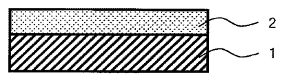
幅0.64mmのコルソン合金の角線に、厚さ0.5μmのスズ合金めっきを行った。その後、当該材料に対して、350℃で10秒間のリフロー処理を施し、図1の部分拡大概略断面図に示す角線材を得た。図1においては、角線材の1辺の中点付近の一部を拡大している(以下の各図において同様)。図1中の1は母材、2は銅スズ合金層を示す。
Example 1
A tin alloy plating with a thickness of 0.5 μm was applied to a square wire of a Corson alloy having a width of 0.64 mm. Thereafter, the material was subjected to a reflow treatment at 350 ° C. for 10 seconds to obtain a rectangular wire shown in the partially enlarged schematic sectional view of FIG. In FIG. 1, a part near the midpoint of one side of the square wire is enlarged (the same applies to the following drawings). In FIG. 1, 1 indicates a base material, and 2 indicates a copper-tin alloy layer.
比較例1
幅0.64mmのコルソン合金の角線に、厚さ0.5μmのスズ合金めっきを行った。なお、スズ合金めっき中の添加元素の量は、実施例の範囲に該当しないものとした。その後、当該材料に対して、350℃で10秒間のリフロー処理を施し、図1の部分拡大概略断面図に示す角線材を得た。
Comparative Example 1
A tin alloy plating with a thickness of 0.5 μm was applied to a square wire of a Corson alloy having a width of 0.64 mm. The amount of additive element in the tin alloy plating did not fall within the scope of the examples. Thereafter, the material was subjected to a reflow treatment at 350 ° C. for 10 seconds to obtain a rectangular wire shown in the partially enlarged schematic sectional view of FIG.
実施例2
幅0.64mmのコルソン合金の角線に、厚さ0.3μmの銅めっきを施した後、厚さ0.5μmのスズ合金めっきを行った。その後、当該材料に対して、500℃で5秒間のリフロー処理を施し、図2の部分拡大概略断面図に示す角線材を得た。図2中の1は母材、2は銅スズ合金層を示す。なお、銅めっき層は、リフロー処理によりすべて最表層のスズ合金めっきと反応し、銅スズ合金層2に転化していた。
Example 2
After applying a copper plating having a thickness of 0.3 μm to a square wire of a Corson alloy having a width of 0.64 mm, a tin alloy plating having a thickness of 0.5 μm was performed. Thereafter, the material was subjected to a reflow treatment at 500 ° C. for 5 seconds to obtain a rectangular wire shown in the partially enlarged schematic cross-sectional view of FIG. In FIG. 2, 1 indicates a base material, and 2 indicates a copper-tin alloy layer. The copper plating layer was all converted to the copper
比較例2
幅0.64mmのコルソン合金の角線に、厚さ0.3μmの銅めっきを施した後、厚さ0.5μmのスズ合金めっきを行った。なお、スズ合金めっき中の添加元素の量は、実施例の範囲に該当しないものとした。その後、当該材料に対して、350℃で10秒間のリフロー処理を施し、図2の部分拡大概略断面図に示す角線材を得た。なお、銅めっき層は、リフロー処理によりすべて最表層のスズ合金めっきと反応し、銅スズ合金層2に転化していた。
Comparative Example 2
After applying a copper plating having a thickness of 0.3 μm to a square wire of a Corson alloy having a width of 0.64 mm, a tin alloy plating having a thickness of 0.5 μm was performed. The amount of additive element in the tin alloy plating did not fall within the scope of the examples. Thereafter, the material was subjected to a reflow treatment at 350 ° C. for 10 seconds to obtain a rectangular wire shown in the partially enlarged schematic sectional view of FIG. The copper plating layer was all converted to the copper
実施例3
幅0.64mmのコルソン合金の角線に、厚さ0.4μmのニッケルめっきを施した後、厚さ0.3μmの銅めっきを施し、その後厚さ0.5μmのスズ合金めっきを行った。その後、当該材料に対して、500℃で5秒間のリフロー処理を施し、図3の部分拡大概略断面図に示す角線材を得た。図3中の1は母材、2は銅スズ合金層、3はニッケル層を示す。なお、銅めっき層は、リフロー処理によりすべて最表層のスズ合金めっきと反応し、銅スズ合金層2に転化していた。
Example 3
After applying a nickel plating with a thickness of 0.4 μm to a square wire of a Corson alloy having a width of 0.64 mm, a copper plating with a thickness of 0.3 μm was applied, and then a tin alloy plating with a thickness of 0.5 μm was performed. Thereafter, the material was subjected to a reflow treatment at 500 ° C. for 5 seconds to obtain a rectangular wire shown in the partially enlarged schematic sectional view of FIG. In FIG. 3, 1 is a base material, 2 is a copper tin alloy layer, and 3 is a nickel layer. The copper plating layer was all converted to the copper
比較例3
幅0.64mmのコルソン合金の角線に、厚さ0.4μmのニッケルめっきを施した後、厚さ0.3μmの銅めっきを施し、その後厚さ0.5μmのスズ合金めっきを行った。なお、スズ合金めっき中の添加元素の量は、実施例の範囲に該当しないものとした。その後、当該材料に対して、350℃で10秒間のリフロー処理を施し、図3の部分拡大概略断面図に示す角線材を得た。なお、銅めっき層は、リフロー処理によりすべて最表層のスズ合金めっきと反応し、銅スズ合金層2に転化していた。
Comparative Example 3
After applying a nickel plating with a thickness of 0.4 μm to a square wire of a Corson alloy having a width of 0.64 mm, a copper plating with a thickness of 0.3 μm was applied, and then a tin alloy plating with a thickness of 0.5 μm was performed. The amount of additive element in the tin alloy plating did not fall within the scope of the examples. Thereafter, the material was subjected to a reflow treatment at 350 ° C. for 10 seconds to obtain a rectangular wire shown in the partially enlarged schematic sectional view of FIG. The copper plating layer was all converted to the copper
試験例
上記実施例1〜3、比較例1〜3の角線材の接触抵抗、はんだ濡れ性、表面光沢について、評価試験を行った。これらの結果を、実施例1および比較例1については表1−1〜−2に、実施例2および比較例2については表2−1〜2−2に、実施例3および比較例3については表3−1〜3−2にそれぞれ示す。
(接触抵抗)
接触抵抗は、4端子法によって測定し、接触子にはAgプローブを用い1Nの荷重をかけて測定した。
2mΩ以内を良好であると判定して表中に「◎」で示し、5mΩ以内を合格であると判定して表中に「○」で示し、5mΩを超える場合を不合格と判定して表中に「×」で示した。
(はんだ濡れ性)
はんだ濡れ性は、メニスコグラフ法によって測定を行った。
装置はレスカ(株)製ソルダーチェッカーSAT−5100を用いた。
角線表面に、25%のロジンと残部イソプロピルアルコールから構成されるフラックスを塗布した後、260℃に保持したSn−3.0Ag−0.5Cuの鉛フリーはんだ浴に浸漬して3秒保持後、引き上げた。
判定基準は、浸漬面積の95%以上が濡れている場合に良好であると判定して表中に「◎」で示し、浸漬面積の90%以上濡れている場合に合格であると判定して表中に「○」で示し、濡れが浸漬面積の90%未満の場合を不合格と判定して表中に「×」で示した。
(表面光沢)
表面光沢を目視により検査した。むらなく均一な光沢を有するものを良好であると判定して表中に「◎」で示し、若干の鈍りはあるもののむらはなく製品として十分な光沢を有するものを合格であると判定して表中に「○」で示し、光沢不十分であるもの、またはむらが出ているものを不合格と判定して表中に「×」で示した。
Test Example An evaluation test was performed on the contact resistance, solder wettability, and surface gloss of the square wires of Examples 1 to 3 and Comparative Examples 1 to 3. These results are shown in Tables 1-1 and -2 for Example 1 and Comparative Example 1, in Tables 2-1 and 2-2 for Example 2 and Comparative Example 2, and in Example 3 and Comparative Example 3. Are shown in Tables 3-1 to 3-2, respectively.
(Contact resistance)
The contact resistance was measured by the 4-terminal method, and the contact was measured by applying a 1N load using an Ag probe.
Judged as good within 2 mΩ, indicated by “◎” in the table, judged as acceptable within 5 mΩ, indicated by “◯” in the table, and judged as unacceptable when exceeding 5 mΩ. Indicated by "x".
(Solder wettability)
Solder wettability was measured by the meniscograph method.
The apparatus used was a Solder Checker SAT-5100 manufactured by Reska Co., Ltd.
After applying a flux composed of 25% rosin and the remaining isopropyl alcohol on the surface of the square wire, it was immersed in a lead-free solder bath of Sn-3.0Ag-0.5Cu held at 260 ° C. and held for 3 seconds Raised.
Judgment criteria are determined to be good when 95% or more of the immersion area is wet and indicated as “◎” in the table, and determined to be acceptable when 90% or more of the immersion area is wet. In the table | surface, it showed with "(circle)" and the case where wetting was less than 90% of immersion area was determined to be disqualified, and it showed with "x" in the table | surface.
(Surface gloss)
The surface gloss was visually inspected. Judged that the product has a uniform and uniform glossiness is good and is indicated by “◎” in the table. The product has a slight dullness but has a sufficient glossiness as a product. In the table, it was indicated with “◯”, and those with insufficient gloss or unevenness were judged as rejected and indicated with “x” in the table.

表1−1〜1−2に示されるように、実施例1のNo.101〜107およびNo.103I〜107Iでは、いずれも接触抵抗、はんだ付け性、表面光沢の全てで基準を満たし、コネクタ等の接続部品用金属材料として好適なものであった。これに対して、比較例1のNo.111〜116およびNo.113I〜115Iでは接触抵抗、はんだ付け性、表面光沢の少なくとも1つが不合格であった。 As shown in Tables 1-1 to 1-2, No. 1 in Example 1 was obtained. 101-107 and no. In 103I to 107I, all of the contact resistance, solderability, and surface gloss met the standards, and were suitable as metal materials for connecting parts such as connectors. In contrast, No. 1 of Comparative Example 1 was used. 111-116 and no. In 113I to 115I, at least one of contact resistance, solderability, and surface gloss was unacceptable.
表2−1〜2−2に示されるように、実施例1の201〜207およびNo.203I〜207Iでは、いずれも接触抵抗、はんだ付け性、表面光沢の全てで基準を満たし、コネクタ等の接続部品用金属材料として好適なものであった。これに対して、比較例2のNo.211〜216およびNo.213I〜215Iでは接触抵抗、はんだ付け性、表面光沢の少なくとも1つが不合格であった。 As shown in Tables 2-1 to 2-2, 201-207 and No. 1 of Example 1 were used. In all of 203I to 207I, the contact resistance, solderability, and surface gloss met all the standards, and were suitable as metal materials for connecting parts such as connectors. On the other hand, the comparative example 2 No. 211-216 and no. In 213I to 215I, at least one of contact resistance, solderability, and surface gloss was unacceptable.
表3−1〜3−2に示されるように、実施例301〜307およびNo.303I〜307Iでは、いずれも接触抵抗、はんだ付け性、表面光沢の全てで基準を満たし、コネクタ等の接続部品用金属材料として好適なものであった。これに対して、比較例3のNo.311〜316およびNo.313I〜315Iでは接触抵抗、はんだ付け性、表面光沢の少なくとも1つが不合格であった。 As shown in Tables 3-1 to 3-2, Examples 301 to 307 and No. 3 were used. In 303I to 307I, all of the contact resistance, solderability, and surface glossiness were satisfied, and were suitable as metal materials for connecting parts such as connectors. On the other hand, the comparative example 3 No. 311 to 316 and No.3. In 313I to 315I, at least one of contact resistance, solderability, and surface gloss was unacceptable.
本発明をその実施態様とともに説明したが、我々は特に指定しない限り我々の発明を説明のどの細部においても限定しようとするものではなく、添付の請求の範囲に示した発明の精神と範囲に反することなく幅広く解釈されるべきであると考える。 While this invention has been described in conjunction with its embodiments, we do not intend to limit our invention in any detail of the description unless otherwise specified and are contrary to the spirit and scope of the invention as set forth in the appended claims. I think it should be interpreted widely.
1 母材
2 銅スズ合金層
3 ニッケル層
1
Claims (7)
前記最表面の銅スズ合金層は、さらに亜鉛、インジウム、アンチモン、ガリウム、鉛、ビスマス、カドミウム、マグネシウム、銀、金、アルミニウムの群から選ばれる少なくとも1種を、総量で前記スズの含有量に対する質量比で0.01%以上1%以下含有することを特徴とする接続部品用金属材料。 In a metal material for connecting parts, in which a copper or copper alloy square wire is used as a base material, and a copper tin alloy layer substantially composed of copper and tin is formed on the outermost surface thereof,
The outermost copper-tin alloy layer further includes at least one selected from the group consisting of zinc, indium, antimony, gallium, lead, bismuth, cadmium, magnesium, silver, gold, and aluminum, with respect to the content of the tin. A metal material for connecting parts, which is contained in a mass ratio of 0.01% to 1%.
Priority Applications (1)
| Application Number | Priority Date | Filing Date | Title |
|---|---|---|---|
| JP2009087559A JP5479766B2 (en) | 2008-03-31 | 2009-03-31 | Metal square wire for connecting parts and manufacturing method thereof |
Applications Claiming Priority (3)
| Application Number | Priority Date | Filing Date | Title |
|---|---|---|---|
| JP2008092053 | 2008-03-31 | ||
| JP2008092053 | 2008-03-31 | ||
| JP2009087559A JP5479766B2 (en) | 2008-03-31 | 2009-03-31 | Metal square wire for connecting parts and manufacturing method thereof |
Publications (2)
| Publication Number | Publication Date |
|---|---|
| JP2009263785A true JP2009263785A (en) | 2009-11-12 |
| JP5479766B2 JP5479766B2 (en) | 2014-04-23 |
Family
ID=41389984
Family Applications (1)
| Application Number | Title | Priority Date | Filing Date |
|---|---|---|---|
| JP2009087559A Active JP5479766B2 (en) | 2008-03-31 | 2009-03-31 | Metal square wire for connecting parts and manufacturing method thereof |
Country Status (1)
| Country | Link |
|---|---|
| JP (1) | JP5479766B2 (en) |
Cited By (4)
| Publication number | Priority date | Publication date | Assignee | Title |
|---|---|---|---|---|
| JP2009263786A (en) * | 2008-03-31 | 2009-11-12 | Furukawa Electric Co Ltd:The | Connecting component metal material and method of manufacturing the same |
| WO2014206395A1 (en) * | 2013-06-25 | 2014-12-31 | Harting Kgaa | Contact element having coating free of precious metal |
| WO2022176243A1 (en) * | 2021-02-22 | 2022-08-25 | Jx金属株式会社 | Plated material and electronic component |
| JP2022182186A (en) * | 2021-05-27 | 2022-12-08 | 石原ケミカル株式会社 | Structure including under-barrier metal and solder layer |
Citations (18)
| Publication number | Priority date | Publication date | Assignee | Title |
|---|---|---|---|---|
| JPH08176883A (en) * | 1994-12-28 | 1996-07-09 | Furukawa Electric Co Ltd:The | Production of tin alloy plated material |
| JPH11189894A (en) * | 1997-12-24 | 1999-07-13 | Murata Mfg Co Ltd | Sn alloy plated film, electronic part and chip type ceramic electronic part |
| JPH11350188A (en) * | 1998-06-03 | 1999-12-21 | Furukawa Electric Co Ltd:The | Material for electric and electronic parts, its production, and electric and electronic parts lising the same |
| JPH11350189A (en) * | 1998-06-03 | 1999-12-21 | Furukawa Electric Co Ltd:The | Material for electrical and electronic parts, its production and electrical and electronic parts using the material |
| JP2000087204A (en) * | 1998-09-17 | 2000-03-28 | Totoku Electric Co Ltd | Tin-copper alloy plated wire |
| JP2001043743A (en) * | 1999-07-29 | 2001-02-16 | Totoku Electric Co Ltd | Flat cable |
| JP2001043744A (en) * | 1999-07-29 | 2001-02-16 | Totoku Electric Co Ltd | Flat cable |
| JP2001053210A (en) * | 1999-08-11 | 2001-02-23 | Nec Corp | Lead frame, manufacture of its outer plating and manufacture of semiconductor device |
| JP2002042556A (en) * | 2000-07-28 | 2002-02-08 | Hitachi Cable Ltd | Flat cable, conductor for it, and manufacturing method thereof |
| JP2002042548A (en) * | 2000-07-19 | 2002-02-08 | Furukawa Electric Co Ltd:The | Lead wire for electronic parts and manufacturing process thereof, and electronic parts using this wire |
| WO2002103086A1 (en) * | 2001-06-18 | 2002-12-27 | Nippon Shindo Co., Ltd. | Connector wire, and manufacturing method thereof |
| JP2005105307A (en) * | 2003-09-29 | 2005-04-21 | Furukawa Electric Co Ltd:The | REFLOW-Sn-PLATED MEMBER, METHOD FOR MANUFACTURING THE MEMBER, AND COMPONENT FOR ELECTRICAL AND ELECTRONIC EQUIPMENT USING THE MEMBER |
| JP2006045665A (en) * | 2004-07-08 | 2006-02-16 | Fujikura Ltd | Flexible printed wiring board terminal and flexible flat cable terminal |
| JP2006140039A (en) * | 2004-11-12 | 2006-06-01 | Hitachi Cable Ltd | Lead wire and solar cell using the same |
| JP2007046150A (en) * | 2005-04-06 | 2007-02-22 | Misuzu:Kk | Lead wire for electronic part and flat cable comprising the same |
| JP2007299722A (en) * | 2006-04-06 | 2007-11-15 | Hitachi Cable Ltd | Wiring conductor, its manufacturing method, terminal connection part, and pb-free solder alloy |
| JP2008021501A (en) * | 2006-07-12 | 2008-01-31 | Hitachi Cable Ltd | Electrical part for wiring, manufacturing method thereof, and terminal connecting part |
| JP2009231065A (en) * | 2008-03-24 | 2009-10-08 | Fujikura Ltd | Tin-system plated rectangular conductor and flexible flat cable |
-
2009
- 2009-03-31 JP JP2009087559A patent/JP5479766B2/en active Active
Patent Citations (18)
| Publication number | Priority date | Publication date | Assignee | Title |
|---|---|---|---|---|
| JPH08176883A (en) * | 1994-12-28 | 1996-07-09 | Furukawa Electric Co Ltd:The | Production of tin alloy plated material |
| JPH11189894A (en) * | 1997-12-24 | 1999-07-13 | Murata Mfg Co Ltd | Sn alloy plated film, electronic part and chip type ceramic electronic part |
| JPH11350188A (en) * | 1998-06-03 | 1999-12-21 | Furukawa Electric Co Ltd:The | Material for electric and electronic parts, its production, and electric and electronic parts lising the same |
| JPH11350189A (en) * | 1998-06-03 | 1999-12-21 | Furukawa Electric Co Ltd:The | Material for electrical and electronic parts, its production and electrical and electronic parts using the material |
| JP2000087204A (en) * | 1998-09-17 | 2000-03-28 | Totoku Electric Co Ltd | Tin-copper alloy plated wire |
| JP2001043743A (en) * | 1999-07-29 | 2001-02-16 | Totoku Electric Co Ltd | Flat cable |
| JP2001043744A (en) * | 1999-07-29 | 2001-02-16 | Totoku Electric Co Ltd | Flat cable |
| JP2001053210A (en) * | 1999-08-11 | 2001-02-23 | Nec Corp | Lead frame, manufacture of its outer plating and manufacture of semiconductor device |
| JP2002042548A (en) * | 2000-07-19 | 2002-02-08 | Furukawa Electric Co Ltd:The | Lead wire for electronic parts and manufacturing process thereof, and electronic parts using this wire |
| JP2002042556A (en) * | 2000-07-28 | 2002-02-08 | Hitachi Cable Ltd | Flat cable, conductor for it, and manufacturing method thereof |
| WO2002103086A1 (en) * | 2001-06-18 | 2002-12-27 | Nippon Shindo Co., Ltd. | Connector wire, and manufacturing method thereof |
| JP2005105307A (en) * | 2003-09-29 | 2005-04-21 | Furukawa Electric Co Ltd:The | REFLOW-Sn-PLATED MEMBER, METHOD FOR MANUFACTURING THE MEMBER, AND COMPONENT FOR ELECTRICAL AND ELECTRONIC EQUIPMENT USING THE MEMBER |
| JP2006045665A (en) * | 2004-07-08 | 2006-02-16 | Fujikura Ltd | Flexible printed wiring board terminal and flexible flat cable terminal |
| JP2006140039A (en) * | 2004-11-12 | 2006-06-01 | Hitachi Cable Ltd | Lead wire and solar cell using the same |
| JP2007046150A (en) * | 2005-04-06 | 2007-02-22 | Misuzu:Kk | Lead wire for electronic part and flat cable comprising the same |
| JP2007299722A (en) * | 2006-04-06 | 2007-11-15 | Hitachi Cable Ltd | Wiring conductor, its manufacturing method, terminal connection part, and pb-free solder alloy |
| JP2008021501A (en) * | 2006-07-12 | 2008-01-31 | Hitachi Cable Ltd | Electrical part for wiring, manufacturing method thereof, and terminal connecting part |
| JP2009231065A (en) * | 2008-03-24 | 2009-10-08 | Fujikura Ltd | Tin-system plated rectangular conductor and flexible flat cable |
Cited By (7)
| Publication number | Priority date | Publication date | Assignee | Title |
|---|---|---|---|---|
| JP2009263786A (en) * | 2008-03-31 | 2009-11-12 | Furukawa Electric Co Ltd:The | Connecting component metal material and method of manufacturing the same |
| WO2014206395A1 (en) * | 2013-06-25 | 2014-12-31 | Harting Kgaa | Contact element having coating free of precious metal |
| WO2022176243A1 (en) * | 2021-02-22 | 2022-08-25 | Jx金属株式会社 | Plated material and electronic component |
| JP2022128101A (en) * | 2021-02-22 | 2022-09-01 | Jx金属株式会社 | Plating material for electronic component and electronic component |
| JP7155312B2 (en) | 2021-02-22 | 2022-10-18 | Jx金属株式会社 | Plating materials for electronic parts and electronic parts |
| JP2022182186A (en) * | 2021-05-27 | 2022-12-08 | 石原ケミカル株式会社 | Structure including under-barrier metal and solder layer |
| JP7197933B2 (en) | 2021-05-27 | 2022-12-28 | 石原ケミカル株式会社 | Structure including underbarrier metal and solder layer |
Also Published As
| Publication number | Publication date |
|---|---|
| JP5479766B2 (en) | 2014-04-23 |
Similar Documents
| Publication | Publication Date | Title |
|---|---|---|
| WO2009123157A1 (en) | Connecting component metal material and manufacturing method thereof | |
| JP5355935B2 (en) | Metal materials for electrical and electronic parts | |
| US8728629B2 (en) | Terminal for connector and method of producing the same | |
| EP2620275B1 (en) | Tin-plated copper-alloy material for terminal and method for producing the same | |
| CN108352639B (en) | Tin-plated copper terminal material, terminal and electric wire terminal structure | |
| EP2896724B1 (en) | Tin-plated copper-alloy terminal material | |
| EP2682263A2 (en) | Tin-plated copper-alloy material for terminal and method for producing the same | |
| JP5522300B1 (en) | Tin-plated copper alloy terminal material excellent in insertion / extraction and manufacturing method thereof | |
| JP2017203214A (en) | Copper terminal material with tin plating, terminal and wire terminal part structure | |
| JP5089451B2 (en) | Metal material for connector and manufacturing method thereof | |
| KR102352019B1 (en) | Terminal material for connector and terminal and wire terminal structure | |
| WO2009116601A1 (en) | Metallic material for connector and process for producing the metallic material for connector | |
| JP5479766B2 (en) | Metal square wire for connecting parts and manufacturing method thereof | |
| JP6620897B2 (en) | Tin-plated copper terminal material and terminal and wire terminal structure | |
| JP5479767B2 (en) | Metal square wire for connecting parts and manufacturing method thereof | |
| TWI765040B (en) | Tinned copper terminal material, terminal and wire termination structure | |
| JP5415707B2 (en) | Metal material for connector and manufacturing method thereof | |
| JP5442385B2 (en) | Conductive member and manufacturing method thereof | |
| CN113166964A (en) | Anti-corrosion terminal material, terminal and wire terminal structure | |
| JP5089452B2 (en) | Connector terminal and manufacturing method thereof | |
| JP2009230931A (en) | Connector terminal and method of manufacturing the same |
Legal Events
| Date | Code | Title | Description |
|---|---|---|---|
| A621 | Written request for application examination |
Free format text: JAPANESE INTERMEDIATE CODE: A621 Effective date: 20120201 |
|
| A977 | Report on retrieval |
Free format text: JAPANESE INTERMEDIATE CODE: A971007 Effective date: 20120501 |
|
| A131 | Notification of reasons for refusal |
Free format text: JAPANESE INTERMEDIATE CODE: A131 Effective date: 20130507 |
|
| A521 | Written amendment |
Free format text: JAPANESE INTERMEDIATE CODE: A523 Effective date: 20130704 |
|
| TRDD | Decision of grant or rejection written | ||
| A01 | Written decision to grant a patent or to grant a registration (utility model) |
Free format text: JAPANESE INTERMEDIATE CODE: A01 Effective date: 20140124 |
|
| A61 | First payment of annual fees (during grant procedure) |
Free format text: JAPANESE INTERMEDIATE CODE: A61 Effective date: 20140213 |
|
| R151 | Written notification of patent or utility model registration |
Ref document number: 5479766 Country of ref document: JP Free format text: JAPANESE INTERMEDIATE CODE: R151 |
|
| S531 | Written request for registration of change of domicile |
Free format text: JAPANESE INTERMEDIATE CODE: R313531 |
|
| R350 | Written notification of registration of transfer |
Free format text: JAPANESE INTERMEDIATE CODE: R350 |