JP2009224461A - Wiring board and method of manufacturing the same - Google Patents
Wiring board and method of manufacturing the same Download PDFInfo
- Publication number
- JP2009224461A JP2009224461A JP2008065863A JP2008065863A JP2009224461A JP 2009224461 A JP2009224461 A JP 2009224461A JP 2008065863 A JP2008065863 A JP 2008065863A JP 2008065863 A JP2008065863 A JP 2008065863A JP 2009224461 A JP2009224461 A JP 2009224461A
- Authority
- JP
- Japan
- Prior art keywords
- connection pad
- insulating layer
- pad portion
- wiring board
- wiring
- Prior art date
- Legal status (The legal status is an assumption and is not a legal conclusion. Google has not performed a legal analysis and makes no representation as to the accuracy of the status listed.)
- Pending
Links
Images


Landscapes
- Production Of Multi-Layered Print Wiring Board (AREA)
Abstract
Description
本発明は配線基板及びその製造方法に係り、さらに詳しくは、接続端子としてピンを使用するPGA(Pin Grid Array)型などの配線基板及びその製造方法に関する。 The present invention relates to a wiring board and a manufacturing method thereof, and more particularly to a wiring board of PGA (Pin Grid Array) type using pins as connection terminals and a manufacturing method thereof.
従来、接続端子としてピンを使用するPGA型の配線基板がある。図1には、従来技術のPGA型の配線基板におけるピンの周辺部が部分的に示されている。図1に示すように、従来技術のPGA型の配線基板では、層間絶縁層100の上下に形成された配線層200,220がビアホールVHを介して相互接続されている。
Conventionally, there is a PGA type wiring board that uses pins as connection terminals. FIG. 1 partially shows a peripheral portion of a pin in a conventional PGA type wiring board. As shown in FIG. 1, in the conventional PGA type wiring board,
最下の配線層220の接続パッド部Pに開口部420が設けられたソルダレジスト400が形成されている。さらに、最下の配線層220の接続パッド部Pにはんだ500によってピン600が取り付けられている。そして、配線基板のピン600がマザーボードのソケットに挿入されて電気接続される。
A solder resist 400 in which an
特許文献1には、PGA型電子部品用基板において、パッド部を形成する領域の絶縁層に凹凸を設けることでその上に形成されるパッド配線の表面を凹凸にすることにより、ピンの取り付け強度を高めることが記載されている。
また、特許文献2には、PGA型の配線基板において、ピンの径大部にSn−Agはんだより融点の高い共晶銀ロウ材からなる球面状当接部を設け、配線基板のピンパッドにピンの球面状当接部をはんだ付けすることが記載されている。
In
また、特許文献3には、配線基板の電極パッドの表面を加工して中央部に向かって窪んだ形状とすることにより、電極パッド上に形成するバンプの密着性を向上させることが記載されている。
近年では、半導体チップの高性能化に伴って配線基板の高密度化が要求されている。PGA型の配線基板では、ピンを取り付ける接続パッド部の面積が小さくなってきており、接続パッド部とピンとの接続強度が十分に得られない場合がある。 In recent years, with higher performance of semiconductor chips, higher density of wiring boards is required. In the PGA type wiring board, the area of the connection pad portion to which the pin is attached is becoming smaller, and there are cases where the connection strength between the connection pad portion and the pin cannot be sufficiently obtained.
このため、配線基板のピンをマザーボードのソケットに挿入して接続する際に、ピンが取れたりすることがあり、信頼性よくピンを挿入できないことがある。 For this reason, when inserting and connecting the pins of the wiring board to the socket of the motherboard, the pins may be removed, and the pins may not be inserted with high reliability.
さらには、配線基板の接続パッド部の面積が小さくなると、接続パッド部と層間絶縁層との密着性が十分に得られない問題がある。このため、配線基板のピンの引っ張り試験を行う際に、接続パッド部が層間絶縁層から剥がれることがあり、歩留り低下の要因になる。 Furthermore, when the area of the connection pad portion of the wiring board is reduced, there is a problem that sufficient adhesion between the connection pad portion and the interlayer insulating layer cannot be obtained. For this reason, when performing a tensile test of the pins of the wiring board, the connection pad portion may be peeled off from the interlayer insulating layer, which causes a decrease in yield.
本発明は以上の課題を鑑みて創作されたものであり、接続パッド部の面積が小さくなっても、ピンが接続パッド部に信頼性よく取り付けられる配線基板及びその製造方法を提供することを目的とする。 The present invention has been created in view of the above problems, and an object of the present invention is to provide a wiring board in which pins can be reliably attached to a connection pad portion even when the area of the connection pad portion is reduced, and a method for manufacturing the same. And
上記課題を解決するため、本発明は配線基板に係り、絶縁層の上に形成された配線層の接続パッド部にピンが立設して取り付けられた構造を有する配線基板であって、前記接続パッド部に対応する前記絶縁層の領域に一括した凹部が設けられており、前記接続パッド部の表面は前記絶縁層の凹部に対応する凹面になっていることを特徴とする。 In order to solve the above problems, the present invention relates to a wiring board, and is a wiring board having a structure in which pins are erected and attached to connection pad portions of a wiring layer formed on an insulating layer, The insulating layer corresponding to the pad portion is provided with a concave portion collectively, and the surface of the connection pad portion is a concave surface corresponding to the concave portion of the insulating layer.
本発明では、接続パッド部の下の絶縁層の領域に一括した凹部が設けられており、接続パッド部の表面が絶縁層の凹部に対応する凹面となっている。そして、接続パッド部の凹面にはんだなどによってピンが取り付けられている。 In the present invention, the concave portions collectively provided in the region of the insulating layer under the connection pad portion are provided, and the surface of the connection pad portion is a concave surface corresponding to the concave portion of the insulating layer. And the pin is attached to the concave surface of the connection pad part with solder.
接続パッド部の下の絶縁層に一括した凹部を設けることにより、接続パッド部を平坦な絶縁層の上に配置する場合よりも、接続パッド部と絶縁層との接触面積を大きく設定することができる。これにより、接続パッド部の面積が小さくなる場合であっても、接続パッド部と絶縁層との密着強度を高くすることができる。 By providing recesses collectively in the insulating layer under the connection pad portion, the contact area between the connection pad portion and the insulating layer can be set larger than when the connection pad portion is disposed on a flat insulating layer. it can. Thereby, even if it is a case where the area of a connection pad part becomes small, the adhesive strength of a connection pad part and an insulating layer can be made high.
また、本発明では、接続パッド部の表面が凹面となって窪んでいることから、ピンのヘッド部の周りにより多くのはんだを充填することができる。これにより、ピンと接続パッド部との接続強度を高めることができ、接続の信頼性を向上させることができる。 Further, in the present invention, since the surface of the connection pad portion is concave and recessed, more solder can be filled around the head portion of the pin. Thereby, the connection intensity | strength of a pin and a connection pad part can be raised, and the reliability of a connection can be improved.
本発明の一つの好適な態様では、接続パッド部の凹面は、外周側から中央部になるにつれて深さが深くなる御椀状となっている。さらに、ピンは円錐状のヘッド部を備えており、円錐状のヘッド部がはんだによって接続パッド部に固着されている。 In one preferable aspect of the present invention, the concave surface of the connection pad portion has a bowl-like shape whose depth increases from the outer peripheral side toward the central portion. Further, the pin has a conical head portion, and the conical head portion is fixed to the connection pad portion by solder.
この態様では、接続パッド部の表面を御椀状の凹面にして窪ませることにより、接続パッド部の表面がピンの円錐状のヘッド部に対応するようになるので、ピンを取り付ける際に十分な搭載安定性が得られる。これにより、ピン取り付けの信頼性を向上させることができる。 In this aspect, since the surface of the connection pad portion corresponds to the conical head portion of the pin by recessing the surface of the connection pad portion with a bowl-shaped concave surface, it is sufficient when attaching the pin. Mounting stability is obtained. Thereby, the reliability of pin attachment can be improved.
また、上記課題を解決するため、本発明は配線基板に係り、絶縁層の上に形成された配線層の接続パッド部にピンが立設して取り付けられた構造を有する配線基板であって、前記接続パッド部に対応する前記絶縁層の領域に複数の凹部が設けられており、前記接続パッド部は前記凹部を埋め込んで形成されており、かつ前記接続パッド部の表面は平坦面又は一括した凹面になっていることを特徴とする。 Further, in order to solve the above problems, the present invention relates to a wiring board, and is a wiring board having a structure in which pins are erected and attached to connection pad portions of a wiring layer formed on an insulating layer, A plurality of recesses are provided in the region of the insulating layer corresponding to the connection pad portion, the connection pad portion is formed by embedding the recess, and the surface of the connection pad portion is flat or batched. It is characterized by a concave surface.
本発明においても、接続パッド部の下の絶縁層に複数の凹部を設けることにより、接続パッド部を平坦な絶縁層の上に配置する場合よりも、接続パッド部と絶縁層との接触面積を大きく設定することができる。これにより、接続パッド部の面積が小さくなる場合であっても、接続パッド部と絶縁層との密着強度を高くすることができる。 Also in the present invention, by providing a plurality of recesses in the insulating layer under the connection pad portion, the contact area between the connection pad portion and the insulating layer can be made larger than when the connection pad portion is disposed on a flat insulating layer. Can be set large. Thereby, even if it is a case where the area of a connection pad part becomes small, the adhesive strength of a connection pad part and an insulating layer can be made high.
また、円錐状のヘッド部を備えたピンを取り付ける場合は、接続パッド部の表面を一括した凹面にすることにより、上記した発明と同様に、ピンを取り付ける際に十分な搭載安定性が得られる。 In addition, when attaching a pin having a conical head portion, sufficient mounting stability can be obtained when attaching the pin, as in the above-described invention, by making the surface of the connection pad portion into a concave surface. .
以上説明したように、本発明の配線基板では、接続パッド部の面積が小さくなっても、接続パッド部に信頼性よくピンを取り付けることができる。 As described above, in the wiring board of the present invention, even if the area of the connection pad portion is reduced, the pin can be attached to the connection pad portion with high reliability.
以下、本発明の実施の形態について、添付の図面を参照して説明する。 Hereinafter, embodiments of the present invention will be described with reference to the accompanying drawings.
(第1の実施の形態)
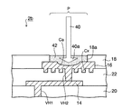
図2は本発明の第1実施形態の配線基板を示す断面図である。図2に示すように、第1実施形態の配線基板1では、コア基板10の両面側に第1配線層12がそれぞれ形成されている。コア基板10にはその厚み方向に貫通するスルーホールTHが設けられており、スルーホールTH内には貫通電極11が充填されている。そして、コア基板10の両面側の第1配線層12は貫通電極11を介して相互接続されている。
(First embodiment)
FIG. 2 is a sectional view showing the wiring board according to the first embodiment of the present invention. As shown in FIG. 2, in the
あるいは、コア基板10のスーホールTHの内面にスルーホールめっき層が設けられ、その内部の孔に樹脂が充填され、コア基板10の両面側の第1配線層12がスルーホールめっき層を介して相互接続されていてもよい。
Alternatively, a through-hole plating layer is provided on the inner surface of the so-hole TH of the
コア基板10の両面側には、第1配線層12を被覆する第1層間絶縁層20がそれぞれ形成されており、それらには第1配線層12に到達する深さの第1ビアホールVH1がそれぞれ設けられている。コア基板10の両面側の第1層間絶縁層20の上には、第1ビアホールVH1を介して第1配線層12に接続される第2配線層14がそれぞれ形成されている。
A first
さらに、コア基板10の両面側の第2配線層14の上に第2層間絶縁層22がそれぞれ形成されており、それらには第2配線層14に到達する深さの第2ビアホールVH2がそれぞれ設けられている。また、コア基板10の両面側の第2層間絶縁層22の上に第2ビアホールVH2を介して第2配線層14に接続される第3配線層16がそれぞれ形成されている。
Further, second
コア基板10の下面側の第3配線層16の接続パッド部Pの下(図2では上)に対応する第2層間絶縁層22の領域には、外周側から中央部になるにつれて深さが深くなる御椀状の凹部Cが設けられている。第3配線層16の接続パッド部Pは、第2層間絶縁層22の凹部Cの上にほぼ同一な膜厚で形成されている。これによって、第3配線層16の接続パッド部Pの表面は、第2層間絶縁層22の凹部Cに対応する凹面Caになっており、凹部Cと同様に外周側から中央部になるにつれて深さが深くなる御椀状になっている。
In the region of the second
第3配線層16の接続パッド部Pの下の第2層間絶縁層22の領域に一括した凹部Cを設けることにより、接続パッド部Pを平坦な第2層間絶縁層22の上に配置する場合よりも、接続パッド部Pと第2層間絶縁層22との接触面積を大きく設定することができる。これにより、接続パッド部Pの面積が小さくなる場合であっても、接続パッド部Pと第2層間絶縁層22との密着強度を高めることができる。
A case where the connection pad portion P is arranged on the flat second
さらに、コア基板10の両面側には、第3配線層16の接続パッド部Pの上に開口部18aが設けられたソルダレジスト18がそれぞれ形成されている。
Further, on both surface sides of the
また、コア基板10の下面側の第3配線層16の接続パッド部Pにはピン40が取り付けられている。ピン40は円錐状の径大部となるヘッド部40aを備えている。そして、ピン40のヘッド部40aがソルダレジスト18の開口部18a内の接続パッド部Pに配置されて、はんだ42によって接続パッド部Pに固着されている。ピン40は、例えば、コバールなどからなる金属ピンの表面にニッケルめっき及び金めっきが施されて構成される。ピン40は配線基板の下面側の全体又は周縁部などの部分的な領域に格子状に並んで設けられている。
A
本実施形態では、接続パッド部Pの表面が凹面Caとなって窪んでいることから、ピン40のヘッド部40aの周りにより多くのはんだ42を充填することができる。これにより、ピン40と接続パッド部Pとの接続強度を高めることができ、ピン接続の信頼性を向上させることができる。
In the present embodiment, since the surface of the connection pad portion P is recessed as a concave surface Ca,
また、接続パッド部Pの表面を御椀状の凹面Caにして窪ませることにより、接続パッド部Pの表面がピン40の円錐状のヘッド部40aに対応するようになるので、ピン40を取り付ける際に十分な搭載安定性が得られるようになり、ピン取り付けの歩留りを向上させることができる。
Moreover, since the surface of the connection pad part P corresponds to the
コア基板10の上面側の第3配線層16の接続パッド部Pには半導体チップ30のバンプ32がフリップチップ接続されている。半導体チップ30の下側の隙間にはアンダーフィル樹脂34が充填されている。そして、半導体チップ30が実装された配線基板1のピン40がマザーボードのソケットに挿入されて電気接続される。
本実施形態の配線基板1では、前述したように、接続パッド部Pの表面を凹面Caにすることでピン40のヘッド部40aを多量のはんだ42で接続パッド部Pに固着できるので、ピン40の接続強度を高めることができる。従って、マザーボードなどのソケットに配線基板1のピン40を挿入する際にピン40が取れたりする不具合が解消され、配線基板1を信頼性よくマザーボードなどに接続することができる。
In the
また、本実施形態の配線基板1では、前述したように第2層間絶縁層22の凹部Cの上に接続パッド部Pを配置してその表面を凹面Caとすることにより、平坦な第2層間絶縁層22の上に接続パッド部Pを配置する場合よりもそれらの接触面積を大きくしている。
Further, in the
これにより、接続パッド部Pと第2層間絶縁層22との密着性を向上させることできるので、設計スペックのピン引っ張り強度でピン40を引っ張っても接続パッド部Pが第2層間絶縁層22から剥がれにくくなり、引っ張りストレスに耐えることができる。
As a result, the adhesion between the connection pad portion P and the second
次に、上述した表面が凹面Caとなって窪んだ第3配線層16の接続パッド部Pを形成する方法について説明する。図3(a)に示すように、まず、前述した図2においてコア基板10の下面側の第2配線層14(下側配線層)の上に第2層間絶縁層22を形成した状態の構造体を用意する。第1、第2層間絶縁層20,22は、例えば、ポリイミド樹脂やエポキシ樹脂などの半硬化の樹脂フィルムが貼着された後に、樹脂フィルムが熱処理されて硬化することにより形成される。
Next, a method for forming the connection pad portion P of the
次いで、図3(b)に示すように、第2層間絶縁層22の接続パッド部Pが配置される領域をレーザによって加工することにより御椀状の凹部Cを形成する。凹部Cの深さdは、第2層間絶縁層22の厚みが30μmの場合、5〜10μmに設定される。なお、レーザで加工する方法以外に、接続パッド部Pが配置される領域に開口部が設けられたマスク(レジストなど)を形成し、その開口部を通して第2層間絶縁層22をエッチングして凹部Cを形成することも可能である。
Next, as shown in FIG. 3B, a region having the connection pad portion P of the second
続いて、図3(c)に示すように、第2層間絶縁層22の凹部C内のビアホールが配置される部分をレーザなどで加工することにより、第2配線層14に到達する深さの第2ビアホールVH2を形成する。なお、第2層間絶縁層22に第2ビアホールVH2を形成した後に、その周りに凹部Cを形成してもよい。
Subsequently, as shown in FIG. 3C, the portion of the second
次いで、図4(a)に示すように、第2ビアホールVH2内から第2層間絶縁層22の凹部Cの内面を含む上面に、無電解めっき又はスパッタ法により銅などからなるシード層16aを形成する。続いて、図4(b)に示すように、第3配線層が配置される部分に開口部17aが設けられためっきレジスト17を形成する。さらに、シード層16aをめっき給電経路に利用する電解めっきにより、第2ビアホールVH2内からめっきレジスト17の開口部17aに銅などからなる金属めっき層16bを形成する。
Next, as shown in FIG. 4A, a
このとき、金属めっき層16bは、第2ビアホールVH2を埋め込んで形成され、第2層間絶縁層22の凹部Cの内面上ではほぼ同一の膜厚で形成される。これにより、金属めっき層16bは、第2層間絶縁層22の凹部Cの内面上では凹部Cに対応してその表面が御椀状の凹面Caとなって窪んで形成される。
At this time, the
次いで、図4(c)に示すように、めっきレジスト17を除去した後に、金属めっき層16bをマスクにしてシード層16aをウェットエッチングすることにより、シード層16aと金属めっき層16bとにより構成される第3配線層16(上側配線層)を得る。このようにして、第2層間絶縁層22の凹部Cの上に表面が凹面Caとなった接続パッド部Pが配置される。なお、第3配線層16の形成方法として、セミアディティブ法を例示したが、サブトラクティブ法などの各種の配線形成方法を採用することができる。
Next, as shown in FIG. 4C, after the plating resist 17 is removed, the
次いで、図5(a)に示すように、第3配線層16の接続パッド部P上に開口部18aが設けられたソルダレジスト18を第2層間絶縁層22の上に形成する。
Next, as shown in FIG. 5A, a solder resist 18 having an opening 18 a provided on the connection pad portion P of the
その後に、図5(b)に示すように、円錐状のヘッド部40aを備えたピン40を用意し、はんだペーストを介してピン40のヘッド部40aを接続パッド部Pに配置し、リフロー加熱することによりピン40をはんだ42によって接続パッド部Pに固着する。このとき、前述したように、接続パッド部Pの凹面Caがピン40のヘッド部40aに対応するので、ピン40が安定して接続パッド部Pに取り付けられる。以上により、図2に示した配線基板1が得られる。
Thereafter, as shown in FIG. 5 (b), a
このような製造方法により、表面が凹面Caとなった接続パッド部Pを容易に形成できると共に、ピン40を接続パッド部Pの凹面Caに信頼性よく取り付けることができる。
With such a manufacturing method, the connection pad portion P having a concave surface Ca can be easily formed, and the
図6には、本発明の第1実施形態の第1変形例の配線基板1aが示されている。前述した配線基板1(図5(b))では、第3配線層16の接続パッド部Pの下に第2ビアホールVH2が配置されている。図6に示す第1変形例の配線基板1aのように、第3配線層16を第2ビアホールVH2から第2層間絶縁層22の上面に引き出し、第2ビアホールVH2から離れた位置に表面が御椀状の凹面Caとなった接続パッド部Pが配置されるようにしてもよい。
FIG. 6 shows a
図7には、本発明の第1実施形態の第2変形例の配線基板1bが示されている。前述した配線基板1(図5(b))では、第3配線層16の接続パッド部Pの表面を御椀状の凹面Caにしている。図7に示す第2変形例の配線基板1bのように、接続パッド部Pに対応する第2層間絶縁層22の領域に、複数の段差を有して中央部に向けて深さが深くなるような階段状の凹部Cを形成し、接続パッド部Pの表面がそれに対応する階段状の凹部になるようにしてもよい。
FIG. 7 shows a
このように、第1実施形態では、第3層間絶縁層22に形成される凹部として、一括した(内部が連通する)凹部(凹面)であれば各種の形状を採用することができ、接続パッド部Pと第3層間絶縁層22との接触面積が大きくなるようにすればよい。第1、第2変形例においても、図5(b)の配線基板1と同様な効果を奏する。
As described above, in the first embodiment, various shapes can be adopted as the recesses formed in the third
(第2の実施の形態)
図8及び図9は本発明の第2実施形態の配線基板の製造方法を示す断面図である。第2実施形態の特徴は接続パッド部の下の層間絶縁層に複数の凹部を形成することにより、接続パッド部の密着性を向上させることにある。第1実施形態と同一工程については、その詳細な説明を省略する。
(Second Embodiment)
8 and 9 are cross-sectional views showing a method of manufacturing a wiring board according to the second embodiment of the present invention. The feature of the second embodiment is that the adhesiveness of the connection pad portion is improved by forming a plurality of recesses in the interlayer insulating layer below the connection pad portion. Detailed descriptions of the same steps as those in the first embodiment are omitted.
本発明の第2実施形態の配線基板の製造方法は、図8(a)に示すように、まず、第1実施形態の図3(a)と同様に、前述した図2の配線基板においてコア基板10の下面側の第2配線層14(下側配線層)の上に第2層間絶縁層22を形成した状態の構造体を用意する。次いで、図8(b)に示すように、接続パッド部が配置される第2層間絶縁層22の領域にレーザによりホール状の複数の凹部Cxを形成する。
As shown in FIG. 8A, the method for manufacturing a wiring board according to the second embodiment of the present invention is first performed in the above-described wiring board shown in FIG. 2, as in FIG. 3A. A structure in which the second
例えば、第2層間絶縁層22の厚みが30μmの場合、各凹部Cxの深さdは5〜10μmに設定される。また、接続パッド部が配置される面積が800×800μm2の場合、その領域内に径が60μm程度の凹部Cxが複数個(例えば5〜10個)配置される。凹部Cxは、接続パッド部と第3層間絶縁層22との接触面積を大きくするために設けられるので、ホール形状の他に溝などから形成してもよいし、形状や数は任意に設定することができる。
For example, when the thickness of the second
レーザを使用する方法の他に、凹部Cxが配置される部分に開口部が設けられたマスク(レジストなど)を形成し、その開口部を通して第2層間絶縁層22をエッチングして凹部Cxを形成することも可能である。ホール形状以外の溝などの凹部Cxを形成する場合は、エッチングを採用することにより容易に形成することができる。
In addition to the method using a laser, a mask (resist or the like) having an opening is formed in a portion where the recess Cx is disposed, and the second
続いて、図8(c)に示すように、第2層間絶縁層22の凹部Cxが形成された領域の中央部をレーザなどによって加工することにより、第2配線層14に到達する深さの第2ビアホールVH2を形成する。
Subsequently, as shown in FIG. 8C, the central portion of the region where the recess Cx of the second
次いで、図8(d)に示すように、第1実施形態で説明したセミアディティブ法などにより、第2層間絶縁層22の上に第3配線層16(上側配線層)を形成する。これにより、第3配線層16の接続パッド部Pが第2層間絶縁層22の複数の凹部Cxが形成された領域の上に配置される。第3配線層16の接続パッド部Pは第2層間絶縁層22の複数の凹部Cxを埋め込んで形成され、接続パッド部Pはその下の凹部Cxに影響されることなくその表面が平坦面Sとなって形成される。
Next, as shown in FIG. 8D, the third wiring layer 16 (upper wiring layer) is formed on the second
セミアディティブ法を採用することにより、金属めっき層が第2層間絶縁層22の凹部Cxを埋め込みながら第2層間絶縁層22の上に形成されるので、凹部Cxを埋め込んで表面が平坦面Sとなる第3配線層16を容易に形成することができる。
By adopting the semi-additive method, the metal plating layer is formed on the second
さらに、図9(a)に示すように、第3配線層16の接続パッド部P上に開口部18aが設けられたソルダレジスト18を第2層間絶縁層22の上に形成する。
Further, as shown in FIG. 9A, a solder resist 18 having an opening 18 a provided on the connection pad portion P of the
その後に、図9(b)に示すように、円錐状のヘッド部40aを備えたピン40を用意し、ピン40のヘッド部40aをはんだ42によって接続パッド部Pに固着する。
Thereafter, as shown in FIG. 9B, a
以上により、第2実施形態の配線基板2が製造される。
As described above, the
第2実施形態の配線基板2では、第3配線層16の接続パッド部Pの下の第2層間絶縁層22に複数の凹部Cxを形成するので、接続パッド部Pと第2層間絶縁層22との接触面積が大きくなり、接続パッド部Pの密着性を向上させることができる。これにより、第1実施形態と同様に、設計スペックのピン引っ張り強度でピン40を引っ張っても接続パッド部Pが下の第2層間絶縁層22から剥がれにくくなり、引っ張りストレスに耐えることができる。
In the
図10には、第2実施形態の第1変形例の配線基板2aが示されている。図10に示すように、第1変形例では、第3配線層16を第2ビアホールVH2から第2層間絶縁層22の上面に引き出し、第2ビアホールVH2から離れた位置に同様な接続パッド部Pが設けられるようにしてもよい。第1変形例においても、図9(b)の配線基板2と同様な効果を奏する。
FIG. 10 shows a
また、図11には、第2実施形態の第2変形例の配線基板2bが示されている。第2実施形態の配線基板2(図9(b))では、複数の凹部Cxが接続パッド部Pによって完全に埋め込まれるため、接続パッド部Pの表面が平坦面Sとなって形成される。
In addition, FIG. 11 shows a
円錐状のヘッド部40aを備えたピン40の十分な搭載安定性を確保する必要がある場合は、図11に示す第2変形例の配線基板2bのように、接続パッド部Pの表面を加工して御椀状の凹面Caとしてもよい。第3配線層16を形成した後(ソルダレジスト18を形成する前)に、第3配線層16の表面が凹面Caに加工される。例えば、接続パッド部Pの上に開口部が設けられたマスク(レジストなど)を形成した後に、マスクの開口部を通して接続パッド部Pの表層部をウェットエッチングすることにより凹面Caを得ることができる。
When it is necessary to ensure sufficient mounting stability of the
接続パッド部Pの凹面Caは、図11のように接続パッド部Pの中央側(ピン40のヘッド部40aに対応する部分)に部分的に設けてよいし、接続パッド部Pの全体に一括して設けてもよい。
The concave surface Ca of the connection pad portion P may be provided partially on the center side of the connection pad portion P (portion corresponding to the
接続パッド部Pの全体に一括して凹面Caを設ける場合は、ソルダレジスト18の開口部18aを通して接続パッド部Pの表面をウェットエッチングすることにより凹面Caを形成してもよい。この場合は、ソルダレジスト18がそのまま残される。
When the concave surface Ca is provided all over the connection pad portion P, the concave surface Ca may be formed by wet etching the surface of the connection pad portion P through the
これにより、第1実施形態と同様に、円錐状のヘッド部40aを備えたピン40を取り付ける場合であっても、接続パッド部Pの表面形状がピン40のヘッド部40aに対応するようになるので、ピン40の十分な搭載安定性を確保することができる。
As a result, similarly to the first embodiment, even when the
1,1a,1b,2,2a,2b…配線基板、10…コア基板、11…貫通電極、12…第1配線層、14…第2配線層、16…第3配線層、16a…シード層、16b…金属めっき層、17…めっきレジスト、17a,18a…開口部、18…ソルダレジスト、20…第1層間絶縁層、22…第2層間絶縁層、30…半導体チップ、32…バンプ、34…アンダーフィル樹脂、40…ピン、40a…ヘッド部、42…はんだ、C,Cx…凹部、Ca…凹面、P…接続パッド部、S…平坦面、TH…スルーホール、VH…ビアホール。
DESCRIPTION OF
Claims (10)
前記接続パッド部に対応する前記絶縁層の領域に一括した凹部が設けられており、前記接続パッド部の表面は前記絶縁層の凹部に対応する凹面になっていることを特徴とする配線基板。 A wiring board having a structure in which pins are erected and attached to connection pad portions of a wiring layer formed on an insulating layer,
A wiring board, wherein a concave portion is provided in the insulating layer region corresponding to the connection pad portion, and a surface of the connection pad portion is a concave surface corresponding to the concave portion of the insulating layer.
前記接続パッド部に対応する前記絶縁層の領域に複数の凹部が設けられており、前記接続パッド部は前記凹部を埋め込んで形成されており、かつ前記接続パッド部の表面は平坦面又は一括した凹面になっていることを特徴とする配線基板。 A wiring board having a structure in which pins are erected and attached to connection pad portions of a wiring layer formed on an insulating layer,
A plurality of recesses are provided in the region of the insulating layer corresponding to the connection pad portion, the connection pad portion is formed by embedding the recess, and the surface of the connection pad portion is flat or batched. A wiring board having a concave surface.
下側配線層の上に前記絶縁層を形成する工程と、
前記接続パッド部に対応する前記絶縁層の領域に一括する凹部を形成すると共に、前記絶縁層に、前記下側配線層に到達するビアホールを形成する工程と、
前記ビアホール内から前記絶縁層の凹部を含む上面に繋がり、表面が前記凹部に対応する凹面となった前記接続パッド部が前記絶縁層の凹部上に配置された前記上側配線層を形成する工程と、
前記接続パッド部の凹面に前記ピンを取り付ける工程とを有することを特徴とする配線基板の製造方法。 A method for manufacturing a wiring board having a structure in which pins are erected and attached to connection pad portions of an upper wiring layer formed on an insulating layer,
Forming the insulating layer on the lower wiring layer;
Forming a recess collectively in the region of the insulating layer corresponding to the connection pad portion, and forming a via hole reaching the lower wiring layer in the insulating layer;
Forming the upper wiring layer in which the connection pad portion connected to the upper surface including the concave portion of the insulating layer from the inside of the via hole and having a concave surface corresponding to the concave portion is disposed on the concave portion of the insulating layer; ,
And a step of attaching the pin to the concave surface of the connection pad portion.
下側配線層の上に前記絶縁層を形成する工程と、
前記接続パッド部に対応する前記絶縁層の領域に複数の凹部を形成すると共に、前記絶縁層に、前記下側配線層に到達するビアホールを形成する工程と、
前記ビアホール内から前記絶縁層の複数の凹部を含む上面に繋がり、前記絶縁層の複数の凹部が形成された領域に前記凹部を埋め込んで表面が平坦面となる前記接続パッド部が配置された前記上側配線層を形成する工程と、
前記接続パッド部に前記ピンを取り付ける工程とを有することを特徴とする配線基板の製造方法。 A method for manufacturing a wiring board having a structure in which pins are erected and attached to connection pad portions of an upper wiring layer formed on an insulating layer,
Forming the insulating layer on the lower wiring layer;
Forming a plurality of recesses in the region of the insulating layer corresponding to the connection pad portion, and forming a via hole reaching the lower wiring layer in the insulating layer;
The connection pad portion that is connected to the upper surface including the plurality of recesses of the insulating layer from within the via hole, is embedded in the region where the plurality of recesses of the insulating layer are formed, and has a flat surface. Forming an upper wiring layer;
And a step of attaching the pin to the connection pad portion.
Priority Applications (1)
| Application Number | Priority Date | Filing Date | Title |
|---|---|---|---|
| JP2008065863A JP2009224461A (en) | 2008-03-14 | 2008-03-14 | Wiring board and method of manufacturing the same |
Applications Claiming Priority (1)
| Application Number | Priority Date | Filing Date | Title |
|---|---|---|---|
| JP2008065863A JP2009224461A (en) | 2008-03-14 | 2008-03-14 | Wiring board and method of manufacturing the same |
Publications (2)
| Publication Number | Publication Date |
|---|---|
| JP2009224461A true JP2009224461A (en) | 2009-10-01 |
| JP2009224461A5 JP2009224461A5 (en) | 2011-02-10 |
Family
ID=41240957
Family Applications (1)
| Application Number | Title | Priority Date | Filing Date |
|---|---|---|---|
| JP2008065863A Pending JP2009224461A (en) | 2008-03-14 | 2008-03-14 | Wiring board and method of manufacturing the same |
Country Status (1)
| Country | Link |
|---|---|
| JP (1) | JP2009224461A (en) |
Cited By (3)
| Publication number | Priority date | Publication date | Assignee | Title |
|---|---|---|---|---|
| JP2012004440A (en) * | 2010-06-18 | 2012-01-05 | Shinko Electric Ind Co Ltd | Wiring board |
| JP2012009606A (en) * | 2010-06-24 | 2012-01-12 | Shinko Electric Ind Co Ltd | Wiring board |
| JP2016096292A (en) * | 2014-11-17 | 2016-05-26 | 新光電気工業株式会社 | Wiring board, electronic component device, and method for manufacturing wiring board and electronic component device |
Citations (5)
| Publication number | Priority date | Publication date | Assignee | Title |
|---|---|---|---|---|
| JPH04322451A (en) * | 1991-04-23 | 1992-11-12 | Hitachi Ltd | Semiconductor device |
| JP2000200849A (en) * | 1999-01-06 | 2000-07-18 | Shinko Electric Ind Co Ltd | Pga-type electronic component board, manufacture thereof and semiconductor device |
| JP2001217341A (en) * | 2000-02-03 | 2001-08-10 | Ngk Spark Plug Co Ltd | Wiring board with lead pin |
| JP2003188311A (en) * | 2001-12-20 | 2003-07-04 | Kyocera Corp | Wiring board with pin and electronic device using it |
| JP2007027701A (en) * | 2005-06-13 | 2007-02-01 | Ngk Spark Plug Co Ltd | Wiring board |
-
2008
- 2008-03-14 JP JP2008065863A patent/JP2009224461A/en active Pending
Patent Citations (5)
| Publication number | Priority date | Publication date | Assignee | Title |
|---|---|---|---|---|
| JPH04322451A (en) * | 1991-04-23 | 1992-11-12 | Hitachi Ltd | Semiconductor device |
| JP2000200849A (en) * | 1999-01-06 | 2000-07-18 | Shinko Electric Ind Co Ltd | Pga-type electronic component board, manufacture thereof and semiconductor device |
| JP2001217341A (en) * | 2000-02-03 | 2001-08-10 | Ngk Spark Plug Co Ltd | Wiring board with lead pin |
| JP2003188311A (en) * | 2001-12-20 | 2003-07-04 | Kyocera Corp | Wiring board with pin and electronic device using it |
| JP2007027701A (en) * | 2005-06-13 | 2007-02-01 | Ngk Spark Plug Co Ltd | Wiring board |
Cited By (4)
| Publication number | Priority date | Publication date | Assignee | Title |
|---|---|---|---|---|
| JP2012004440A (en) * | 2010-06-18 | 2012-01-05 | Shinko Electric Ind Co Ltd | Wiring board |
| JP2012009606A (en) * | 2010-06-24 | 2012-01-12 | Shinko Electric Ind Co Ltd | Wiring board |
| JP2016096292A (en) * | 2014-11-17 | 2016-05-26 | 新光電気工業株式会社 | Wiring board, electronic component device, and method for manufacturing wiring board and electronic component device |
| US10049972B2 (en) | 2014-11-17 | 2018-08-14 | Shinko Electric Industries Co., Ltd. | Wiring board, electronic component device, method for manufacturing wiring board, and method for manufacturing electronic component device |
Similar Documents
| Publication | Publication Date | Title |
|---|---|---|
| JP5224845B2 (en) | Semiconductor device manufacturing method and semiconductor device | |
| JP4146864B2 (en) | WIRING BOARD AND MANUFACTURING METHOD THEREOF, SEMICONDUCTOR DEVICE AND SEMICONDUCTOR DEVICE MANUFACTURING METHOD | |
| JP5324051B2 (en) | Wiring substrate manufacturing method, semiconductor device manufacturing method, and wiring substrate | |
| KR101103857B1 (en) | Printed wiring board and method for manufacturing the same | |
| JP5389770B2 (en) | Printed circuit board with built-in electronic element and manufacturing method thereof | |
| JP4980295B2 (en) | Wiring substrate manufacturing method and semiconductor device manufacturing method | |
| JP6210777B2 (en) | Bump structure, wiring board, semiconductor device, and bump structure manufacturing method | |
| JP2008300507A (en) | Wiring substrate and manufacturing process of the same | |
| JP2000138313A (en) | Semiconductor device and its manufacture | |
| JP2009004772A (en) | Mounting substrate and manufacturing method thereof | |
| US9711476B2 (en) | Wiring board and electronic component device | |
| US8125064B1 (en) | Increased I/O semiconductor package and method of making same | |
| JP2000150701A (en) | Semiconductor device, connection board used therefor, and manufacture thereof | |
| TWI463931B (en) | Circuit board and method for manufacturing same | |
| JP2009194079A (en) | Wiring substrate for use in semiconductor apparatus, method for fabricating the same, and semiconductor apparatus using the same | |
| JP2006294976A (en) | Semiconductor device and its manufacturing method | |
| JP4494249B2 (en) | Semiconductor device | |
| JP2008091719A (en) | Semiconductor device | |
| KR20120019414A (en) | Wiring substrate manufacturing method | |
| JP5157455B2 (en) | Semiconductor device | |
| JP2016076534A (en) | Printed wiring board with metal post and method of manufacturing the same | |
| JP2009224461A (en) | Wiring board and method of manufacturing the same | |
| JP2010232616A (en) | Semiconductor device, and wiring board | |
| JP2007149731A (en) | Wiring board, semiconductor device, and process for producing wiring board | |
| JP4856410B2 (en) | Semiconductor device |
Legal Events
| Date | Code | Title | Description |
|---|---|---|---|
| A521 | Written amendment |
Free format text: JAPANESE INTERMEDIATE CODE: A523 Effective date: 20101216 |
|
| A621 | Written request for application examination |
Free format text: JAPANESE INTERMEDIATE CODE: A621 Effective date: 20101216 |
|
| A977 | Report on retrieval |
Free format text: JAPANESE INTERMEDIATE CODE: A971007 Effective date: 20110831 |
|
| A131 | Notification of reasons for refusal |
Effective date: 20110913 Free format text: JAPANESE INTERMEDIATE CODE: A131 |
|
| A02 | Decision of refusal |
Free format text: JAPANESE INTERMEDIATE CODE: A02 Effective date: 20120131 |