JP2007149731A - Wiring board, semiconductor device, and process for producing wiring board - Google Patents
Wiring board, semiconductor device, and process for producing wiring board Download PDFInfo
- Publication number
- JP2007149731A JP2007149731A JP2005338323A JP2005338323A JP2007149731A JP 2007149731 A JP2007149731 A JP 2007149731A JP 2005338323 A JP2005338323 A JP 2005338323A JP 2005338323 A JP2005338323 A JP 2005338323A JP 2007149731 A JP2007149731 A JP 2007149731A
- Authority
- JP
- Japan
- Prior art keywords
- metal layer
- wiring
- semiconductor device
- layer
- insulating layer
- Prior art date
- Legal status (The legal status is an assumption and is not a legal conclusion. Google has not performed a legal analysis and makes no representation as to the accuracy of the status listed.)
- Granted
Links
Images


Classifications
-
- H—ELECTRICITY
- H01—ELECTRIC ELEMENTS
- H01L—SEMICONDUCTOR DEVICES NOT COVERED BY CLASS H10
- H01L2224/00—Indexing scheme for arrangements for connecting or disconnecting semiconductor or solid-state bodies and methods related thereto as covered by H01L24/00
- H01L2224/01—Means for bonding being attached to, or being formed on, the surface to be connected, e.g. chip-to-package, die-attach, "first-level" interconnects; Manufacturing methods related thereto
- H01L2224/10—Bump connectors; Manufacturing methods related thereto
- H01L2224/15—Structure, shape, material or disposition of the bump connectors after the connecting process
- H01L2224/16—Structure, shape, material or disposition of the bump connectors after the connecting process of an individual bump connector
- H01L2224/161—Disposition
- H01L2224/16151—Disposition the bump connector connecting between a semiconductor or solid-state body and an item not being a semiconductor or solid-state body, e.g. chip-to-substrate, chip-to-passive
- H01L2224/16221—Disposition the bump connector connecting between a semiconductor or solid-state body and an item not being a semiconductor or solid-state body, e.g. chip-to-substrate, chip-to-passive the body and the item being stacked
- H01L2224/16225—Disposition the bump connector connecting between a semiconductor or solid-state body and an item not being a semiconductor or solid-state body, e.g. chip-to-substrate, chip-to-passive the body and the item being stacked the item being non-metallic, e.g. insulating substrate with or without metallisation
-
- H—ELECTRICITY
- H01—ELECTRIC ELEMENTS
- H01L—SEMICONDUCTOR DEVICES NOT COVERED BY CLASS H10
- H01L2224/00—Indexing scheme for arrangements for connecting or disconnecting semiconductor or solid-state bodies and methods related thereto as covered by H01L24/00
- H01L2224/01—Means for bonding being attached to, or being formed on, the surface to be connected, e.g. chip-to-package, die-attach, "first-level" interconnects; Manufacturing methods related thereto
- H01L2224/26—Layer connectors, e.g. plate connectors, solder or adhesive layers; Manufacturing methods related thereto
- H01L2224/31—Structure, shape, material or disposition of the layer connectors after the connecting process
- H01L2224/32—Structure, shape, material or disposition of the layer connectors after the connecting process of an individual layer connector
- H01L2224/321—Disposition
- H01L2224/32151—Disposition the layer connector connecting between a semiconductor or solid-state body and an item not being a semiconductor or solid-state body, e.g. chip-to-substrate, chip-to-passive
- H01L2224/32221—Disposition the layer connector connecting between a semiconductor or solid-state body and an item not being a semiconductor or solid-state body, e.g. chip-to-substrate, chip-to-passive the body and the item being stacked
- H01L2224/32225—Disposition the layer connector connecting between a semiconductor or solid-state body and an item not being a semiconductor or solid-state body, e.g. chip-to-substrate, chip-to-passive the body and the item being stacked the item being non-metallic, e.g. insulating substrate with or without metallisation
-
- H—ELECTRICITY
- H01—ELECTRIC ELEMENTS
- H01L—SEMICONDUCTOR DEVICES NOT COVERED BY CLASS H10
- H01L2224/00—Indexing scheme for arrangements for connecting or disconnecting semiconductor or solid-state bodies and methods related thereto as covered by H01L24/00
- H01L2224/01—Means for bonding being attached to, or being formed on, the surface to be connected, e.g. chip-to-package, die-attach, "first-level" interconnects; Manufacturing methods related thereto
- H01L2224/42—Wire connectors; Manufacturing methods related thereto
- H01L2224/47—Structure, shape, material or disposition of the wire connectors after the connecting process
- H01L2224/48—Structure, shape, material or disposition of the wire connectors after the connecting process of an individual wire connector
- H01L2224/4805—Shape
- H01L2224/4809—Loop shape
- H01L2224/48091—Arched
-
- H—ELECTRICITY
- H01—ELECTRIC ELEMENTS
- H01L—SEMICONDUCTOR DEVICES NOT COVERED BY CLASS H10
- H01L2224/00—Indexing scheme for arrangements for connecting or disconnecting semiconductor or solid-state bodies and methods related thereto as covered by H01L24/00
- H01L2224/01—Means for bonding being attached to, or being formed on, the surface to be connected, e.g. chip-to-package, die-attach, "first-level" interconnects; Manufacturing methods related thereto
- H01L2224/42—Wire connectors; Manufacturing methods related thereto
- H01L2224/47—Structure, shape, material or disposition of the wire connectors after the connecting process
- H01L2224/48—Structure, shape, material or disposition of the wire connectors after the connecting process of an individual wire connector
- H01L2224/481—Disposition
- H01L2224/48151—Connecting between a semiconductor or solid-state body and an item not being a semiconductor or solid-state body, e.g. chip-to-substrate, chip-to-passive
- H01L2224/48221—Connecting between a semiconductor or solid-state body and an item not being a semiconductor or solid-state body, e.g. chip-to-substrate, chip-to-passive the body and the item being stacked
- H01L2224/48225—Connecting between a semiconductor or solid-state body and an item not being a semiconductor or solid-state body, e.g. chip-to-substrate, chip-to-passive the body and the item being stacked the item being non-metallic, e.g. insulating substrate with or without metallisation
- H01L2224/48227—Connecting between a semiconductor or solid-state body and an item not being a semiconductor or solid-state body, e.g. chip-to-substrate, chip-to-passive the body and the item being stacked the item being non-metallic, e.g. insulating substrate with or without metallisation connecting the wire to a bond pad of the item
-
- H—ELECTRICITY
- H01—ELECTRIC ELEMENTS
- H01L—SEMICONDUCTOR DEVICES NOT COVERED BY CLASS H10
- H01L2224/00—Indexing scheme for arrangements for connecting or disconnecting semiconductor or solid-state bodies and methods related thereto as covered by H01L24/00
- H01L2224/73—Means for bonding being of different types provided for in two or more of groups H01L2224/10, H01L2224/18, H01L2224/26, H01L2224/34, H01L2224/42, H01L2224/50, H01L2224/63, H01L2224/71
- H01L2224/732—Location after the connecting process
- H01L2224/73201—Location after the connecting process on the same surface
- H01L2224/73203—Bump and layer connectors
- H01L2224/73204—Bump and layer connectors the bump connector being embedded into the layer connector
-
- H—ELECTRICITY
- H01—ELECTRIC ELEMENTS
- H01L—SEMICONDUCTOR DEVICES NOT COVERED BY CLASS H10
- H01L2224/00—Indexing scheme for arrangements for connecting or disconnecting semiconductor or solid-state bodies and methods related thereto as covered by H01L24/00
- H01L2224/73—Means for bonding being of different types provided for in two or more of groups H01L2224/10, H01L2224/18, H01L2224/26, H01L2224/34, H01L2224/42, H01L2224/50, H01L2224/63, H01L2224/71
- H01L2224/732—Location after the connecting process
- H01L2224/73251—Location after the connecting process on different surfaces
- H01L2224/73265—Layer and wire connectors
-
- H—ELECTRICITY
- H01—ELECTRIC ELEMENTS
- H01L—SEMICONDUCTOR DEVICES NOT COVERED BY CLASS H10
- H01L2924/00—Indexing scheme for arrangements or methods for connecting or disconnecting semiconductor or solid-state bodies as covered by H01L24/00
- H01L2924/15—Details of package parts other than the semiconductor or other solid state devices to be connected
- H01L2924/151—Die mounting substrate
- H01L2924/153—Connection portion
- H01L2924/1531—Connection portion the connection portion being formed only on the surface of the substrate opposite to the die mounting surface
- H01L2924/15311—Connection portion the connection portion being formed only on the surface of the substrate opposite to the die mounting surface being a ball array, e.g. BGA
Abstract
Description
本発明は、配線基板、半導体装置、及び配線基板の製造方法に係り、特に、積層された絶縁層間に配線基板の強度を補強する金属層を備えた配線基板、半導体装置、及び配線基板の製造方法に関する。 The present invention relates to a wiring board, a semiconductor device, and a manufacturing method of the wiring board, and in particular, a wiring board including a metal layer that reinforces the strength of the wiring board between laminated insulating layers, a semiconductor device, and the manufacturing of the wiring board. Regarding the method.
半導体装置は、配線基板と、配線基板と電気的に接続される半導体チップとを有した構成とされており、マザーボード等の実装基板と電気的に接続される。 The semiconductor device is configured to include a wiring board and a semiconductor chip that is electrically connected to the wiring board, and is electrically connected to a mounting board such as a mother board.
近年、電子機器の小型化に伴い、電子機器に搭載される半導体装置の小型化が望まれている。半導体装置の小型化を図ることの可能な配線基板としては、コア基材を構成から除いて薄板化したコアレス基板がある。 In recent years, with the miniaturization of electronic devices, there is a demand for miniaturization of semiconductor devices mounted on electronic devices. As a wiring board capable of reducing the size of a semiconductor device, there is a coreless board that is thinned by removing a core base material from the configuration.
しかし、コアレス基板は、コア基材を備えたコア基板と比較して強度が弱く、反りが発生しやすい。このような問題を解決するため、積層された絶縁層間に補強材としての金属層を設けたコアレス基板がある(図1参照)。 However, the coreless substrate is weaker than the core substrate provided with the core base material, and is likely to warp. In order to solve such a problem, there is a coreless substrate in which a metal layer as a reinforcing material is provided between laminated insulating layers (see FIG. 1).
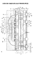
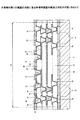
図1は、従来のコアレス基板の断面図である。図1において、W1は開口部218の上端の開口径(以下、「開口径W1」とする)、W2は開口部218の下端の開口径(以下、「開口径W2」とする)をそれぞれ示している。 FIG. 1 is a cross-sectional view of a conventional coreless substrate. In FIG. 1, W1 represents the opening diameter of the upper end of the opening 218 (hereinafter referred to as “opening diameter W1”), and W2 represents the opening diameter of the lower end of the opening 218 (hereinafter referred to as “opening diameter W2”). ing.
図1を参照するに、コアレス基板200は、絶縁層201〜204と、パッド206と、外部接続端子207と、配線208,214と、ビア209,212,215と、金属層211と、接続パッド216とを有する。
Referring to FIG. 1, the
パッド206は、絶縁層201の下面側に設けられている。外部接続端子207は、パッド206に設けられている。外部接続端子207は、コアレス基板200をマザーボード等の実装基板と電気的に接続するための端子である。配線208は、絶縁層201上に設けられており、ビア209と電気的に接続されている。ビア209は、パッド206と配線208との間に位置する絶縁層201に設けられており、パッド206と配線208とを電気的に接続している。
The pad 206 is provided on the lower surface side of the
絶縁層202は、配線208を覆うように絶縁層201上に設けられている。金属層211は、コアレス基板200の強度を補強するためのものであり、絶縁層202上に設けられている。金属層211は、板状とされており、コアレス基板200の反りを抑制する機能を奏する。金属層211は、金属箔(例えば、Cu箔)を絶縁層202上に貼り付けることで形成する。
The
絶縁層203は、金属層211を覆うように絶縁層202上に設けられている。開口部218は、配線208上に位置する絶縁層202,203を貫通するように形成されている。開口部218は、配線208上を露出している。開口部218は、ビア212を配設するためのものである。開口部218は、レーザ加工により形成される。
The
ビア212は、開口部218に設けられている。ビア212は、金属層211の下方向に配置された配線208と、金属層211の上方向に配置された配線214とを電気的に接続するためのものである。ビア212は、電解めっき法により開口部218内に導電金属を析出成長させることで形成する。
The
配線214は、絶縁層203上に設けられている。配線214は、ビア212と電気的に接続されている。絶縁層204は、配線214を覆うように絶縁層203上に設けられている。ビア215は、配線214上に位置する絶縁層204に設けられている。ビア215は、配線214と電気的に接続されている。
The
接続パッド216は、ビア215の形成位置に対応する絶縁層204上に設けられている。接続パッド216は、図示していない半導体チップを接続するためのパッドである(例えば、特許文献1参照。)。
The
このように、積層された絶縁層202,203間に金属層211を設けることで、コアレス基板200の反りを抑制することができる。
しかしながら、従来のコアレス基板200では、ビア212が配設される開口部218をレーザ加工により2層の絶縁層202,203を貫通するように形成する。このため、開口部218の深さが深くなり、開口部218の下端の開口径W2が小さくなってしまう。これにより、ビア212と配線208との間の接触面積が小さくなるため、金属層211の下方に配置された配線208と、金属層211の上方に配置された配線214との間の電気的な接続信頼性が低下してしまうという問題があった。
However, in the conventional
例えば、開口部218の下端の開口径W2を大きくするための1つの手段として、開口部218の上端の開口径W1を大きくすることが考えられるが、この場合、配線214のサイズも大きくする必要があるため、コアレス基板200が大型化して、半導体装置を小型化することができない。
For example, as one means for increasing the opening diameter W2 at the lower end of the opening 218, it is conceivable to increase the opening diameter W1 at the upper end of the opening 218. In this case, it is necessary to increase the size of the
そこで本発明は、上述した問題点に鑑みなされたものであり、本発明の目的は、配線基板の反りを抑制すると共に、電気的な接続信頼性を向上させることのできる配線基板、半導体装置、及び配線基板の製造方法を提供することである。 Therefore, the present invention has been made in view of the above-described problems, and an object of the present invention is to reduce the warpage of the wiring board and improve the electrical connection reliability, a semiconductor device, And a method of manufacturing a wiring board.
本発明の一観点によれば、積層された絶縁層と、該積層された絶縁層に設けられた配線パターンと、前記積層された絶縁層間に設けられた補強用の金属層とを備えた配線基板であって、前記金属層の直下に位置する前記絶縁層に、前記金属層と接触すると共に、前記金属層の下方に配置された前記配線パターンと電気的に接続される第1のビアを設け、前記金属層の直上に位置する前記絶縁層に、前記金属層と接触すると共に、前記金属層の上方に配置された前記配線パターンと電気的に接続される第2のビアを設けたことを特徴とする配線基板が提供される。 According to one aspect of the present invention, a wiring comprising a laminated insulating layer, a wiring pattern provided in the laminated insulating layer, and a reinforcing metal layer provided between the laminated insulating layers. A first via that is a substrate and is in contact with the metal layer and electrically connected to the wiring pattern disposed below the metal layer on the insulating layer located immediately below the metal layer. And a second via that is in contact with the metal layer and electrically connected to the wiring pattern disposed above the metal layer is provided in the insulating layer located immediately above the metal layer. Is provided.
本発明によれば、金属層の直下に位置する絶縁層に、金属層と接触すると共に、金属層の下方に配置された配線パターンと電気的に接続される第1のビアを設け、金属層の直上に位置する絶縁層に、金属層と接触すると共に、金属層の上方に配置された配線パターンと電気的に接続される第2のビアを設けたことにより、深さの浅い第1及び第2のビアを介して、金属層の上方に配置された配線パターンと、金属層の下方に配置された配線パターンとが電気的に接続される。これにより、配線パターン及び金属層と第1及び第2のビアとの間の接触面積を十分に確保することが可能となるため、金属層の上方に配置された配線パターンと、金属層の下方に配置された配線パターンとの間の電気的な接続信頼性を向上させることができる。 According to the present invention, the insulating layer located immediately below the metal layer is provided with the first via that is in contact with the metal layer and electrically connected to the wiring pattern disposed below the metal layer. By providing a second via in contact with the metal layer and electrically connected to the wiring pattern disposed above the metal layer in the insulating layer located immediately above the first and second layers having a shallow depth The wiring pattern disposed above the metal layer and the wiring pattern disposed below the metal layer are electrically connected via the second via. As a result, a sufficient contact area between the wiring pattern and the metal layer and the first and second vias can be ensured. Therefore, the wiring pattern disposed above the metal layer and the lower part of the metal layer It is possible to improve the reliability of electrical connection with the wiring pattern arranged on the board.
本発明の他の観点によれば、積層された絶縁層と、該積層された絶縁層に設けられた配線パターンと、前記積層された絶縁層間に設けられた補強用の金属層とを有する配線基板と、前記配線基板上に配設され、前記配線パターンと電気的に接続される半導体チップとを備えた半導体装置であって、前記金属層の直下に位置する前記絶縁層に、前記金属層と接触すると共に、前記金属層の下方に配置された前記配線パターンと電気的に接続される第1のビアを設け、前記金属層の直上に位置する前記絶縁層に、前記金属層と接触すると共に、前記金属層の上方に配置された前記配線パターンと電気的に接続される第2のビアを設けたことを特徴とする半導体装置が提供される。 According to another aspect of the present invention, a wiring having a laminated insulating layer, a wiring pattern provided in the laminated insulating layer, and a reinforcing metal layer provided between the laminated insulating layers. A semiconductor device comprising a substrate and a semiconductor chip disposed on the wiring substrate and electrically connected to the wiring pattern, wherein the metal layer is formed on the insulating layer located immediately below the metal layer. A first via which is electrically connected to the wiring pattern disposed below the metal layer and is in contact with the metal layer on the insulating layer located immediately above the metal layer In addition, a semiconductor device is provided in which a second via electrically connected to the wiring pattern disposed above the metal layer is provided.
本発明によれば、金属層の直下に位置する絶縁層に、金属層と接触すると共に、金属層の下方に配置された配線パターンと電気的に接続される第1のビアを設け、金属層の直上に位置する絶縁層に、金属層と接触すると共に、金属層の上方に配置された配線パターンと電気的に接続される第2のビアを設けたことにより、深さの浅い第1及び第2のビアを介して、金属層の上方に配置された配線パターンと、金属層の下方に配置された配線パターンとが電気的に接続される。これにより、配線パターン及び金属層と第1及び第2のビアとの間の接触面積を十分に確保することが可能となるため、金属層の上方に配置された配線パターンと、金属層の下方に配置された配線パターンとの間の電気的な接続信頼性を向上させることができる。 According to the present invention, the insulating layer located immediately below the metal layer is provided with the first via that is in contact with the metal layer and electrically connected to the wiring pattern disposed below the metal layer. By providing a second via in contact with the metal layer and electrically connected to the wiring pattern disposed above the metal layer in the insulating layer located immediately above the first and second layers having a shallow depth The wiring pattern disposed above the metal layer and the wiring pattern disposed below the metal layer are electrically connected via the second via. As a result, a sufficient contact area between the wiring pattern and the metal layer and the first and second vias can be ensured. Therefore, the wiring pattern disposed above the metal layer and the lower part of the metal layer It is possible to improve the reliability of electrical connection with the wiring pattern arranged on the board.
本発明のその他の観点によれば、積層された絶縁層に設けられた配線パターンと、前記積層された絶縁層間に設けられた補強用の金属層と、該金属層の直下に位置する前記絶縁層に設けられ、前記金属層及び金属層の下方に配置された前記配線パターンと電気的に接続される第1のビアと、前記金属層の直上に位置する前記絶縁層に設けられ、前記金属層及び金属層の上方に配置された前記配線パターンと電気的に接続される第2のビアとを備えた配線基板の製造方法であって、電解めっき法により前記第1のビア及び金属層を同時に形成する第1のビア及び金属層形成工程を含むことを特徴とする配線基板の製造方法が提供される。 According to another aspect of the present invention, a wiring pattern provided in a laminated insulating layer, a reinforcing metal layer provided between the laminated insulating layers, and the insulation located immediately below the metal layer A first via provided in a layer and electrically connected to the metal layer and the wiring pattern disposed below the metal layer; and provided in the insulating layer located immediately above the metal layer; A method of manufacturing a wiring board comprising a second via electrically connected to the wiring pattern disposed above the metal layer and the metal layer, wherein the first via and the metal layer are formed by electrolytic plating. There is provided a method for manufacturing a wiring board including a first via and metal layer forming step formed simultaneously.
本発明によれば、電解めっき法を用いて、第1のビア及び金属層を同時に形成することにより、製造工程を簡略化して、配線基板の製造コストを低減することができる。 According to the present invention, the first via and the metal layer are simultaneously formed using the electrolytic plating method, whereby the manufacturing process can be simplified and the manufacturing cost of the wiring board can be reduced.
本発明によれば、配線基板の反りを抑制すると共に、電気的な接続信頼性を向上させることができる。 ADVANTAGE OF THE INVENTION According to this invention, while suppressing the curvature of a wiring board, electrical connection reliability can be improved.
次に、図面に基づいて本発明の実施の形態について説明する。 Next, embodiments of the present invention will be described with reference to the drawings.
(第1の実施の形態)
図2は、本発明の第1の実施の形態に係る半導体装置の断面図である。
(First embodiment)
FIG. 2 is a cross-sectional view of the semiconductor device according to the first embodiment of the present invention.
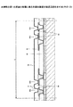
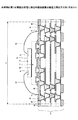
図2を参照して、本発明の第1の実施の形態に係る半導体装置10について説明する。半導体装置10は、配線基板11と、外部接続端子12と、第1の半導体チップ14と、第2の半導体チップ15と、封止樹脂16とを有する。
A
配線基板11は、絶縁層18,26,32,38と、パッド19と、保護膜20,49と、配線パターン21と、補強用の金属層27と、第1のビア28と、第2のビア33と、拡散防止膜51とを有する。
The
絶縁層18,26,32,38は、絶縁層18、絶縁層26、絶縁層32、絶縁層38の順に積層されている。絶縁層18,26,32,38としては、例えば、エポキシ系樹脂やポリイミド系樹脂等を用いることができる。また、絶縁層18,26,32,38の厚さは、例えば、それぞれ30μm〜50μmとすることができる。
The insulating layers 18, 26, 32 and 38 are laminated in the order of the insulating
パッド19は、絶縁層18から露出された状態で、絶縁層18の下面18B側に設けられている。絶縁層18から露出されたパッド19の面19Aは、絶縁層18の下面18Bと略面一とされている。パッド19は、外部接続端子12及びビア22と電気的に接続されている。パッド19としては、絶縁層18からNi層、Pd層、Au層を順次積層したNi/Pd/Au積層膜を用いることができる。
The
保護膜20は、パッド19を露出した状態で、絶縁層18の下面18Bを覆うように設けられている。保護膜20としては、例えば、ソルダーレジストを用いることができる。保護膜20の厚さは、例えば、20μmとすることができる。
The
配線パターン21は、金属層27の上方及び下方に配置されている。配線パターン21は、ビア22,39,41と、配線24,35,36,43,46とを有する。
The
ビア22は、パッド19上に位置する絶縁層18を貫通するように設けられている。ビア22は、パッド19及び配線24と電気的に接続されている。配線24は、絶縁層18の上面18Aに設けられている。配線24は、ビア22及び第1のビア28と電気的に接続されている。ビア22及び配線24は、金属層27の下方に配置された配線パターン21である。
The via 22 is provided so as to penetrate the insulating
配線35は、絶縁層32上に設けられている。配線35は、第2のビア33及びビア39と電気的に接続されている。配線36は、配線35の形成位置よりも内側に位置する絶縁層32上に設けられている。配線36は、第2のビア33及びビア41と電気的に接続されている。ビア39は、配線35上に位置する絶縁層38を貫通するように設けられている。ビア39は配線35,43と電気的に接続されている。
The
ビア41は、配線36上に位置する絶縁層38を貫通するように設けられている。ビア41は、配線36,46と電気的に接続されている。配線43は、接続部44を有しており、絶縁層38上に設けられている。接続部44は、ワイヤ63を電気的に接続するためのものである。配線43は、ビア39及びワイヤ63と電気的に接続されている。
The via 41 is provided so as to penetrate the insulating
配線46は、接続部47を有しており、絶縁層38上に設けられている。接続部47は、第1の半導体チップ14をフリップチップ接続するためのものである。配線46は、第1の半導体チップ14及びビア41と電気的に接続されている。配線35,36,43,46及びビア39,41は、金属層27の上方に配置された配線パターン21である。
The
上記構成とされた配線パターン21の材料としては、導電金属を用いることができ、導電金属としては、例えば、Cuを用いることができる。配線24,35,36,43,46の厚さは、例えば、20μmとすることができる。
As the material of the
補強用の金属層27は、薄板状とされており、積層された絶縁層18,26,32,38の略中間に位置する絶縁層26上に設けられている。金属層27は、配線基板11の反りを抑制するための層である。金属層27は、例えば、電解めっき法により形成することができる。金属層27の材料としては、例えば、Cu、Ni、Co、Fe、Ni−Co合金、Ni−Fe合金等を用いることができる。金属層27の厚さは、例えば、10μm〜30μmとすることができる。
The reinforcing
第1のビア28は、配線24と金属層27との間に位置する絶縁層26(金属層27の直下に位置する絶縁層)を貫通するように設けられている。第1のビア28は、金属層27と接触しており、配線24及び金属層27と電気的に接続されている。第1のビア28は、金属層27の下方に配置された配線パターン21(具体的には、ビア22及び配線24)と金属層27との間を電気的に接続している。第1のビア28は、図1(従来例)に示した金属層211の下方に配置された配線208と、金属層211の上方に配置された配線214との間を電気的に接続する従来のビア212よりも深さの浅いビアである。第1のビア28の深さは、従来のビア212の略半分とされている。第1のビア28の材料としては、例えば、Cu、Ni、Co、Fe、Ni−Co合金、Ni−Fe合金等を用いることができる。第1のビア28は、レーザ加工により絶縁層26に開口部(図13に示す開口部26A)を形成し、この開口部に導電金属を充填することで形成する。第1のビア28を構成する導電金属は、例えば、電解めっき法により形成することができる。
The first via 28 is provided so as to penetrate the insulating layer 26 (insulating layer located immediately below the metal layer 27) located between the
第2のビア33は、金属層27と配線35,36との間に位置する絶縁層32(金属層27の直上に位置する絶縁層)を貫通するように設けられている。第2のビア33は、金属層27と接触しており、配線35,36及び金属層27と電気的に接続されている。第2のビア33は、金属層27の上方に配置された配線パターン21(具体的には、配線35,36,43,46及びビア39,41)と金属層27との間を電気的に接続している。また、第2のビア33は、金属層27を挟んで、第1のビア28と対向するように配置されている。
The second via 33 is provided so as to penetrate the insulating layer 32 (insulating layer positioned immediately above the metal layer 27) located between the
このように、第2のビア33を第1のビア28と対向するように配置することにより、金属層27の下方に配置された配線パターン21(具体的には、ビア22及び配線24)と、金属層27の上方に配置された配線パターン21(具体的には、配線35,36,43,46及びビア39,41)との間の接続距離を短くすることができる。
Thus, by arranging the second via 33 so as to oppose the first via 28, the wiring pattern 21 (specifically, the via 22 and the wiring 24) arranged below the
第2のビア33は、図1(従来例)に示した金属層211の下方に配置された配線208と、金属層211の上方に配置された配線214との間を電気的に接続する従来のビア212よりも深さの浅いビアである。第2のビア33の深さは、従来のビア212の略半分とされている。第2のビア33の材料としては、例えば、導電金属を用いることができ、導電金属としては、例えば、Cuを用いることができる。第2のビア33は、レーザ加工により絶縁層32に開口部(図18に示す開口部32A)を形成し、この開口部に導電金属を充填することで形成する。第2のビア33を構成する導電金属は、例えば、電解めっき法により形成することができる。
The second via 33 electrically connects the
このように、金属層27の直下に位置する絶縁層26に、金属層27と接触すると共に、金属層27の下方に配置された配線パターン21(具体的には、ビア22及び配線24)と電気的に接続される第1のビア28を設け、金属層27の直上に位置する絶縁層32に、金属層27と接触すると共に、金属層27の上方に配置された配線パターン21(具体的には、配線35,36,43,46及びビア39,41)と電気的に接続される第2のビア33を設けたことにより、深さの浅い第1及び第2のビア28,33を介して、金属層27の上方に配置された配線パターン21と、金属層27の下方に配置された配線パターン21との間が電気的に接続される。これにより、配線パターン21及び金属層27と第1及び第2のビア28,33との間の接触面積を十分に確保することが可能となるため、金属層27の上方に配置された配線パターン21と、金属層27の下方に配置された配線パターン21との間の電気的な接続信頼性を向上させることができる。
As described above, the insulating
また、第2のビア33を第1のビア28と対向するように配置することにより、金属層27の下方に配置された配線パターン21と、金属層27の上方に配置された配線パターン21との間の接続距離を短くすることができる。
In addition, by arranging the second via 33 so as to face the first via 28, the
保護膜49は、接続部44,47以外の配線43,46を覆うように絶縁層38上に設けられている。保護膜49としては、例えば、ソルダーレジストを用いることができる。保護膜49の厚さは、例えば、20μmとすることができる。
The
拡散防止膜51は、配線43に含まれるCuの拡散を防止すると共に、ワイヤ63と配線43との間の接続信頼性を向上させるための膜である。拡散防止膜51としては、例えば、配線43上に、Ni層、Au層の順に積層したNi/Au積層層を用いることができる。
The
外部接続端子12は、パッド19の面19Aに設けられている。外部接続端子12は、半導体装置10をマザーボード等の実装基板に接続するための端子である。外部接続端子12としては、例えば、はんだボールを用いることができる。
The
第1の半導体チップ14は、配線基板11上に配設されている。第1の半導体チップ14は、チップ本体53と、電極パッド54と、スタッドバンプ56とを有する。チップ本体53は、半導体基板(図示せず)と、半導体素子(図示せず)と、多層配線構造体(図示せず)とを有する。半導体基板(図示せず)は、チップ本体の上面53A側に設けられている。半導体基板(図示せず)としては、例えば、Si基板やGa−As基板等を用いることができる。半導体素子(図示せず)は、トランジスタ等の素子であり、半導体基板(図示せず)に設けられている。
The
電極パッド54は、チップ本体53の下面53B側に設けられている。電極パッド54は、多層配線構造体(図示せず)を介して、半導体素子(図示せず)と電気的に接続されている。
The
スタッドバンプ56は、電極パッド54に設けられている。スタッドバンプ56は、はんだ57を介して、配線46の接続部47と電気的に接続されている。これにより、第1の半導体チップ14は、配線パターン21と電気的に接続される。スタッドバンプ56は、第1の半導体チップ14を接続部47にフリップチップ接続するためのものである。スタッドバンプ56としては、例えば、Auスタッドバンプを用いることができる。
The
第1の半導体チップ14と配線基板11との間には、アンダーフィル樹脂58が充填されている。アンダーフィル樹脂58は、第1の半導体チップ14と配線基板11との間の接合強度を向上させるための樹脂である。
An
第2の半導体チップ15は、接着材62により第1の半導体チップ14上に接着されている。第2の半導体チップ15は、第1の半導体チップ14よりも外形の小さい半導体チップであり、チップ本体59と、電極パッド61とを有する。チップ本体59は、半導体基板(図示せず)と、半導体素子(図示せず)と、多層配線構造体(図示せず)とを有する。半導体基板(図示せず)は、チップ本体59の下面59B側に設けられている。半導体基板(図示せず)としては、例えば、Si基板やGa−As基板等を用いることができる。半導体素子(図示せず)は、トランジスタ等の素子であり、半導体基板(図示せず)に設けられている。
The
電極パッド61は、チップ本体59の上面59A側に設けられている。電極パッド61は、多層配線構造体(図示せず)を介して、半導体素子(図示せず)と電気的に接続されている。また、電極パッド61は、ワイヤ63を介して、配線パターン21と電気的に接続(ワイヤボンディング接続)されている。
The
ワイヤ63は、一方の端部が電極パッド61と接続されており、他方の端部が拡散防止膜51と電気的に接続されている。封止樹脂16は、配線基板11上に設けられており、第1及び第2の半導体チップ14,15とワイヤ63とを封止している。封止樹脂16としては、例えば、エポキシ系樹脂を用いることができる。
One end of the
本実施の形態の半導体装置によれば、金属層27の直下に位置する絶縁層26に、金属層27と接触すると共に、金属層27の下方に配置された配線パターン21(具体的には、ビア22及び配線24)と電気的に接続される第1のビア28を設け、金属層27の直上に位置する絶縁層32に、金属層27と接触すると共に、金属層27の上方に配置された配線パターン21(具体的には、配線35,36,43,46及びビア39,41)と電気的に接続される第2のビア33を設けたことにより、深さの浅い第1及び第2のビア28,33を介して、金属層27の上方に配置された配線パターン21と、金属層27の下方に配置された配線パターン21との間が電気的に接続される。これにより、配線パターン21及び金属層27と第1及び第2のビア28,33との間の接触面積を十分に確保することが可能となるため、金属層27の上方に配置された配線パターン21と、金属層27の下方に配置された配線パターン21との間の電気的な接続信頼性を向上させることができる。
According to the semiconductor device of the present embodiment, the wiring pattern 21 (specifically, the insulating
また、第2のビア33を第1のビア28と対向するように配置することにより、金属層27の下方に配置された配線パターン21と、金属層27の上方に配置された配線パターン21との間の接続距離を短くすることができる。
In addition, by arranging the second via 33 so as to face the first via 28, the
図3〜図28は、本発明の第1の実施の形態に係る半導体装置の製造工程を示す図である。図3〜図28において、第1の実施の形態の半導体装置10と同一構成部分には同一符号を付す。また、図3〜図27において、Eは半導体装置10が形成される領域(以下、「半導体装置形成領域E」とする)を示している。
3 to 28 are views showing a manufacturing process of the semiconductor device according to the first embodiment of the present invention. 3 to 28, the same components as those of the
図3〜図28を参照して、第1の実施の形態の半導体装置10の製造方法について説明する。なお、図3〜図28では、支持板71上に複数の半導体装置10を製造する場合を例に挙げて説明する。
A method for manufacturing the
始めに、図3に示す工程では、導電金属からなる支持板71上に開口部20Aを有した保護膜20を形成する。支持板71は、複数の半導体装置10を製造可能な支持板である。支持板71としては、例えば、Cu等の金属板または金属箔を用いることができる。開口部20Aは、パッド19の形成位置に対応している。保護膜20は、例えば、印刷法により形成することができる。保護膜20としては、例えば、ソルダーレジストを用いることができる。また、保護膜20の厚さは、例えば、20μmとすることができる。
First, in the step shown in FIG. 3, the
具体的には、例えば、印刷法により、Cu板上にソルダーレジストを塗布し、その後、開口部20Aの形成位置に対応するソルダーレジストを露光、現像することで、保護膜20を形成する。
Specifically, for example, the
次いで、図4に示す工程では、開口部20Aにパッド19の高さ方向の位置を調整するための導電金属72を形成する。導電金属72としては、例えば、Cuを用いることができる。具体的には、支持板71を給電層とする電解めっき法により、開口部20Aに導電金属72を析出成長させる。
Next, in the step shown in FIG. 4, a
次いで、図5に示すように、導電金属72上にパッド19を形成する。パッド19としては、例えば、導電金属72上にAu層、Pd層、Ni層を順次積層したNi/Pd/Au積層膜を用いることができる。具体的には、電解めっき法により、導電金属72上にAu層、Pd層、Ni層を順次積層して、パッド19を形成する。
Next, as shown in FIG. 5, the
次いで、図6に示す工程では、パッド19及び保護膜20を覆うように絶縁層18を形成する。絶縁層18は、例えば、印刷法や樹脂フィルムの積層により形成することができる。
絶縁層18としては、例えば、エポキシ系樹脂やポリイミド系樹脂等を用いることができる。保護膜20上における絶縁層18の厚さは、例えば、30μm〜50μmとすることができる。
Next, in the step shown in FIG. 6, the insulating
As the insulating
次いで、図7に示す工程では、レーザ加工により、絶縁層18にパッド19上を露出する開口部18Cを形成する。次いで、図8に示す工程では、開口部18Cと絶縁層18の上面18Aとを覆うようにシード層74を形成する。シード層74は、無電解めっき法、スパッタ法、真空蒸着法等により形成できる。シード層74の材料としては、例えば、CuやNi等を用いることができる。
Next, in a step shown in FIG. 7, an
次いで、図9に示す工程では、図8に示した構造体上に、シード層74を露出する開口部75Aを有したレジスト膜75を形成する。開口部75Aは、配線24の形状及び形成位置に対応している。
Next, in a process shown in FIG. 9, a resist
次いで、図10に示す工程では、シード層74を給電層とする電解めっき法により、レジスト膜75の開口部75Aに露出されたシード層74上に導電金属77を形成する。これにより、開口部18Cにはシード層74及び導電金属77からなるビア22が形成され、絶縁層18上にはシード層74及び導電金属77からなる配線24が形成される。
Next, in a step shown in FIG. 10, a
なお、この段階において、複数の配線24は、絶縁層18上に形成されたシード層74により隣り合う配線24と電気的に接続されている。導電金属77としては、例えば、Cuを用いることができる。また、配線24の厚さは、例えば、20μmとすることができる。
At this stage, the plurality of
次いで、図11に示す工程では、レジスト膜75を除去する。次いで、図12に示す工程では、導電金属77に覆われていない不要なシード層74をエッチングにより除去する。これにより、複数の配線24は、隣り合う他の配線24と電気的に分離される。
Next, in the step shown in FIG. 11, the resist
次いで、図13に示す工程では、図12に示した構造体上に、配線24の上面を露出する開口部26Aを有した絶縁層26を形成する。開口部26Aは、第1のビア28の形状及び形成位置に対応している。絶縁層26は、例えば、印刷法や樹脂フィルムの積層により形成することができる。絶縁層26としては、例えば、エポキシ系樹脂やポリイミド系樹脂等を用いることができる。絶縁層18上における絶縁層26の厚さは、例えば、30μm〜50μmとすることができる。
Next, in a process shown in FIG. 13, an insulating
次いで、図14に示す工程では、開口部26Aと絶縁層26の上面とを覆うようにシード層79を形成する。シード層79は、無電解めっき法、スパッタ法、真空蒸着法等により形成できる。シード層79の材料としては、例えば、Cu、Ni等を用いることができる。
Next, in the step shown in FIG. 14, a
次いで、図15に示す工程では、図14に示した構造体上に、シード層79を露出する開口部80Aを有したレジスト膜80を形成する。開口部80Aは、金属層27の形状及び形成位置に対応している。
Next, in a step shown in FIG. 15, a resist
次いで、図16に示す工程では、シード層79を給電層とする電解めっき法により、レジスト膜80の開口部80Aに露出されたシード層79上に導電金属82を形成する(第1のビア及び金属層形成工程)。これにより、シード層79及び導電金属82からなる第1のビア28と、シード層79及び導電金属82からなる金属層27とが同時に形成される。導電金属82としては、例えば、Cu、Ni、Co、Fe、Ni−Co合金、Ni−Fe合金等を用いることができる。また、金属層27の厚さは、例えば、10μm〜30μmとすることができる。
Next, in the step shown in FIG. 16, a
このように、電解めっき法により、第1のビア28と金属層27とを同時に形成することで、製造工程が簡略化されるので、半導体装置10及び配線基板11の製造コストを低減することができる。
Thus, since the manufacturing process is simplified by simultaneously forming the first via 28 and the
また、電解めっき法により金属層27を形成することで、金属層27の厚さが所望の厚さとなるように容易に調整することができる。
Further, by forming the
次いで、図17に示す工程では、レジスト膜80を除去し、その後、導電金属82に覆われていない不要なシード層79を除去する。これにより、第1及び第2のビア28,33と接触する金属層27部分は、他の金属層27部分と電気的に分離される。
Next, in the step shown in FIG. 17, the resist
次いで、図18に示す工程では、先に説明した図6及び図7の工程と同様な手法により、図17に示した構造体上に、金属層27を露出する開口部32Aを有した絶縁層32を形成する。開口部32Aは、第2のビア33を配設するためのものであり、第2のビア33の形状及び形成位置に対応している。開口部32Aは、例えば、レーザ加工を用いて、第1のビア28と対向するように形成する。
Next, in the step shown in FIG. 18, an insulating layer having an
このように、第2のビア33が配設される開口部32Aを第1のビア28と対向するように形成することにより、開口部32Aを形成する際、レーザが金属層27を貫通した場合でも、第1のビア28内で開口部32Aの底面及び側壁をストップさせることが可能となる。これにより、第1のビア28と第2のビア33との間の電気的な接続が確保され、配線基板11の歩留まりを向上させることができる。
In this way, when the
絶縁層32は、例えば、印刷法や樹脂フィルムの積層により形成することができる。絶縁層32としては、例えば、エポキシ系樹脂やポリイミド系樹脂等を用いることができる。絶縁層26上における絶縁層32の厚さは、例えば、30μm〜50μmとすることができる。
The insulating
続いて、先に説明した図8〜図12の工程と同様な手法により、シード層83及び導電金属84からなる第2のビア33と、シード層83及び導電金属84からなる配線35,36とを同時に形成する(第2のビア形成工程)。シード層83の材料としては、例えば、Cu、Ni等を用いることができる。導電金属84としては、例えば、Cuを用いることができる。また、配線35,36の厚さは、例えば、20μmとすることができる。
Subsequently, the second via 33 made of the
次いで、図19に示す工程では、先に説明した図6及び図7の工程と同様な手法により、図18に示した構造体上に開口部38A,38Bを有した絶縁層38を形成する。開口部38Aは、ビア39の形状及び形成位置に対応しており、ビア39を配設するためのものである。開口部38Aは、配線35の上面を露出するように形成する。開口部38Bは、ビア41の形状及び形成位置に対応しており、ビア41を配設するためのものである。開口部38Bは、配線36の上面を露出するように形成する。絶縁層38は、例えば、印刷法や樹脂フィルムの積層によりにより形成することができる。絶縁層38としては、例えば、エポキシ系樹脂やポリイミド系樹脂等を用いることができる。絶縁層32上の絶縁層38の厚さは、例えば、30μm〜50μmとすることができる。
Next, in the step shown in FIG. 19, the insulating
続いて、先に説明した図8〜図12の工程と同様な手法により、シード層86及び導電金属87からなるビア39,41と、シード層86及び導電金属87からなる配線43,46とを同時に形成する。シード層86の材料としては、例えば、Cu、Ni等を用いることができる。また、導電金属87としては、例えば、Cuを用いることができる。配線43,46の厚さは、例えば、20μmとすることができる。
Subsequently, the
次いで、図20に示す工程では、絶縁層38上に、接続部44,47以外の配線43,46部分を覆うように保護膜49を形成する。保護膜49は、例えば、印刷法により形成することができる。保護膜49としては、例えば、ソルダーレジストを用いることができる。保護膜49の厚さは、例えば、20μmとすることができる。次いで、図21に示す工程では、図20に示した構造体上に接続部44のみを露出する開口部89Aを有したレジスト膜89を形成する。
Next, in the step shown in FIG. 20, a
次いで、図22に示す工程では、配線43を給電層とする電解めっき法により、接続部44上に拡散防止膜51を形成する。拡散防止膜51としては、例えば、接続部44上に、Ni層、Au層の順に積層したNi/Au積層膜を用いることができる。
Next, in the step shown in FIG. 22, the
次いで、図23に示す工程では、レジスト膜89を除去する。次いで、図24に示す工程では、エッチングにより、支持板71及び導電金属72を除去する。これにより、配線基板11が製造される。
Next, in the step shown in FIG. 23, the resist film 89 is removed. Next, in the step shown in FIG. 24, the
次いで、図25に示す工程では、接続部47上にはんだ57を塗布し、はんだ57を溶融させた後、スタッドバンプ56を接続部47に接触させてスタッドバンプ56と接続部47とを接続する。これにより、第1の半導体チップ14は、配線基板11とフリップチップ接続される。続いて、第1の半導体チップ14と配線基板11との間にアンダーフィル樹脂58を充填する。
Next, in the process shown in FIG. 25,
次いで、図26に示す工程では、接着材62により、第1の半導体チップ14上に第2の半導体チップ15を接着する。続いて、電極パッド61と拡散防止膜51との間を電気的に接続するワイヤ63を形成する。これにより、第2の半導体チップ15は、配線基板11に対してワイヤボンディング接続される。
Next, in the process shown in FIG. 26, the
次いで、図27に示す工程では、図26に示した構造体上に、第1及び第2の半導体チップ14,15とワイヤ63とを封止するように封止樹脂16を形成する。封止樹脂16は、例えば、トランスファーモールド法により形成することができる。封止樹脂16としては、例えば、エポキシ系樹脂を用いることができる。
Next, in a step shown in FIG. 27, a sealing
次いで、図28に示す工程では、パッド19に外部接続端子12を形成し、その後、ダイシングにより、半導体装置形成領域Eの外形位置(図27参照)に対応する封止樹脂16及び絶縁層18,26,32,38を切断して、複数の半導体装置10を製造する。
Next, in the process shown in FIG. 28, the
本実施の形態の製造方法によれば、電解めっき法を用いて、第1のビア28と金属層27とを同時に形成することにより、製造工程を簡略化して、半導体装置10及び配線基板11の製造コストを低減することができる。
According to the manufacturing method of the present embodiment, the first via 28 and the
また、第2のビア33が配設される開口部32Aを第1のビア28と対向するように形成することにより、レーザが金属層27を貫通した場合でも、第1のビア28内で開口部32Aの底面及び側壁をストップさせることが可能となるため、第1のビア28と第2のビア33との間の電気的な接続が確保され、配線基板11の歩留まりを向上させることができる。
Further, by forming the
なお、支持板71及び導電金属72の除去は、配線基板11上に第1及び第2の半導体チップ14,15を実装して封止樹脂16を形成した後に行なってもよい。
The
(第2の実施の形態)
図29は、本発明の第2の実施の形態に係る半導体装置の断面図である。図29において、第1の実施の形態の半導体装置10と同一構成部分には同一符号を付す。
(Second Embodiment)
FIG. 29 is a sectional view of a semiconductor device according to the second embodiment of the present invention. In FIG. 29, the same components as those of the
図29を参照して、本発明の第2の実施の形態に係る半導体装置95について説明する。半導体装置95は、外部接続端子12と、第1の半導体チップ14と、第2の半導体チップ15と、封止樹脂16と、金属層97を備えた配線基板96とを有する。半導体装置95は、第1の実施の形態の半導体装置10に設けられた金属層27の代わりに金属層97を設けた以外は半導体装置10と同様に構成される。
A semiconductor device 95 according to the second embodiment of the present invention will be described with reference to FIG. The semiconductor device 95 includes an
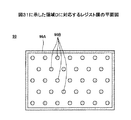
図30は、図29に示した領域Aに対応する金属層の平面図である。 FIG. 30 is a plan view of the metal layer corresponding to region A shown in FIG.
図29及び図30を参照するに、金属層97は、絶縁層26上に設けられている。金属層97は、複数の貫通孔97A(第1の貫通孔)を有した以外は、第1の実施の形態で説明した金属層27と同様に構成される。複数の貫通孔97Aは、金属層97の全面に亘って形成されている。複数の貫通孔97Aは、例えば、千鳥状、或いは、格子状に配置することができる。図30では、複数の貫通孔97Aを千鳥状に配置した場合を図示している。貫通孔97Aは、例えば、円柱、四角柱等の形状とすることができる。貫通孔97Aの形状が円柱の場合、貫通孔97Aの直径は、例えば、30μm〜300μmとすることができる。
Referring to FIGS. 29 and 30, the
本実施の形態の半導体装置によれば、金属層27の代わりに複数の貫通孔97Aを有した金属層97を絶縁層26上に設けることにより、複数の貫通孔97A内を絶縁層32で充填して、絶縁層26と絶縁層32との接触面積を増加させて、絶縁層26,32間の密着性を向上させることができる。
According to the semiconductor device of the present embodiment, the
また、複数の貫通孔97Aは、製造時に絶縁層18,26,32,38から発生するガスを放出するためのガス抜き孔として利用することができる。
Further, the plurality of through
図31及び図32は、本発明の第2の実施の形態に係る半導体装置の製造工程を示す図である。図33は、図31に示した領域Dに対応するレジスト膜の平面図である。図31〜図33において、第2の実施の形態の半導体装置95と同一構成部分には同一符号を付す。 31 and 32 are views showing a manufacturing process of the semiconductor device according to the second embodiment of the present invention. FIG. 33 is a plan view of a resist film corresponding to the region D shown in FIG. 31 to 33, the same components as those of the semiconductor device 95 of the second embodiment are denoted by the same reference numerals.
図31〜図33を参照して、本発明の第2の実施の形態に係る半導体装置95の製造方法について説明する。 With reference to FIGS. 31 to 33, a method of manufacturing the semiconductor device 95 according to the second embodiment of the present invention will be described.
始めに、先に説明した図3〜図14に示した工程と同様な手法により、図14に示した構造体を形成する。次いで、図31に示す工程では、図14に示した構造体上に、第1及び第2のパターン99A,99Bを有するレジストパターン99を形成する(図33参照)。第1のパターン99Aは、金属層97の外形位置に対応するパターンである。第2のパターン99Bは、貫通孔97Aの形状及び形成位置に対応するパターンである。
First, the structure shown in FIG. 14 is formed by the same method as the steps shown in FIGS. 3 to 14 described above. Next, in a step shown in FIG. 31, a resist
次いで、図32に示す工程では、シード層79を給電層とする電解めっき法により、レジストパターン99から露出されたシード層79上に導電金属82を形成する。これにより、シード層79及び導電金属82からなる第1のビア28と、シード層79及び導電金属82からなる金属層97とが同時に形成される。金属層97の厚さは、例えば、10μm〜30μmとすることができる。
Next, in a step shown in FIG. 32, a
その後、先に説明した図17〜図28の工程と同様な処理を行って、半導体装置95を製造する。 Thereafter, the semiconductor device 95 is manufactured by performing the same processing as the steps shown in FIGS.
本実施の形態の製造方法によれば、電解めっき法により、第1のビア28と金属層97とを同時に形成することで、製造工程が簡略化されるので、半導体装置95及び配線基板96の製造コストを低減することができる。また、電解めっき法により金属層27を形成することで、金属層97が所望の厚さとなるように容易に調整することができる。
According to the manufacturing method of the present embodiment, the manufacturing process is simplified by simultaneously forming the first via 28 and the
(第3の実施の形態)
図34は、本発明の第3の実施の形態に係る半導体装置の断面図である。図34において、Bは配線基板106の第1及び第2の半導体チップ14,15が実装される領域(以下、「実装領域B」とする)を示している。また、図34において、第2の実施の形態の半導体装置95と同一構成部分には同一符号を付す。
(Third embodiment)
FIG. 34 is a cross-sectional view of a semiconductor device according to the third embodiment of the present invention. In FIG. 34, B indicates a region (hereinafter referred to as “mounting region B”) on which the first and
図34を参照して、本発明の第3の実施の形態に係る半導体装置105について説明する。半導体装置105は、外部接続端子12と、第1の半導体チップ14と、第2の半導体チップ15と、封止樹脂16と、金属層107を備えた配線基板106とを有する。半導体装置105は、第2の実施の形態の半導体装置95に設けられた金属層97の代わりに金属層107を設けた以外は半導体装置95と同様に構成される。金属層107は、第1及び第2の半導体チップ14,15の実装領域Bよりも外側に位置する金属層107にのみ複数の貫通孔97Aを設けた以外は、金属層97と同様に構成される。
A
本実施の形態の半導体装置によれば、第1及び第2の半導体チップ14,15の実装領域Bよりも外側に位置する金属層107に複数の貫通孔97Aを設けることにより、配線基板106の剛性を確保した状態で、絶縁層26,32間の密着性を向上させることができる。
According to the semiconductor device of the present embodiment, by providing a plurality of through
また、配線基板106の剛性が確保されることにより、配線基板106に第1及び第2の半導体チップ14,15を精度良く実装することができる。
In addition, since the rigidity of the wiring board 106 is ensured, the first and
なお、本実施の形態の半導体装置105は、第2の実施の形態の半導体装置95と同様な手法により製造することができる。
Note that the
(第4の実施の形態)
図35は、本発明の第4の実施の形態に係る半導体装置の断面図である。図35において、Cは金属層27の第1及び第2の半導体チップ14,15と対向する領域(以下、「対向領域C」とする)を示している。また、図35において、第1の実施の形態の半導体装置10と同一構成部分には同一符号を付す。
(Fourth embodiment)
FIG. 35 is a sectional view of a semiconductor device according to the fourth embodiment of the present invention. In FIG. 35, C indicates a region of the
図35を参照して、本発明の第4の実施の形態に係る半導体装置110について説明する。半導体装置110は、外部接続端子12と、第1の半導体チップ14と、第2の半導体チップ15と、封止樹脂16と、金属層27及び熱膨張係数緩和部材112を備えた配線基板111とを有する。半導体装置110は、第1の実施の形態の半導体装置10の構成にさらに熱膨張係数緩和部材112を設けた以外は、半導体装置10と同様に構成される。
A semiconductor device 110 according to the fourth embodiment of the present invention will be described with reference to FIG. The semiconductor device 110 includes an
熱膨張係数緩和部材112は、第1及び第2の半導体チップ14,15と対向する金属層27の対向領域C上に設けられている。熱膨張係数緩和部材112は、第1及び第2の半導体チップ14,15の半導体基板(図示せず)と略等しい熱膨張係数を有する部材である。金属層27の材料がCuの場合、熱膨張係数緩和部材112の材料としては、例えば、Ni、Co、Fe、Ni、Ni−Fe等を用いることができる。また、熱膨張係数緩和部材112の厚さは、例えば、10μm〜20μmとすることができる。
The thermal expansion
本実施の形態の半導体装置によれば、第1及び第2の半導体チップ14,15と対向する金属層27の対向領域C上に、第1及び第2の半導体チップ14,15の半導体基板(図示せず)と略等しい熱膨張係数を有する熱膨張係数緩和部材112を設けることにより、第1及び第2の半導体チップ14,15と配線基板111との間の熱膨張係数の差が小さくなるため、半導体装置110の反りを抑制できる。さらに、第1及び第2の半導体チップ14,15の破損を防止することができる。
According to the semiconductor device of the present embodiment, the semiconductor substrates (first and
図36〜図38は、本発明の第4の実施の形態に係る半導体装置の製造工程を示す図である。図36〜図38において、第4の実施の形態で説明した半導体装置110と同一構成部分には同一符号を付す。 36 to 38 are views showing manufacturing steps of the semiconductor device according to the fourth embodiment of the present invention. 36 to 38, the same components as those of the semiconductor device 110 described in the fourth embodiment are denoted by the same reference numerals.
図36〜図38を参照して、本発明の第4の実施の形態に係る半導体装置110の製造方法について説明する。 A method of manufacturing the semiconductor device 110 according to the fourth embodiment of the present invention will be described with reference to FIGS.
始めに、先に説明した図3〜図17に示した工程と同様な手法により、図17に示す構造体を形成する。次いで、図36に示す工程では、図17に示した構造体上に、金属層27の対向領域Cを露出する開口部114Aを有したレジスト膜114を形成する。
First, the structure shown in FIG. 17 is formed by the same method as the steps shown in FIGS. 3 to 17 described above. 36, a resist
次いで、図37に示す工程では、金属層27を給電層とする電解めっき法により、金属層27の対向領域C上に熱膨張係数緩和部材112を形成する。金属層27の材料がCuの場合、熱膨張係数緩和部材112の材料としては、例えば、Ni、Co、Fe、Ni、Ni−Fe等を用いることができる。また、熱膨張係数緩和部材112の厚さは、例えば、10μm〜20μmとすることができる。
Next, in the step shown in FIG. 37, the thermal expansion
次いで、図38に示す工程では、レジスト膜114を除去する。その後、先に説明した図18〜図28の工程と同様な処理を行うことで、半導体装置110を製造することができる。
Next, in a step shown in FIG. 38, the resist
なお、本実施の形態では、熱膨張係数緩和部材112を金属層27上に設けた場合を例に挙げて説明したが、熱膨張係数緩和部材112は、金属層27の下面と接触するように設けてもよい。さらに、熱膨張係数緩和部材112は、半導体チップ14,15と対向する絶縁層18,26,32,38部分に設けてもよい。
In the present embodiment, the case where the thermal expansion
(第5の実施の形態)
図39は、本発明の第5の実施の形態に係る半導体装置の断面図である。図39において、第2の実施の形態の半導体装置95と同一構成部分には同一符号を付す。
(Fifth embodiment)
FIG. 39 is a cross-sectional view of a semiconductor device according to the fifth embodiment of the present invention. In FIG. 39, the same components as those of the semiconductor device 95 of the second embodiment are denoted by the same reference numerals.
図39を参照して、本発明の第5の実施の形態に係る半導体装置115について説明する。半導体装置115は、外部接続端子12と、第1の半導体チップ14と、第2の半導体チップ15と、封止樹脂16と、金属層97及び熱膨張係数緩和部材117を備えた配線基板116とを有する。半導体装置115は、第2の実施の形態の半導体装置95の構成にさらに熱膨張係数緩和部材117を設けた以外は、半導体装置95と同様に構成される。
With reference to FIG. 39, a
熱膨張係数緩和部材117は、第1及び第2の半導体チップ14,15と対向する金属層97の対向領域C上に設けられている。熱膨張係数緩和部材117は、第1及び第2の半導体チップ14,15の半導体基板(図示せず)と略等しい熱膨張係数を有する部材であり、複数の貫通孔117A(第2の貫通孔)を有する。複数の貫通孔117Aは、金属層97に設けられた貫通孔97Aと対向するように配置されている。貫通孔117Aの形状及び直径は、貫通孔97Aと略等しくなるように構成されている。
The thermal expansion
金属層97の材料がCuの場合、熱膨張係数緩和部材117の材料としては、例えば、Ni、Co、Fe、Ni、Ni−Fe等を用いることができる。また、熱膨張係数緩和部材117の厚さは、例えば、10μm〜20μmとすることができる。
When the material of the
本実施の形態の半導体装置によれば、第1及び第2の半導体チップ14,15と対向する金属層97の対向領域C上に、金属層97の貫通孔97Aと対向する貫通孔117Aを備えると共に、第1及び第2の半導体チップ14,15に設けられた半導体基板(図示せず)と熱膨張係数の略等しい熱膨張係数緩和部材117を設けることにより、半導体装置115の反りを抑制できると共に、絶縁層26,32間の密着性を向上させることができる。
According to the semiconductor device of the present embodiment, the through
また、複数の貫通孔97A,117Aを設けることにより、製造時に絶縁層18,26,32,38から発生するガスを放出することができる。
Further, by providing the plurality of through
図40〜図42は、本発明の第5の実施の形態に係る半導体装置の製造工程を示す図であり、図43は、図41に示す構造体をF視した図である。図40〜図43において、第5の実施の形態で説明した半導体装置115と同一構成部分には同一符号を付す。
40 to 42 are views showing the manufacturing process of the semiconductor device according to the fifth embodiment of the invention, and FIG. 43 is a view of the structure shown in FIG. 40 to 43, the same components as those of the
図40〜図43を参照して、本発明の第5の実施の形態に係る半導体装置115の製造方法について説明する。
With reference to FIGS. 40 to 43, a method of manufacturing the
始めに、先に説明した図3〜図14、図31、及び図32に示した工程と同様な手法により、図32に示す構造体を形成する。 First, the structure shown in FIG. 32 is formed by the same method as the steps shown in FIGS. 3 to 14, 31, and 32 described above.
次いで、図40に示す工程では、レジストパターン99を除去する。次いで、図41に示す工程では、熱膨張係数緩和部材117の外形及び形成位置に対応する第1のパターン119Aと、貫通孔117Aの形状及び形成位置に対応する第2のパターン119Bとを有するレジストパターン119を形成する(図43参照)。
Next, in the step shown in FIG. 40, the resist
次いで、図42に示す工程では、金属層97を給電層とする電解めっき法により、金属層97の対向領域C上に貫通孔117Aを有する熱膨張係数緩和部材117を形成する。金属層97の材料がCuの場合、熱膨張係数緩和部材117の材料としては、例えば、Ni、Co、Fe、Ni、Ni−Fe等を用いることができる。また、熱膨張係数緩和部材117の厚さは、例えば、10μm〜20μmとすることができる。その後、先に説明した図17〜図28の工程と同様な処理を行うことで、半導体装置115を製造することができる。
Next, in the step shown in FIG. 42, the thermal expansion
なお、本実施の形態では、熱膨張係数緩和部材117を金属層97上に設けた場合を例に挙げて説明したが、熱膨張係数緩和部材117は、金属層97の下面と接触するように設けてもよい。さらに、熱膨張係数緩和部材117は、半導体チップ14,15と対向する絶縁層18,26,32,38部分に設けてもよい。
In this embodiment, the case where the thermal expansion
(第6の実施の形態)
図44は、本発明の第6の実施の形態に係る半導体装置の断面図である。図44において、第3の実施の形態の半導体装置105と同一構成部分には同一符号を付す。
(Sixth embodiment)
FIG. 44 is a sectional view of a semiconductor device according to the sixth embodiment of the present invention. In FIG. 44, the same symbols are affixed to the same constituent portions as those of the
図44を参照して、本発明の第6の実施の形態に係る半導体装置125について説明する。半導体装置125は、外部接続端子12と、第1の半導体チップ14と、第2の半導体チップ15と、封止樹脂16と、金属層107及び熱膨張係数緩和部材112を備えた配線基板126とを有する。半導体装置125は、第3の実施の形態の半導体装置105の構成に、さらに第4の実施の形態で説明した熱膨張係数緩和部材112を設けた以外は、半導体装置105と同様に構成される。
With reference to FIG. 44, a
本実施の形態の半導体装置によれば、第1及び第2の半導体チップ14,15の実装領域Bよりも外側に複数の貫通孔107Aを備えた金属層107上に、熱膨張係数緩和部材112を設けてもよく、このような構成とされた半導体装置125においても第4の実施の形態の半導体装置110と同様な効果を得ることができる。
According to the semiconductor device of the present embodiment, the thermal expansion
半導体装置125は、第3の実施の形態の半導体装置105の製造方法と、第4の半導体装置110の製造方法とを組み合わせることで製造することができる。
The
なお、本実施の形態では、熱膨張係数緩和部材112を金属層107上に設けた場合を例に挙げて説明したが、熱膨張係数緩和部材112は、金属層107の下面と接触するように設けてもよい。さらに、熱膨張係数緩和部材112は、半導体チップ14,15と対向する絶縁層18,26,32,38部分に設けてもよい。
In this embodiment, the case where the thermal expansion
以上、本発明の好ましい実施例について詳述したが、本発明はかかる特定の実施形態に限定されるものではなく、特許請求の範囲内に記載された本発明の要旨の範囲内において、種々の変形・変更が可能である。 The preferred embodiments of the present invention have been described in detail above, but the present invention is not limited to such specific embodiments, and various modifications can be made within the scope of the gist of the present invention described in the claims. Deformation / change is possible.
なお、第1〜第6の実施の形態の半導体装置10,95,105,110,115,125では、パッド19に外部接続端子12としてはんだボールを設けた場合を例に挙げて説明したが、第1〜第6の実施の形態は、はんだボールの代わりにピンを備えたPGA(Pin Grid Array)にも適用可能である。また、第1〜第6の実施の形態は、外部接続端子12を備えていないLGA(Land Grid Array)にも適用可能である。LGA(Land Grid Array)の場合、パッド19が外部接続端子12の機能を奏する。
In the
さらに、第1〜第6の実施の形態に示した配線基板11,96,106,111,116,126に実装する半導体チップの数は、1つでも、3つ以上でもよい。
Furthermore, the number of semiconductor chips mounted on the
本発明は、配線基板の反りを抑制すると共に、電気的な接続信頼性を向上させることのできる配線基板、半導体装置、及び配線基板の製造方法に適用できる。 INDUSTRIAL APPLICABILITY The present invention can be applied to a wiring board, a semiconductor device, and a method for manufacturing a wiring board that can suppress warping of the wiring board and improve electrical connection reliability.
10,95,105,110,115,125 半導体装置
11,96,106,111,116,126 配線基板
12 外部接続端子
14 第1の半導体チップ
15 第2の半導体チップ
16 封止樹脂
18,26,32,38 絶縁層
18A,53A,59A 上面
18B,53B,59B 下面
18C,20A,26A,32A,38A,38B,75A,80A,89A,97A,114A 開口部
19 パッド
19A 面
20,49 保護膜
21 配線パターン
22,39,41 ビア
24,35,36,43,46 配線
27,97,107 金属層
28 第1のビア
33 第2のビア
44,47 接続部
51 拡散防止膜
53,59 チップ本体
54,61 電極パッド
56 スタッドバンプ
57 はんだ
58 アンダーフィル樹脂
62 接着材
63 ワイヤ
71 支持板
72,77,82,84,87 導電金属
74,79,83,86 シード層
75,80,89,114 レジスト膜
97A,117A 貫通孔
99,119 レジストパターン
99A,119A 第1のパターン
99B,119B 第2のパターン
112,117 熱膨張係数緩和部材
A,D 領域
B 実装領域
C 対向領域
E 半導体装置形成領域
10, 95, 105, 110, 115, 125
Claims (10)
前記金属層の直下に位置する前記絶縁層に、前記金属層と接触すると共に、前記金属層の下方に配置された前記配線パターンと電気的に接続される第1のビアを設け、
前記金属層の直上に位置する前記絶縁層に、前記金属層と接触すると共に、前記金属層の上方に配置された前記配線パターンと電気的に接続される第2のビアを設けたことを特徴とする配線基板。 A wiring board comprising a laminated insulating layer, a wiring pattern provided in the laminated insulating layer, and a reinforcing metal layer provided between the laminated insulating layers,
The insulating layer located immediately below the metal layer is provided with a first via that is in contact with the metal layer and electrically connected to the wiring pattern disposed below the metal layer;
The insulating layer located immediately above the metal layer is provided with a second via that is in contact with the metal layer and is electrically connected to the wiring pattern disposed above the metal layer. Wiring board.
前記配線基板上に配設され、前記配線パターンと電気的に接続される半導体チップとを備えた半導体装置であって、
前記金属層の直下に位置する前記絶縁層に、前記金属層と接触すると共に、前記金属層の下方に配置された前記配線パターンと電気的に接続される第1のビアを設け、
前記金属層の直上に位置する前記絶縁層に、前記金属層と接触すると共に、前記金属層の上方に配置された前記配線パターンと電気的に接続される第2のビアを設けたことを特徴とする半導体装置。 A wiring board having a laminated insulating layer, a wiring pattern provided in the laminated insulating layer, and a reinforcing metal layer provided between the laminated insulating layers;
A semiconductor device comprising a semiconductor chip disposed on the wiring board and electrically connected to the wiring pattern,
The insulating layer located immediately below the metal layer is provided with a first via that is in contact with the metal layer and electrically connected to the wiring pattern disposed below the metal layer;
The insulating layer located immediately above the metal layer is provided with a second via that is in contact with the metal layer and is electrically connected to the wiring pattern disposed above the metal layer. A semiconductor device.
電解めっき法により前記第1のビア及び金属層を同時に形成する第1のビア及び金属層形成工程を含むことを特徴とする配線基板の製造方法。 A wiring pattern provided on the laminated insulating layer; a reinforcing metal layer provided between the laminated insulating layers; and the metal layer and the metal provided on the insulating layer located immediately below the metal layer. A first via electrically connected to the wiring pattern disposed below the layer; and the insulating layer located immediately above the metal layer, and disposed above the metal layer and the metal layer. A method of manufacturing a wiring board comprising a second via electrically connected to the wiring pattern,
A method of manufacturing a wiring board, comprising: a first via and metal layer forming step of simultaneously forming the first via and metal layer by electrolytic plating.
Priority Applications (1)
| Application Number | Priority Date | Filing Date | Title |
|---|---|---|---|
| JP2005338323A JP4955259B2 (en) | 2005-11-24 | 2005-11-24 | WIRING BOARD, SEMICONDUCTOR DEVICE, AND WIRING BOARD MANUFACTURING METHOD |
Applications Claiming Priority (1)
| Application Number | Priority Date | Filing Date | Title |
|---|---|---|---|
| JP2005338323A JP4955259B2 (en) | 2005-11-24 | 2005-11-24 | WIRING BOARD, SEMICONDUCTOR DEVICE, AND WIRING BOARD MANUFACTURING METHOD |
Related Child Applications (1)
| Application Number | Title | Priority Date | Filing Date |
|---|---|---|---|
| JP2011266280A Division JP5357239B2 (en) | 2011-12-05 | 2011-12-05 | WIRING BOARD, SEMICONDUCTOR DEVICE, AND WIRING BOARD MANUFACTURING METHOD |
Publications (2)
| Publication Number | Publication Date |
|---|---|
| JP2007149731A true JP2007149731A (en) | 2007-06-14 |
| JP4955259B2 JP4955259B2 (en) | 2012-06-20 |
Family
ID=38210821
Family Applications (1)
| Application Number | Title | Priority Date | Filing Date |
|---|---|---|---|
| JP2005338323A Active JP4955259B2 (en) | 2005-11-24 | 2005-11-24 | WIRING BOARD, SEMICONDUCTOR DEVICE, AND WIRING BOARD MANUFACTURING METHOD |
Country Status (1)
| Country | Link |
|---|---|
| JP (1) | JP4955259B2 (en) |
Cited By (5)
| Publication number | Priority date | Publication date | Assignee | Title |
|---|---|---|---|---|
| WO2009088000A1 (en) * | 2008-01-09 | 2009-07-16 | Nec Corporation | Wiring board, semiconductor device and method for manufacturing wiring board and semiconductor device |
| JP2011198878A (en) * | 2010-03-18 | 2011-10-06 | Shinko Electric Ind Co Ltd | Wiring board and method of manufacturing the same, and semiconductor apparatus and method of manufacturing the same |
| JP2012002780A (en) * | 2010-06-21 | 2012-01-05 | Shinko Electric Ind Co Ltd | Shape measurement instrument, shape measurement method, and semiconductor package manufacturing method |
| JP2012129419A (en) * | 2010-12-16 | 2012-07-05 | Shinko Electric Ind Co Ltd | Semiconductor package and method for manufacturing the same |
| US20120234589A1 (en) * | 2011-03-16 | 2012-09-20 | Shinko Electric Industries., Ltd. | Wiring substrate and method of manufacturing the same |
Citations (6)
| Publication number | Priority date | Publication date | Assignee | Title |
|---|---|---|---|---|
| JP2000031319A (en) * | 1998-07-16 | 2000-01-28 | Dainippon Printing Co Ltd | Substrate carrier for mounting semiconductor element and semiconductor device using the same |
| JP2000323600A (en) * | 1999-05-14 | 2000-11-24 | Kyocera Corp | Multilayer wiring board |
| JP2004179575A (en) * | 2002-11-29 | 2004-06-24 | Ngk Spark Plug Co Ltd | Core board for wiring board, its manufacturing method, and build-up wiring board using the same |
| JP2004265967A (en) * | 2003-02-28 | 2004-09-24 | Nec Toppan Circuit Solutions Inc | Multilayer printed wiring board, its manufacturing method and semiconductor device |
| JP2005093945A (en) * | 2003-09-19 | 2005-04-07 | Ngk Spark Plug Co Ltd | Method for manufacturing ceramic wiring board |
| JP2005236244A (en) * | 2004-01-19 | 2005-09-02 | Shinko Electric Ind Co Ltd | Manufacturing method of circuit substrate |
-
2005
- 2005-11-24 JP JP2005338323A patent/JP4955259B2/en active Active
Patent Citations (6)
| Publication number | Priority date | Publication date | Assignee | Title |
|---|---|---|---|---|
| JP2000031319A (en) * | 1998-07-16 | 2000-01-28 | Dainippon Printing Co Ltd | Substrate carrier for mounting semiconductor element and semiconductor device using the same |
| JP2000323600A (en) * | 1999-05-14 | 2000-11-24 | Kyocera Corp | Multilayer wiring board |
| JP2004179575A (en) * | 2002-11-29 | 2004-06-24 | Ngk Spark Plug Co Ltd | Core board for wiring board, its manufacturing method, and build-up wiring board using the same |
| JP2004265967A (en) * | 2003-02-28 | 2004-09-24 | Nec Toppan Circuit Solutions Inc | Multilayer printed wiring board, its manufacturing method and semiconductor device |
| JP2005093945A (en) * | 2003-09-19 | 2005-04-07 | Ngk Spark Plug Co Ltd | Method for manufacturing ceramic wiring board |
| JP2005236244A (en) * | 2004-01-19 | 2005-09-02 | Shinko Electric Ind Co Ltd | Manufacturing method of circuit substrate |
Cited By (11)
| Publication number | Priority date | Publication date | Assignee | Title |
|---|---|---|---|---|
| WO2009088000A1 (en) * | 2008-01-09 | 2009-07-16 | Nec Corporation | Wiring board, semiconductor device and method for manufacturing wiring board and semiconductor device |
| US8552570B2 (en) | 2008-01-09 | 2013-10-08 | Renesas Electronics Corporation | Wiring board, semiconductor device, and method for manufacturing wiring board and semiconductor device |
| JP5392847B2 (en) * | 2008-01-09 | 2014-01-22 | ルネサスエレクトロニクス株式会社 | Wiring board, semiconductor device and manufacturing method thereof |
| JP2011198878A (en) * | 2010-03-18 | 2011-10-06 | Shinko Electric Ind Co Ltd | Wiring board and method of manufacturing the same, and semiconductor apparatus and method of manufacturing the same |
| US8901725B2 (en) | 2010-03-18 | 2014-12-02 | Shinko Electric Industries Co., Ltd. | Wiring board and method of manufacturing the same, and semiconductor device and method of manufacturing the same |
| JP2012002780A (en) * | 2010-06-21 | 2012-01-05 | Shinko Electric Ind Co Ltd | Shape measurement instrument, shape measurement method, and semiconductor package manufacturing method |
| JP2012129419A (en) * | 2010-12-16 | 2012-07-05 | Shinko Electric Ind Co Ltd | Semiconductor package and method for manufacturing the same |
| US9299678B2 (en) | 2010-12-16 | 2016-03-29 | Shinko Electric Industries Co., Ltd. | Semiconductor package and manufacturing method therefor |
| US20120234589A1 (en) * | 2011-03-16 | 2012-09-20 | Shinko Electric Industries., Ltd. | Wiring substrate and method of manufacturing the same |
| JP2012195447A (en) * | 2011-03-16 | 2012-10-11 | Shinko Electric Ind Co Ltd | Wiring board and manufacturing method of the same |
| US9078384B2 (en) | 2011-03-16 | 2015-07-07 | Shinko Electric Industries Co., Ltd. | Wiring substrate and method of manufacturing the same |
Also Published As
| Publication number | Publication date |
|---|---|
| JP4955259B2 (en) | 2012-06-20 |
Similar Documents
| Publication | Publication Date | Title |
|---|---|---|
| JP5535494B2 (en) | Semiconductor device | |
| JP5340789B2 (en) | Electronic device and manufacturing method thereof | |
| TWI395274B (en) | Method of manufacturing a circuit substrate and method of manufacturing an electronic parts packaging structure | |
| JP4361826B2 (en) | Semiconductor device | |
| TWI425896B (en) | Circuit board with buried conductive trace formed thereon and method for manufacturing the same | |
| JP5193898B2 (en) | Semiconductor device and electronic device | |
| TWI443791B (en) | Method of manufacturing wiring board, method of manufacturing semiconductor device and wiring board | |
| JP5224784B2 (en) | Wiring board and manufacturing method thereof | |
| JP4551321B2 (en) | Electronic component mounting structure and manufacturing method thereof | |
| JP5460388B2 (en) | Semiconductor device and manufacturing method thereof | |
| JP4146864B2 (en) | WIRING BOARD AND MANUFACTURING METHOD THEREOF, SEMICONDUCTOR DEVICE AND SEMICONDUCTOR DEVICE MANUFACTURING METHOD | |
| JP5357239B2 (en) | WIRING BOARD, SEMICONDUCTOR DEVICE, AND WIRING BOARD MANUFACTURING METHOD | |
| US8445790B2 (en) | Coreless substrate having filled via pad and method of manufacturing the same | |
| JP5188426B2 (en) | Semiconductor device, manufacturing method thereof, and electronic device | |
| JP4980295B2 (en) | Wiring substrate manufacturing method and semiconductor device manufacturing method | |
| JP5280945B2 (en) | Semiconductor device and manufacturing method thereof | |
| JP2006222164A (en) | Semiconductor device and its manufacturing method | |
| JP2006019368A (en) | Interposer, its manufacturing method, and semiconductor device | |
| JP2009032918A (en) | Wiring substrate, manufacturing method thereof, electronic component device, and manufacturing method thereof | |
| JP2006165252A (en) | Method of manufacturing substrate with built-in chip | |
| JP5147755B2 (en) | Semiconductor device and manufacturing method thereof | |
| JP2017163027A (en) | Wiring board, semiconductor device, and manufacturing method for wiring board | |
| JP4558413B2 (en) | Substrate, semiconductor device, substrate manufacturing method, and semiconductor device manufacturing method | |
| JP2011014944A (en) | Method of manufacturing electronic parts packaging structure | |
| JP4955259B2 (en) | WIRING BOARD, SEMICONDUCTOR DEVICE, AND WIRING BOARD MANUFACTURING METHOD |
Legal Events
| Date | Code | Title | Description |
|---|---|---|---|
| A621 | Written request for application examination |
Free format text: JAPANESE INTERMEDIATE CODE: A621 Effective date: 20080623 |
|
| A977 | Report on retrieval |
Free format text: JAPANESE INTERMEDIATE CODE: A971007 Effective date: 20100805 |
|
| A131 | Notification of reasons for refusal |
Free format text: JAPANESE INTERMEDIATE CODE: A131 Effective date: 20100817 |
|
| A521 | Written amendment |
Free format text: JAPANESE INTERMEDIATE CODE: A523 Effective date: 20101015 |
|
| A131 | Notification of reasons for refusal |
Free format text: JAPANESE INTERMEDIATE CODE: A131 Effective date: 20110111 |
|
| A131 | Notification of reasons for refusal |
Free format text: JAPANESE INTERMEDIATE CODE: A131 Effective date: 20110614 |
|
| A521 | Written amendment |
Free format text: JAPANESE INTERMEDIATE CODE: A523 Effective date: 20110811 |
|
| A02 | Decision of refusal |
Free format text: JAPANESE INTERMEDIATE CODE: A02 Effective date: 20110906 |
|
| A521 | Written amendment |
Free format text: JAPANESE INTERMEDIATE CODE: A523 Effective date: 20111205 |
|
| A911 | Transfer of reconsideration by examiner before appeal (zenchi) |
Free format text: JAPANESE INTERMEDIATE CODE: A911 Effective date: 20111213 |
|
| TRDD | Decision of grant or rejection written | ||
| A01 | Written decision to grant a patent or to grant a registration (utility model) |
Free format text: JAPANESE INTERMEDIATE CODE: A01 Effective date: 20120306 |
|
| A01 | Written decision to grant a patent or to grant a registration (utility model) |
Free format text: JAPANESE INTERMEDIATE CODE: A01 |
|
| A61 | First payment of annual fees (during grant procedure) |
Free format text: JAPANESE INTERMEDIATE CODE: A61 Effective date: 20120315 |
|
| R150 | Certificate of patent or registration of utility model |
Ref document number: 4955259 Country of ref document: JP Free format text: JAPANESE INTERMEDIATE CODE: R150 Free format text: JAPANESE INTERMEDIATE CODE: R150 |
|
| FPAY | Renewal fee payment (event date is renewal date of database) |
Free format text: PAYMENT UNTIL: 20150323 Year of fee payment: 3 |