JP2004265967A - Multilayer printed wiring board, its manufacturing method and semiconductor device - Google Patents
Multilayer printed wiring board, its manufacturing method and semiconductor device Download PDFInfo
- Publication number
- JP2004265967A JP2004265967A JP2003052445A JP2003052445A JP2004265967A JP 2004265967 A JP2004265967 A JP 2004265967A JP 2003052445 A JP2003052445 A JP 2003052445A JP 2003052445 A JP2003052445 A JP 2003052445A JP 2004265967 A JP2004265967 A JP 2004265967A
- Authority
- JP
- Japan
- Prior art keywords
- layer
- plating
- insulating resin
- resist pattern
- wiring layer
- Prior art date
- Legal status (The legal status is an assumption and is not a legal conclusion. Google has not performed a legal analysis and makes no representation as to the accuracy of the status listed.)
- Granted
Links
Images


Classifications
-
- H—ELECTRICITY
- H01—ELECTRIC ELEMENTS
- H01L—SEMICONDUCTOR DEVICES NOT COVERED BY CLASS H10
- H01L2224/00—Indexing scheme for arrangements for connecting or disconnecting semiconductor or solid-state bodies and methods related thereto as covered by H01L24/00
- H01L2224/01—Means for bonding being attached to, or being formed on, the surface to be connected, e.g. chip-to-package, die-attach, "first-level" interconnects; Manufacturing methods related thereto
- H01L2224/10—Bump connectors; Manufacturing methods related thereto
- H01L2224/15—Structure, shape, material or disposition of the bump connectors after the connecting process
- H01L2224/16—Structure, shape, material or disposition of the bump connectors after the connecting process of an individual bump connector
- H01L2224/161—Disposition
- H01L2224/16151—Disposition the bump connector connecting between a semiconductor or solid-state body and an item not being a semiconductor or solid-state body, e.g. chip-to-substrate, chip-to-passive
- H01L2224/16221—Disposition the bump connector connecting between a semiconductor or solid-state body and an item not being a semiconductor or solid-state body, e.g. chip-to-substrate, chip-to-passive the body and the item being stacked
- H01L2224/16225—Disposition the bump connector connecting between a semiconductor or solid-state body and an item not being a semiconductor or solid-state body, e.g. chip-to-substrate, chip-to-passive the body and the item being stacked the item being non-metallic, e.g. insulating substrate with or without metallisation
-
- H—ELECTRICITY
- H01—ELECTRIC ELEMENTS
- H01L—SEMICONDUCTOR DEVICES NOT COVERED BY CLASS H10
- H01L2224/00—Indexing scheme for arrangements for connecting or disconnecting semiconductor or solid-state bodies and methods related thereto as covered by H01L24/00
- H01L2224/01—Means for bonding being attached to, or being formed on, the surface to be connected, e.g. chip-to-package, die-attach, "first-level" interconnects; Manufacturing methods related thereto
- H01L2224/26—Layer connectors, e.g. plate connectors, solder or adhesive layers; Manufacturing methods related thereto
- H01L2224/31—Structure, shape, material or disposition of the layer connectors after the connecting process
- H01L2224/32—Structure, shape, material or disposition of the layer connectors after the connecting process of an individual layer connector
- H01L2224/321—Disposition
- H01L2224/32151—Disposition the layer connector connecting between a semiconductor or solid-state body and an item not being a semiconductor or solid-state body, e.g. chip-to-substrate, chip-to-passive
- H01L2224/32221—Disposition the layer connector connecting between a semiconductor or solid-state body and an item not being a semiconductor or solid-state body, e.g. chip-to-substrate, chip-to-passive the body and the item being stacked
- H01L2224/32225—Disposition the layer connector connecting between a semiconductor or solid-state body and an item not being a semiconductor or solid-state body, e.g. chip-to-substrate, chip-to-passive the body and the item being stacked the item being non-metallic, e.g. insulating substrate with or without metallisation
-
- H—ELECTRICITY
- H01—ELECTRIC ELEMENTS
- H01L—SEMICONDUCTOR DEVICES NOT COVERED BY CLASS H10
- H01L2224/00—Indexing scheme for arrangements for connecting or disconnecting semiconductor or solid-state bodies and methods related thereto as covered by H01L24/00
- H01L2224/73—Means for bonding being of different types provided for in two or more of groups H01L2224/10, H01L2224/18, H01L2224/26, H01L2224/34, H01L2224/42, H01L2224/50, H01L2224/63, H01L2224/71
- H01L2224/732—Location after the connecting process
- H01L2224/73201—Location after the connecting process on the same surface
- H01L2224/73203—Bump and layer connectors
- H01L2224/73204—Bump and layer connectors the bump connector being embedded into the layer connector
-
- H—ELECTRICITY
- H01—ELECTRIC ELEMENTS
- H01L—SEMICONDUCTOR DEVICES NOT COVERED BY CLASS H10
- H01L2924/00—Indexing scheme for arrangements or methods for connecting or disconnecting semiconductor or solid-state bodies as covered by H01L24/00
- H01L2924/30—Technical effects
- H01L2924/35—Mechanical effects
- H01L2924/351—Thermal stress
- H01L2924/3511—Warping
Abstract
Description
【0001】
【発明の属する技術分野】
本発明は、第1配線層の両面に絶縁層を介して複数の配線層が形成された多層プリント配線板及びその製造方法並びに半導体装置に関する。
【0002】
【従来の技術】
近年、半導体実装技術の発展により半導体装置を実装する実装するプリント配線板においては、高密度、高精度の配線層を有する多層プリント配線板が要求されている。高密度、高精度の配線層を形成するために、プリント配線板は多層化され、配線層の線幅も小さくなり、配線層間の接続に用いられるビアホールはより小さい穴径とすることが求められている。そして、ビアホール用孔の孔加工も、位置ずれを極力小さくするように高い精度の加工が求められている。そのような、要求を満足するために、配線層と絶縁層を交互に形成して多層配線層を形成して多層プリント配線板を作製する、所謂ビルドアップ法が実用化されている。
【0003】
ビルドアップ法にて多層プリント配線板を作製する従来技術(例えば、特許文献1参照)の一例を図7(a)〜(f)に示す。
以下、図7(a)〜(f)を参照して、ビルドアップ法による多層プリント配線板の製造方法について説明する。
まず、絶縁基材111の両面に銅箔121及び122を積層した両面銅張り積層板710を準備する(図7(a)参照)。
次に、両面銅張り積層板710の銅箔122をエッチング法にてパターニング処理を行って第1配線層122aを形成し、絶縁基材111の所定位置をレーザー加工等により孔明け加工し、ビア用孔141を形成する(図7(b)参照)。
【0004】
次に、両面に感光性ドライフィルムをラミネートして感光層を形成し、第1配線層122a側の感光層をパターン露光、現像等の一連のパターニング処理を、銅箔121側の感光層は全面露光を行って、めっきレジストパターン151及び保護マスク層152を形成する。さらに、めっきレジストパターン151側の絶縁基材111及びビア用孔141表面のデスミア、触媒核付与処理及び無電解銅めっきを行って、めっき下地導電層を形成し、該めっき下地導電層をカソードにして電解銅めっきを行い、コンフォーマルビア131を形成する(図7(c)参照)。
【0005】
次に、両面に感光性ドライフィルムをラミネートして感光層を形成し、銅箔121側の感光層をパターン露光、現像等の一連のパターニング処理を、第1配線層122a側の感光層は全面露光を行って、レジストパターン153及び保護マスク層154を形成する。さらに、レジストパターン153をマスクにして銅箔121をエッチング処理する(図7(d)参照)。
【0006】
次に、レジストパターン153及び保護マスク層154を剥離処理し、絶縁基材111の一方の面に配線層121a、他方の面に配線層122aを形成してコア基板720を作製する(図7(e)参照)。
さらに、コア基板720の両面にビルドアップ層730及び740を形成し、4層プリント配線板700を得る(図7(f)参照)。
【0007】
また、ビルドアップ法にて多層プリント配線板を作製する従来技術(例えば、特許文献2参照)の別の一例を図8(a)〜(d)に示す。
以下、図8(a)〜(d)を参照して、ビルドアップ法による多層プリント配線板の製造方法について説明する。
まず、絶縁基材114の両面に銅箔125及び126を積層した両面銅張り積層板810を準備する(図8(a)参照)。
次に、両面銅張り積層板610の銅箔126側の所定位置をレーザー加工等により孔明け加工し、ビア用孔142を形成する(図8(b)参照)。
【0008】
次に、銅箔125及び銅箔126をサブトラクティブ法にてパターニング処理して配線層125a及び配線層126a形成する。さらに、セミアディテブ法にて配線層126a上に配線層127を、ビア用孔142にビアホール134を形成してコア基板820を作製する(図8(c)参照)。
【0009】
次に、コア基板820の配線層127側に絶縁層115を介して、サブトラクティブ法にて配線層128を形成する。さらに、セミアディテブ法にて配線層129及びビアホール135を形成してビルドアップ層830を形成し、コア基板820及びビルドアップ層830からなる3層プリント配線板600を得る(図8(d)参照)。
【0010】
【特許文献1】
特開2001−94252号公報
【特許文献2】
特開平09−46042号公報
【0011】
【発明が解決しようとする課題】
上記従来技術を用いたビルドアップ法による多層プリント配線板の製造法では、サブトラクティブ法を用いているので、微細配線層の形成が難しい。
また、特許文献1の技術を用いて作製した多層プリント配線板は、絶縁基材に対して非対称構造になっているので反りを生じ易いと言う問題を有する。
【0012】
本発明は上記問題点に鑑み考案されたもので、微細配線層の形成が可能な多層プリント配線板の製造方法及び反りを生じ難い多層プリント配線板並びに半導体装置を提供することを目的とする。
【0013】
【課題を解決するための手段】
本発明に於いて上記課題を達成するために、まず請求項1においては、第1配線層の両面に絶縁樹脂層を介して複数の配線層が形成されていることを特徴とする多層プリント配線板としたものである。
【0014】
また、請求項2においては、前記第1配線層と前記配線層及び前記配線層間は前記絶縁樹脂層を介してコンフォーマルビアもしくはフィルドビアにて電気的に接続されていることを特徴とする請求項1に記載の多層プリント配線板としたものである。
【0015】
また、請求項3においては、請求項1または2に記載の多層プリント配線板は対称構造になっていることを特徴とする多層プリント配線板としたものである。
【0016】
請求項1乃至3のいずれか一項に記載の多層プリント配線板上に半導体を搭載したことを特徴とする半導体装置としたものである
【0017】
以下の工程を少なくとも備えることを特徴とする請求項1乃至3のいずれか一項に記載の多層プリント配線板の製造方法としたものである。
(a)絶縁樹脂層11及び銅箔21からなる片面銅箔付樹脂シート10を準備する工程。
(b)片面銅箔付樹脂シート10の絶縁樹脂層11の所定位置にビア用孔41を形成し、デスミア、めっき触媒付与及び無電解銅めっきを行って、めっき下地導電層を形成する工程。
(c)銅箔21上に支持体シート61を貼着した後めっき下地導電層上に感光層を形成し、パターン露光、現像等の一連のパターニング処理を行ってめっきレジストパターン51を形成する工程。
(d)めっき下地導電層をカソードにして電解銅めっきを行って所定厚の導体層22及びフィルドビア31を形成する工程。
(e)レジストパターン51を剥離処理し、めっきレジストパターン51下部にあっためっき下地導電層をフラッシュエッチングにて除去し、第2配線層22a及びフィルドビア31を形成し、支持体シート61を除去する工程。
(f)第2配線層22a側に支持体シート62を貼着した後銅箔21上に感光層を形成し、パターン露光、現像等の一連のパターニング処理を行ってレジストパターン52を形成する工程。
(g)レジストパターン52をマスクにして銅箔21をエッチング処理し、レジストパターン52を剥離処理して、第1配線層21aを形成する工程。
(h)第1配線層21a側に所定厚の絶縁樹脂層12を形成し、絶縁樹脂層12の所定位置にレーザー加工等によりビア用孔42を形成し、デスミア、めっき触媒付与及び無電解銅めっきを行って、めっき下地導電層を形成する工程。
(i)絶縁樹脂層12側に感光層を形成し、パターン露光、現像等の一連のパターニング処理を行ってめっきレジストパターン53を形成する工程。
(j)めっき下地導電層をカソードにして電解銅めっきを行い、所定厚の導体層23及びコンフォーマルビア32を形成する工程。
(k)レジストパターン53を剥離処理し、めっきレジストパターン53下部にあっためっき下地導電層をフラッシュエッチングにて除去し、第3配線層23a及びコンフォーマルビア32を形成し、支持体シート62を除去する工程。
(l)上記絶縁樹脂層、配線層及びコンフォーマルビアもしくはフィルドビア形成工程を必要回数繰り返す工程。
【0018】
以下の工程を少なくとも備えることを特徴とする請求項1乃至3のいずれか一項に記載の多層プリント配線板の製造方法としたものである。
(a)絶縁樹脂層11及び銅箔21からなる片面銅箔付樹脂シート10を準備する工程。
(b)絶縁樹脂層11の所定位置にビア用孔41を形成し、デスミア、めっき触媒付与及び無電解銅めっきを行って、めっき下地導電層を形成する工程。
(c)銅箔21上に支持体シート61を貼着した後めっき下地導電層上に感光層を形成し、パターン露光、現像等の一連のパターニング処理を行ってめっきレジストパターン51を形成する工程。
(d)めっき下地導電層をカソードにして電解銅めっきを行い、所定厚の導体層22及びフィルドビア31を形成する工程。
(e)めっきレジストパターン51を剥離処理し、めっきレジストパターン51下部にあっためっき下地導電層をフラッシュエッチングにて除去し、第2配線層22a及びフィルドビア31を形成し、支持体シート61を除去する工程。
(f)第2配線層22a側に支持体シート62を貼着した後銅箔21上に感光層を形成し、パターン露光、現像等の一連のパターニング処理を行ってレジストパターン52を形成する工程。
(g)レジストパターン52をマスクにして銅箔21をエッチング処理し、レジストパターン52を除去して第1配線層21aを形成し、支持体シート62を除去する工程。
(h)第1配線層21a及び第2配線層22a側にそれぞれ所定厚の絶縁樹脂層13及び絶縁樹脂層14を形成し、絶縁樹脂層13及び絶縁樹脂層14の所定位置にレーザー加工等によりそれぞれビア用孔43及びビア用孔44を形成し、デスミア、めっき触媒付与及び無電解銅めっきを行って、めっき下地導電層をそれぞれ形成する工程。
(i)絶縁樹脂層13及び絶縁樹脂層14側にそれぞれ感光層を形成し、パターン露光、現像等の一連のパターニング処理を行ってめっきレジストパターン54及びめっきレジストパターン55を形成する工程。
(j)めっき下地導電層をカソードにして電解銅めっきを行い、所定厚の導体層24及びコンフォーマルビア33、導体層25及びフィルドビア34をそれぞれ形成する工程。
(k)めっきレジストパターン54及55を剥離処理し、めっきレジストパターン54及び55下部にあっためっき下地導電層をフラッシュエッチングにて除去し、第3配線層24a及びコンフォーマルビア33、第4配線層25a及びフィルドビア34を形成する工程。
(l)上記絶縁樹脂層、配線層及びコンフォーマルビアもしくはフィルドビア形成工程を必要回数繰り返す工程。
【0019】
前記支持体シートがポリエステルフィルム、ポリイミドフィルム、アミドフィルム、ポリプロピレンフィルムのいずれかで形成されていることを特徴とする請求項5または6に記載の多層プリント配線板の製造方法としたものである。
【0020】
【発明の実施の形態】
以下本発明の実施の形態につき説明する。
本発明の多層プリント配線板の一実施例を図1(a)、(b)及び(c)に示す。また、本発明の多層プリント配線板に半導体を搭載した半導体装置の一実施例を図2(a)〜(d)に示す。
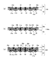
本発明の多層プリント配線板100は、図1(a)に示すように、第1配線層21aの一方の面に絶縁樹脂層11を介して第2配線層22a及びフィルドビア31が形成されたビルドアップ層20と、他方の面に第3配線層23a及びコンフォーマルビア32が形成されたビルドアップ層30とで構成されており、第1配線層21aと第2配線層22aとはフィルドビア31で、また第1配線層21aと第3配線層23aとはコンフォーマルビア32で、それぞれ電気的に接続されている。第1配線層21aに対してビルドアップ層20及びビルドアップ層30が対称に形成された対称構造の3層プリント配線板構造になっている。
【0021】
本発明の多層プリント配線板100aは、図1(b)に示すように、第1配線層21aの一方の面に絶縁樹脂層11を介して第2配線層22a、コンフォーマルビアランド22b及びコンフォーマルビア31aが形成されたビルドアップ層20aと、他方の面に第3配線層23a及びコンフォーマルビア32が形成されたビルドアップ層30とで構成されており、第1配線層21aと第2配線層22aとはコンフォーマルビア31aで、また第1配線層21aと第3配線層23aとはコンフォーマルビア32で、それぞれ電気的に接続されている。さらに、第1配線層21aに対してビルドアップ層20a及びビルドアップ層30が対称に形成された対称構造の3層プリント配線板構造になっている。
【0022】
また、本発明の多層プリント配線板200は、図1(c)に示すように、絶縁樹脂層11の両面に第1配線層21a、第2配線層22a及びフィルドビア31が形成された両面配線板40と、両面配線板40の一方の面に絶縁樹脂層13を介して第3配線層24a及びコンフォーマルビア33が形成されたビルドアップ層50と、他方の面に絶縁層14を介して第4配線層25a、ランド25b及びフィルドビア34が形成されたビルドアップ層60とで構成されており、第1配線層21aと第2配線層22aとはフィルドビア31で、第1配線層21aと第3配線層24aとはコンフォーマルビア33で、第2配線層22aと第4配線層25aとはフィルドビア34で、それぞれ電気的に接続されている。さらに、絶縁樹脂層11に対してビルドアップ層50及びビルドアップ層60が対称に形成された対称構造の4層プリント配線板構造になっている。
【0023】
上記本発明の多層プリント配線板100、100a及び200は、コア基板のないビルドアップ多層プリント配線板の構造とすることで、コア基板のBVH(ブラインドビアホール)による配線制約を取り除くことができるとともに、高密度化と薄型化が図れる。
具体的には、配線層のパターン設計自由度が増すとともに、配線層の収容性が向上し、薄型化及び微細配線層の形成が可能になり、高密度化が図れる。
また、対称構造のビルドアップ多層プリント配線板となっているため、薄型化しても配線板の反りが生じ難い。
【0024】
以下、本発明の半導体装置について説明する。
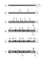
本発明の半導体装置300は、図2(a)に示すように、本発明の多層プリント配線板100上のフィルドビアと半導体80のパッド71が接合されて半導体80が搭載されており、半導体80と多層プリント配線板100の絶縁樹脂層との間にはアンダーフィル81樹脂を流し込んだ構造としている。
また、本発明の半導体装置400は、図2(b)に示すように、本発明の多層プリント配線板100a上のコンフォーマルビアランドと半導体80のパッド71が接合されて半導体80が搭載されており、半導体80と多層プリント配線板100aの絶縁樹脂層との間にはアンダーフィル81樹脂を流し込んだ構造としている。
【0025】
本発明の半導体装置500は、図2(c)に示すように、本発明の多層プリント配線板200上のフィルドビアまたランドと半導体80のパッド71が半田91を介して接合されて半導体80が搭載されており、半導体80と多層プリント配線板200の絶縁樹脂層との間にはアンダーフィル81樹脂を流し込んだ構造としている。
また、本発明の半導体装置600は、図2(d)に示すように、本発明の多層プリント配線板200上のフィルドビア34またはランド25bと半導体80のパッド71がバンプ92を介して接合されて半導体80が搭載されており、半導体80と多層プリント配線板200の絶縁樹脂層との間にはアンダーフィル81樹脂を流し込んだ構造としている。
【0026】
以下本発明に係る多層プリント配線板の製造方法について説明する
図3(a)〜(f)及び図4(g)〜(k)は、請求項5に係わる多層プリント配線板の製造方法の一実施例を工程順に示す模式構成断面図である。
まず、銅箔21上に、樹脂溶液を塗布するか、プリプレーグを積層して半硬化状態の絶縁樹脂層11を形成した片面銅箔付樹脂シート10を準備する(図3(a)参照)。
ここで、銅箔21は、12〜18μm厚のものが、絶縁層樹脂層11は、50〜100μm厚のものが、それぞれ使用される。さらに、片面銅箔付樹脂シート10に硫酸80〜160g/Lと35wt%過酸化水素90〜150g/Lを組成とする酸化性液を15〜60秒間スプレーすることにより、銅箔21をマクロエッチングして、5〜10μm厚の銅箔にする。これは、エッチング法で微細配線層を形成するための銅箔薄型化の一処方例である。
【0027】
次に、片面銅箔付樹脂シート10の絶縁樹脂層11の所定位置をレーザ加工してビア用孔41を形成し、デスミア、めっき触媒付与及び無電解銅めっきを行って、めっき下地層(特に、図示せず)を形成する(図3(b)参照)。
ここで、レーザ加工のレーザーとしては、炭酸ガスレーザ、エキシマレーザ、YAGレーザ等が利用でき、例えば、炭酸ガスレーザを使用した場合スポット径(直径)0.125mmのレーザビームを5〜20mJで1〜3パルス照射するのが好適である。
デスミア処方としては、例えば、MLB211:シプレイ・ファーイースト(株)製を20vol%、キューポジットZが10vol%からなる膨潤浴に60〜85℃で1〜5分間浸漬した後、MLB213A(シプレイ・ファーイースト(株)製)が10vol%とMLB213B(シプレイ・ファーイースト(株)製)が15vol%とからなるエッチング浴に55〜75℃で2〜10分間浸漬処理し、MLB216−2(シプレイ・ファーイースト(株)製)が20vol%からなる中和浴に35〜55℃で2〜10分間浸漬することにより、絶縁樹脂層11表面及びビア用孔41のデスミア処理を行う。
【0028】
また、めっき触媒付与及びめっき下地導電層の形成処方としては、例えば、上記基板をプレディップCP−3023(シプレイ・ファーイースト(株)製)浴に25℃で60秒間浸漬後、同社製キャタリスト同CP−3316浴に25℃で180秒間、同社製アクセラレーター(NR−2AとNR−2Bを各々10vol%と3vol%で混合した水溶液)に25℃で300秒間順次浸漬して、絶縁樹脂層11表面及びビア用孔41にパラジウム触媒を付与した後無電解銅めっきを行ってめっき下地導電層(特に、図示せず)を形成する。
【0029】
次に、銅箔21上に支持体シート61を貼着した後、感光性ドライフィルムを80〜120℃の熱ロールで絶縁樹脂層11上に貼着し、離型シートを剥離して絶縁樹脂層11上に感光層を形成し、超高圧水銀ランプで50〜200mJ/cm2の紫外線を照射してパターン露光した後、0.5〜2wt%炭酸ナトリウム水溶液をスプレー現像し、乾燥硬化してめっきレジストパターン51を形成する(図3(c)参照)。
ここで、支持体シート61は上記処理基板の補強及び処理工程での銅箔21の保護を行うためのもので、ポリエステルフィルム、ポリイミドフィルム、アミドフィルム、ポリプロピレンフィルム、ポリサルホンフィルム、ポリフェニルサルホンフィルム、ポリエーテルサルホンフィルム、ポフェニレンサルファイドフィルム、ポフェニレンエーテルフィルム、ポリエーテルエーテルケトンフィルム、ポフェニレンテレフタルアミドフィルムの中から工程処理条件等に合わせて適宜選択して使用する。
【0030】
次に、めっきレジストパターン51が形成された配線基板を硫酸銅めっき浴中に浸漬し、めっき下地導電層をカソードにして電解銅めっきを行い、絶縁樹脂層11上に10〜15μm厚の導体層22及びビア用孔41にフィルドビア31を形成する(図3(d)参照)。
ここで、電解銅めっき条件としては、例えば、硫酸銅70〜100g/L、硫酸150〜250g/L、塩酸50〜100ppmの組成から成る硫酸銅めっき浴を用いて、電流密度1.5〜2.5A/dm2の条件で20〜50分電解銅めっきを行って上記10〜15μm厚の銅からなる導体層を形成する。
また、ビア用孔41にはフィルドビアを形成したが特に限定されるものではなく、フィルドビア、コンフォーマルビアを適宜選択して用いれば良い。
【0031】
次に、0.5〜2wt%水酸化ナトリウム水溶液をスプレーして、めっきレジストパターン51を剥離処理し、めっきレジストパターン51下部にあっためっき下地導電層をフラッシュエッチングで除去し、支持体シート61を除去して第2配線層22aを形成し、銅箔21上に絶縁樹脂層11を介して第2配線層22a及びフィルドビア31が形成されたビルドアップ層20を形成する(図3(e)参照)。
【0032】
次に、第2配線層22a側に支持体シート62を貼着した後感光性のドライフィルムを80〜120℃の熱ロールで絶縁樹脂層11上に貼着し、離型シートを剥離して、絶縁樹脂層11上に感光層を形成し、超高圧水銀ランプで50〜200mJ/cm2の紫外線を照射してパターン露光した後、0.5〜2wt%炭酸ナトリウム水溶液をスプレー現像し、乾燥硬化してレジストパターン52を形成する(図3(f)参照)。
ここで、支持体シート62は上記処理基板の補強及び処理工程での銅箔21の保護を行うためのもので、ポリエステルフィルム、ポリイミドフィルム、アミドフィルム、ポリプロピレンフィルム、ポリサルホンフィルム、ポリフェニルサルホンフィルム、ポリエーテルサルホンフィルム、ポフェニレンサルファイドフィルム、ポフェニレンエーテルフィルム、ポリエーテルエーテルケトンフィルム、ポフェニレンテレフタルアミドフィルムの中から工程処理条件等に合わせて適宜選択して使用する。
【0033】
次に、レジストパターン52をマスクにして塩化第二銅200〜400g/l、塩酸100〜150g/lからなるエッチング液をスプレーして銅箔21をエッチング除去し、レジストパターン52を0.5〜2.0wt%の水酸化ナトリウム水溶液で剥離除去して、第1配線層21aを形成する(図4(g)参照)。
【0034】
次に、第1配線層21a上に樹脂溶液を塗布するか、もしくはプリプレーグシート等を貼着するかの方法で、絶縁樹脂層12を形成し、絶縁樹脂層12の所定の位置にレーザー加工等によりビア用孔42を形成し、上記図3(b)と同じ処方で、デスミア、めっき触媒付与及び無電解銅めっきを行ってめっき下地導電層(特に、図示せず)形成する(図4(h)参照)。
【0035】
次に、感光性のドライフィルムを80〜120℃の熱ロールで絶縁樹脂層12上に貼着し、離型シートを剥離して絶縁樹脂層12上に感光層を形成し、超高圧水銀ランプで50〜200mJ/cm2の紫外線を照射してパターン露光した後、0.5〜2wt%炭酸ナトリウム水溶液をスプレー現像し、乾燥硬化してめっきレジストパターン53を形成する(図4(i)参照)。
【0036】
次に、めっきレジストパターン53が形成された配線基板を硫酸銅めっき浴中に浸漬し、めっき下地導電層をカソードにして電解銅めっきを行い、絶縁樹脂層11上に10〜15μm厚の導体層23及びビア用孔42にコンフォーマルビア32を形成する(図4(j)参照)。
ここで、電解銅めっき条件としては、上記図3(d)の工程に用いた条件と同じ処方で良い。
また、ビア用孔42にはコンフォーマルビアを形成したが特に限定されるものではなく、コンフォーマルビア、フィルドビアを適宜選択して用いれば良い。
【0037】
次に、めっきレジストパターン53を0.5〜2.0wt%水酸化ナトリウム水溶液で剥離除去し、めっきレジストパターン53下部にあっためっき下地導電層をフラッシュエッチングで除去して第3配線層23aを形成し、支持体シート62を除去して、第1配線層21aの一方の面に絶縁樹脂層11を介して第2配線層22a及びフィルドビア31が形成されたビルドアップ層20、他方の面に絶縁樹脂層12を介して第3配線層23a及びコンフォーマルビア32が形成されたビルドアップ層30からなる3層プリント配線板100を得る(図4(k)参照)。
さらに、必要に応じて上記絶縁樹脂層、配線層及びコンフォーマルビアもしくはフィルドビア形成工程を必要回数繰り返すことにより、所望の多層プリント配線板を得ることができる。
【0038】
図5(a)〜(f)及び図6(g)〜(k)は、請求項6に係わる多層プリント配線板の製造方法の一実施例を工程順に示す模式構成断面図である。
まず、図5(a)〜(f)の工程は、上記図3(a)〜(f)と同様の工程で処理し、第1配線層21a、第2配線層22a、ランド22c及びフィルドビア32を形成し、絶縁樹脂層11の両面に第1配線層21aと第2配線層22aランド22b及びフィルドビア32が形成された両面配線板40を得る(図6(g)参照)。
【0039】
次に、両面配線板40の両面にプリプレーグシートを積層して絶縁樹脂層13及び絶縁樹脂層14を形成し、絶縁樹脂層13及び絶縁樹脂層14の所定の位置にレーザー加工等によりビア用孔43及びビア用孔44を形成し、デスミア、めっき触媒付与及び無電解銅めっきを行ってめっき下地導電層(特に、図示せず)形成する(図6(h)参照)。
ここで、デスミア、めっき触媒付与及び無電解銅めっき条件としては、上記図3(b)の工程に用いた条件と同じ処方で良い。
【0040】
次に、感光性ドライフィルムを80〜120℃の熱ロールで絶縁樹脂層13及び絶縁樹脂層14上に貼着し、離型シートを剥離して絶縁樹脂層13及び絶縁樹脂層14上に感光層を形成し、超高圧水銀ランプで50〜200mJ/cm2の紫外線を両面照射してパターン露光した後、0.5〜2wt%炭酸ナトリウム水溶液をスプレー現像し、乾燥硬化してめっきレジストパターン54及びめっきレジストパターン55をそれぞれ形成する(図6(i)参照)。
【0041】
次に、めっきレジストパターン54及びめっきレジストパターン55が形成された配線基板を硫酸銅めっき浴中に浸漬し、めっき下地導電層をカソードにして電解銅めっきを行い、絶縁樹脂層13上に10〜15μm厚の導体層24及びビア用孔43にコンフォーマルビア33を、絶縁樹脂層14上に10〜15μm厚の導体層25及びビア用孔44にフィルドビア34をそれぞれ形成する(図6(j)参照)。
ここで、電解銅めっき条件としては、上記図3(d)の工程に用いた条件と同じ処方で良い。
【0042】
次に、めっきレジストパターン54及びめっきレジストパターン55を0.5〜2.0wt%水酸化ナトリウム水溶液で剥離除去し、めっきレジストパターン54及びめっきレジストパターン55下部にあっためっき下地導電層をフラッシュエッチングで除去して、第3配線層24a、第4配線層25a及びランド25bを形成し、両面配線板40の一方の面に絶縁樹脂層13を介して第3配線層24a及びコンフォーマルビア33が形成されたビルドアップ層50、他方の面に絶縁樹脂層13を介して第4配線層25a及びフィルドビア34が形成されたビルドアップ層50をそれぞれ形成し、4層プリント配線板200を得る(図6(k)参照)。
さらに、必要に応じて上記絶縁樹脂層、配線層及びコンフォーマルビアもしくはフィルドビア形成工程を必要回数繰り返すことにより、所望の多層プリント配線板を得ることができる。
【0043】
【発明の効果】
上記したように、本発明の多層プリント配線板は、コア基板のないビルドアップ多層プリント配線板の構造とすることで、配線層のパターン設計自由度が増すとともに、配線層の収容性が向上し、薄型化及び微細配線層の形成が可能になり、高密度化が図れる。
また、対称構造のビルドアップ多層プリント配線板となっているため、薄型化しても配線板の反りが生じ難い。
また、本発明の多層プリント配線板の製造方法では、セミアディティブ法を用いて配線層を形成しているので、微細パターンの配線層を容易に得ることができる。
また、支持体シートを用いているので、多層プリント配線板の製造工程中での保護層を兼ねた処理基板の補強を容易に実施でき、特に、薄型化した配線板を製造する場合には変形防止効果が発揮される。
【図面の簡単な説明】
【図1】(a)〜(c)は、本発明の多層プリント配線板の一実施例を示す模式構成断面図である。
【図2】(a)〜(d)は、本発明の半導体装置の一実施例を示す模式構成断面図である。
【図3】(a)及び(f)は、本発明の請求項5に係る多層プリント配線板の製造法における工程の一部を模式的に示す断面図である。
【図4】(g)及び(k)は、本発明の請求項5に係る多層プリント配線板の製造法における工程の一部を模式的に示す断面図である。
【図5】(a)及び(f)は、本発明の請求項6に係る多層プリント配線板の製造法における工程の一部を模式的に示す断面図である。
【図6】(g)及び(k)は、本発明の請求項6に係る多層プリント配線板の製造法における工程の一部を模式的に示す断面図である。
【図7】(a)及び(f)は、従来の多層プリント配線板の製造法の工程一例を模式的に示す断面図である。
【図8】(a)及び(d)は、従来の多層プリント配線板の製造法の工程一例を模式的に示す断面図である。
【符号の説明】
10……片面銅箔付樹脂シート
11、12、13、14、111、114……絶縁樹脂層
20、20a、30、50、60、730、740、830……ビルドアップ層
21、121、122、125、126……銅箔
21a……第1配線層
22、23、24、25……導体層
22a……第2配線層
22b……コンフォーマルビアランド
22c、25b……ランド
23a、24a……第3配線層
25a……第4配線層
31、34……フィルドビア
31a、32、33、131、134、135……コンフォーマルビア
40……両面配線板
41、42、43、44、141、142……ビア用孔
51、53、54、55、151……めっきレジストパターン
52、153……レジストパターン
61、62……支持体シート
71……パッド
80……半導体
81……アンダーフィル
91……半田
92……バンプ
100、100a、200、700、800……多層プリント配線板
121a、122a、125a、126a、127、128、129……配線層
152、154……保護マスク層
300、400、500、600……半導体装置
710、810……両面銅貼り積層板
720、820……コア基板[0001]
TECHNICAL FIELD OF THE INVENTION
The present invention relates to a multilayer printed wiring board having a plurality of wiring layers formed on both surfaces of a first wiring layer via insulating layers, a method for manufacturing the same, and a semiconductor device.
[0002]
[Prior art]
In recent years, a multilayer printed wiring board having a high-density and high-precision wiring layer has been required for a printed wiring board on which a semiconductor device is mounted due to the development of semiconductor mounting technology. In order to form high-density, high-precision wiring layers, printed wiring boards are multilayered, the line width of the wiring layers is also reduced, and via holes used for connection between wiring layers are required to have smaller hole diameters. ing. In addition, high-precision processing is also required for the processing of via-holes so as to minimize displacement. In order to satisfy such requirements, a so-called build-up method has been put to practical use, in which wiring layers and insulating layers are alternately formed to form a multilayer wiring layer to produce a multilayer printed wiring board.
[0003]
FIGS. 7A to 7F show an example of a conventional technique for producing a multilayer printed wiring board by a build-up method (for example, see Patent Document 1).
Hereinafter, a method for manufacturing a multilayer printed wiring board by a build-up method will be described with reference to FIGS.
First, a double-sided copper-clad laminate 710 in which
Next, the
[0004]
Next, a photosensitive layer is formed by laminating a photosensitive dry film on both sides, and a series of patterning processes such as pattern exposure and development are performed on the photosensitive layer on the
[0005]
Next, a photosensitive dry film is laminated on both sides to form a photosensitive layer, and the photosensitive layer on the
[0006]
Next, the
Further, build-up layers 730 and 740 are formed on both surfaces of the core substrate 720 to obtain a four-layer printed wiring board 700 (see FIG. 7F).
[0007]
FIGS. 8A to 8D show another example of a conventional technique for manufacturing a multilayer printed wiring board by a build-up method (for example, see Patent Document 2).
Hereinafter, a method of manufacturing a multilayer printed wiring board by a build-up method will be described with reference to FIGS.
First, a double-sided copper-clad laminate 810 in which
Next, a predetermined position on the
[0008]
Next, the
[0009]
Next, the
[0010]
[Patent Document 1]
JP 2001-94252 A
[Patent Document 2]
JP 09-46042 A
[0011]
[Problems to be solved by the invention]
In the method of manufacturing a multilayer printed wiring board by a build-up method using the above-described conventional technique, it is difficult to form a fine wiring layer because a subtractive method is used.
Further, the multilayer printed wiring board manufactured using the technique of
[0012]
The present invention has been devised in view of the above problems, and has as its object to provide a method of manufacturing a multilayer printed wiring board on which a fine wiring layer can be formed, a multilayer printed wiring board that is unlikely to warp, and a semiconductor device.
[0013]
[Means for Solving the Problems]
In order to achieve the above object in the present invention, first, according to
[0014]
According to a second aspect of the present invention, the first wiring layer is electrically connected to the wiring layer and the wiring layer by a conformal via or a filled via via the insulating resin layer. A multilayer printed wiring board as described in 1 above.
[0015]
According to a third aspect of the present invention, the multilayer printed wiring board according to the first or second aspect is a multilayer printed wiring board having a symmetric structure.
[0016]
A semiconductor device comprising a semiconductor mounted on the multilayer printed wiring board according to any one of
[0017]
The method for manufacturing a multilayer printed wiring board according to any one of
(A) A step of preparing a
(B) A step of forming a via
(C) A step of forming a plating resist
(D) A step of forming a
(E) The resist
(F) A step of forming a resist
(G) a step of etching the
(H) An insulating
(I) a step of forming a photosensitive layer on the insulating
(J) A step of performing electrolytic copper plating using the plating underlying conductive layer as a cathode to form a
(K) The resist
(L) a step of repeating the insulating resin layer, the wiring layer, and the conformal via or filled via forming step a required number of times;
[0018]
The method for manufacturing a multilayer printed wiring board according to any one of
(A) A step of preparing a
(B) A step of forming a via
(C) A step of forming a plating resist
(D) A step of forming a
(E) The plating resist
(F) A step of forming a resist
(G) A step of etching the
(H) An insulating
(I) A step of forming a photosensitive layer on the insulating
(J) A step of forming a
(K) The plating resist
(L) a step of repeating the insulating resin layer, the wiring layer, and the conformal via or filled via forming step a required number of times;
[0019]
7. The method according to
[0020]
BEST MODE FOR CARRYING OUT THE INVENTION
Hereinafter, embodiments of the present invention will be described.
One embodiment of the multilayer printed wiring board of the present invention is shown in FIGS. 1 (a), 1 (b) and 1 (c). FIGS. 2A to 2D show an embodiment of a semiconductor device in which a semiconductor is mounted on a multilayer printed wiring board according to the present invention.
As shown in FIG. 1A, a multilayer printed
[0021]
As shown in FIG. 1B, the multilayer printed
[0022]
Further, as shown in FIG. 1C, the multilayer printed
[0023]
The multilayer printed
More specifically, the degree of freedom in pattern design of the wiring layer is increased, the accommodating property of the wiring layer is improved, the thickness can be reduced and the fine wiring layer can be formed, and the density can be increased.
In addition, since it is a build-up multilayer printed wiring board having a symmetric structure, the wiring board is unlikely to be warped even if it is made thin.
[0024]
Hereinafter, the semiconductor device of the present invention will be described.
As shown in FIG. 2A, the
Further, as shown in FIG. 2B, the
[0025]
In the
Further, as shown in FIG. 2D, the
[0026]
Hereinafter, a method for manufacturing a multilayer printed wiring board according to the present invention will be described.
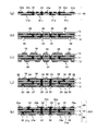
3 (a) to 3 (f) and 4 (g) to 4 (k) are schematic sectional views showing one embodiment of a method for manufacturing a multilayer printed wiring board according to
First, a
Here, a
[0027]
Next, a predetermined position of the insulating
Here, as a laser for laser processing, a carbon dioxide gas laser, an excimer laser, a YAG laser, or the like can be used. For example, when a carbon dioxide gas laser is used, a laser beam having a spot diameter (diameter) of 0.125 mm is applied at 5 to 20 mJ at 1 to 3 mJ. It is preferable to perform pulse irradiation.
As a desmear formulation, for example, MLB211: manufactured by Shipley Far East Co., Ltd. is immersed in a swelling bath consisting of 20 vol% and 10 cup% Z at 60 to 85 ° C. for 1 to 5 minutes. Yeast Co., Ltd.) is immersed in an etching bath consisting of 10 vol% and MLB213B (manufactured by Shipley Fur East Co., Ltd.) at 15 vol% at 55 to 75 ° C. for 2 to 10 minutes, and MLB216-2 (Shipley Fur Co., Ltd.) The surface of the insulating
[0028]
In addition, as a prescription for applying a plating catalyst and forming a conductive layer under the plating, for example, after dipping the above substrate in a bath of Predip CP-3023 (manufactured by Shipley Far East Co., Ltd.) at 25 ° C. for 60 seconds, a catalyst manufactured by the company is used. In the same CP-3316 bath at 25 ° C. for 180 seconds, the film was sequentially immersed in an accelerator (an aqueous solution in which NR-2A and NR-2B were mixed at 10 vol% and 3 vol%, respectively) at 25 ° C. for 300 seconds at 25 ° C. to form an insulating resin layer. After applying a palladium catalyst to the
[0029]
Next, after attaching the
Here, the
[0030]
Next, the wiring board on which the plating resist
Here, the electrolytic copper plating conditions are, for example, a copper sulfate plating bath having a composition of copper sulfate 70 to 100 g / L, sulfuric acid 150 to 250 g / L,
Although a filled via is formed in the via
[0031]
Next, the plating resist
[0032]
Next, after attaching the
Here, the
[0033]
Next, using the resist
[0034]
Next, the insulating
[0035]
Next, a photosensitive dry film is stuck on the insulating
[0036]
Next, the wiring board on which the plating resist
Here, the conditions for electrolytic copper plating may be the same as the conditions used in the step of FIG.
Further, a conformal via is formed in the via
[0037]
Next, the plating resist
Further, if necessary, the steps of forming the insulating resin layer, the wiring layer, and the conformal via or filled via are repeated a required number of times, whereby a desired multilayer printed wiring board can be obtained.
[0038]
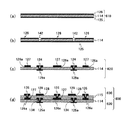
5 (a) to 5 (f) and 6 (g) to 6 (k) are schematic sectional views showing one embodiment of a method for manufacturing a multilayer printed wiring board according to claim 6 in the order of steps.
First, in the steps of FIGS. 5A to 5F, processing is performed in the same steps as in FIGS. 3A to 3F, and the
[0039]
Next, a prepreg sheet is laminated on both sides of the double-
The desmear, plating catalyst application, and electroless copper plating conditions may be the same as the conditions used in the step of FIG. 3B.
[0040]
Next, a photosensitive dry film is stuck on the insulating
[0041]
Next, the plating resist
Here, the conditions for electrolytic copper plating may be the same as the conditions used in the step of FIG.
[0042]
Next, the plating resist
Further, if necessary, the steps of forming the insulating resin layer, the wiring layer, and the conformal via or filled via are repeated a required number of times, whereby a desired multilayer printed wiring board can be obtained.
[0043]
【The invention's effect】
As described above, the multilayer printed wiring board of the present invention has a structure of a build-up multilayer printed wiring board without a core substrate, thereby increasing the degree of freedom in pattern design of the wiring layer and improving the accommodation of the wiring layer. In addition, the thickness can be reduced and the fine wiring layer can be formed, and the density can be increased.
In addition, since it is a build-up multilayer printed wiring board having a symmetric structure, the wiring board is unlikely to be warped even if it is made thin.
In the method for manufacturing a multilayer printed wiring board according to the present invention, since the wiring layer is formed using the semi-additive method, a wiring layer having a fine pattern can be easily obtained.
In addition, since the support sheet is used, it is possible to easily reinforce the processing substrate also serving as a protective layer during the manufacturing process of the multilayer printed wiring board. The prevention effect is exhibited.
[Brief description of the drawings]
FIGS. 1A to 1C are schematic sectional views showing one embodiment of a multilayer printed wiring board according to the present invention.
FIGS. 2A to 2D are schematic sectional views showing one embodiment of the semiconductor device of the present invention.
3 (a) and 3 (f) are cross-sectional views schematically showing some of the steps in the method for manufacturing a multilayer printed wiring board according to
4 (g) and 4 (k) are cross-sectional views schematically showing some of the steps in the method for manufacturing a multilayer printed wiring board according to
FIGS. 5A and 5F are cross-sectional views schematically showing some of the steps in the method for manufacturing a multilayer printed wiring board according to claim 6 of the present invention.
6 (g) and 6 (k) are cross-sectional views schematically showing some of the steps in the method for manufacturing a multilayer printed wiring board according to claim 6 of the present invention.
FIGS. 7A and 7F are cross-sectional views schematically showing an example of steps of a conventional method for manufacturing a multilayer printed wiring board.
FIGS. 8A and 8D are cross-sectional views schematically showing an example of steps of a conventional method for manufacturing a multilayer printed wiring board.
[Explanation of symbols]
10 ... Resin sheet with copper foil on one side
11, 12, 13, 14, 111, 114 ... Insulating resin layer
20, 20a, 30, 50, 60, 730, 740, 830... Build-up layer
21, 121, 122, 125, 126 ... copper foil
21a... First wiring layer
22, 23, 24, 25 ... conductor layer
22a... Second wiring layer
22b ... Conformal Vialand
22c, 25b ... land
23a, 24a... Third wiring layer
25a... Fourth wiring layer
31, 34 ... filled via
31a, 32, 33, 131, 134, 135 ... conformal via
40 Double-sided wiring board
41, 42, 43, 44, 141, 142 ... Via holes
51, 53, 54, 55, 151 ... Plating resist pattern
52, 153 resist pattern
61, 62 ... Support sheet
71 ... Pad
80 ... Semiconductor
81 …… Underfill
91 …… Solder
92 ...... Bump
100, 100a, 200, 700, 800 ... multilayer printed wiring board
121a, 122a, 125a, 126a, 127, 128, 129 ... wiring layer
152, 154: Protective mask layer
300, 400, 500, 600 ... semiconductor device
710, 810: double-sided copper-clad laminate
720, 820 ... core substrate
Claims (7)
(a)絶縁樹脂層(11)及び銅箔(21)からなる片面銅箔付樹脂シート(10)を準備する工程。
(b)片面銅箔付樹脂シート(10)の絶縁樹脂層(11)の所定位置にビア用孔(41)を形成し、デスミア、めっき触媒付与及び無電解銅めっきを行って、めっき下地導電層を形成する工程。
(c)銅箔(21)上に支持体シート(61)を貼着した後めっき下地導電層上に感光層を形成し、パターン露光、現像等の一連のパターニング処理を行ってめっきレジストパターン(51)を形成する工程。
(d)めっき下地導電層をカソードにして電解銅めっきを行って所定厚の導体層(22)及びフィルドビア(31)を形成する工程。
(e)レジストパターン(51)を剥離処理し、めっきレジストパターン(51)下部にあっためっき下地導電層をフラッシュエッチングにて除去し、第2配線層(22a)及びフィルドビア(31)を形成し、支持体シート(61)を除去する工程。
(f)第2配線層(22a)側に支持体シート(62)を貼着した後銅箔(21)上に感光層を形成し、パターン露光、現像等の一連のパターニング処理を行ってレジストパターン(52)を形成する工程。
(g)レジストパターン(52)をマスクにして銅箔(21)をエッチング処理し、レジストパターン(52)を剥離処理して、第1配線層(21a)を形成する工程。
(h)第1配線層(21a)側に所定厚の絶縁樹脂層(12)を形成し、絶縁樹脂層(12)の所定位置にレーザー加工等によりビア用孔(42)を形成し、デスミア、めっき触媒付与及び無電解銅めっきを行って、めっき下地導電層を形成する工程。
(i)絶縁樹脂層(12)側に感光層を形成し、パターン露光、現像等の一連のパターニング処理を行ってめっきレジストパターン(53)を形成する工程。
(j)めっき下地導電層をカソードにして電解銅めっきを行い、所定厚の導体層(23)及びコンフォーマルビア(32)を形成する工程。
(k)レジストパターン(53)を剥離処理し、めっきレジストパターン(53)下部にあっためっき下地導電層をフラッシュエッチングにて除去し、第3配線層(23a)及びコンフォーマルビア(32)を形成し、支持体シート(62)を除去する工程。
(l)上記絶縁樹脂層、配線層及びコンフォーマルビアもしくはフィルドビア形成工程を必要回数繰り返す工程。The method for manufacturing a multilayer printed wiring board according to any one of claims 1 to 3, further comprising at least the following steps.
(A) a step of preparing a resin sheet (10) with a single-sided copper foil comprising an insulating resin layer (11) and a copper foil (21);
(B) A via hole (41) is formed at a predetermined position of the insulating resin layer (11) of the resin sheet (10) with a single-sided copper foil, and desmearing, plating catalyst application and electroless copper plating are performed, and plating base conductive is formed. Forming a layer;
(C) After affixing the support sheet (61) on the copper foil (21), a photosensitive layer is formed on the plating underlying conductive layer, and a series of patterning processes such as pattern exposure and development are performed to perform plating resist pattern ( Step 51).
(D) A step of forming a conductor layer (22) and a filled via (31) having a predetermined thickness by performing electrolytic copper plating using the plating underlying conductive layer as a cathode.
(E) The resist pattern (51) is peeled off, and the underlying conductive layer under the plating resist pattern (51) is removed by flash etching to form a second wiring layer (22a) and a filled via (31). Removing the support sheet (61).
(F) After attaching the support sheet (62) to the second wiring layer (22a) side, a photosensitive layer is formed on the copper foil (21), and a series of patterning processes such as pattern exposure and development are performed to form a resist. Forming a pattern (52);
(G) a step of etching the copper foil (21) using the resist pattern (52) as a mask and removing the resist pattern (52) to form a first wiring layer (21a);
(H) An insulating resin layer (12) having a predetermined thickness is formed on the first wiring layer (21a) side, and a via hole (42) is formed at a predetermined position of the insulating resin layer (12) by laser processing or the like. Forming a plating base conductive layer by applying a plating catalyst and performing electroless copper plating.
(I) forming a photosensitive layer on the insulating resin layer (12) side and performing a series of patterning processes such as pattern exposure and development to form a plating resist pattern (53);
(J) a step of forming a conductive layer (23) and a conformal via (32) having a predetermined thickness by performing electrolytic copper plating using the plating base conductive layer as a cathode;
(K) The resist pattern (53) is peeled off, the underlying plating conductive layer under the plating resist pattern (53) is removed by flash etching, and the third wiring layer (23a) and the conformal via (32) are removed. Forming and removing the support sheet (62).
(L) a step of repeating the insulating resin layer, the wiring layer, and the conformal via or filled via forming step a required number of times;
(a)絶縁樹脂層(11)及び銅箔(21)からなる片面銅箔付樹脂シート(10)を準備する工程。
(b)絶縁樹脂層(11)の所定位置にビア用孔(41)を形成し、デスミア、めっき触媒付与及び無電解銅めっきを行って、めっき下地導電層を形成する工程。
(c)銅箔(21)上に支持体シート(61)を貼着した後めっき下地導電層上に感光層を形成し、パターン露光、現像等の一連のパターニング処理を行ってめっきレジストパターン(51)を形成する工程。
(d)めっき下地導電層をカソードにして電解銅めっきを行い、所定厚の導体層(22)及びフィルドビア(31)を形成する工程。
(e)めっきレジストパターン(51)を剥離処理し、めっきレジストパターン(51)下部にあっためっき下地導電層をフラッシュエッチングにて除去し、第2配線層(22a)及びフィルドビア(31)を形成し、支持体シート(61)を除去する工程。
(f)第2配線層(22a)側に支持体シート(62)を貼着した後銅箔(21)上に感光層を形成し、パターン露光、現像等の一連のパターニング処理を行ってレジストパターン(52)を形成する工程。
(g)レジストパターン(52)をマスクにして銅箔(21)をエッチング処理し、レジストパターン(52)を除去して第1配線層(21a)を形成し、支持体シート(62)を除去する工程。
(h)第1配線層(21a)及び第2配線層(22a)側にそれぞれ所定厚の絶縁樹脂層(13)及び絶縁樹脂層(14)を形成し、絶縁樹脂層(13)及び絶縁樹脂層(14)の所定位置にレーザー加工等によりそれぞれビア用孔(43)及びビア用孔(44)を形成し、デスミア、めっき触媒付与及び無電解銅めっきを行って、めっき下地導電層をそれぞれ形成する工程。
(i)絶縁樹脂層(13)及び絶縁樹脂層(14)側にそれぞれ感光層を形成し、パターン露光、現像等の一連のパターニング処理を行ってめっきレジストパターン(54)及びめっきレジストパターン(55)を形成する工程。
(j)めっき下地導電層をカソードにして電解銅めっきを行い、所定厚の導体層(24)及びコンフォーマルビア(33)、導体層(25)及びフィルドビア(34)をそれぞれ形成する工程。
(k)めっきレジストパターン(54)及(55)を剥離処理し、めっきレジストパターン(54)及び(55)下部にあっためっき下地導電層をフラッシュエッチングにて除去し、第3配線層(24a)及びコンフォーマルビア(33)、第4配線層(25a)及びフィルドビア(34)を形成する工程。
(l)上記絶縁樹脂層、配線層及びコンフォーマルビアもしくはフィルドビア形成工程を必要回数繰り返す工程。The method for manufacturing a multilayer printed wiring board according to any one of claims 1 to 3, further comprising at least the following steps.
(A) a step of preparing a resin sheet (10) with a single-sided copper foil comprising an insulating resin layer (11) and a copper foil (21);
(B) A step of forming a via hole (41) at a predetermined position of the insulating resin layer (11), performing desmearing, applying a plating catalyst, and performing electroless copper plating to form a plating underlying conductive layer.
(C) After affixing the support sheet (61) on the copper foil (21), a photosensitive layer is formed on the plating underlying conductive layer, and a series of patterning processes such as pattern exposure and development are performed to perform plating resist pattern ( Step 51).
(D) A step of forming a conductor layer (22) and a filled via (31) having a predetermined thickness by performing electrolytic copper plating using the plating base conductive layer as a cathode.
(E) The plating resist pattern (51) is peeled off, and the underlying conductive layer under the plating resist pattern (51) is removed by flash etching to form a second wiring layer (22a) and a filled via (31). And removing the support sheet (61).
(F) After attaching the support sheet (62) to the second wiring layer (22a) side, a photosensitive layer is formed on the copper foil (21), and a series of patterning processes such as pattern exposure and development are performed to form a resist. Forming a pattern (52);
(G) The copper foil (21) is etched using the resist pattern (52) as a mask, the resist pattern (52) is removed to form a first wiring layer (21a), and the support sheet (62) is removed. Process.
(H) forming an insulating resin layer (13) and an insulating resin layer (14) having a predetermined thickness on the first wiring layer (21a) and the second wiring layer (22a) side, respectively; Via holes (43) and via holes (44) are respectively formed at predetermined positions of the layer (14) by laser processing or the like, and desmearing, plating catalyst application, and electroless copper plating are performed to form a plating underlying conductive layer, respectively. Forming step.
(I) A photosensitive layer is formed on each of the insulating resin layer (13) and the insulating resin layer (14), and a series of patterning processes such as pattern exposure and development are performed to perform a plating resist pattern (54) and a plating resist pattern (55). ).
(J) a step of performing electrolytic copper plating using the plating base conductive layer as a cathode to form a conductor layer (24) and a conformal via (33), a conductor layer (25), and a filled via (34) each having a predetermined thickness.
(K) The plating resist patterns (54) and (55) are peeled off, the underlying plating conductive layer under the plating resist patterns (54) and (55) is removed by flash etching, and the third wiring layer (24a) is removed. And forming a conformal via (33), a fourth wiring layer (25a), and a filled via (34).
(L) a step of repeating the insulating resin layer, the wiring layer, and the conformal via or filled via forming step a required number of times;
Priority Applications (1)
| Application Number | Priority Date | Filing Date | Title |
|---|---|---|---|
| JP2003052445A JP4066848B2 (en) | 2003-02-28 | 2003-02-28 | Manufacturing method of multilayer printed wiring board |
Applications Claiming Priority (1)
| Application Number | Priority Date | Filing Date | Title |
|---|---|---|---|
| JP2003052445A JP4066848B2 (en) | 2003-02-28 | 2003-02-28 | Manufacturing method of multilayer printed wiring board |
Publications (2)
| Publication Number | Publication Date |
|---|---|
| JP2004265967A true JP2004265967A (en) | 2004-09-24 |
| JP4066848B2 JP4066848B2 (en) | 2008-03-26 |
Family
ID=33117317
Family Applications (1)
| Application Number | Title | Priority Date | Filing Date |
|---|---|---|---|
| JP2003052445A Expired - Fee Related JP4066848B2 (en) | 2003-02-28 | 2003-02-28 | Manufacturing method of multilayer printed wiring board |
Country Status (1)
| Country | Link |
|---|---|
| JP (1) | JP4066848B2 (en) |
Cited By (12)
| Publication number | Priority date | Publication date | Assignee | Title |
|---|---|---|---|---|
| JP2006245122A (en) * | 2005-03-01 | 2006-09-14 | Dainippon Printing Co Ltd | Wiring member and method of manufacturing wiring member |
| JP2006294692A (en) * | 2005-04-06 | 2006-10-26 | Nec Electronics Corp | Semiconductor device and its manufacturing method |
| JP2007035825A (en) * | 2005-07-26 | 2007-02-08 | Nec Electronics Corp | Semiconductor device and its manufacturing method |
| JP2007149731A (en) * | 2005-11-24 | 2007-06-14 | Shinko Electric Ind Co Ltd | Wiring board, semiconductor device, and process for producing wiring board |
| JP2009164557A (en) * | 2008-01-03 | 2009-07-23 | Samsung Electro-Mechanics Co Ltd | Printed circuit board and method of manufacturing the same |
| US7928001B2 (en) * | 2006-10-02 | 2011-04-19 | Renesas Electronics Corporation | Electronic device and method of manufacturing the same |
| US8027169B2 (en) | 2005-11-02 | 2011-09-27 | Ibiden Co., Ltd. | Multilayer printed wiring board for semiconductor devices and method for manufacturing the board |
| JP2012060159A (en) * | 2011-12-05 | 2012-03-22 | Shinko Electric Ind Co Ltd | Wiring board, semiconductor device and wiring board manufacturing method |
| US8237056B2 (en) | 2008-11-12 | 2012-08-07 | Ibiden Co., Ltd. | Printed wiring board having a stiffener |
| US9078344B2 (en) | 2011-11-23 | 2015-07-07 | Samsung Electro-Mechanics Co., Ltd. | Printed circuit board and manufacturing method thereof |
| JP2016134395A (en) * | 2015-01-15 | 2016-07-25 | イビデン株式会社 | Manufacturing method of printed wiring board |
| WO2022113968A1 (en) * | 2020-11-27 | 2022-06-02 | 京セラ株式会社 | Printed wiring board and method for manufacturing printed wiring board |
-
2003
- 2003-02-28 JP JP2003052445A patent/JP4066848B2/en not_active Expired - Fee Related
Cited By (22)
| Publication number | Priority date | Publication date | Assignee | Title |
|---|---|---|---|---|
| JP4620495B2 (en) * | 2005-03-01 | 2011-01-26 | 大日本印刷株式会社 | Flexures and methods of manufacturing flexures |
| JP2006245122A (en) * | 2005-03-01 | 2006-09-14 | Dainippon Printing Co Ltd | Wiring member and method of manufacturing wiring member |
| US8035231B2 (en) | 2005-04-06 | 2011-10-11 | Renesas Electronics Corporation | Semiconductor device and method of manufacturing the same |
| US7927999B2 (en) | 2005-04-06 | 2011-04-19 | Renesas Electronics Corporation | Method of forming metal interconnect layers for flip chip device |
| JP2006294692A (en) * | 2005-04-06 | 2006-10-26 | Nec Electronics Corp | Semiconductor device and its manufacturing method |
| JP2007035825A (en) * | 2005-07-26 | 2007-02-08 | Nec Electronics Corp | Semiconductor device and its manufacturing method |
| US8058165B2 (en) | 2005-07-26 | 2011-11-15 | Renesas Electronics Corporation | Semiconductor device and method of manufacturing the same |
| JP2012039139A (en) * | 2005-11-02 | 2012-02-23 | Ibiden Co Ltd | Multilayer printed wiring board |
| US8624121B2 (en) | 2005-11-02 | 2014-01-07 | Ibiden Co., Ltd. | Multilayer printed wiring board for semiconductor devices and method for manufacturing the board |
| JP5105168B2 (en) * | 2005-11-02 | 2012-12-19 | イビデン株式会社 | Multilayer printed wiring board |
| US8027169B2 (en) | 2005-11-02 | 2011-09-27 | Ibiden Co., Ltd. | Multilayer printed wiring board for semiconductor devices and method for manufacturing the board |
| US8085546B2 (en) | 2005-11-02 | 2011-12-27 | Ibiden Co., Ltd. | Multilayer printed wiring board for semiconductor devices and method for manufacturing the board |
| JP2007149731A (en) * | 2005-11-24 | 2007-06-14 | Shinko Electric Ind Co Ltd | Wiring board, semiconductor device, and process for producing wiring board |
| US7928001B2 (en) * | 2006-10-02 | 2011-04-19 | Renesas Electronics Corporation | Electronic device and method of manufacturing the same |
| US8181339B2 (en) | 2008-01-03 | 2012-05-22 | Samsung Electro-Mechanics Co., Ltd. | Method of manufacturing a printed circuit board |
| JP4721196B2 (en) * | 2008-01-03 | 2011-07-13 | サムソン エレクトロ−メカニックス カンパニーリミテッド. | Method for manufacturing printed circuit board |
| JP2009164557A (en) * | 2008-01-03 | 2009-07-23 | Samsung Electro-Mechanics Co Ltd | Printed circuit board and method of manufacturing the same |
| US8237056B2 (en) | 2008-11-12 | 2012-08-07 | Ibiden Co., Ltd. | Printed wiring board having a stiffener |
| US9078344B2 (en) | 2011-11-23 | 2015-07-07 | Samsung Electro-Mechanics Co., Ltd. | Printed circuit board and manufacturing method thereof |
| JP2012060159A (en) * | 2011-12-05 | 2012-03-22 | Shinko Electric Ind Co Ltd | Wiring board, semiconductor device and wiring board manufacturing method |
| JP2016134395A (en) * | 2015-01-15 | 2016-07-25 | イビデン株式会社 | Manufacturing method of printed wiring board |
| WO2022113968A1 (en) * | 2020-11-27 | 2022-06-02 | 京セラ株式会社 | Printed wiring board and method for manufacturing printed wiring board |
Also Published As
| Publication number | Publication date |
|---|---|
| JP4066848B2 (en) | 2008-03-26 |
Similar Documents
| Publication | Publication Date | Title |
|---|---|---|
| JP4187352B2 (en) | Build-up multilayer printed wiring board and manufacturing method of build-up multilayer printed wiring board | |
| JP2004311736A (en) | Method for manufacturing built-up multilayer wiring board incorporating chip comp0nents | |
| JP4066848B2 (en) | Manufacturing method of multilayer printed wiring board | |
| JP2009283671A (en) | Method of manufacturing printed-wiring board | |
| JPH1027960A (en) | Manufacture of multi-layer printed wiring board | |
| JPH1075069A (en) | Manufacture of build-up multi-layer printed circuit board using yag laser | |
| JP2001251054A (en) | Method for manufacturing circuit board for multilayer printed wiring board | |
| JP3596374B2 (en) | Manufacturing method of multilayer printed wiring board | |
| JP2011139010A (en) | Circuit board and method of manufacturing the same | |
| JP2003124637A (en) | Multilayer wiring board | |
| JPH1187865A (en) | Printed circuit board and its manufacture | |
| JP3012590B2 (en) | Method for manufacturing multilayer printed wiring board | |
| KR20070034766A (en) | Full Layer Inner Via Printed Circuit Board Using Peel Plating and Its Manufacturing Method | |
| JP2002134918A (en) | Method for manufacturing multilayer printed wiring board | |
| KR101715941B1 (en) | The method for manufacturing the printed circuit board | |
| JP2004158521A (en) | Multilayer printed wiring board and its manufacturing method and semiconductor device | |
| JP2001015919A (en) | Multilayer printed wiring board, circuit-board therefor and its manufacture | |
| JP2004152935A (en) | Printed wiring board | |
| JP2004071749A (en) | Method of manufacturing multilayer circuit wiring board | |
| JP2015222805A (en) | Printed-circuit board and manufacturing method thereof | |
| JP6598694B2 (en) | Thick copper circuit board and manufacturing method thereof | |
| JP2000091742A (en) | Method for manufacturing printed-wiring board | |
| JPH098458A (en) | Printed-wiring board and manufacture thereof | |
| JP2005333050A (en) | Printed wiring board and method for forming via hole using via-fill plating | |
| KR101144573B1 (en) | The printed circuit board and the method for manufacturing the same |
Legal Events
| Date | Code | Title | Description |
|---|---|---|---|
| A621 | Written request for application examination |
Free format text: JAPANESE INTERMEDIATE CODE: A621 Effective date: 20050824 |
|
| A977 | Report on retrieval |
Free format text: JAPANESE INTERMEDIATE CODE: A971007 Effective date: 20070720 |
|
| A131 | Notification of reasons for refusal |
Free format text: JAPANESE INTERMEDIATE CODE: A131 Effective date: 20070814 |
|
| A521 | Written amendment |
Free format text: JAPANESE INTERMEDIATE CODE: A523 Effective date: 20071011 |
|
| TRDD | Decision of grant or rejection written | ||
| A01 | Written decision to grant a patent or to grant a registration (utility model) |
Free format text: JAPANESE INTERMEDIATE CODE: A01 Effective date: 20071218 |
|
| A61 | First payment of annual fees (during grant procedure) |
Free format text: JAPANESE INTERMEDIATE CODE: A61 Effective date: 20071231 |
|
| FPAY | Renewal fee payment (event date is renewal date of database) |
Free format text: PAYMENT UNTIL: 20110118 Year of fee payment: 3 |
|
| R150 | Certificate of patent or registration of utility model |
Free format text: JAPANESE INTERMEDIATE CODE: R150 |
|
| FPAY | Renewal fee payment (event date is renewal date of database) |
Free format text: PAYMENT UNTIL: 20110118 Year of fee payment: 3 |
|
| FPAY | Renewal fee payment (event date is renewal date of database) |
Free format text: PAYMENT UNTIL: 20120118 Year of fee payment: 4 |
|
| FPAY | Renewal fee payment (event date is renewal date of database) |
Free format text: PAYMENT UNTIL: 20120118 Year of fee payment: 4 |
|
| FPAY | Renewal fee payment (event date is renewal date of database) |
Free format text: PAYMENT UNTIL: 20130118 Year of fee payment: 5 |
|
| FPAY | Renewal fee payment (event date is renewal date of database) |
Free format text: PAYMENT UNTIL: 20140118 Year of fee payment: 6 |
|
| R250 | Receipt of annual fees |
Free format text: JAPANESE INTERMEDIATE CODE: R250 |
|
| R250 | Receipt of annual fees |
Free format text: JAPANESE INTERMEDIATE CODE: R250 |
|
| R250 | Receipt of annual fees |
Free format text: JAPANESE INTERMEDIATE CODE: R250 |
|
| S111 | Request for change of ownership or part of ownership |
Free format text: JAPANESE INTERMEDIATE CODE: R313111 |
|
| R350 | Written notification of registration of transfer |
Free format text: JAPANESE INTERMEDIATE CODE: R350 |
|
| LAPS | Cancellation because of no payment of annual fees |