JP2009188748A - Inverter circuit, shift register circuit, nor circuit, and nand circuit - Google Patents
Inverter circuit, shift register circuit, nor circuit, and nand circuit Download PDFInfo
- Publication number
- JP2009188748A JP2009188748A JP2008026741A JP2008026741A JP2009188748A JP 2009188748 A JP2009188748 A JP 2009188748A JP 2008026741 A JP2008026741 A JP 2008026741A JP 2008026741 A JP2008026741 A JP 2008026741A JP 2009188748 A JP2009188748 A JP 2009188748A
- Authority
- JP
- Japan
- Prior art keywords
- transistor
- output transistor
- output
- source
- drain region
- Prior art date
- Legal status (The legal status is an assumption and is not a legal conclusion. Google has not performed a legal analysis and makes no representation as to the accuracy of the status listed.)
- Pending
Links
Images


Abstract
Description
本発明はインバータ回路、シフトレジスタ回路、否定論理和(NOR)回路、否定論理積(NAND)回路に関し、特に同一導電型のトランジスタから構成された回路に関する。 The present invention relates to an inverter circuit, a shift register circuit, a negative logical sum (NOR) circuit, and a negative logical product (NAND) circuit, and more particularly to a circuit composed of transistors of the same conductivity type.
ディスプレイ装置や半導体メモリ装置等における駆動回路等を構成する回路として、インバータ回路が広く用いられている。 An inverter circuit is widely used as a circuit constituting a drive circuit or the like in a display device, a semiconductor memory device, or the like.
インバータ回路は、例えばnチャネル型のトランジスタとpチャネル型のトランジスタとを組み合わせて構成することができる。しかしながら、異なる導電形のトランジスタを組み合わせて構成する場合には、pチャネル型トランジスタとnチャネル型トランジスタの製造プロセスが必要である。従って、トランジスタとして同一導電型のトランジスタのみ(例えば、nチャネル型のトランジスタのみ)を用いてインバータ回路を構成すれば、製造プロセスを削減することができ、生産性や歩留まりの向上を図ることができる。従来より、同一導電型のトランジスタを用いて構成したインバータ回路が提案されている。 The inverter circuit can be formed by combining, for example, an n-channel transistor and a p-channel transistor. However, when a combination of transistors having different conductivity types is used, a manufacturing process of a p-channel transistor and an n-channel transistor is necessary. Therefore, when an inverter circuit is formed using only transistors of the same conductivity type (for example, only n-channel transistors) as the transistors, the manufacturing process can be reduced and productivity and yield can be improved. . Conventionally, inverter circuits configured using transistors of the same conductivity type have been proposed.
図53の(A)は、例えばnチャネル型のトランジスタQn_1と抵抗R1とから構成した周知のインバータ回路の回路図である。図53の(B)及び(C)は、図53の(A)に示す回路の動作を説明するための模式的なタイミングチャートである。この回路においては、トランジスタQn_1の一方のソース/ドレイン領域と抵抗R1との一端が接続され出力端子を構成する。トランジスタQn_1の一方のソース/ドレイン領域には電圧Vss(例えば0ボルト)が印加され、抵抗の他端には電圧Vdd(例えば10ボルト)が印加される。トランジスタQn_1のゲート電極には入力信号INが印加される。尚、入力信号INのローレベルは電圧Vss、ハイレベルは電圧Vddであるとする。 FIG. 53A is a circuit diagram of a known inverter circuit configured by, for example, an n-channel transistor Q n_1 and a resistor R 1 . 53B and 53C are schematic timing charts for explaining the operation of the circuit shown in FIG. In this circuit, one source / drain region of the transistor Q n_1 and one end of the resistor R 1 are connected to form an output terminal. A voltage V ss (for example, 0 volt) is applied to one source / drain region of the transistor Q n_1 , and a voltage V dd (for example, 10 volt) is applied to the other end of the resistor. An input signal IN is applied to the gate electrode of the transistor Q n_1 . Note that the low level of the input signal IN is the voltage V ss and the high level is the voltage V dd .
図53の(B)に示す期間T1においては入力信号INはローレベルであり、トランジスタQn_1はオフ状態である。期間T1におけるインバータ回路の出力電圧VOUT1はハイレベル(Vdd)である。期間T2においては入力信号INはローレベルからハイレベルに変化するので、トランジスタQn_1はオフ状態からオン状態となる。このため、インバータ回路の出力はハイレベルからローレベルへと向かう。しかしながら、出力電圧VOUT2の値はトランジスタQn_1のオン抵抗の値と抵抗R1の抵抗値との分圧比によって定まるので、出力電圧VOUT2は完全なローレベルとはならない。期間T3においては入力信号INはローレベルであり、トランジスタQn_1はオフ状態である。期間T3におけるインバータ回路の出力電圧VOUT3はハイレベル(Vdd)である。 In a period T 1 shown in FIG. 53B, the input signal IN is at a low level, and the transistor Q n_1 is in an off state. The output voltage V OUT1 of the inverter circuit in the period T 1 is at a high level (V dd ). Since in the period T 2 is changed from the input signal IN is low level to a high level, the transistor Q n_1 is turned on from the off state. For this reason, the output of the inverter circuit goes from the high level to the low level. However, the value of the output voltage V OUT2 so determined by the voltage division ratio between the resistance value of the on value of the resistance and the resistance R 1 of the transistor Q n_1, the output voltage V OUT2 is not a critical low level. In the period T 3 , the input signal IN is at a low level, and the transistor Q n_1 is in an off state. The output voltage V OUT3 of the inverter circuit in the period T 3 is at a high level (V dd ).
尚、図53の(A)に示す回路にあっては、入力信号INはトランジスタQn_1のゲート−ソース間電圧(Vgs)となる。入力信号INのハイレベルが電圧Vddに至らない場合であっても、図53の(A)に示すインバータ回路は動作する。具体的には、図53の(C)に示すように、期間T2において入力信号INの値がトランジスタQn_1の閾値電圧Vth_1を超えれば、インバータ回路の出力はハイレベルからローレベルへと向かう。従って、図53の(A)に示す回路はレベルシフタとしても動作する。 In the circuit shown in FIG. 53A, the input signal IN is the gate-source voltage (V gs ) of the transistor Q n_1 . Even when the high level of the input signal IN does not reach the voltage Vdd , the inverter circuit shown in FIG. 53A operates. Specifically, as shown in FIG. 53C , when the value of the input signal IN exceeds the threshold voltage V th_1 of the transistor Q n_1 in the period T 2 , the output of the inverter circuit changes from the high level to the low level. Head. Therefore, the circuit shown in FIG. 53A also operates as a level shifter.
図54の(A)は、図53の(A)に示す抵抗R1を所謂ダイオード接続されたnチャネル型のトランジスタQn_2で置き換えた構成のインバータ回路の回路図である。図54の(B)及び(C)は、図54の(A)に示す回路の動作を説明するための模式的なタイミングチャートである。このインバータ回路においても、出力電圧VOUT2の値はトランジスタQn_1のオン抵抗の値とトランジスタQn_2の抵抗値との分圧比によって定まるので、出力電圧VOUT2は完全なローレベルとはならない。期間T1,T3においてインバータ回路の出力は基本的にはハイレベルとなる。しかしながら、トランジスタQn_2の閾値電圧Vth_2分だけ出力の値が変化するので、出力電圧VOUT1,VOUT3は完全なハイレベルとはならない。尚、上述した図53の(A)に示す回路と同様に、図54の(C)に示すように、期間T2において入力信号INの値がトランジスタQn_1の閾値電圧Vth_1を超えれば、インバータ回路の出力はハイレベルからローレベルへと向かう。従って、図53の(A)に示す回路と同様に、図54の(A)に示す回路はレベルシフタとしても動作する。 54A is a circuit diagram of an inverter circuit in which the resistor R 1 shown in FIG. 53A is replaced with a so-called diode-connected n-channel transistor Q n_2 . 54B and 54C are schematic timing charts for explaining the operation of the circuit shown in FIG. In this inverter circuit, the value of the output voltage V OUT2 is determined by the voltage division ratio between the resistance value of the on-resistance value and the transistor Q n_2 transistor Q n_1, the output voltage V OUT2 is not a critical low level. In the periods T 1 and T 3 , the output of the inverter circuit basically becomes high level. However, since the output value changes by the threshold voltage V th_2 of the transistor Q n_2 , the output voltages V OUT1 and V OUT3 do not become a complete high level. Similarly to the circuit shown in FIG. 53A, as shown in FIG. 54C , if the value of the input signal IN exceeds the threshold voltage V th_1 of the transistor Q n_1 in the period T 2 , The output of the inverter circuit goes from high level to low level. Therefore, like the circuit shown in FIG. 53A, the circuit shown in FIG. 54A also operates as a level shifter.
以上説明したように、図54の(A)に示すインバータ回路にあっては、出力電圧VOUT1,VOUT3は完全なハイレベル(Vdd)にならない。この不具合を解消することを可能にしたインバータ回路として、いわゆるブートストラップ型インバータ回路も提案されている(例えば、非特許文献1参照)。 As described above, in the inverter circuit shown in FIG. 54A, the output voltages V OUT1 and V OUT3 do not become a complete high level (V dd ). A so-called bootstrap type inverter circuit has also been proposed as an inverter circuit that can solve this problem (see, for example, Non-Patent Document 1).
図55の(A)は、所謂ブートストラップ動作を利用したインバータ回路の回路図である。図55の(B)及び(C)は、図55の(A)に示す回路の動作を説明するための模式的なタイミングチャートである。このインバータ回路においても、出力電圧VOUT2の値はトランジスタQn_1のオン抵抗の値とトランジスタQn_2の抵抗値との分圧比によって定まるので、出力電圧VOUT2は完全なローレベルとはならない。しかしながら、このインバータ回路は、3つのnチャネル型トランジスタQn_1,Qn_2,Qn_3から構成されており、期間T1,T3において出力を完全なハイレベル(Vdd)とすることができる。トランジスタQn_1の一方のソース/ドレイン領域はトランジスタQn_2の一方のソース/ドレイン領域と接続され、出力端子を構成する。トランジスタQn_2のゲート電極はトランジスタQn_3の一方のソース/ドレイン領域に接続されており、ノードAを構成する。トランジスタQn_3がオン状態からオフ状態になると、ノードAは浮遊状態となる。トランジスタQn_3のゲート電極はトランジスタQn_3の他方のソース/ドレイン領域に接続されている。トランジスタQn_1の他方のソース/ドレイン領域には電圧Vssが印加される。トランジスタQn_2の他方のソース/ドレイン領域には電圧Vddが印加され、トランジスタQn_3の他方のソース/ドレイン領域にも電圧Vddが印加される。トランジスタQn_1のゲート電極には入力信号INが印加される。 FIG. 55A is a circuit diagram of an inverter circuit using a so-called bootstrap operation. 55B and 55C are schematic timing charts for explaining the operation of the circuit shown in FIG. In this inverter circuit, the value of the output voltage V OUT2 is determined by the voltage division ratio between the resistance value of the on-resistance value and the transistor Q n_2 transistor Q n_1, the output voltage V OUT2 is not a critical low level. However, this inverter circuit is composed of three n-channel transistors Q n_1 , Q n_2 , and Q n_3 , and the output can be set to a complete high level (V dd ) in the periods T 1 and T 3 . One source / drain region of the transistor Q n_1 is connected to one source / drain region of the transistor Q n_2 to form an output terminal. The gate electrode of the transistor Q n_2 is connected to one source / drain region of the transistor Q n_3, configure the node A. When the transistor Q n — 3 is turned off from the on state, the node A is in a floating state. The gate electrode of the transistor Q n_3 is connected to the other source / drain region of the transistor Q n_3. A voltage V ss is applied to the other source / drain region of the transistor Q n_1 . A voltage V dd is applied to the other source / drain region of the transistor Q n_2, the voltage V dd is applied to the other source / drain region of the transistor Q n_3. An input signal IN is applied to the gate electrode of the transistor Q n_1 .
尚、トランジスタQn_2のゲート電極と一方のソース/ドレイン領域との間、または、トランジスタQn_2のゲート電極と他方のソース/ドレイン領域との間、あるいはこれら両方にブートストラップ容量としての容量部が接続される場合もある。図55の(A)に示す回路にあっては、トランジスタQn_2のゲート電極と一方のソース/ドレイン領域との間にブートストラップ容量としての容量部Capが接続されている。容量部Capは、例えば、絶縁層を挟んだ導電層から構成することもできるし、所謂MOS容量部として構成することもできる。 Incidentally, between the gate electrode and one of the source / drain region of the transistor Q n_2, or between the gate electrode and the other source / drain region of the transistor Q n_2 or capacitive portion of the bootstrap capacitor to both these, Sometimes connected. In the circuit shown in FIG. 55A , a capacitor part C ap as a bootstrap capacitor is connected between the gate electrode of the transistor Q n_2 and one of the source / drain regions. The capacitor part C ap can be constituted by, for example, a conductive layer sandwiching an insulating layer, or can be constituted as a so-called MOS capacitor part.
入力信号INがローレベルからハイレベルになると、トランジスタQn_1はオフ状態からオン状態となり出力電圧VOUT2はローレベルに向かう。これに伴いノードAの電位も低下する。そして、ノードAとトランジスタQn_3のゲート電極との電位差がトランジスタQn_3の閾値電圧Vth_3に達すると、トランジスタQn_3はオフ状態となる。従って、図55の(B)に示すように、期間T2におけるノードAの電位VA2は(Vdd−Vth_3)であり、ノードAは浮遊状態にある。期間T3において入力信号INがハイレベルからローレベルになると、トランジスタQn_1はオン状態からオフ状態となり、インバータ回路の出力電圧はローレベルからハイレベルへと向かう。ノードAは浮遊状態にあるので、ノードAの電位はインバータ回路の出力電圧に倣って上昇し、期間T3における電位VA3はハイレベル(Vdd)を越える。そして(VA3−Vdd)の値がトランジスタQn_2の閾値電圧Vth_2の値を超えるように設定されていれば、期間T3においてインバータ回路の出力電圧VOUT3は完全なハイレベル(Vdd)に達する。尚、図55の(C)に示すように、期間T2において入力信号INの値がトランジスタQn_1の閾値電圧Vth_1を超えれば、インバータ回路の出力はハイレベルからローレベルへと向かう。従って、図53の(A)や図54の(A)に示す回路と同様に、図55の(A)に示す回路はレベルシフタとしても動作する。 When the input signal IN changes from the low level to the high level, the transistor Q n_1 is turned from the off state to the on state, and the output voltage V OUT2 goes to the low level. Along with this, the potential of the node A also decreases. When the potential difference between the gate electrode of the node A and the transistor Q n_3 reaches the threshold voltage V Th_3 transistor Q n_3, transistor Q n_3 is turned off. Therefore, as illustrated in FIG. 55B, the potential V A2 of the node A in the period T 2 is (V dd −V th — 3 ), and the node A is in a floating state. When the input signal IN is changed from a high level to a low level in the period T 3 , the transistor Q n_1 is changed from an on state to an off state, and the output voltage of the inverter circuit is changed from a low level to a high level. Since the node A is in a floating state, the potential of the node A rises following the output voltage of the inverter circuit, and the potential V A3 in the period T 3 exceeds the high level (V dd ). If the value of (V A3 −V dd ) is set to exceed the value of the threshold voltage V th_2 of the transistor Q n_2 , the output voltage V OUT3 of the inverter circuit is completely high level (V dd) in the period T 3 . ). As shown in FIG. 55C , when the value of the input signal IN exceeds the threshold voltage V th_1 of the transistor Q n_1 in the period T 2 , the output of the inverter circuit goes from the high level to the low level. Therefore, like the circuits shown in FIGS. 53A and 54A, the circuit shown in FIG. 55A also operates as a level shifter.
以上説明したように、図55の(A)に示すブートストラップ動作を利用したインバータ回路においても、完全なローレベルと完全なハイレベルとを出力することはできない。トランジスタとして同一導電型のトランジスタのみを用いたインバータ回路にあっては、出力の最大振幅の幅が狭まることが課題となっている。1つの方法として、発明者らは特開2005−143068号公報において、リセット用のトランジスタとプリチャージ用のトランジスタを加えたブートストラップ回路を提案した。しかしながら、入力信号とは別に、入力信号に同期したリセット用/プリチャージ用のトランジスタの制御パルス信号が必要になる等、回路構造やその制御が複雑となることは否めない。 As described above, the inverter circuit using the bootstrap operation shown in FIG. 55A cannot output a complete low level and a complete high level. In an inverter circuit using only transistors of the same conductivity type as a transistor, there is a problem that the width of the maximum amplitude of output is narrowed. As one method, the inventors have proposed a bootstrap circuit in which a reset transistor and a precharge transistor are added in Japanese Patent Application Laid-Open No. 2005-143068. However, it is undeniable that the circuit structure and its control become complicated, for example, a control pulse signal for a reset / precharge transistor synchronized with the input signal is required in addition to the input signal.
従って、本発明の目的は、入力信号とは別の制御パルス信号を必要とせず、完全なローレベルと完全なハイレベルとを出力することができる、同一導電型のトランジスタから成るインバータ回路、並びに、係るインバータ回路を備えたシフトレジスタ回路、否定論理積回路、否定論理和回路を提供することにある。 Accordingly, an object of the present invention is to provide an inverter circuit composed of transistors of the same conductivity type, which can output a complete low level and a complete high level without requiring a control pulse signal different from an input signal, and A shift register circuit, a negative logical product circuit, and a negative logical sum circuit including the inverter circuit are provided.
上記の目的を達成するための本発明のインバータ回路は、同一導電型のトランジスタから構成されたシフトレジスタ回路であって、
インバータ回路は否定論理構成部と出力回路部とから構成されており、
出力回路部は同一導電型の2つのトランジスタから構成されており、
出力回路部を構成する2つのトランジスタを、第1出力トランジスタ、及び、第2出力トランジスタと表すとき、
第1出力トランジスタの一方のソース/ドレイン領域と第2出力トランジスタの一方のソース/ドレイン領域とは接続されており、
第2出力トランジスタのゲート電極は、否定論理構成部の出力側に接続されており、
第1出力トランジスタの他方のソース/ドレイン領域には第1電圧が印加され、第2出力トランジスタの他方のソース/ドレイン領域には第2電圧が印加され、
第1出力トランジスタのゲート電極、及び、否定論理構成部の入力側には、入力信号が印加されることを特徴とする。
An inverter circuit of the present invention for achieving the above object is a shift register circuit composed of transistors of the same conductivity type,
The inverter circuit consists of a negative logic component and an output circuit,
The output circuit section is composed of two transistors of the same conductivity type.
When the two transistors constituting the output circuit unit are expressed as a first output transistor and a second output transistor,
One source / drain region of the first output transistor and one source / drain region of the second output transistor are connected,
The gate electrode of the second output transistor is connected to the output side of the negative logic component,
A first voltage is applied to the other source / drain region of the first output transistor, a second voltage is applied to the other source / drain region of the second output transistor,
An input signal is applied to the gate electrode of the first output transistor and the input side of the negative logic component.
本発明のインバータ回路にあっては、
第1出力トランジスタをオフ状態とする入力信号が印加されたとき、第2出力トランジスタのゲート電極には、否定論理構成部の出力側から第2出力トランジスタのオン状態を維持するのに足りる電圧が印加され、
第1出力トランジスタをオン状態とする入力信号が印加されたとき、第2出力トランジスタのゲート電極には、否定論理構成部の出力側から第2出力トランジスタのオフ状態を維持するのに足りる電圧が印加され、
出力信号は、第1出力トランジスタの一方のソース/ドレイン領域と第2出力トランジスタの一方のソース/ドレイン領域との接続部から出力される構成とすることができる。
In the inverter circuit of the present invention,
When an input signal for turning off the first output transistor is applied, a voltage sufficient to maintain the on state of the second output transistor from the output side of the negative logic component is applied to the gate electrode of the second output transistor. Applied,
When an input signal for turning on the first output transistor is applied, a voltage sufficient to maintain the off state of the second output transistor from the output side of the negative logic component is applied to the gate electrode of the second output transistor. Applied,
The output signal can be output from a connection portion between one source / drain region of the first output transistor and one source / drain region of the second output transistor.
上述した構成のインバータ回路にあっては、第1出力トランジスタをオフ状態とする入力信号が印加されたとき、第2出力トランジスタのゲート電極には、否定論理構成部の出力側から第2出力トランジスタのオン状態を維持するのに足りる電圧が印加される。従って、この場合には出力電圧として第2電圧が出力される。一方、第1出力トランジスタをオン状態とする入力信号が印加されたときには出力電圧として第1電圧が出力される。これにより、第1電圧と第2電圧とを出力電圧とする出力信号を出力することができる。 In the inverter circuit configured as described above, when an input signal for turning off the first output transistor is applied, the second output transistor is connected to the gate electrode of the second output transistor from the output side of the negative logic component. A voltage sufficient to maintain the ON state of is applied. Therefore, in this case, the second voltage is output as the output voltage. On the other hand, when an input signal for turning on the first output transistor is applied, the first voltage is output as the output voltage. Thereby, an output signal having the first voltage and the second voltage as output voltages can be output.
あるいは又、本発明のインバータ回路にあっては、
出力回路部は、更に、同一導電型の2つのトランジスタを備えており、これら2つのトランジスタを、第3出力トランジスタ、及び、第4出力トランジスタと表すとき、
第3出力トランジスタの一方のソース/ドレイン領域と第4出力トランジスタの一方のソース/ドレイン領域とは接続されており、
第4出力トランジスタのゲート電極は、第1出力トランジスタの一方のソース/ドレイン領域と第2出力トランジスタの一方のソース/ドレイン領域とに接続されており、
第3出力トランジスタの他方のソース/ドレイン領域には第1電圧が印加され、第4出力トランジスタの他方のソース/ドレイン領域には第2電圧が印加され、
第3出力トランジスタのゲート電極には入力信号が印加され、
第1出力トランジスタ及び第3出力トランジスタをオフ状態とする入力信号が印加されたとき、第4出力トランジスタのゲート電極には、ブートストラップ動作により第4出力トランジスタのオン状態を維持するのに足りる電圧が印加され、
第1出力トランジスタ及び第3出力トランジスタをオン状態とする入力信号が印加されたとき、第4出力トランジスタのゲート電極には、第4出力トランジスタのオフ状態を維持するのに足りる電圧が印加され、
出力信号は、第3出力トランジスタの一方のソース/ドレイン領域と第4出力トランジスタの一方のソース/ドレイン領域との接続部から出力される構成とすることができる。
Alternatively, in the inverter circuit of the present invention,
The output circuit unit further includes two transistors of the same conductivity type, and when these two transistors are represented as a third output transistor and a fourth output transistor,
One source / drain region of the third output transistor and one source / drain region of the fourth output transistor are connected,
The gate electrode of the fourth output transistor is connected to one source / drain region of the first output transistor and one source / drain region of the second output transistor,
A first voltage is applied to the other source / drain region of the third output transistor, a second voltage is applied to the other source / drain region of the fourth output transistor,
An input signal is applied to the gate electrode of the third output transistor,
When an input signal that turns off the first output transistor and the third output transistor is applied, the gate electrode of the fourth output transistor has a voltage sufficient to maintain the on state of the fourth output transistor by the bootstrap operation. Is applied,
When an input signal for turning on the first output transistor and the third output transistor is applied, a voltage sufficient to maintain the off state of the fourth output transistor is applied to the gate electrode of the fourth output transistor,
The output signal may be output from a connection portion between one source / drain region of the third output transistor and one source / drain region of the fourth output transistor.
上述した構成のインバータ回路にあっては、第1出力トランジスタ及び第3出力トランジスタをオフ状態とする入力信号が印加されたとき、第4出力トランジスタのゲート電極には、ブートストラップ動作により第4出力トランジスタのオン状態を維持するのに足りる電圧が印加される。従って、この場合には出力電圧として第2電圧が出力される。一方、第1出力トランジスタ及び第3出力トランジスタをオン状態とする入力信号が印加されたときには出力電圧として第1電圧が出力される。これにより、第1電圧と第2電圧とを出力電圧とする出力信号を出力することができる。この構成にあっては、否定論理構成部の出力側から第2出力トランジスタのオン状態を維持するのに足りる電圧を印加する必要がない。従って、否定論理構成部を動作させる電圧の設定条件が緩和され、電源電圧の共通化に適するといった利点を有する。 In the inverter circuit having the above-described configuration, when an input signal for turning off the first output transistor and the third output transistor is applied, the fourth output is applied to the gate electrode of the fourth output transistor by the bootstrap operation. A voltage is applied that is sufficient to maintain the transistor on. Therefore, in this case, the second voltage is output as the output voltage. On the other hand, when an input signal for turning on the first output transistor and the third output transistor is applied, the first voltage is output as the output voltage. Thereby, an output signal having the first voltage and the second voltage as output voltages can be output. In this configuration, it is not necessary to apply a voltage sufficient to maintain the ON state of the second output transistor from the output side of the negative logic configuration unit. Therefore, there is an advantage that the setting condition of the voltage for operating the negative logic component is relaxed and suitable for common use of the power supply voltage.
上述した第3出力トランジスタ、及び、第4出力トランジスタを備えた構成のインバータ回路にあっては、
出力回路部は、更に、同一導電型の2つのトランジスタを備えており、これら2つのトランジスタを、第5出力トランジスタ、及び、第6出力トランジスタと表すとき、
第5出力トランジスタの一方のソース/ドレイン領域と第6出力トランジスタの一方のソース/ドレイン領域とは接続されており、
第6出力トランジスタのゲート電極は、第3出力トランジスタの一方のソース/ドレイン領域と第4出力トランジスタの一方のソース/ドレイン領域とに接続されており、
第5出力トランジスタの他方のソース/ドレイン領域には第3電圧が印加され、第6出力トランジスタの他方のソース/ドレイン領域には第4電圧が印加され、
第5出力トランジスタのゲート電極には入力信号が印加され、
第1出力トランジスタ、第3出力トランジスタ、及び、第5出力トランジスタをオフ状態とする入力信号が印加されたとき、第6出力トランジスタのゲート電極には、第3出力トランジスタの一方のソース/ドレイン領域と第4出力トランジスタの一方のソース/ドレイン領域との接続部から第6出力トランジスタのオン状態を維持するのに足りる電圧が印加され、
第1出力トランジスタ、第3出力トランジスタ、及び、第5出力トランジスタをオン状態とする入力信号が印加されたとき、第6出力トランジスタのゲート電極には、第3出力トランジスタの一方のソース/ドレイン領域と第4出力トランジスタの一方のソース/ドレイン領域との接続部から第6出力トランジスタのオフ状態を維持するのに足りる電圧が印加され、
出力信号は、第5出力トランジスタの一方のソース/ドレイン領域と第6出力トランジスタの一方のソース/ドレイン領域との接続部から出力される構成とすることができる。
In the inverter circuit having the above-described third output transistor and fourth output transistor,
The output circuit unit further includes two transistors of the same conductivity type, and when these two transistors are represented as a fifth output transistor and a sixth output transistor,
One source / drain region of the fifth output transistor and one source / drain region of the sixth output transistor are connected,
The gate electrode of the sixth output transistor is connected to one source / drain region of the third output transistor and one source / drain region of the fourth output transistor,
A third voltage is applied to the other source / drain region of the fifth output transistor, a fourth voltage is applied to the other source / drain region of the sixth output transistor,
An input signal is applied to the gate electrode of the fifth output transistor,
When an input signal that turns off the first output transistor, the third output transistor, and the fifth output transistor is applied, the gate electrode of the sixth output transistor has one source / drain region of the third output transistor. And a voltage sufficient to maintain the on state of the sixth output transistor is applied from the connection between the source / drain region of the fourth output transistor and the sixth output transistor,
When an input signal for turning on the first output transistor, the third output transistor, and the fifth output transistor is applied, the gate electrode of the sixth output transistor has one source / drain region of the third output transistor. And a voltage sufficient to maintain the off state of the sixth output transistor from the connection between the source / drain region of the fourth output transistor and the sixth output transistor,
The output signal can be output from a connection portion between one source / drain region of the fifth output transistor and one source / drain region of the sixth output transistor.
上述した構成のインバータ回路にあっては、第1出力トランジスタ、第3出力トランジスタ、及び、第5出力トランジスタをオフ状態とする入力信号が印加されたとき、第6出力トランジスタのゲート電極には、第3出力トランジスタの一方のソース/ドレイン領域と第4出力トランジスタの一方のソース/ドレイン領域との接続部から第6出力トランジスタのオン状態を維持するのに足りる電圧が印加される。従って、この場合には出力電圧として第4電圧が出力される。一方、第1出力トランジスタ、第3出力トランジスタ、及び、第5出力トランジスタオン状態とする入力信号が印加されたときには出力電圧として第3電圧が出力される。第3電圧と第4電圧との幅を、第1電圧と第2電圧との幅よりも小さく設定することにより、インバータ回路の動作における信頼性の向上を図ることができる。 In the inverter circuit having the above-described configuration, when an input signal for turning off the first output transistor, the third output transistor, and the fifth output transistor is applied, the gate electrode of the sixth output transistor A voltage sufficient to maintain the on state of the sixth output transistor is applied from a connection portion between one source / drain region of the third output transistor and one source / drain region of the fourth output transistor. Therefore, in this case, the fourth voltage is output as the output voltage. On the other hand, when an input signal for turning on the first output transistor, the third output transistor, and the fifth output transistor is applied, the third voltage is output as the output voltage. By setting the width between the third voltage and the fourth voltage to be smaller than the width between the first voltage and the second voltage, the reliability in the operation of the inverter circuit can be improved.
上述した各種の好ましい構成を含む本発明のインバータ回路(以下、単に、本発明のインバータ回路と呼ぶ場合がある)にあっては、否定論理構成部は、同一導電型のトランジスタ、及び、抵抗から構成されており、
トランジスタのゲート電極は、否定論理構成部の入力側を構成し、
トランジスタの一方のソース/ドレイン領域は、抵抗の一端に接続されており、否定論理構成部の出力側を構成し、
抵抗の他端は一方の電圧供給線に接続されており、
トランジスタの他方のソース/ドレイン領域は他方の電圧供給線に接続されている構成とすることができる。
In the inverter circuit of the present invention including the above-described various preferred configurations (hereinafter sometimes simply referred to as the inverter circuit of the present invention), the negative logic component is composed of transistors of the same conductivity type and resistors. Configured,
The gate electrode of the transistor constitutes the input side of the negative logic component,
One source / drain region of the transistor is connected to one end of the resistor and constitutes the output side of the negative logic component,
The other end of the resistor is connected to one voltage supply line,
The other source / drain region of the transistor can be connected to the other voltage supply line.
あるいは又、否定論理構成部は、同一導電型の第1トランジスタ、及び、第2トランジスタから構成されており、
第1トランジスタのゲート電極は、否定論理構成部の入力側を構成し、
第1トランジスタの一方のソース/ドレイン領域は、第2トランジスタの一方のソース/ドレイン領域に接続されており、否定論理構成部の出力側を構成し、
第2トランジスタの他方のソース/ドレイン領域は一方の電圧供給線に接続されており、
第2トランジスタのゲート電極は、第2トランジスタの他方のソース/ドレイン領域に接続されており、
第1トランジスタの他方のソース/ドレイン領域は、他方の電圧供給線に接続されている構成とすることができる。
Alternatively, the negative logic component is composed of a first transistor and a second transistor of the same conductivity type,
The gate electrode of the first transistor constitutes the input side of the negative logic component,
One source / drain region of the first transistor is connected to one source / drain region of the second transistor, and constitutes an output side of the negative logic component,
The other source / drain region of the second transistor is connected to one voltage supply line,
The gate electrode of the second transistor is connected to the other source / drain region of the second transistor,
The other source / drain region of the first transistor can be connected to the other voltage supply line.
あるいは又、否定論理構成部は、同一導電型の第1トランジスタ、第2トランジスタ、及び、第3トランジスタから構成されており、
第1トランジスタにおいては、
(A−1)ゲート電極は、否定論理構成部の入力側を構成し、
(A−2)一方のソース/ドレイン領域は、第2トランジスタの一方のソース/ドレイン領域に接続されており、否定論理構成部の出力側を構成し、
第2トランジスタにおいては、
(B−1)他方のソース/ドレイン領域は一方の電圧供給線に接続されており、
(B−2)ゲート電極は、第3トランジスタの一方のソース/ドレイン領域に接続されており、
第3トランジスタにおいては、
(C−1)ゲート電極は他方のソース/ドレイン領域に接続されており、
(C−2)他方のソース/ドレイン領域は一方の電圧供給線に接続されており、
第1トランジスタの他方のソース/ドレイン領域は、他方の電圧供給線に接続されている構成とすることができる。
Alternatively, the negative logic component is composed of a first transistor, a second transistor, and a third transistor of the same conductivity type,
In the first transistor,
(A-1) The gate electrode constitutes the input side of the negative logic component,
(A-2) One source / drain region is connected to one source / drain region of the second transistor, and constitutes the output side of the negative logic component,
In the second transistor,
(B-1) The other source / drain region is connected to one voltage supply line,
(B-2) The gate electrode is connected to one source / drain region of the third transistor,
In the third transistor,
(C-1) The gate electrode is connected to the other source / drain region,
(C-2) The other source / drain region is connected to one voltage supply line,
The other source / drain region of the first transistor can be connected to the other voltage supply line.
あるいは又、否定論理構成部は、同一導電型の第1トランジスタ、第2トランジスタ、及び、第3トランジスタから構成されており、
第1トランジスタにおいては、
(A−1)ゲート電極は、否定論理構成部の入力側を構成し、
(A−2)一方のソース/ドレイン領域は、第2トランジスタの一方のソース/ドレイン領域に接続されており、否定論理構成部の出力側を構成し、
第2トランジスタにおいては、
(B−1)他方のソース/ドレイン領域は一方の電圧供給線に接続されており、
(B−2)ゲート電極は、第3トランジスタの一方のソース/ドレイン領域に接続されており、
第3トランジスタにおいては、
(C−1)ゲート電極は他方のソース/ドレイン領域に接続されており、
否定論理構成部は、更に、同一導電型の第4トランジスタを備えており、
第3トランジスタの他方のソース/ドレイン領域は一方の電圧供給線に接続されており、
第4トランジスタの一方のソース/ドレイン領域は、第2トランジスタのゲート電極と第3トランジスタの一方のソース/ドレイン領域とに接続されており、
第1トランジスタの他方のソース/ドレイン領域及び第4トランジスタの他方のソース/ドレイン領域は、他方の電圧供給線に接続されており、
第4トランジスタのゲート電極には入力信号が印加される構成とすることができる。
Alternatively, the negative logic component is composed of a first transistor, a second transistor, and a third transistor of the same conductivity type,
In the first transistor,
(A-1) The gate electrode constitutes the input side of the negative logic component,
(A-2) One source / drain region is connected to one source / drain region of the second transistor, and constitutes the output side of the negative logic component,
In the second transistor,
(B-1) The other source / drain region is connected to one voltage supply line,
(B-2) The gate electrode is connected to one source / drain region of the third transistor,
In the third transistor,
(C-1) The gate electrode is connected to the other source / drain region,
The negative logic component further includes a fourth transistor of the same conductivity type,
The other source / drain region of the third transistor is connected to one voltage supply line,
One source / drain region of the fourth transistor is connected to the gate electrode of the second transistor and one source / drain region of the third transistor,
The other source / drain region of the first transistor and the other source / drain region of the fourth transistor are connected to the other voltage supply line,
An input signal can be applied to the gate electrode of the fourth transistor.
あるいは又、否定論理構成部は、同一導電型の第1トランジスタ、第2トランジスタ、及び、第3トランジスタから構成されており、
第1トランジスタにおいては、
(A−1)ゲート電極は、否定論理構成部の入力側を構成し、
(A−2)一方のソース/ドレイン領域は、第2トランジスタの一方のソース/ドレイン領域に接続されており、否定論理構成部の出力側を構成し、
第2トランジスタにおいては、
(B−1)他方のソース/ドレイン領域は一方の電圧供給線に接続されており、
(B−2)ゲート電極は、第3トランジスタの一方のソース/ドレイン領域に接続されており、
第3トランジスタにおいては、
(C−1)ゲート電極は他方のソース/ドレイン領域に接続されており、
否定論理構成部は、更に、同一導電型の第4トランジスタを備えており、
第3トランジスタの他方のソース/ドレイン領域は第4トランジスタの一方のソース/ドレイン領域に接続されており、
第4トランジスタのゲート電極は第4トランジスタの他方のソース/ドレイン領域に接続されており、
第4トランジスタの他方のソース/ドレイン領域は一方の電圧供給線に接続されており、
第1トランジスタの他方のソース/ドレイン領域は他方の電圧供給線に接続されている構成とすることができる。
Alternatively, the negative logic component is composed of a first transistor, a second transistor, and a third transistor of the same conductivity type,
In the first transistor,
(A-1) The gate electrode constitutes the input side of the negative logic component,
(A-2) One source / drain region is connected to one source / drain region of the second transistor, and constitutes the output side of the negative logic component,
In the second transistor,
(B-1) The other source / drain region is connected to one voltage supply line,
(B-2) The gate electrode is connected to one source / drain region of the third transistor,
In the third transistor,
(C-1) The gate electrode is connected to the other source / drain region,
The negative logic component further includes a fourth transistor of the same conductivity type,
The other source / drain region of the third transistor is connected to one source / drain region of the fourth transistor,
The gate electrode of the fourth transistor is connected to the other source / drain region of the fourth transistor,
The other source / drain region of the fourth transistor is connected to one voltage supply line,
The other source / drain region of the first transistor can be connected to the other voltage supply line.
上記の目的を達成するための本発明のシフトレジスタ回路は、同一導電型のトランジスタから構成されたシフトレジスタ回路であって、同一導電型のトランジスタから構成されたシフトレジスタ回路であって、
シフトレジスタ回路は、トランスファゲート部とバッファ回路とから成り、
トランスファゲート部は同一導電型のトランジスタから構成されており、該トランジスタにあっては、
(a−1)一方のソース/ドレイン領域には入力信号が印加され、
(a−2)ゲート電極にはクロック信号が印加され、
バッファ回路は、第1インバータ回路部と第2インバータ回路部とから構成されており、
(b−1)第1インバータ回路部は、トランスファゲート部を構成するトランジスタの他方のソース/ドレイン領域に接続されており、
(b−2)第1インバータ回路部の出力信号が第2インバータ回路部の入力信号として印加され、
(b−3)バッファ回路の出力信号として、第2インバータ回路部から出力信号が出力される、
シフトレジスタ回路に関する。
To achieve the above object, a shift register circuit of the present invention is a shift register circuit composed of transistors of the same conductivity type, and is a shift register circuit composed of transistors of the same conductivity type,
The shift register circuit is composed of a transfer gate unit and a buffer circuit,
The transfer gate part is composed of transistors of the same conductivity type.
(A-1) An input signal is applied to one source / drain region,
(A-2) A clock signal is applied to the gate electrode,
The buffer circuit is composed of a first inverter circuit portion and a second inverter circuit portion,
(B-1) The first inverter circuit portion is connected to the other source / drain region of the transistor constituting the transfer gate portion,
(B-2) The output signal of the first inverter circuit unit is applied as the input signal of the second inverter circuit unit,
(B-3) As an output signal of the buffer circuit, an output signal is output from the second inverter circuit unit.
The present invention relates to a shift register circuit.
本発明のシフトレジスタ回路にあっては、第1インバータ回路部は本発明のインバータ回路から構成されている。即ち、第1インバータ回路部は、同一導電型のトランジスタから成るインバータ回路部であって、
第1インバータ回路部は否定論理構成部と出力回路部とから構成されており、
出力回路部は同一導電型の2つのトランジスタから構成されており、
出力回路部を構成する2つのトランジスタを、第1出力トランジスタ、及び、第2出力トランジスタと表すとき、
第1出力トランジスタの一方のソース/ドレイン領域と第2出力トランジスタの一方のソース/ドレイン領域とは接続されており、
第2出力トランジスタのゲート電極は、否定論理構成部の出力側に接続されており、
第1出力トランジスタの他方のソース/ドレイン領域には第1電圧が印加され、第2出力トランジスタの他方のソース/ドレイン領域には第2電圧が印加され、
第1出力トランジスタのゲート電極、及び、否定論理構成部の入力側には、クロック信号に応じて入力信号が印加されることを特徴とする。
In the shift register circuit of the present invention, the first inverter circuit section is composed of the inverter circuit of the present invention. That is, the first inverter circuit unit is an inverter circuit unit composed of transistors of the same conductivity type,
The first inverter circuit section is composed of a negative logic configuration section and an output circuit section,
The output circuit section is composed of two transistors of the same conductivity type.
When the two transistors constituting the output circuit unit are expressed as a first output transistor and a second output transistor,
One source / drain region of the first output transistor and one source / drain region of the second output transistor are connected,
The gate electrode of the second output transistor is connected to the output side of the negative logic component,
A first voltage is applied to the other source / drain region of the first output transistor, a second voltage is applied to the other source / drain region of the second output transistor,
An input signal is applied to the gate electrode of the first output transistor and the input side of the negative logic component according to the clock signal.
本発明のシフトレジスタ回路にあっては、第1出力トランジスタをオフ状態とする入力信号が印加されたとき、第2出力トランジスタのゲート電極には、否定論理構成部の出力側から第2出力トランジスタのオン状態を維持するのに足りる電圧が印加され、
第1出力トランジスタをオン状態とする入力信号が印加されたとき、第2出力トランジスタのゲート電極には、否定論理構成部の出力側から第2出力トランジスタのオフ状態を維持するのに足りる電圧が印加され、
第1インバータ回路部の出力信号は、第1出力トランジスタの一方のソース/ドレイン領域と第2出力トランジスタの一方のソース/ドレイン領域との接続部から出力される構成とすることができる。
In the shift register circuit of the present invention, when an input signal for turning off the first output transistor is applied, the second output transistor is connected to the gate electrode of the second output transistor from the output side of the negative logic component. Sufficient voltage is applied to maintain the on state of
When an input signal for turning on the first output transistor is applied, a voltage sufficient to maintain the off state of the second output transistor from the output side of the negative logic component is applied to the gate electrode of the second output transistor. Applied,
The output signal of the first inverter circuit section can be output from a connection portion between one source / drain region of the first output transistor and one source / drain region of the second output transistor.
あるいは又、本発明のシフトレジスタ回路にあっては、出力回路部は、更に、同一導電型の2つのトランジスタを備えており、これら2つのトランジスタを、第3出力トランジスタ、及び、第4出力トランジスタと表すとき、
第3出力トランジスタの一方のソース/ドレイン領域と第4出力トランジスタの一方のソース/ドレイン領域とは接続されており、
第4出力トランジスタのゲート電極は、第1出力トランジスタの一方のソース/ドレイン領域と第2出力トランジスタの一方のソース/ドレイン領域とに接続されており、
第3出力トランジスタの他方のソース/ドレイン領域には第1電圧が印加され、第4出力トランジスタの他方のソース/ドレイン領域には第2電圧が印加され、
第3出力トランジスタのゲート電極には、クロック信号に応じて入力信号が印加され、
第1出力トランジスタ及び第3出力トランジスタをオフ状態とする入力信号が印加されたとき、第4出力トランジスタのゲート電極には、ブートストラップ動作により第4出力トランジスタのオン状態を維持するのに足りる電圧が印加され、
第1出力トランジスタ及び第3出力トランジスタをオン状態とする入力信号が印加されたとき、第4出力トランジスタのゲート電極には、第4出力トランジスタのオフ状態を維持するのに足りる電圧が印加され、
第1インバータ回路部の出力信号は、第3出力トランジスタの一方のソース/ドレイン領域と第4出力トランジスタの一方のソース/ドレイン領域との接続部から出力される構成とすることができる。
Alternatively, in the shift register circuit of the present invention, the output circuit unit further includes two transistors of the same conductivity type, and these two transistors are used as a third output transistor and a fourth output transistor. When
One source / drain region of the third output transistor and one source / drain region of the fourth output transistor are connected,
The gate electrode of the fourth output transistor is connected to one source / drain region of the first output transistor and one source / drain region of the second output transistor,
A first voltage is applied to the other source / drain region of the third output transistor, a second voltage is applied to the other source / drain region of the fourth output transistor,
An input signal is applied to the gate electrode of the third output transistor according to the clock signal,
When an input signal that turns off the first output transistor and the third output transistor is applied, the gate electrode of the fourth output transistor has a voltage sufficient to maintain the on state of the fourth output transistor by the bootstrap operation. Is applied,
When an input signal for turning on the first output transistor and the third output transistor is applied, a voltage sufficient to maintain the off state of the fourth output transistor is applied to the gate electrode of the fourth output transistor,
The output signal of the first inverter circuit section can be output from a connection portion between one source / drain region of the third output transistor and one source / drain region of the fourth output transistor.
上述した第3出力トランジスタ、及び、第4出力トランジスタを備えた本発明のシフトレジスタ回路にあっては、出力回路部は、更に、同一導電型の2つのトランジスタを備えており、これら2つのトランジスタを、第5出力トランジスタ、及び、第6出力トランジスタと表すとき、
第5出力トランジスタの一方のソース/ドレイン領域と第6出力トランジスタの一方のソース/ドレイン領域とは接続されており、
第6出力トランジスタのゲート電極は、第3出力トランジスタの一方のソース/ドレイン領域と第4出力トランジスタの一方のソース/ドレイン領域とに接続されており、
第5出力トランジスタの他方のソース/ドレイン領域には第3電圧が印加され、第6出力トランジスタの他方のソース/ドレイン領域には第4電圧が印加され、
第5出力トランジスタのゲート電極には、クロック信号に応じて入力信号が印加され、
第1出力トランジスタ、第3出力トランジスタ、及び、第5出力トランジスタをオフ状態とする入力信号が印加されたとき、第6出力トランジスタのゲート電極には、第3出力トランジスタの一方のソース/ドレイン領域と第4出力トランジスタの一方のソース/ドレイン領域との接続部から第6出力トランジスタのオン状態を維持するのに足りる電圧が印加され、
第1出力トランジスタ、第3出力トランジスタ、及び、第5出力トランジスタをオン状態とする入力信号が印加されたとき、第6出力トランジスタのゲート電極には、第3出力トランジスタの一方のソース/ドレイン領域と第4出力トランジスタの一方のソース/ドレイン領域との接続部から第6出力トランジスタのオフ状態を維持するのに足りる電圧が印加され、
第1インバータ回路部の出力信号は、第5出力トランジスタの一方のソース/ドレイン領域と第6出力トランジスタの一方のソース/ドレイン領域との接続部から出力される構成とすることができる。
In the shift register circuit of the present invention including the third output transistor and the fourth output transistor described above, the output circuit unit further includes two transistors of the same conductivity type. These two transistors Is expressed as a fifth output transistor and a sixth output transistor,
One source / drain region of the fifth output transistor and one source / drain region of the sixth output transistor are connected,
The gate electrode of the sixth output transistor is connected to one source / drain region of the third output transistor and one source / drain region of the fourth output transistor,
A third voltage is applied to the other source / drain region of the fifth output transistor, a fourth voltage is applied to the other source / drain region of the sixth output transistor,
An input signal is applied to the gate electrode of the fifth output transistor according to the clock signal,
When an input signal that turns off the first output transistor, the third output transistor, and the fifth output transistor is applied, the gate electrode of the sixth output transistor has one source / drain region of the third output transistor. And a voltage sufficient to maintain the on state of the sixth output transistor is applied from the connection between the source / drain region of the fourth output transistor and the sixth output transistor,
When an input signal for turning on the first output transistor, the third output transistor, and the fifth output transistor is applied, the gate electrode of the sixth output transistor has one source / drain region of the third output transistor. And a voltage sufficient to maintain the off state of the sixth output transistor from the connection between the source / drain region of the fourth output transistor and the sixth output transistor,
The output signal of the first inverter circuit unit can be output from a connection portion between one source / drain region of the fifth output transistor and one source / drain region of the sixth output transistor.
本発明のシフトレジスタ回路にあっては、トランスファゲート部も同一導電型のトランジスタから構成されている。このため、バッファ回路を構成する第1インバータ回路部の入力側の電位は、トランスファゲート部を構成するトランジスタの閾値電圧分だけ振れ幅が小さくなる。しかしながら、背景技術において説明したと同様の理由により、第1インバータ回路部を構成するインバータ回路はレベルシフタとしても動作する。従って、極端にトランスファゲート部を構成するトランジスタの閾値電圧が大きいといった問題がない限り、動作に支障を生ずることはない。 In the shift register circuit of the present invention, the transfer gate portion is also composed of transistors of the same conductivity type. For this reason, the amplitude of the potential on the input side of the first inverter circuit portion constituting the buffer circuit is reduced by the threshold voltage of the transistor constituting the transfer gate portion. However, for the same reason as described in the background art, the inverter circuit constituting the first inverter circuit unit also operates as a level shifter. Therefore, unless there is a problem that the threshold voltage of the transistor constituting the transfer gate portion is extremely large, the operation is not hindered.
上述した各種の好ましい構成を含む本発明のシフトレジスタ回路にあっては、第2インバータ回路部を構成するインバータ回路として、背景技術において説明した周知のインバータ回路を用いた構成とすることもできるが、シフトレジスタ回路の振幅を広くするという観点からは、上述した本発明のインバータ回路から構成することが好ましい。 In the shift register circuit of the present invention including the various preferable configurations described above, the inverter circuit constituting the second inverter circuit unit may be configured using the known inverter circuit described in the background art. From the viewpoint of widening the amplitude of the shift register circuit, the inverter circuit of the present invention described above is preferably used.
即ち、第2インバータ回路部は、同一導電型のトランジスタから成るインバータ回路部であって、
第2インバータ回路部は否定論理構成部と出力回路部とから構成されており、
第2インバータ回路部を構成する出力回路部は同一導電型の2つのトランジスタから構成されており、
第2インバータ回路部の出力回路部を構成する2つのトランジスタを、第1出力トランジスタ、及び、第2出力トランジスタと表すとき、
第2インバータ回路部を構成する第1出力トランジスタの一方のソース/ドレイン領域と第2インバータ回路部を構成する第2出力トランジスタの一方のソース/ドレイン領域とは接続されており、
第2インバータ回路部を構成する第2出力トランジスタのゲート電極は、第2インバータ回路部を構成する否定論理構成部の出力側に接続されており、
第2インバータ回路部を構成する第1出力トランジスタの他方のソース/ドレイン領域には第1電圧が印加され、第2インバータ回路部を構成する第2出力トランジスタの他方のソース/ドレイン領域には第2電圧が印加され、
第2インバータ回路部を構成する第1出力トランジスタのゲート電極、及び、第2インバータ回路部を構成する否定論理構成部の入力側には、第1インバータ回路部の出力信号が入力信号として印加される構成とすることができる。
That is, the second inverter circuit unit is an inverter circuit unit composed of transistors of the same conductivity type,
The second inverter circuit part is composed of a negative logic component part and an output circuit part,
The output circuit part constituting the second inverter circuit part is composed of two transistors of the same conductivity type,
When the two transistors constituting the output circuit unit of the second inverter circuit unit are expressed as a first output transistor and a second output transistor,
One source / drain region of the first output transistor constituting the second inverter circuit portion and one source / drain region of the second output transistor constituting the second inverter circuit portion are connected,
The gate electrode of the second output transistor configuring the second inverter circuit unit is connected to the output side of the negative logic configuration unit configuring the second inverter circuit unit,
A first voltage is applied to the other source / drain region of the first output transistor that constitutes the second inverter circuit section, and a second voltage is applied to the other source / drain region of the second output transistor that constitutes the second inverter circuit section. 2 voltages are applied,
The output signal of the first inverter circuit unit is applied as an input signal to the gate electrode of the first output transistor configuring the second inverter circuit unit and the input side of the negative logic configuration unit configuring the second inverter circuit unit. It can be set as a structure.
第2インバータ回路部にあっては、第2インバータ回路部を構成する第1出力トランジスタをオフ状態とする入力信号が印加されたとき、第2インバータ回路部を構成する第2出力トランジスタのゲート電極には、第2インバータ回路部を構成する否定論理構成部の出力側から第2インバータ回路部を構成する第2出力トランジスタのオン状態を維持するのに足りる電圧が印加され、
第2インバータ回路部を構成する第1出力トランジスタをオン状態とする入力信号が印加されたとき、第2インバータ回路部を構成する第2出力トランジスタのゲート電極には、第2インバータ回路部を構成する否定論理構成部の出力側から第2インバータ回路部を構成する第2出力トランジスタのオフ状態を維持するのに足りる電圧が印加され、
第2インバータ回路部の出力信号は、第2インバータ回路部を構成する第1出力トランジスタの一方のソース/ドレイン領域と第2インバータ回路部を構成する第2出力トランジスタの一方のソース/ドレイン領域との接続部から出力される構成とすることができる。
In the second inverter circuit portion, when an input signal for turning off the first output transistor constituting the second inverter circuit portion is applied, the gate electrode of the second output transistor constituting the second inverter circuit portion Is applied with a voltage sufficient to maintain the ON state of the second output transistor constituting the second inverter circuit unit from the output side of the negative logic component constituting the second inverter circuit unit,
When an input signal for turning on the first output transistor constituting the second inverter circuit section is applied, the second inverter circuit section is formed on the gate electrode of the second output transistor constituting the second inverter circuit section. A voltage sufficient to maintain the OFF state of the second output transistor constituting the second inverter circuit unit is applied from the output side of the negative logic component unit,
The output signal of the second inverter circuit unit includes one source / drain region of the first output transistor constituting the second inverter circuit unit and one source / drain region of the second output transistor constituting the second inverter circuit unit. It can be set as the structure output from a connection part.
あるいは又、第2インバータ回路部にあっては、第2インバータ回路部を構成する出力回路部は、更に、同一導電型の2つのトランジスタを備えており、これら2つのトランジスタを、第3出力トランジスタ、及び、第4出力トランジスタと表すとき、
第2インバータ回路部を構成する第3出力トランジスタの一方のソース/ドレイン領域と第2インバータ回路部を構成する第4出力トランジスタの一方のソース/ドレイン領域とは接続されており、
第2インバータ回路部を構成する第4出力トランジスタのゲート電極は、第2インバータ回路部を構成する第1出力トランジスタの一方のソース/ドレイン領域と第2インバータ回路部を構成する第2出力トランジスタの一方のソース/ドレイン領域とに接続されており、
第2インバータ回路部を構成する第3出力トランジスタの他方のソース/ドレイン領域には第1電圧が印加され、第2インバータ回路部を構成する第4出力トランジスタの他方のソース/ドレイン領域には第2電圧が印加され、
第2インバータ回路部を構成する第3出力トランジスタのゲート電極には、第1インバータ回路部の出力信号が入力信号として印加され、
第2インバータ回路部を構成する第1出力トランジスタ及び第2インバータ回路部を構成する第3出力トランジスタをオフ状態とする入力信号が印加されたとき、第2インバータ回路部を構成する第4出力トランジスタのゲート電極には、ブートストラップ動作により第2インバータ回路部を構成する第4出力トランジスタのオン状態を維持するのに足りる電圧が印加され、
第2インバータ回路部を構成する第1出力トランジスタ及び第2インバータ回路部を構成する第3出力トランジスタをオン状態とする入力信号が印加されたとき、第2インバータ回路部を構成する第4出力トランジスタのゲート電極には、第2インバータ回路部を構成する第4出力トランジスタのオフ状態を維持するのに足りる電圧が印加され、
第2インバータ回路部の出力信号は、第2インバータ回路部を構成する第3出力トランジスタの一方のソース/ドレイン領域と第2インバータ回路部を構成する第4出力トランジスタの一方のソース/ドレイン領域との接続部から出力される構成とすることができる。
Alternatively, in the second inverter circuit unit, the output circuit unit constituting the second inverter circuit unit further includes two transistors of the same conductivity type, and these two transistors are connected to the third output transistor. , And the fourth output transistor,
One source / drain region of the third output transistor constituting the second inverter circuit portion and one source / drain region of the fourth output transistor constituting the second inverter circuit portion are connected,
The gate electrode of the fourth output transistor that constitutes the second inverter circuit portion is connected to one source / drain region of the first output transistor that constitutes the second inverter circuit portion and the second output transistor that constitutes the second inverter circuit portion. Connected to one of the source / drain regions,
The first voltage is applied to the other source / drain region of the third output transistor that constitutes the second inverter circuit portion, and the second source / drain region of the fourth output transistor that constitutes the second inverter circuit portion is the second source / drain region. 2 voltages are applied,
The output signal of the first inverter circuit unit is applied as an input signal to the gate electrode of the third output transistor constituting the second inverter circuit unit,
When an input signal for turning off the first output transistor constituting the second inverter circuit portion and the third output transistor constituting the second inverter circuit portion is applied, the fourth output transistor constituting the second inverter circuit portion A voltage sufficient to maintain the on state of the fourth output transistor that constitutes the second inverter circuit unit by the bootstrap operation is applied to the gate electrode of
When an input signal for turning on the first output transistor constituting the second inverter circuit portion and the third output transistor constituting the second inverter circuit portion is applied, the fourth output transistor constituting the second inverter circuit portion A voltage sufficient to maintain the OFF state of the fourth output transistor constituting the second inverter circuit section is applied to the gate electrode of
The output signal of the second inverter circuit unit includes one source / drain region of the third output transistor constituting the second inverter circuit unit and one source / drain region of the fourth output transistor constituting the second inverter circuit unit. It can be set as the structure output from a connection part.
上述した第3出力トランジスタ、及び、第4出力トランジスタを備えた第2インバータ回路部にあっては、第2インバータ回路部を構成する出力回路部は、更に、同一導電型の2つのトランジスタを備えており、これら2つのトランジスタを、第5出力トランジスタ、及び、第6出力トランジスタと表すとき、
第2インバータ回路部を構成する第6出力トランジスタのゲート電極は、第2インバータ回路部を構成する第3出力トランジスタの一方のソース/ドレイン領域と第2インバータ回路部を構成する第4出力トランジスタの一方のソース/ドレイン領域とに接続されており、
第2インバータ回路部を構成する第5出力トランジスタの他方のソース/ドレイン領域には第3電圧が印加され、第2インバータ回路部を構成する第6出力トランジスタの他方のソース/ドレイン領域には第4電圧が印加され、
第2インバータ回路部を構成する第5出力トランジスタのゲート電極には、第2インバータ回路部を構成する第1インバータ回路部の出力信号が入力信号として印加され、
第2インバータ回路部を構成する第1出力トランジスタ、第2インバータ回路部を構成する第3出力トランジスタ、及び、第2インバータ回路部を構成する第5出力トランジスタをオフ状態とする入力信号が印加されたとき、第2インバータ回路部を構成する第6出力トランジスタのゲート電極には、第2インバータ回路部を構成する第3出力トランジスタの一方のソース/ドレイン領域と第2インバータ回路部を構成する第4出力トランジスタの一方のソース/ドレイン領域との接続部から第2インバータ回路部を構成する第6出力トランジスタのオン状態を維持するのに足りる電圧が印加され、
第2インバータ回路部を構成する第1出力トランジスタ、第2インバータ回路部を構成する第3出力トランジスタ、及び、第2インバータ回路部を構成する第5出力トランジスタをオン状態とする入力信号が印加されたとき、第2インバータ回路部を構成する第6出力トランジスタのゲート電極には、第2インバータ回路部を構成する第3出力トランジスタの一方のソース/ドレイン領域と第2インバータ回路部を構成する第4出力トランジスタの一方のソース/ドレイン領域との接続部から第2インバータ回路部を構成する第6出力トランジスタのオフ状態を維持するのに足りる電圧が印加され、
第2インバータ回路部の出力信号は、第2インバータ回路部を構成する第5出力トランジスタの一方のソース/ドレイン領域と第2インバータ回路部を構成する第6出力トランジスタの一方のソース/ドレイン領域との接続部から出力される構成とすることができる。
In the second inverter circuit unit including the third output transistor and the fourth output transistor described above, the output circuit unit constituting the second inverter circuit unit further includes two transistors of the same conductivity type. When these two transistors are expressed as a fifth output transistor and a sixth output transistor,
The gate electrode of the sixth output transistor that constitutes the second inverter circuit portion is connected to one source / drain region of the third output transistor that constitutes the second inverter circuit portion and the fourth output transistor that constitutes the second inverter circuit portion. Connected to one of the source / drain regions,
The third voltage is applied to the other source / drain region of the fifth output transistor constituting the second inverter circuit portion, and the other source / drain region of the sixth output transistor constituting the second inverter circuit portion is the second source / drain region. 4 voltages are applied,
The output signal of the first inverter circuit part constituting the second inverter circuit part is applied as an input signal to the gate electrode of the fifth output transistor constituting the second inverter circuit part,
An input signal is applied to turn off the first output transistor constituting the second inverter circuit section, the third output transistor constituting the second inverter circuit section, and the fifth output transistor constituting the second inverter circuit section. The gate electrode of the sixth output transistor that constitutes the second inverter circuit portion has one source / drain region of the third output transistor that constitutes the second inverter circuit portion and the second inverter circuit portion that constitutes the second inverter circuit portion. A voltage sufficient to maintain the ON state of the sixth output transistor constituting the second inverter circuit section is applied from the connection portion of the four output transistors to one of the source / drain regions,
An input signal for turning on the first output transistor constituting the second inverter circuit unit, the third output transistor constituting the second inverter circuit unit, and the fifth output transistor constituting the second inverter circuit unit is applied. The gate electrode of the sixth output transistor that constitutes the second inverter circuit portion has one source / drain region of the third output transistor that constitutes the second inverter circuit portion and the second inverter circuit portion that constitutes the second inverter circuit portion. A voltage sufficient to maintain the off state of the sixth output transistor constituting the second inverter circuit portion is applied from the connection portion of one of the four output transistors to one of the source / drain regions,
The output signal of the second inverter circuit section includes one source / drain region of the fifth output transistor constituting the second inverter circuit section and one source / drain area of the sixth output transistor constituting the second inverter circuit section. It can be set as the structure output from a connection part.
上記の目的を達成するための本発明の否定論理和(NOR)回路は、同一導電型のトランジスタから構成され、少なくとも第1入力信号と第2入力信号とが印加される否定論理和回路であって、
否定論理和構成部と出力回路部とから構成されており、
出力回路部は同一導電型の2つのトランジスタから構成されており、
出力回路部を構成する2つのトランジスタを、第1出力トランジスタ、及び、第2出力トランジスタと表すとき、
第1出力トランジスタの一方のソース/ドレイン領域と第2出力トランジスタの一方のソース/ドレイン領域とは接続されており、
第2出力トランジスタのゲート電極は、否定論理和構成部の出力側に接続されており、
否定論理和回路は、更に、同一導電型のトランジスタを備えており、該トランジスタにあっては、一方のソース/ドレイン領域は、第1出力トランジスタの一方のソース/ドレイン領域と第2出力トランジスタの一方のソース/ドレイン領域とに接続されており、他方のソース/ドレイン領域には第1電圧が印加され、ゲート電極には第2入力信号が印加され、
第1出力トランジスタの他方のソース/ドレイン領域には第1電圧が印加され、
第2出力トランジスタの他方のソース/ドレイン領域には第2電圧が印加され、
否定論理和構成部には第1入力信号及び第2入力信号が印加され、
第1出力トランジスタのゲート電極には第1入力信号が印加され、
出力信号は、第1出力トランジスタの一方のソース/ドレイン領域と第2出力トランジスタの一方のソース/ドレイン領域との接続部から出力されることを特徴とする。
In order to achieve the above object, a NOR circuit of the present invention is a NOR circuit composed of transistors of the same conductivity type, to which at least a first input signal and a second input signal are applied. And
It consists of a negative logical sum component and an output circuit unit,
The output circuit section is composed of two transistors of the same conductivity type.
When the two transistors constituting the output circuit unit are expressed as a first output transistor and a second output transistor,
One source / drain region of the first output transistor and one source / drain region of the second output transistor are connected,
The gate electrode of the second output transistor is connected to the output side of the NOR circuit,
The negative OR circuit further includes a transistor of the same conductivity type. In the transistor, one source / drain region includes one source / drain region of the first output transistor and the second output transistor. Connected to one source / drain region, a first voltage is applied to the other source / drain region, a second input signal is applied to the gate electrode,
A first voltage is applied to the other source / drain region of the first output transistor,
A second voltage is applied to the other source / drain region of the second output transistor,
A first input signal and a second input signal are applied to the negative logical sum component,
A first input signal is applied to the gate electrode of the first output transistor,
The output signal is output from a connection portion between one source / drain region of the first output transistor and one source / drain region of the second output transistor.
上記の目的を達成するための本発明の否定論理積(NAND)回路は、同一導電型のトランジスタから構成され、少なくとも第1入力信号と第2入力信号とが印加される否定論理積回路であって、
否定論理積構成部と出力回路部とから構成されており、
出力回路部は同一導電型の2つのトランジスタから構成されており、
出力回路部を構成する2つのトランジスタを、第1出力トランジスタ、及び、第2出力トランジスタと表すとき、
第1出力トランジスタの一方のソース/ドレイン領域と第2出力トランジスタの一方のソース/ドレイン領域とは接続されており、
第2出力トランジスタのゲート電極は、否定論理積構成部の出力側に接続されており、
否定論理積回路は、更に、同一導電型のトランジスタを備えており、該トランジスタにあっては、一方のソース/ドレイン領域は第1出力トランジスタの他方のソース/ドレイン領域に接続されており、他方のソース/ドレイン領域には第1電圧が印加され、ゲート電極には第2入力信号が印加され、
第2出力トランジスタの他方のソース/ドレイン領域には第2電圧が印加され、
否定論理積構成部には第1入力信号及び第2入力信号が印加され、
第1出力トランジスタのゲート電極には第1入力信号が印加され、
出力信号は、第1出力トランジスタの一方のソース/ドレイン領域と第2出力トランジスタの一方のソース/ドレイン領域との接続部から出力されることを特徴とする。
In order to achieve the above object, a NAND circuit of the present invention is a NAND circuit composed of transistors of the same conductivity type, to which at least a first input signal and a second input signal are applied. And
It consists of a negative AND component and an output circuit.
The output circuit section is composed of two transistors of the same conductivity type.
When the two transistors constituting the output circuit unit are expressed as a first output transistor and a second output transistor,
One source / drain region of the first output transistor and one source / drain region of the second output transistor are connected,
The gate electrode of the second output transistor is connected to the output side of the negative AND component,
The NAND circuit further includes a transistor of the same conductivity type, in which one source / drain region is connected to the other source / drain region of the first output transistor, and the other A first voltage is applied to the source / drain regions of the first electrode, a second input signal is applied to the gate electrode,
A second voltage is applied to the other source / drain region of the second output transistor,
A first input signal and a second input signal are applied to the negative AND component,
A first input signal is applied to the gate electrode of the first output transistor,
The output signal is output from a connection portion between one source / drain region of the first output transistor and one source / drain region of the second output transistor.
本発明のインバータ回路、本発明のシフトレジスタ回路が備える第1インバータ回路部、本発明のシフトレジスタ回路が備える第2インバータ回路部(第2インバータ回路部が本発明のインバータ回路から構成されている場合に限る)を、以下、単に、本発明のインバータ回路と呼ぶ場合がある。 The inverter circuit of the present invention, the first inverter circuit section provided in the shift register circuit of the present invention, the second inverter circuit section provided in the shift register circuit of the present invention (the second inverter circuit section is composed of the inverter circuit of the present invention) In some cases, this is simply referred to as an inverter circuit of the present invention.
本発明のインバータ回路、本発明のシフトレジスタ回路、本発明の否定論理積回路、本発明の否定論理和回路(以下、これらを総称して、単に、本発明の回路と呼ぶ場合がある)は、nチャネル型のトランジスタから構成されていてもよい。あるいは又、pチャネル型のトランジスタから構成されていてもよい。トランジスタは、薄膜トランジスタ(TFT)であってもよいし、半導体基板等に形成されたトランジスタであってもよい。トランジスタの構造は特に限定するものではない。以下の説明においては、トランジスタはエンハンスメント型であるとして説明するが、これに限るものではない。動作上支障がなければ、デプレッション型のトランジスタを用いることもできる。また、トランジスタはシングルゲート型であってもよいし、デュアルゲート型であってもよい。 The inverter circuit of the present invention, the shift register circuit of the present invention, the NAND circuit of the present invention, and the NOR circuit of the present invention (hereinafter, these may be collectively referred to simply as the circuit of the present invention) , N-channel transistors may be used. Alternatively, it may be composed of a p-channel transistor. The transistor may be a thin film transistor (TFT) or a transistor formed on a semiconductor substrate or the like. The structure of the transistor is not particularly limited. In the following description, the transistor is described as an enhancement type, but is not limited thereto. If there is no problem in operation, a depletion type transistor can be used. Further, the transistor may be a single gate type or a dual gate type.
後述する実施例にあっては、背景技術で説明したと同様に、インバータ回路、シフトレジスタ回路、否定論理和回路、否定論理積回路はnチャネル型トランジスタから構成されているとして説明する。 In the embodiments described later, as described in the background art, the inverter circuit, the shift register circuit, the negative OR circuit, and the negative logical product circuit will be described as being composed of n-channel transistors.
例えば、アクティブマトリクス型の液晶表示装置を構成する基板上に、画素電極と画素電極に接続される駆動用トランジスタとを形成し、合わせて基板上にインバータ回路を用いた走査回路等を形成することができる。この場合には、インバータ回路は、駆動用トランジスタと同じ導電型のトランジスタから構成することが便宜である。基板上に形成されるトランジスタが同一の導電型であるので、駆動用トランジスタと走査回路を構成するトランジスタとを同じ工程で形成することができる。有機エレクトロルミネッセンス表示装置等においても同様である。 For example, a pixel electrode and a driving transistor connected to the pixel electrode are formed on a substrate constituting an active matrix liquid crystal display device, and a scanning circuit using an inverter circuit is formed on the substrate together. Can do. In this case, it is convenient to configure the inverter circuit from a transistor having the same conductivity type as that of the driving transistor. Since the transistors formed over the substrate have the same conductivity type, the driving transistor and the transistor forming the scanning circuit can be formed in the same process. The same applies to an organic electroluminescence display device or the like.
ブートストラップ動作を促すための容量部は、例えば、絶縁層を挟んだ導電層から構成されていてもよいし、所謂MOS容量部として構成されていてもよい。本発明の回路を構成するトランジスタや容量部あるいは配線等は広く周知の材料や方法により形成することができる。トランジスタや容量部あるいは配線等の構成や形成方法は、回路を用いる装置の仕様等に応じて適宜選択すればよい。尚、本発明の回路においては、必要に応じてコンデンサや抵抗等が適宜用いられていてもよい。 The capacitor portion for promoting the bootstrap operation may be constituted by, for example, a conductive layer sandwiching an insulating layer, or may be constituted as a so-called MOS capacitor portion. Transistors, capacitors, wirings, and the like that constitute the circuit of the present invention can be formed by widely known materials and methods. A structure and a formation method of the transistor, the capacitor portion, the wiring, and the like may be appropriately selected depending on the specification of the device using the circuit. In the circuit of the present invention, a capacitor, a resistor, or the like may be appropriately used as necessary.
トランジスタがオン状態にあるとは、ソース/ドレイン領域間にチャネルが形成されている状態を意味する。係るトランジスタの一方のソース/ドレイン領域から他方のソース/ドレイン領域に電流が流れているか否かは問わない。一方、トランジスタがオフ状態にあるとは、ソース/ドレイン領域間にチャネルが形成されていない状態を意味する。また、或るトランジスタのソース/ドレイン領域が他のトランジスタのソース/ドレイン領域に接続されているとは、或るトランジスタのソース/ドレイン領域と他のトランジスタのソース/ドレイン領域とが同じ領域を占めている形態を包含する。また、以下の説明で用いるタイミングチャートにおいて、縦軸の長さ(電圧や電位)、横軸の長さ(時間長)は模式的なものであり、電圧や電位、時間長の割合を示すものではない。 The transistor being in an on state means a state in which a channel is formed between the source / drain regions. It does not matter whether current flows from one source / drain region of the transistor to the other source / drain region. On the other hand, the transistor being in an off state means a state in which no channel is formed between the source / drain regions. In addition, the source / drain region of a certain transistor is connected to the source / drain region of another transistor means that the source / drain region of a certain transistor and the source / drain region of another transistor occupy the same region. The form is included. In the timing charts used in the following description, the length of the vertical axis (voltage or potential) and the length of the horizontal axis (time length) are schematic, and indicate the ratio of voltage, potential, and time length. is not.
本発明のインバータ回路によれば、入力信号とは別の制御パルス信号を必要とせず、完全なローレベルと完全なハイレベルとを出力することができる。 According to the inverter circuit of the present invention, it is possible to output a complete low level and a complete high level without requiring a control pulse signal different from the input signal.
本発明のシフトレジスタ回路にあっては、トランスファゲート部も同一導電型のトランジスタから構成されている。このため、バッファ回路を構成する第1インバータ回路部の入力側の電位は、トランスファゲート部を構成するトランジスタの閾値電圧分だけ振れ幅が小さくなる。しかしながら、第1インバータ回路部を構成する第1の態様あるいは第2の態様に係るインバータ回路はレベルシフタとしても動作する。従って、極端にトランスファゲート部を構成するトランジスタの閾値電圧が大きいといった問題がない限り、動作に支障を生ずることはない。 In the shift register circuit of the present invention, the transfer gate portion is also composed of transistors of the same conductivity type. For this reason, the amplitude of the potential on the input side of the first inverter circuit portion constituting the buffer circuit is reduced by the threshold voltage of the transistor constituting the transfer gate portion. However, the inverter circuit according to the first aspect or the second aspect constituting the first inverter circuit section also operates as a level shifter. Therefore, unless there is a problem that the threshold voltage of the transistor constituting the transfer gate portion is extremely large, the operation is not hindered.
以下、図面を参照して、実施例に基づき本発明を説明する。 Hereinafter, the present invention will be described based on examples with reference to the drawings.
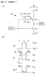
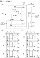
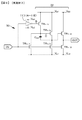
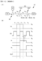
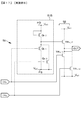
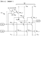
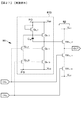
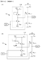
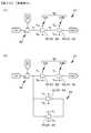
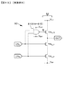
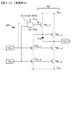
実施例1は、本発明のインバータ回路に関する。図1の(A)は、実施例1に係るインバータ回路10の回路図である。図1の(B)は、図1の(A)に示すインバータ回路10の動作を説明するための模式的なタイミングチャートである。
Example 1 relates to an inverter circuit of the present invention. FIG. 1A is a circuit diagram of an
実施例1のインバータ回路10は、同一導電型のトランジスタから成るインバータ回路であって、インバータ回路10は否定論理構成部11と出力回路部12とから構成されている。出力回路部12は同一導電型の2つのトランジスタから構成されている。出力回路部12を構成する2つのトランジスタを、第1出力トランジスタTRn_11、及び、第2出力トランジスタTRn_12と表すとき、第1出力トランジスタTRn_11の一方のソース/ドレイン領域と第2出力トランジスタTRn_12の一方のソース/ドレイン領域とは接続されている。第2出力トランジスタTRn_12のゲート電極は、否定論理構成部11の出力側に接続されている。第1出力トランジスタTRn_11の他方のソース/ドレイン領域には第1電圧Vss1(例えば0ボルト)が印加され、第2出力トランジスタTRn_12の他方のソース/ドレイン領域には第2電圧Vdd1(例えば10ボルト)が印加され、第1出力トランジスタTRn_11のゲート電極、及び、否定論理構成部11の入力側には、入力信号INが印加される。第2出力トランジスタTRn_12のゲート電極と否定論理構成部11の出力側の接続部を符号Bで示す。
The
インバータ回路10を構成する第1出力トランジスタTRn_11、及び、第2出力トランジスタTRn_12は、ソース/ドレイン領域、チャネル形成領域、及び、ゲート電極を備えた、nチャネル型の薄膜トランジスタ(TFT)から成る。これらのトランジスタは、図示せぬ基板上に形成されている。否定論理構成部11を構成するトランジスタにおいても同様である。
The first output transistor TR n — 11 and the second output transistor TR n — 12 constituting the
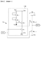
否定論理構成部11は種々の構成をとり得る。実施例1においては、5種の構成(符号11A乃至11Eを付して表す否定論理構成部)について説明するが、先ず、共通する動作について説明する。
The negative
実施例1のインバータ回路10にあっては、第1出力トランジスタTRn_11をオフ状態とする入力信号INが印加されたとき、第2出力トランジスタTRn_12のゲート電極には、否定論理構成部11の出力側から第2出力トランジスタTRn_12のオン状態を維持するのに足りる電圧が印加される。第1出力トランジスタTRn_11をオン状態とする入力信号INが印加されたとき、第2出力トランジスタTRn_12のゲート電極には、否定論理構成部11の出力側から第2出力トランジスタTRn_12のオフ状態を維持するのに足りる電圧が印加される。出力信号OUTは、第1出力トランジスタTRn_11の一方のソース/ドレイン領域と第2出力トランジスタTRn_12の一方のソース/ドレイン領域との接続部から出力される。
In the
図1の(B)を参照して、図1の(A)に示すインバータ回路10の動作を説明する。図1の(B)は、入力信号INの電圧、接続部Bの電圧、出力信号OUTの電圧を模式的に示したタイミングチャートである。図1の(B)に示す期間T1,T3においては、第1出力トランジスタTRn_11はオフ状態となる。一方、第2出力トランジスタTRn_12の閾値電圧をVth_12と表すとき、期間T1,T3において、第2出力トランジスタTRn_12のゲート電極には、否定論理構成部11の出力側から(Vdd1+Vth_12)を越える電圧VB1,VB3が印加される。期間T2において、第2出力トランジスタTRn_12のゲート電極には、否定論理構成部11の出力側から(Vss1+Vth_12)を越えない電圧VB2が印加される。
The operation of the
従って、第1出力トランジスタTRn_11をオフ状態とする入力信号INが印加されたとき、出力電圧として第2電圧Vdd1が出力される。一方、第1出力トランジスタTRn_11をオン状態とする入力信号INが印加されたときには出力電圧として第1電圧Vss1が出力される。 Therefore, when the input signal IN that turns off the first output transistor TR n — 11 is applied, the second voltage V dd1 is output as the output voltage. On the other hand, when the input signal IN for turning on the first output transistor TR n — 11 is applied, the first voltage V ss1 is output as the output voltage.
この構成においては、否定論理構成部11は専ら第2出力トランジスタTRn_12のゲート電極の電圧を制御するために用いられるに過ぎない。従って、消費電力を低減する観点からは、否定論理構成部11を構成するトランジスタは、第1出力トランジスタTRn_11や第2出力トランジスタTRn_12に対し相対的に小さいサイズとして設計することが好ましい。このように設計された実施例1のインバータ回路10によれば、否定論理構成部11に貫通電流が流れるとしても、インバータ回路全体としての消費電力を抑えることができる。
In this configuration, the negative
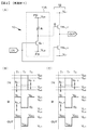
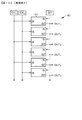
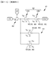
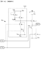
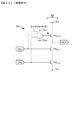
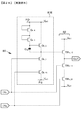
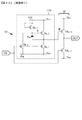
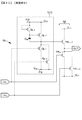
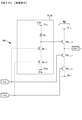
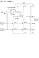
次いで、図2の(A)乃至(C)を参照して、否定論理構成部11Aを備えたインバータ回路10の構成と動作について説明する。図2の(A)は、実施例1に係るインバータ回路10の回路図である。図2の(B)及び(C)は、図2の(A)に示すインバータ回路10の動作を説明するための模式的なタイミングチャートである。
Next, the configuration and operation of the
否定論理構成部11Aは、同一導電型(nチャネル型)のトランジスタQn_1、及び、抵抗R1から構成されている。トランジスタQn_1のゲート電極は、否定論理構成部11Aの入力側を構成する。トランジスタQn_1の一方のソース/ドレイン領域は、抵抗R1の一端に接続されており、否定論理構成部11Aの出力側を構成する。抵抗R1の他端は一方の電圧供給線PDに接続されている。トランジスタQn_1の他方のソース/ドレイン領域は他方の電圧供給線PSに接続されている。
The negative
否定論理構成部11Aは、基本的には、背景技術において図53の(A)を参照して説明した周知のインバータ回路と同様の構成である。
The negative
一方の電圧供給線PDには電圧Vdd0が印加され、他方の電圧供給線PSには電圧Vss0が印加される。第2出力トランジスタTRn_12の閾値電圧をVth_12と表すとき(以下の他の実施例においても同様である)、電圧Vdd0は、Vdd0>(Vdd1+Vth_12)を満たすように定められた所定の電圧である。即ち、基本的には、Vdd1<Vdd0という関係を満たす電圧である。電圧Vss0は、トランジスタQn_1のオン抵抗と抵抗R1の分圧により定まる電圧が(Vss1+Vth_12)を越えないように定められた所定の電圧である。基本的にはVss0≦Vss1の関係を満たす電圧である。 The one voltage supply line PD is applied a voltage V dd0, the other voltage supply line PS is the voltage V ss0 applied. When the threshold voltage of the second output transistor TR n — 12 is expressed as V th — 12 (the same applies to the other embodiments below), the voltage V dd0 is determined to satisfy V dd0 > (V dd1 + V th — 12 ). It is a predetermined voltage. That is, the voltage basically satisfies the relationship V dd1 <V dd0 . The voltage V ss0 is a predetermined voltage determined so that the voltage determined by the on-resistance of the transistor Q n_1 and the divided voltage of the resistor R 1 does not exceed (V ss1 + V th — 12 ). Basically, the voltage satisfies the relationship of V ss0 ≦ V ss1 .
図2の(B)を参照して、図2の(A)に示すインバータ回路10の動作を説明する。図2の(B)に示す期間T1,T3においては、第1出力トランジスタTRn_11はオフ状態となる。一方、期間T1,T3において、第2出力トランジスタTRn_12のゲート電極には、否定論理構成部11Aの出力側から(Vdd1+Vth_12)を越える電圧Vdd0が印加される。期間T2において、第2出力トランジスタTRn_12のゲート電極には、否定論理構成部11の出力側から(Vss1+Vth_12)を越えない電圧VB2が印加される。
The operation of the
従って、第1出力トランジスタTRn_11をオフ状態とする入力信号INが印加されたとき、出力電圧として第2電圧Vdd1が出力される。一方、第1出力トランジスタTRn_11をオン状態とする入力信号INが印加されたときには出力電圧として第1電圧Vss1が出力される。 Therefore, when the input signal IN that turns off the first output transistor TR n — 11 is applied, the second voltage V dd1 is output as the output voltage. On the other hand, when the input signal IN for turning on the first output transistor TR n — 11 is applied, the first voltage V ss1 is output as the output voltage.
尚、背景技術で説明したと同様に、否定論理構成部11Aにあっては、入力信号INはトランジスタQn_1のゲート−ソース間電圧(Vgs)となる。入力信号INのハイレベルが電圧Vdd0に至らない場合であっても、インバータ回路10は動作する。具体的には、図2の(C)に示すように、期間T2において入力信号INの値がトランジスタQn_1の閾値電圧Vth_1を超えれば、インバータ回路10の出力はハイレベルからローレベルへと向かう。従って、インバータ回路10はレベルシフタとしても動作する。
As described in the background art, in the negative
また、入力信号INのローレベルが電圧Vss0に至らない場合であっても、インバータ回路10は動作する。具体的には、図2の(C)に示すように、期間T1,T3において入力信号INがトランジスタQn_1の閾値電圧Vth_1と第1出力トランジスタTRn_11の閾値電圧Vth_11を越えなければ、動作上支障を生ずることはない。
Even if the low level of the input signal IN does not reach the voltage V ss0 , the
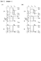
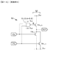
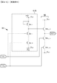
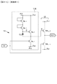
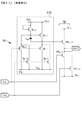
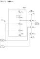
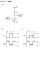
次いで、図3を参照して、否定論理構成部11Bを備えたインバータ回路10の構成を説明する。図3は、実施例1に係るインバータ回路10の回路図である。
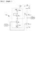
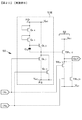
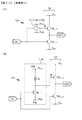
Next, the configuration of the
否定論理構成部11Bは、同一導電型の第1トランジスタQn_1、及び、第2トランジスタQn_2から構成されている。第1トランジスタQn_1のゲート電極は、否定論理構成部11Bの入力側を構成する。第1トランジスタQn_1の一方のソース/ドレイン領域は、第2トランジスタQn_2の一方のソース/ドレイン領域に接続されており、否定論理構成部11Bの出力側を構成する。第2トランジスタQn_2の他方のソース/ドレイン領域は一方の電圧供給線PDに接続されている。第2トランジスタQn_2のゲート電極は、第2トランジスタQn_2の他方のソース/ドレイン領域に接続されている。第1トランジスタQn_1の他方のソース/ドレイン領域は、他方の電圧供給線PSに接続されている。
The negative
否定論理構成部11Bは、基本的には、背景技術において図54の(A)を参照して説明した周知のインバータ回路と同様の構成である。否定論理構成部11Bは、図2の(A)に示す抵抗R1を所謂ダイオード接続されたnチャネル型のトランジスタQn_2で置き換えた構成である。
The negation
図53の(A)を参照して説明したと同様に、一方の電圧供給線PDには電圧Vdd0が印加され、他方の電圧供給線PSには電圧Vss0が印加される。第2トランジスタQn_2の閾値電圧をVth_2と表すとき(以下の他の実施例においても同様である)、電圧Vdd0は、(Vdd0−Vth_2)>(Vdd1+Vth_12)を満たすように定められた所定の電圧である。即ち、基本的には、Vdd1<Vdd0という関係を満たす電圧である。電圧Vss0は、トランジスタQn_1のオン抵抗とトランジスタQn_2の抵抗値の分圧により定まる電圧が(Vss1+Vth_12)を越えないように定められた所定の電圧である。トランジスタQn_1のオン抵抗にもよるが、基本的にはVss0≦Vss1の関係を満たす電圧である。否定論理構成部11Bを備えたインバータ回路10の動作は、基本的には図2の(B)及び(C)を参照して説明したと同様であるので、説明を省略する。
In the same manner as described with reference to FIG. 53 (A), the one voltage supply line PD is applied a voltage V dd0, the other voltage supply line PS is the voltage V ss0 applied. When the threshold voltage of the second transistor Q n_2 is represented as V th_2 (the same applies to the other embodiments below), the voltage V dd0 satisfies (V dd0 −V th_2 )> (V dd1 + V th — 12 ). Is a predetermined voltage. That is, the voltage basically satisfies the relationship V dd1 <V dd0 . The voltage V ss0 is a predetermined voltage determined so that the voltage determined by the divided voltage of the on-resistance of the transistor Q n_1 and the resistance value of the transistor Q n_2 does not exceed (V ss1 + V th — 12 ). Although depending on the on-resistance of the transistor Q n_1, the voltage basically satisfies the relationship of V ss0 ≦ V ss1 . Since the operation of the
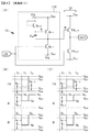
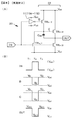
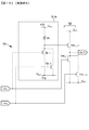
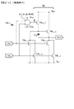
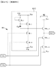
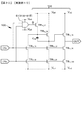
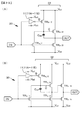
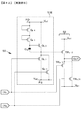
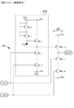
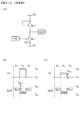
次いで、図4を参照して、否定論理構成部11Cを備えたインバータ回路10の構成を説明する。図4の(A)は、実施例1に係るインバータ回路10の回路図である。図4の(B)及び(C)は、図4の(A)に示すインバータ回路10の動作を説明するための模式的なタイミングチャートである。
Next, the configuration of the
否定論理構成部11は、同一導電型の第1トランジスタQn_1、第2トランジスタQn_2、及び、第3トランジスタQn_3から構成されており、
第1トランジスタQn_1においては、
(A−1)ゲート電極は、否定論理構成部11Cの入力側を構成し、
(A−2)一方のソース/ドレイン領域は、第2トランジスタQn_2の一方のソース/ドレイン領域に接続されており、否定論理構成部11Cの出力側を構成し、
第2トランジスタQn_2においては、
(B−1)他方のソース/ドレイン領域は一方の電圧供給線PDに接続されており、
(B−2)ゲート電極は、第3トランジスタQn_3の一方のソース/ドレイン領域に接続されており、
第3トランジスタQn_3においては、
(C−1)ゲート電極は他方のソース/ドレイン領域に接続されており、
(C−2)他方のソース/ドレイン領域は一方の電圧供給線PDに接続されており、
第1トランジスタQn_1の他方のソース/ドレイン領域は、他方の電圧供給線PSに接続されている。
The negative
In the first transistor Q n_1 ,
(A-1) The gate electrode constitutes the input side of the
(A-2) One source / drain region is connected to one source / drain region of the second transistor Q n_2 and constitutes the output side of the negative
In the second transistor Q n_2 ,
(B-1) The other source / drain region is connected to one voltage supply line PD,
(B-2) The gate electrode is connected to one source / drain region of the
In the third transistor Q n_3 ,
(C-1) The gate electrode is connected to the other source / drain region,
(C-2) The other source / drain region is connected to one voltage supply line PD,
The other source / drain region of the first transistor Q n_1 is connected to the other voltage supply line PS.
否定論理構成部11Cは、基本的には、背景技術において図55の(A)を参照して説明した、所謂ブートストラップ動作を利用した周知のインバータ回路と同様の構成である。第2トランジスタQn_2のゲート電極は第3トランジスタQn_3の一方のソース/ドレイン領域に接続されており、ノードAを構成する。第3トランジスタQn_3がオン状態からオフ状態になると、ノードAは浮遊状態となる。第2トランジスタQn_2のゲート電極と一方のソース/ドレイン領域との間にブートストラップ容量としての容量部Capが接続されている。
The negative
図55の(A)を参照して説明したと同様に、一方の電圧供給線PDには電圧Vdd0が印加され、他方の電圧供給線PSには電圧Vss0が印加される。電圧Vdd0は、Vdd0>(Vdd1+Vth_12)を満たすように定められた所定の電圧である。即ち、基本的には、Vdd1<Vdd0という関係を満たす電圧である。電圧Vss0は、トランジスタQn_1のオン抵抗とトランジスタQn_2の抵抗値の分圧により定まる電圧が(Vss1+Vth_12)を越えないように定められた所定の電圧である。基本的にはVss0≦Vss1の関係を満たす電圧である。 In the same manner as described with reference to FIG. 55 (A), the one voltage supply line PD is applied a voltage V dd0, the other voltage supply line PS is the voltage V ss0 applied. The voltage V dd0 is a predetermined voltage determined so as to satisfy V dd0 > (V dd1 + V th — 12 ). That is, the voltage basically satisfies the relationship V dd1 <V dd0 . The voltage V ss0 is a predetermined voltage determined so that the voltage determined by the divided voltage of the on-resistance of the transistor Q n_1 and the resistance value of the transistor Q n_2 does not exceed (V ss1 + V th — 12 ). Basically, the voltage satisfies the relationship of V ss0 ≦ V ss1 .
図4の(B)を参照して、図4の(A)に示すインバータ回路10の動作を説明する。図4の(B)は、入力信号INの電圧、ノードAの電圧、接続部Bの電圧を模式的に示したタイミングチャートである。図4の(B)の期間T1,T3においてノードAの電圧(電位)VA1,VA3がブートストラップ動作により(Vdd0+Vth_2)を越えるように、否定論理構成部11Cの構成、及び、電圧Vss0,Vdd0の値は設定されている。
The operation of the
更には、否定論理構成部11Cの構成、及び、電圧Vss0,Vdd0の値は、以下の条件を満たすように設定されている。即ち、第3トランジスタQn_3の閾値電圧をVth_3と表すとき(以下の他の実施例においても同様である)、期間T2にあっては、ノードAの電位VA2は(Vdd0−Vth_3)となる。期間T2における接続部Bの電圧VB2は、トランジスタQn_1のオン抵抗の値とトランジスタQn_2の抵抗値との分圧比によって定まる。電圧VB2が(Vss1+Vth_12)を越えないように、否定論理構成部11Cの構成、及び、電圧Vss0,Vdd0の値は設定されている。
Furthermore, the configuration of the negative
従って、第1出力トランジスタTRn_11をオフ状態とする入力信号INが印加されたとき、出力電圧として第2電圧Vdd1が出力される。一方、第1出力トランジスタTRn_11をオン状態とする入力信号INが印加されたときには出力電圧として第1電圧Vss1が出力される。 Therefore, when the input signal IN that turns off the first output transistor TR n — 11 is applied, the second voltage V dd1 is output as the output voltage. On the other hand, when the input signal IN for turning on the first output transistor TR n — 11 is applied, the first voltage V ss1 is output as the output voltage.
尚、背景技術で説明したと同様に、否定論理構成部11Cにおいても、入力信号INはトランジスタQn_1のゲート−ソース間電圧(Vgs)となる。入力信号INのハイレベルが電圧Vdd0に至らない場合であっても、インバータ回路10は動作する。具体的には、図2の(C)に示すように、期間T2において入力信号INの値がトランジスタQn_1の閾値電圧Vth_1を超えれば、インバータ回路10の出力はハイレベルからローレベルへと向かう。従って、インバータ回路10はレベルシフタとしても動作する。
As described in the background art, also in the negative
また、入力信号INのローレベルが電圧Vss0に至らない場合であっても、インバータ回路10は動作する。具体的には、図4の(C)に示すように、期間T1,T3において入力信号INがトランジスタQn_1の閾値電圧Vth_1と第1出力トランジスタTRn_11の閾値電圧Vth_11を越えなければ、動作上支障を生ずることはない。
Even if the low level of the input signal IN does not reach the voltage V ss0 , the
次いで、図5を参照して、否定論理構成部11Dを備えたインバータ回路10の構成を説明する。図5の(A)は、実施例1に係るインバータ回路10の回路図である。図5の(B)及び(C)は、図5の(A)に示すインバータ回路10の動作を説明するための模式的なタイミングチャートである。
Next, the configuration of the
否定論理構成部11Dは、同一導電型の第1トランジスタQn_1、第2トランジスタQn_2、及び、第3トランジスタQn_3から構成されており、
第1トランジスタQn_1においては、
(A−1)ゲート電極は、否定論理構成部11の入力側を構成し、
(A−2)一方のソース/ドレイン領域は、第2トランジスタQn_2の一方のソース/ドレイン領域に接続されており、否定論理構成部11の出力側を構成し、
第2トランジスタQn_2においては、
(B−1)他方のソース/ドレイン領域は一方の電圧供給線PDに接続されており、
(B−2)ゲート電極は、第3トランジスタQn_3の一方のソース/ドレイン領域に接続されており、
第3トランジスタQn_3においては、
(C−1)ゲート電極は他方のソース/ドレイン領域に接続されており、
否定論理構成部11は、更に、同一導電型の第4トランジスタQn_4を備えており、
第3トランジスタQn_3の他方のソース/ドレイン領域は一方の電圧供給線PDに接続されており、
第4トランジスタQn_4の一方のソース/ドレイン領域は、第2トランジスタQn_2のゲート電極と第3トランジスタQn_3の一方のソース/ドレイン領域とに接続されており、
第1トランジスタQn_1の他方のソース/ドレイン領域及び第4トランジスタQn_4の他方のソース/ドレイン領域は、他方の電圧供給線PSに接続されており、
第4トランジスタQn_4のゲート電極には入力信号INが印加される。
The negative
In the first transistor Q n_1 ,
(A-1) The gate electrode constitutes the input side of the negative
(A-2) One source / drain region is connected to one source / drain region of the second transistor Q n_2 , and constitutes the output side of the negative
In the second transistor Q n_2 ,
(B-1) The other source / drain region is connected to one voltage supply line PD,
(B-2) The gate electrode is connected to one source / drain region of the
In the third transistor Q n_3 ,
(C-1) The gate electrode is connected to the other source / drain region,
The negative
The other source / drain region of the
One source / drain region of the fourth transistor Q n_4 is connected to the gate electrode of the second transistor Q n_2 and one source / drain region of the third transistor Q n_3 ,
The other source / drain region of the first transistor Q n_1 and the other source / drain region of the fourth transistor Q n_4 are connected to the other voltage supply line PS,
The input signal IN is applied to the gate electrode of the
否定論理構成部11Dは、図4の(A)に示すブートストラップ動作を利用した否定論理構成部11Cに対し、ノードAに接続された第4トランジスタQn_4が追加された構成である。図5の(B)に示すタイミングチャートは、図4の(B)に示すタイミングチャートと対応する。また、図5の(C)に示すタイミングチャートは、図4の(C)に示すタイミングチャートと対応する。
The negative
図4の(A)を参照して説明したと同様に、一方の電圧供給線PDには電圧Vdd0が印加され、他方の電圧供給線PSには電圧Vss0が印加される。電圧Vdd0は、Vdd0>(Vdd1+Vth_12)を満たすように定められた所定の電圧である。即ち、基本的には、Vdd1<Vdd0という関係を満たす電圧である。電圧Vss0は、トランジスタQn_1のオン抵抗とトランジスタQn_2の抵抗値の分圧により定まる電圧が(Vss1+Vth_12)を越えないように定められた所定の電圧である。基本的にはVss0≦Vss1の関係を満たす電圧である。 In the same manner as described with reference to FIG. 4 (A), the one voltage supply line PD is applied a voltage V dd0, the other voltage supply line PS is the voltage V ss0 applied. The voltage V dd0 is a predetermined voltage determined so as to satisfy V dd0 > (V dd1 + V th — 12 ). That is, the voltage basically satisfies the relationship V dd1 <V dd0 . The voltage V ss0 is a predetermined voltage determined so that the voltage determined by the divided voltage of the on-resistance of the transistor Q n_1 and the resistance value of the transistor Q n_2 does not exceed (V ss1 + V th — 12 ). Basically, the voltage satisfies the relationship of V ss0 ≦ V ss1 .
図4の(A)に示す否定論理構成部11Cにあっては、期間T2においてノードAの電位VA2は(Vdd0−Vth_3)であり、接続部Bの電圧VB2の値はトランジスタQn_1のオン抵抗の値と、ゲート電極に(Vdd0−Vth_3)が印加された状態のトランジスタQn_2の抵抗値との分圧比によって定まる。これに対し、図5の(A)に示す否定論理構成部11Dにあっては、第1トランジスタQn_1をオン状態とする入力信号INが印加された状態において、第4トランジスタQn_4もオン状態となる。従って、図5の(B)に示すように、期間T2において、上記ノードAの電位VA2は、(Vdd0−Vth_3)から他方の電圧供給線PSの電位Vss0側に近づく。
In the negative
電圧VB2の値は第1トランジスタQn_1のオン抵抗の値と、ゲート電極により低い値の電圧が印加された状態の第2トランジスタQn_2の抵抗値との分圧比によって定まる。従って、期間T2における接続部Bの電圧VB2の値をよりVss0に近づけることができる。これにより、否定論理構成部11Dの貫通電流をより小さくすることができるし、図4の(A)に示す構成よりも、電圧Vss0と電圧Vss1の差を小さく設定することができるといった利点を有する。
The value of the voltage V B2 is determined by the voltage division ratio between the on-resistance value of the first transistor Q n_1 and the resistance value of the second transistor Q n_2 in a state where a low value voltage is applied by the gate electrode. Accordingly, the value of the voltage V B2 at the connection portion B in the period T 2 can be made closer to V ss0 . Thereby, the through current of the negative
上述した点が相違する他、インバータ回路10の動作は図4の(A)乃至(C)を参照して説明したと同様である。否定論理構成部11Dにおいても、入力信号INはトランジスタQn_1のゲート−ソース間電圧(Vgs)となる。入力信号INのハイレベルが電圧Vdd0に至らない場合であっても、インバータ回路10は動作する。具体的には、図5の(C)に示すように、期間T2において入力信号INの値がトランジスタQn_1の閾値電圧Vth_1を超えれば、インバータ回路10の出力はハイレベルからローレベルへと向かう。従って、インバータ回路10はレベルシフタとしても動作する。
In addition to the differences described above, the operation of the
また、入力信号INのローレベルが電圧Vss0に至らない場合であっても、インバータ回路10は動作する。具体的には、図5の(C)に示すように、期間T1,T3において入力信号INがトランジスタQn_1の閾値電圧Vth_1、トランジスタQn_4の閾値電圧Vth_4(図示せず)、及び、第1出力トランジスタTRn_11の閾値電圧Vth_11を越えなければ、動作上支障を生ずることはない。
Even if the low level of the input signal IN does not reach the voltage V ss0 , the
次いで、図6、図7の(A)及び(B)を参照して、否定論理構成部11Eを備えたインバータ回路10の構成を説明する。図6は、実施例1に係るインバータ回路10の回路図である。図7の(A)及び(B)は、図6に示すインバータ回路10の動作を説明するための模式的なタイミングチャートである。
Next, the configuration of the
否定論理構成部11Eは、同一導電型の第1トランジスタQn_1、第2トランジスタQn_2、及び、第3トランジスタQn_3から構成されており、
第1トランジスタQn_1においては、
(A−1)ゲート電極は、否定論理構成部11Eの入力側を構成し、
(A−2)一方のソース/ドレイン領域は、第2トランジスタQn_2の一方のソース/ドレイン領域に接続されており、否定論理構成部11Eの出力側を構成し、
第2トランジスタQn_2においては、
(B−1)他方のソース/ドレイン領域は一方の電圧供給線PDに接続されており、
(B−2)ゲート電極は、第3トランジスタQn_3の一方のソース/ドレイン領域に接続されており、
第3トランジスタQn_3においては、
(C−1)ゲート電極は他方のソース/ドレイン領域に接続されており、
否定論理構成部11Eは、更に、同一導電型の第4トランジスタQn_4を備えており、
第3トランジスタQn_3の他方のソース/ドレイン領域は第4トランジスタQn_4の一方のソース/ドレイン領域に接続されており、
第4トランジスタQn_4のゲート電極は第4トランジスタQn_4の他方のソース/ドレイン領域に接続されており、
第4トランジスタQn_4の他方のソース/ドレイン領域は一方の電圧供給線PDに接続されており、
第1トランジスタQn_1の他方のソース/ドレイン領域は他方の電圧供給線PSに接続されている。
The negative
In the first transistor Q n_1 ,
(A-1) The gate electrode constitutes the input side of the
(A-2) One source / drain region is connected to one source / drain region of the second transistor Q n_2 and constitutes the output side of the negative
In the second transistor Q n_2 ,
(B-1) The other source / drain region is connected to one voltage supply line PD,
(B-2) The gate electrode is connected to one source / drain region of the
In the third transistor Q n_3 ,
(C-1) The gate electrode is connected to the other source / drain region,
The negative
The other source / drain region of the third transistor Q n_3 is connected to one source / drain region of the fourth transistor Q n_4 ,
The gate electrode of the fourth transistor Q n_4 is connected to the other source / drain region of the fourth transistor Q n_4,
The other source / drain region of the
The other source / drain region of the first transistor Q n_1 is connected to the other voltage supply line PS.
否定論理構成部11Eは、図4の(A)に示すブートストラップ動作を利用した否定論理構成部11Cに対し、第3トランジスタQn_3に第4トランジスタQn_4が直列に接続された構成である。図7の(A)に示すタイミングチャートは、図4の(B)に示すタイミングチャートと対応する。また、図7の(B)に示すタイミングチャートは、図4の(C)に示すタイミングチャートと対応する。
The negative
図4の(A)を参照して説明したと同様に、一方の電圧供給線PDには電圧Vdd0が印加され、他方の電圧供給線PSには電圧Vss0が印加される。電圧Vdd0は、Vdd0>(Vdd1+Vth_12)を満たすように定められた所定の電圧である。即ち、基本的には、Vdd1<Vdd0という関係を満たす電圧である。電圧Vss0は、トランジスタQn_1のオン抵抗とトランジスタQn_2の抵抗値の分圧により定まる電圧が(Vss1+Vth_12)を越えないように定められた所定の電圧である。基本的にはVss0≦Vss1の関係を満たす電圧である。 In the same manner as described with reference to FIG. 4 (A), the one voltage supply line PD is applied a voltage V dd0, the other voltage supply line PS is the voltage V ss0 applied. The voltage V dd0 is a predetermined voltage determined so as to satisfy V dd0 > (V dd1 + V th — 12 ). That is, the voltage basically satisfies the relationship V dd1 <V dd0 . The voltage V ss0 is a predetermined voltage determined so that the voltage determined by the divided voltage of the on-resistance of the transistor Q n_1 and the resistance value of the transistor Q n_2 does not exceed (V ss1 + V th — 12 ). Basically, the voltage satisfies the relationship of V ss0 ≦ V ss1 .
図4の(A)に示す否定論理構成部11Cにあっては、期間T2においてノードAの電位VA2は(Vdd0−Vth_3)であり、接続部Bの電圧VB2の値はトランジスタQn_1のオン抵抗の値と、ゲート電極に(Vdd0−Vth_3)が印加された状態のトランジスタQn_2の抵抗値との分圧比によって定まる。これに対し、図6に示す否定論理構成部11Eにあっては、ダイオード接続された第4トランジスタQn_4が、第3トランジスタQn_3に直列に接続された構成となる。従って、第4トランジスタQn_4の閾値電圧をVth_4と表せば、ハイレベルの入力信号INが印加された状態にあっては、上記ノードAの電位は(Vdd0−Vth_3−Vth_4)となり、第4トランジスタQn_4の閾値電圧Vth_4分だけ他方の電圧供給線PSの電位Vss0側に近づく。
In the negative
電圧VB2の値は第1トランジスタQn_1のオン抵抗の値と、ゲート電極により低い値の電圧が印加された状態の第2トランジスタQn_2の抵抗値との分圧比によって定まる。従って、期間T2における接続部Bの電圧VB2の値をよりVss0に近づけることができる。これにより、否定論理構成部11Eの貫通電流をより小さくすることができるし、図4の(A)に示す構成よりも、電圧Vss0と電圧Vss1の差を小さく設定することができるといった利点を有する。
The value of the voltage V B2 is determined by the voltage division ratio between the on-resistance value of the first transistor Q n_1 and the resistance value of the second transistor Q n_2 in a state where a low value voltage is applied by the gate electrode. Accordingly, the value of the voltage V B2 at the connection portion B in the period T 2 can be made closer to V ss0 . Thereby, the through current of the negative
上述した点が相違する他、インバータ回路10の動作は図4の(A)乃至(C)を参照して説明したと同様である。否定論理構成部11Eにおいても、入力信号INはトランジスタQn_1のゲート−ソース間電圧(Vgs)となる。入力信号INのハイレベルが電圧Vdd0に至らない場合であっても、インバータ回路10は動作する。具体的には、図7の(B)に示すように、期間T2において入力信号INの値がトランジスタQn_1の閾値電圧Vth_1を超えれば、インバータ回路10の出力はハイレベルからローレベルへと向かう。従って、インバータ回路10はレベルシフタとしても動作する。
In addition to the differences described above, the operation of the
また、入力信号INのローレベルが電圧Vss0に至らない場合であっても、インバータ回路10は動作する。具体的には、図7の(B)に示すように、期間T1,T3において入力信号INがトランジスタQn_1の閾値電圧Vth_1と第1出力トランジスタTRn_11の閾値電圧Vth_11を越えなければ、動作上支障を生ずることはない。
Even if the low level of the input signal IN does not reach the voltage V ss0 , the
図7の(A)の期間T2においてノードAの電位を低下させる方法として、設計的に第3トランジスタQn_3の閾値電圧を大きくするという手段もとり得るが、トランジスタの製造上必ずしも容易であるとはいえない。上述した構成によれば、単にダイオード接続されたトランジスタを追加するといった簡便な手段により、ノードAの電位を低下させることができる。尚、場合によっては、更にダイオード接続されたトランジスタを追加した構成とすることもできる。
As a method of reducing the potential of the node A in the period T 2 in FIG. 7A , a means of increasing the threshold voltage of the
実施例2も、本発明のインバータ回路に関する。図8の(A)は、実施例2に係るインバータ回路20の回路図である。図8の(B)は、図8の(A)に示すインバータ回路20の動作を説明するための模式的なタイミングチャートである。
Example 2 also relates to the inverter circuit of the present invention. FIG. 8A is a circuit diagram of the
実施例2のインバータ回路20も、同一導電型のトランジスタから成るインバータ回路であって、インバータ回路20は否定論理構成部11と出力回路部22とから構成されている。出力回路部22は同一導電型の2つのトランジスタから構成されている。出力回路部22を構成する2つのトランジスタを、第1出力トランジスタTRn_11、及び、第2出力トランジスタTRn_12と表すとき、第1出力トランジスタTRn_11の一方のソース/ドレイン領域と第2出力トランジスタTRn_12の一方のソース/ドレイン領域とは接続されている。第2出力トランジスタTRn_12のゲート電極は、否定論理構成部11の出力側に接続されている。第1出力トランジスタTRn_11の他方のソース/ドレイン領域には第1電圧Vss1が印加され、第2出力トランジスタTRn_12の他方のソース/ドレイン領域には第2電圧Vdd1が印加され、第1出力トランジスタTRn_11のゲート電極、及び、否定論理構成部11の入力側には、入力信号INが印加される。第2出力トランジスタTRn_12のゲート電極と否定論理構成部11の出力側の接続部を符号Bで示す。
The
実施例1において説明したと同様に、否定論理構成部11は種々の構成をとり得る。否定論理構成部11(符号11A乃至11E)の構成及び動作は、実施例1において説明したと同様であるので、説明を省略する。
As described in the first embodiment, the negative
実施例2のインバータ回路20にあっては、出力回路部22は、更に、同一導電型の2つのトランジスタを備えている。これら2つのトランジスタを、第3出力トランジスタTRn_23、及び、第4出力トランジスタTRn_24と表すとき、第3出力トランジスタTRn_23の一方のソース/ドレイン領域と第4出力トランジスタTRn_24の一方のソース/ドレイン領域とは接続されている。第4出力トランジスタTRn_24のゲート電極は、第1出力トランジスタTRn_11の一方のソース/ドレイン領域と第2出力トランジスタTRn_12の一方のソース/ドレイン領域とに接続されている。第3出力トランジスタTRn_23の他方のソース/ドレイン領域には第1電圧Vss1が印加され、第4出力トランジスタTRn_24の他方のソース/ドレイン領域には第2電圧Vdd1が印加される。第3出力トランジスタTRn_23のゲート電極には入力信号INが印加される。第1出力トランジスタTRn_11及び第3出力トランジスタTRn_23をオフ状態とする入力信号INが印加されたとき、第4出力トランジスタTRn_24のゲート電極には、ブートストラップ動作により第4出力トランジスタTRn_24のオン状態を維持するのに足りる電圧が印加される。第1出力トランジスタTRn_11及び第3出力トランジスタTRn_23をオン状態とする入力信号INが印加されたとき、第4出力トランジスタTRn_24のゲート電極には、第4出力トランジスタTRn_24のオフ状態を維持するのに足りる電圧が印加される。出力信号OUTは、第3出力トランジスタTRn_23の一方のソース/ドレイン領域と第4出力トランジスタTRn_24の一方のソース/ドレイン領域との接続部から出力される。
In the
尚、第4出力トランジスタTRn_24のゲート電極と一方のソース/ドレイン領域との間にブートストラップ容量としての容量部Cap2が接続されている。第4出力トランジスタTRn_24のゲート電極と、第1出力トランジスタTRn_11一方のソース/ドレイン領域及び第2出力トランジスタTRn_12一方のソース/ドレイン領域との接続部を符号Cで表す。 A capacitor part C ap2 as a bootstrap capacitor is connected between the gate electrode of the fourth output transistor TR n — 24 and one of the source / drain regions. A connection portion between the gate electrode of the fourth output transistor TR n — 24 and one source / drain region of the first output transistor TR n — 11 and one source / drain region of the second output transistor TR n — 12 is denoted by reference symbol C.
図8の(B)は、入力信号INの電圧、接続部Bの電圧、接続部Cの電圧、出力信号OUTの電圧を模式的に示したタイミングチャートである。第4出力トランジスタTRn_24の閾値電圧をVth_24と表す。図8の(B)の期間T1,T3において接続部Cの電圧(電位)VC1,VC3がブートストラップ動作により(Vdd1+Vth_24)を越えるように、出力回路部22は構成されている。
FIG. 8B is a timing chart schematically showing the voltage of the input signal IN, the voltage of the connection portion B, the voltage of the connection portion C, and the voltage of the output signal OUT. The threshold voltage of the fourth output transistor TR n — 24 is represented as V th — 24 . The
従って、図8の(B)の期間T1,T3においては、出力電圧VOUT1,VOUT3として第2電圧Vdd1が出力される。一方、図8の(B)の期間T2において、第1出力トランジスタTRn_11及び第3出力トランジスタTRn_23をオン状態とする入力信号INが印加されたときには出力電圧VOUT2として第1電圧Vss1が出力される。これにより、第1電圧Vss1と第2電圧Vdd1とを出力電圧とする出力信号OUTを出力することができる。 Therefore, in the periods T 1 and T 3 in FIG. 8B , the second voltage V dd1 is output as the output voltages V OUT1 and V OUT3 . On the other hand, when the input signal IN for turning on the first output transistor TR n — 11 and the third output transistor TR n — 23 is applied in the period T 2 of FIG. 8B, the first voltage V ss1 is used as the output voltage V OUT2 . Is output. As a result, an output signal OUT having the first voltage V ss1 and the second voltage V dd1 as output voltages can be output.
実施例2のインバータ回路20にあっては、否定論理構成部11の出力側から第2出力トランジスタTRn_12のオン状態を維持するのに足りる電圧を印加する必要がない。従って、否定論理構成部11を動作させる電圧(より具体的には、電圧Vss0,Vdd0)の設定条件が緩和され、電源電圧の共通化に適するといった利点を有する。
In the
実施例3も、本発明のインバータ回路に関する。図9は、実施例3に係るインバータ回路30の回路図である。
Example 3 also relates to the inverter circuit of the present invention. FIG. 9 is a circuit diagram of the
実施例3のインバータ回路30も、同一導電型のトランジスタから成るインバータ回路であって、インバータ回路30は否定論理構成部11と出力回路部32とから構成されている。出力回路部32は、図8の(A)を参照して説明した出力回路部22に、更に、同一導電型の2つのトランジスタを加えた構成である。
The
即ち、出力回路部32は、更に、同一導電型の2つのトランジスタを備えており、これら2つのトランジスタを、第5出力トランジスタTRn_35、及び、第6出力トランジスタTRn_36と表すとき、第5出力トランジスタTRn_35の一方のソース/ドレイン領域と第6出力トランジスタの一方のソース/ドレイン領域とは接続されている。第6出力トランジスタTRn_36のゲート電極は、第3出力トランジスタTRn_23の一方のソース/ドレイン領域と第4出力トランジスタTRn_24の一方のソース/ドレイン領域とに接続されている。第5出力トランジスタTRn_35の他方のソース/ドレイン領域には第3電圧Vss2が印加される。第6出力トランジスタTRn_36の他方のソース/ドレイン領域には第4電圧Vdd2が印加される。第5出力トランジスタTRn_35のゲート電極には入力信号INが印加される。第1出力トランジスタTRn_11、第3出力トランジスタTRn_23、及び、第5出力トランジスタTRn_35をオフ状態とする入力信号INが印加されたとき、第6出力トランジスタTRn_36のゲート電極には、第3出力トランジスタTRn_23の一方のソース/ドレイン領域と第4出力トランジスタTRn_24の一方のソース/ドレイン領域との接続部から第6出力トランジスタTRn_36のオン状態を維持するのに足りる電圧が印加される。第1出力トランジスタTRn_11、第3出力トランジスタTRn_23、及び、第5出力トランジスタTRn_35をオン状態とする入力信号INが印加されたとき、第6出力トランジスタTRn_36のゲート電極には、第3出力トランジスタTRn_23の一方のソース/ドレイン領域と第4出力トランジスタTRn_24の一方のソース/ドレイン領域との接続部から第6出力トランジスタTRn_36のオフ状態を維持するのに足りる電圧が印加される。出力信号OUTは、第5出力トランジスタTRn_35の一方のソース/ドレイン領域と第6出力トランジスタTRn_36の一方のソース/ドレイン領域との接続部から出力される。
In other words, the
実施例1において説明したと同様に、否定論理構成部11は種々の構成をとり得る。否定論理構成部11(符号11A乃至11E)の構成及び動作は、実施例1において説明したと同様であるので、説明を省略する。
As described in the first embodiment, the negative
インバータ回路30において、第5出力トランジスタTRn_35と第6出力トランジスタTRn_36を除いた部分の構成及び動作は、図8の(A)を参照して説明したインバータ回路20の構成及び動作と同様であるので、説明省略する。第6出力トランジスタTRn_36の閾値電圧をVth_36と表すとき、電圧Vdd2は、Vdd1>(Vdd2+Vth_36)を満たすように定められた所定の電圧である。即ち、基本的には、Vdd2<Vdd1という関係を満たす電圧である。電圧Vss2は、基本的にはVss0≦Vss1≦Vss2の関係を満たす電圧である。
The configuration and operation of the
上述した構成のインバータ回路30にあっては、第1出力トランジスタTRn_11、第3出力トランジスタTRn_23、及び、第5出力トランジスタTRn_35をオン状態とする入力信号INが印加されたとき、第6出力トランジスタTRn_36のゲート電極には、第3出力トランジスタTRn_23の一方のソース/ドレイン領域と第4出力トランジスタTRn_24の一方のソース/ドレイン領域との接続部から第6出力トランジスタTRn_36のオフ状態を維持するのに足りる電圧が印加され、出力電圧として第3電圧Vss2が出力される。一方、第1出力トランジスタTRn_11、第3出力トランジスタTRn_23、及び、第5出力トランジスタTRn_35をオフ状態とする入力信号INが印加されたときには出力電圧として第4電圧Vdd2が出力される。第3電圧Vss2と第4電圧Vdd2との幅を、第1電圧Vss1と第2電圧Vdd1との幅よりも小さく設定することにより、インバータ回路の動作における信頼性の向上を図ることができる。換言すれば、トランジスタの特性ばらつきによる誤動作が発生し難いインバータ回路を構成することができる。
In the
実施例4は、本発明のシフトレジスタ回路に関する。図10は、実施例4に係るシフトレジスタ回路40の模式的な回路図である。図11は、図10に示すシフトレジスタ回路40の模式的なタイミングチャートである。
Example 4 relates to the shift register circuit of the present invention. FIG. 10 is a schematic circuit diagram of the
以下、シフトレジスタ回路40の各段目を構成するシフトレジスタ回路41の構成及び動作について説明する。先ず、発明の理解を助けるため、トランスファゲート部とバッファ回路を用いた回路の基本的な動作を説明する。図12の(A)は、トランスファゲート部とバッファ回路とから構成された回路の模式的な回路図を示す。図12の(B)は、図12の(A)に示す回路の動作を説明するための模式的なタイミングチャートである。尚、図12の(A)のトランスファゲート部とバッファ回路とは、それぞれ理想的な動作をするものとして説明する。
Hereinafter, the configuration and operation of the
図12の(B)に示す入力信号INをトランスファゲート部の一端に印加し、トランスファゲート部の他端をバッファ回路の入力側に接続する。そして、トランスファゲート部を図12の(B)に示すクロック信号CKで制御すると、バッファ回路の出力として、図12の(B)のOUTに示す波形が得られる。即ち、入力信号INがシフトした出力波形が得られる。尚、図12の(C)に示すように、インバータ回路から構成したラッチ部が付加された構成であってもよい。 An input signal IN shown in FIG. 12B is applied to one end of the transfer gate portion, and the other end of the transfer gate portion is connected to the input side of the buffer circuit. When the transfer gate portion is controlled by the clock signal CK shown in FIG. 12B, a waveform shown at OUT in FIG. 12B is obtained as the output of the buffer circuit. That is, an output waveform in which the input signal IN is shifted is obtained. In addition, as shown to (C) of FIG. 12, the structure to which the latch part comprised from the inverter circuit was added may be sufficient.
実施例4のシフトレジスタ回路41は、上述したトランスファゲート部をトランジスタから構成し、バッファ回路を2つのインバータ回路部から構成した。図13の(A)は、実施例4のシフトレジスタ回路41の模式的な回路図である。図13の(B)は、シフトレジスタ回路41の動作を説明するための模式的なタイミングチャートである。以下、図を参照して説明する。
In the
シフトレジスタ回路41は、同一導電型(実施例4においてはnチャネル型)のトランジスタから構成されたシフトレジスタ回路であって、トランスファゲート部42とバッファ回路43とから成る。トランスファゲート部42は同一導電型(nチャネル型)のトランジスタQn_40から構成されており、該トランジスタQn_40にあっては、
(a−1)一方のソース/ドレイン領域には入力信号INが印加され、
(a−2)ゲート電極にはクロック信号CKが印加され、
バッファ回路43は、第1インバータ回路部43Aと第2インバータ回路部43Bとから構成されており、
(b−1)第1インバータ回路部43Aは、トランスファゲート部42を構成するトランジスタQn_40の他方のソース/ドレイン領域に接続されており、
(b−2)第1インバータ回路部43Aの出力信号が第2インバータ回路部43Bの入力信号として印加され、
(b−3)第2インバータ回路部43Bの出力部はバッファ回路43の出力部を構成し、
第1インバータ回路部43Aは、同一導電型のトランジスタから成るインバータ回路部である。
The
(A-1) An input signal IN is applied to one source / drain region,
(A-2) A clock signal CK is applied to the gate electrode,
The
(B-1) The first
(B-2) The output signal of the first
(B-3) The output part of the second
The first
第1インバータ回路部43Aは否定論理構成部と出力回路部とから構成されている。出力回路部は同一導電型の2つのトランジスタから構成されており、出力回路部を構成する2つのトランジスタを、第1出力トランジスタ、及び、第2出力トランジスタと表すとき、第1出力トランジスタの一方のソース/ドレイン領域と第2出力トランジスタの一方のソース/ドレイン領域とは接続されている。第2出力トランジスタのゲート電極は、否定論理構成部の出力側に接続されている。第1出力トランジスタの他方のソース/ドレイン領域には第1電圧が印加される。第2出力トランジスタの他方のソース/ドレイン領域には第2電圧が印加される。第1出力トランジスタのゲート電極、及び、否定論理構成部の入力側には、クロック信号CKに応じて入力信号INが印加される。
The first
より具体的には、図13の(A)に示すシフトレジスタ回路41にあっては、第1インバータ回路部43Aは、実施例1において説明したインバータ回路10、実施例2において説明したインバータ回路20、実施例3において説明したインバータ回路30のいずれかから成る。また、第2インバータ回路部43Bも、実施例1において説明したインバータ回路10、実施例2において説明したインバータ回路20、実施例3において説明したインバータ回路30のいずれかから成る。従って、第1インバータ回路部43A及び第2インバータ回路部43Bの構成や動作についての説明は省略する。尚、図示の都合上、図13の(A)においては、第1インバータ回路部43A、第2インバータ回路部43Aの動作用の電圧をVss、Vddとして示した。符号P1は、トランスファゲート部42を構成するトランジスタQn_40の他方のソース/ドレイン領域と第1インバータ回路部43Aとの接続部を示す。符号P2は、第1インバータ回路部43Aと第2インバータ回路部43Bとの接続部を示す。
More specifically, in the
第1インバータ回路部43Aには、クロック信号CKに応じて入力信号INが印加される。第1インバータ回路部43Aの出力信号が第2インバータ回路部43Bの入力信号として印加される。
The input signal IN is applied to the first
図13の(B)を参照してシフトレジスタ回路41の動作を説明する。尚、説明の便宜上、実施例4の説明においては、入力信号及び出力信号のハイレベルは電圧Vdd、ローレベルは電圧Vssであるとして説明する。また、トランスファゲート部42を構成するトランジスタQn_40の閾値電圧をVth_40と表す。
The operation of the
期間T3においては、入力信号IN及びクロック信号CKが共にハイレベル(Vdd)であるので接続部P1の電位はハイレベルに向かって上昇するが、トランジスタQn_40の閾値電圧Vth_40の影響を受ける。従って、期間T3においては、接続部P1の電位は完全なハイレベルには至らない。 In the period T 3 , since the input signal IN and the clock signal CK are both at the high level (V dd ), the potential of the connection portion P 1 rises toward the high level, but the influence of the threshold voltage V th_40 of the transistor Q n_40 Receive. Therefore, in the period T 3 , the potential of the connection portion P 1 does not reach a complete high level.
しかしながら、実施例1等において説明したように、入力信号INが完全なハイレベルに至らない場合であってもインバータ回路10,20,30は動作する。従って、第1インバータ回路部43Aは支障なく動作しローレベル(Vss)或いはこれに近い電圧を出力し、これが第2インバータ回路部43Bの入力信号として印加される。これにより、何ら支障を生ずることなく、第2インバータ回路部43Bから出力信号OUTが出力される。シフトレジスタ回路41の動作は上述したと同様である。
However, as described in the first embodiment, the
尚、図12の(C)を参照して説明したが、ラッチ部を設けたシフトレジスタ回路とすることもできる。図14は、ラッチ部44を設けた構成のシフトレジスタ回路41の模式的な回路図である。図14においては、ラッチ部44を実施例1のインバータ回路10、実施例2のインバータ回路20、実施例3のインバータ回路30を適宜組み合わせて構成した例を示した。尚、場合によっては、ラッチ部44を背景技術において説明したインバータ回路から構成することもできる。
Although described with reference to FIG. 12C, a shift register circuit provided with a latch portion may be used. FIG. 14 is a schematic circuit diagram of the
実施例5は、本発明の否定論理和回路に関する。図15は、実施例5に係る否定論理和回路50の模式的な回路図である。
Example 5 relates to a negative OR circuit of the present invention. FIG. 15 is a schematic circuit diagram of a NOR
否定論理和回路50は、実施例1のインバータ回路10にトランジスタを追加して構成した否定論理和回路である。否定論理和回路50は、同一導電型(実施例5においてはnチャネル型)トランジスタから構成され、少なくとも第1入力信号IN1と第2入力信号IN2とが印加される否定論理和回路である。
The negative OR
否定論理和回路50は否定論理和構成部51と出力回路部52とから構成されている。尚、否定論理和構成部51は実施例1において説明した否定論理構成部11にトランジスタを追加した構成である。否定論理和構成部51の詳細については後述する。
The negative
実施例1において説明したと同様に、出力回路部52は同一導電型の2つのトランジスタから構成されており、出力回路部52を構成する2つのトランジスタを、第1出力トランジスタTRn_11、及び、第2出力トランジスタTRn_12と表すとき、第1出力トランジスタTRn_11の一方のソース/ドレイン領域と第2出力トランジスタTRn_12の一方のソース/ドレイン領域とは接続されている。第2出力トランジスタTRn_12のゲート電極は、否定論理和構成部51の出力側に接続されている。
As described in the first embodiment, the
否定論理和回路50は、更に、同一導電型のトランジスタTRn_51を備えている。該トランジスタTRn_51にあっては、一方のソース/ドレイン領域は、第1出力トランジスタTRn_11の一方のソース/ドレイン領域と第2出力トランジスタTRn_12の一方のソース/ドレイン領域とに接続されており、他方のソース/ドレイン領域には第1電圧Vss1が印加され、ゲート電極には第2入力信号IN2が印加される。第1出力トランジスタTRn_11の他方のソース/ドレイン領域には第1電圧Vss1が印加される。第2出力トランジスタTRn_12の他方のソース/ドレイン領域には第2電圧Vdd1が印加される。否定論理和構成部51には第1入力信号IN1及び第2入力信号IN2が印加される。第1出力トランジスタTRn_11のゲート電極には第1入力信号IN1が印加される。出力信号OUTは、第1出力トランジスタTRn_11の一方のソース/ドレイン領域と第2出力トランジスタTRn_12の一方のソース/ドレイン領域との接続部から出力される。
The NOR
実施例1において、図1に示す否定論理構成部11が種々の構成をとり得ることを説明した。実施例5においても、否定論理和構成部51として5種の構成(符号51A乃至51Eを付して表す)について説明する。
In the first embodiment, it has been described that the negative
図16は、図2の(A)を参照して説明したインバータ回路10にトランジスタを追加して構成した否定論理和回路50である。否定論理和構成部51Aは、図2の(A)に示す否定論理構成部11Aに同一導電型のトランジスタQn_51を加えた構成である。トランジスタQn_51はトランジスタQn_1と並列に接続されている。トランジスタQn_1のゲート電極には第1入力信号IN1が印加され、トランジスタQn_51のゲート電極には第2入力信号IN2が印加される。尚、否定論理和回路50の動作は回路構成から明らかであるので説明を省略する。
FIG. 16 shows a negative OR
図17は、図3を参照して説明したインバータ回路10にトランジスタを追加して構成した否定論理和回路50である。否定論理和構成部51Bは、図3に示す否定論理構成部11Bに同一導電型のトランジスタQn_51を加えた構成である。トランジスタQn_51はトランジスタQn_1と並列に接続されている。トランジスタQn_1のゲート電極には第1入力信号IN1が印加され、トランジスタQn_51のゲート電極には第2入力信号IN2が印加される。尚、否定論理和回路50の動作は回路構成から明らかであるので説明を省略する。
FIG. 17 shows a
図18は、図4の(A)を参照して説明したインバータ回路10にトランジスタを追加して構成した否定論理和回路50である。否定論理和構成部51Cは、図4の(A)に示す否定論理構成部11Cに同一導電型のトランジスタQn_51を加えた構成である。トランジスタQn_51はトランジスタQn_1と並列に接続されている。トランジスタQn_1のゲート電極には第1入力信号IN1が印加され、トランジスタQn_51のゲート電極には第2入力信号IN2が印加される。尚、否定論理和回路50の動作は回路構成から明らかであるので説明を省略する。
FIG. 18 shows a negative OR
図19は、図5の(A)を参照して説明したインバータ回路10にトランジスタを追加して構成した否定論理和回路50である。否定論理和構成部51Dは、図5の(A)に示す否定論理構成部11Dに同一導電型のトランジスタQn_51、トランジスタQn_52を加えた構成である。トランジスタQn_51はトランジスタQn_1と並列に接続されており、トランジスタQn_52はトランジスタQn_4と並列に接続されている。トランジスタQn_1のゲート電極及びトランジスタQn_4のゲート電極には第1入力信号IN1が印加され、トランジスタQn_51のゲート電極及びトランジスタQn_52のゲート電極には第2入力信号IN2が印加される。尚、否定論理和回路50の動作は回路構成から明らかであるので説明を省略する。
FIG. 19 shows a negative OR
図20は、図6を参照して説明したインバータ回路10にトランジスタを追加して構成した否定論理和回路50である。否定論理和構成部51Eは、図6に示す否定論理構成部11Eに同一導電型のトランジスタQn_51を加えた構成である。トランジスタQn_51はトランジスタQn_1と並列に接続されている。トランジスタQn_1のゲート電極及びトランジスタQn_4のゲート電極には第1入力信号IN1が印加され、トランジスタQn_51のゲート電極には第2入力信号IN2が印加される。尚、否定論理和回路50の動作は回路構成から明らかであるので説明を省略する。
FIG. 20 shows a NOR
実施例6も、本発明の否定論理和回路に関する。図21は、実施例6に係る否定論理和回路60の模式的な回路図である。
The sixth embodiment also relates to the NOR circuit of the present invention. FIG. 21 is a schematic circuit diagram of the NOR
否定論理和回路60は、実施例2のインバータ回路20にトランジスタを追加して構成した否定論理和回路である。否定論理和回路60は、同一導電型(実施例6においてはnチャネル型)トランジスタから構成され、少なくとも第1入力信号IN1と第2入力信号IN2とが印加される否定論理和回路である。
The negative OR
否定論理和回路60は否定論理和構成部51と出力回路部62とから構成されている。尚、否定論理和構成部51(51A乃至51E)は、実施例5において説明したと同様であるので説明を省略する。
The negative
出力回路部62のうち、第1出力トランジスタTRn_11、第2出力トランジスタTRn_12、第3出力トランジスタTRn_23、及び、第4出力トランジスタTRn_24、並びに、ブートストラップ容量としての容量部Cap2から成る回路部の構成は、図8の(A)に示す出力回路部22と同様の構成であるので、説明を省略する。
The
否定論理和回路50は、更に、同一導電型のトランジスタTRn_51、トランジスタTRn_61を少なくとも備えている。トランジスタTRn_51の接続は、実施例5において説明したと同様である。トランジスタTRn_61の一方のソース/ドレイン領域は、第3出力トランジスタTRn_23の一方のソース/ドレイン領域と第4出力トランジスタTRn_24の一方のソース/ドレイン領域とに接続されている。トランジスタTRn_61の他方のソース/ドレイン領域には、第1電圧Vss1が印加される。
The NOR
第1出力トランジスタTRn_11のゲート電極及び第3出力トランジスタTRn_23のゲート電極には第1入力信号IN1が印加される。トランジスタTRn_51のゲート電極及びトランジスタTRn_61のゲート電極には第2入力信号IN2が印加される。尚、否定論理和回路60の動作は回路構成から明らかであるので説明を省略する。
The first input signal IN 1 is applied to the gate electrode of the first output transistor TR n — 11 and the gate electrode of the third output transistor TR n — 23 . The second input signal IN 2 to the gate electrode of the gate electrode and the transistor TR N_61 transistor TR N_51 is applied. Since the operation of the NOR
実施例7も、本発明の否定論理和回路に関する。図22は、実施例7に係る否定論理和回路70の模式的な回路図である。
The seventh embodiment also relates to the negative OR circuit of the present invention. FIG. 22 is a schematic circuit diagram of a NOR
否定論理和回路70は、実施例3のインバータ回路30にトランジスタを追加して構成した否定論理和回路である。否定論理和回路70は、同一導電型(実施例7においてはnチャネル型)トランジスタから構成され、少なくとも第1入力信号IN1と第2入力信号IN2とが印加される否定論理和回路である。
The negative OR
否定論理和回路70は否定論理和構成部51と出力回路部72とから構成されている。尚、否定論理和構成部51(51A乃至51E)は、実施例5において説明したと同様であるので説明を省略する。
The negative OR
出力回路部72のうち、第1出力トランジスタTRn_11、第2出力トランジスタTRn_12、第3出力トランジスタTRn_23、第4出力トランジスタTRn_24、第5出力トランジスタTRn_35、第6出力トランジスタTRn_36、並びに、ブートストラップ容量としての容量部Cap2から成る回路部の構成は、図9に示す出力回路部32と同様の構成であるので、説明を省略する。
Of the
否定論理和回路70は、更に、同一導電型のトランジスタTRn_51、トランジスタTRn_61、及び、トランジスタTRn_71を少なくとも備えている。トランジスタTRn_51の接続は、実施例5において説明したと同様である。トランジスタTRn_61の接続は、実施例6において説明したと同様である。トランジスタTRn_71の一方のソース/ドレイン領域は、第5出力トランジスタTRn_35の一方のソース/ドレイン領域と第6出力トランジスタTRn_36の一方のソース/ドレイン領域とに接続されている。トランジスタTRn_71の他方のソース/ドレイン領域には、第3電圧Vss2が印加される。
The NOR
第1出力トランジスタTRn_11のゲート電極、第3出力トランジスタTRn_23のゲート電極、及び、第5出力トランジスタTRn_35のゲート電極には第1入力信号IN1が印加される。トランジスタTRn_51のゲート電極、トランジスタTRn_61のゲート電極、トランジスタTRn_71のゲート電極には第2入力信号IN2が印加される。尚、否定論理和回路70の動作は回路構成から明らかであるので説明を省略する。
The first input signal IN 1 is applied to the gate electrode of the first output transistor TR n — 11, the gate electrode of the third output transistor TR n — 23 , and the gate electrode of the fifth output transistor TR n — 35 . The second input signal IN 2 is applied to the gate electrode of the transistor TR n — 51, the gate electrode of the transistor TR n — 61 , and the gate electrode of the transistor TR n — 71 . Since the operation of the NOR
実施例8は、本発明の否定論理積回路に関する。図23は、実施例8に係る否定論理積回路80の模式的な回路図である。
Example 8 relates to a NAND circuit of the present invention. FIG. 23 is a schematic circuit diagram of the
否定論理積回路80は、実施例1のインバータ回路10にトランジスタを追加して構成した否定論理積回路である。否定論理積回路80は、同一導電型(実施例8においてはnチャネル型)トランジスタから構成され、少なくとも第1入力信号IN1と第2入力信号IN2とが印加される否定論理積回路である。
The
否定論理積回路80は否定論理積構成部81と出力回路部82とから構成されている。尚、否定論理積構成部81は実施例1において説明した否定論理構成部11にトランジスタを追加した構成である。否定論理積構成部81の詳細については後述する。
The negative
実施例1において説明したと同様に、出力回路部82は同一導電型の2つのトランジスタから構成されており、出力回路部82を構成する2つのトランジスタを、第1出力トランジスタTRn_11、及び、第2出力トランジスタTRn_12と表すとき、第1出力トランジスタTRn_11の一方のソース/ドレイン領域と第2出力トランジスタTRn_12の一方のソース/ドレイン領域とは接続されている。第2出力トランジスタTRn_12のゲート電極は、否定論理積構成部の出力側に接続されている。
In the same manner as described in Example 1,
否定論理積回路80は、更に、同一導電型のトランジスタTRn_81を備えている。該トランジスタTRn_81にあっては、一方のソース/ドレイン領域は第1出力トランジスタTRn_11の他方のソース/ドレイン領域に接続されており、他方のソース/ドレイン領域には第1電圧Vss1が印加され、ゲート電極には第2入力信号IN2が印加される。第2出力トランジスタTRn_12の他方のソース/ドレイン領域には第2電圧Vdd1が印加される。否定論理積構成部81には第1入力信号IN1及び第2入力信号IN2が印加される。第1出力トランジスタTRn_11のゲート電極には第1入力信号IN1が印加される。出力信号OUTは、第1出力トランジスタTRn_11の一方のソース/ドレイン領域と第2出力トランジスタTRn_12の一方のソース/ドレイン領域との接続部から出力される。
The NAND
実施例1において、図1に示す否定論理構成部11が種々の構成をとり得ることを説明した。実施例8においても、否定論理積構成部81として5種の構成(符号81A乃至81Eを付して表す)について説明する。
In the first embodiment, it has been described that the negative
図24は、図2の(A)を参照して説明したインバータ回路10にトランジスタを追加して構成した否定論理積回路80である。否定論理積構成部81Aは、図2の(A)に示す否定論理構成部11Aに同一導電型のトランジスタQn_81を加えた構成である。トランジスタQn_81はトランジスタQn_1と直列に接続されている。トランジスタQn_1のゲート電極には第1入力信号IN1が印加され、トランジスタQn_81のゲート電極には第2入力信号IN2が印加される。尚、否定論理積回路80の動作は回路構成から明らかであるので説明を省略する。
FIG. 24 shows a
図25は、図3を参照して説明したインバータ回路10にトランジスタを追加して構成した否定論理積回路80である。否定論理積構成部81Bは、図3に示す否定論理構成部11Bに同一導電型のトランジスタQn_81を加えた構成である。トランジスタQn_81はトランジスタQn_1と直列に接続されている。トランジスタQn_1のゲート電極には第1入力信号IN1が印加され、トランジスタQn_81のゲート電極には第2入力信号IN2が印加される。尚、否定論理積回路80の動作は回路構成から明らかであるので説明を省略する。
FIG. 25 shows a
図26は、図4の(A)を参照して説明したインバータ回路10にトランジスタを追加して構成した否定論理積回路80である。否定論理積構成部81Cは、図4の(A)に示す否定論理構成部11Cに同一導電型のトランジスタQn_81を加えた構成である。トランジスタQn_81はトランジスタQn_1と直列に接続されている。トランジスタQn_1のゲート電極には第1入力信号IN1が印加され、トランジスタQn_81のゲート電極には第2入力信号IN2が印加される。尚、否定論理積回路80の動作は回路構成から明らかであるので説明を省略する。
FIG. 26 shows a
図27は、図5の(A)を参照して説明したインバータ回路10にトランジスタを追加して構成した否定論理積回路80である。否定論理積構成部81Dは、図5の(A)に示す否定論理構成部11Dに同一導電型のトランジスタQn_81、トランジスタQn_82を加えた構成である。トランジスタQn_81はトランジスタQn_1と直列に接続されており、トランジスタQn_82はトランジスタQn_4と直列に接続されている。トランジスタQn_1のゲート電極及びトランジスタQn_4のゲート電極には第1入力信号IN1が印加され、トランジスタQn_81のゲート電極及びトランジスタQn_82のゲート電極には第2入力信号IN2が印加される。尚、否定論理積回路80の動作は回路構成から明らかであるので説明を省略する。
FIG. 27 shows a
図28は、図6を参照して説明したインバータ回路10にトランジスタを追加して構成した否定論理積回路80である。否定論理積構成部81Eは、図6に示す否定論理構成部11Eに同一導電型のトランジスタQn_81を加えた構成である。トランジスタQn_81はトランジスタQn_1と直列に接続されている。トランジスタQn_1のゲート電極及びトランジスタQn_4のゲート電極には第1入力信号IN1が印加され、トランジスタQn_81のゲート電極には第2入力信号IN2が印加される。尚、否定論理積回路80の動作は回路構成から明らかであるので説明を省略する。
FIG. 28 shows a
実施例9も、本発明の否定論理積回路に関する。図29は、実施例9に係る否定論理積回路90の模式的な回路図である。
The ninth embodiment also relates to the NAND circuit of the present invention. FIG. 29 is a schematic circuit diagram of a
否定論理積回路90は、実施例2のインバータ回路20にトランジスタを追加して構成した否定論理積回路である。否定論理積回路90は、同一導電型(実施例9においてはnチャネル型)トランジスタから構成され、少なくとも第1入力信号IN1と第2入力信号IN2とが印加される否定論理積回路である。
The
否定論理積回路90は否定論理積構成部81と出力回路部92とから構成されている。尚、否定論理積構成部81(81A乃至81E)は、実施例8において説明したと同様であるので説明を省略する。
The negative
出力回路部92のうち、第1出力トランジスタTRn_11、第2出力トランジスタTRn_12、第3出力トランジスタTRn_23、及び、第4出力トランジスタTRn_24、並びに、ブートストラップ容量としての容量部Cap2から成る回路部の構成は、図8の(A)に示す出力回路部22と同様の構成であるので、説明を省略する。
The
否定論理積回路90は、更に、同一導電型のトランジスタTRn_81、トランジスタTRn_91を少なくとも備えている。トランジスタTRn_81の接続は、実施例8において説明したと同様である。トランジスタTRn_91にあっては、一方のソース/ドレイン領域は、第3出力トランジスタTRn_23の他方のソース/ドレイン領域に接続され、他方のソース/ドレイン領域には第1電圧Vss1が印加される。
The NAND
第1出力トランジスタTRn_11のゲート電極及び第3出力トランジスタTRn_23のゲート電極には第1入力信号IN1が印加される。トランジスタTRn_81のゲート電極及びトランジスタTRn_91のゲート電極には第2入力信号IN2が印加される。尚、否定論理積回路90の動作は回路構成から明らかであるので説明を省略する。
The first input signal IN 1 is applied to the gate electrode of the first output transistor TR n — 11 and the gate electrode of the third output transistor TR n — 23 . The second input signal IN 2 to the gate electrode of the gate electrode and the transistor TR N_91 transistor TR N_81 is applied. Since the operation of the
実施例10も、本発明の否定論理積回路に関する。図30は、実施例10に係る否定論理積回路100の模式的な回路図である。
The tenth embodiment also relates to the NAND circuit of the present invention. FIG. 30 is a schematic circuit diagram of the
否定論理積回路100は、実施例3のインバータ回路30にトランジスタを追加して構成した否定論理積回路である。否定論理積回路100は、同一導電型(実施例10においてはnチャネル型)トランジスタから構成され、少なくとも第1入力信号IN1と第2入力信号IN2とが印加される否定論理積回路である。
The
否定論理積回路100は否定論理積構成部81と出力回路部102とから構成されている。尚、否定論理積構成部81(81A乃至81E)は、実施例8において説明したと同様であるので説明を省略する。
The
出力回路部102のうち、第1出力トランジスタTRn_11、第2出力トランジスタTRn_12、第3出力トランジスタTRn_23、第4出力トランジスタTRn_24、第5出力トランジスタTRn_35、第6出力トランジスタTRn_36、並びに、ブートストラップ容量としての容量部Cap2から成る回路部の構成は、図9に示す出力回路部12と同様の構成であるので、説明を省略する。
Of the
否定論理積回路100は、更に、同一導電型のトランジスタTRn_81、トランジスタTRn_91、及び、TRn_101を少なくとも備えている。トランジスタTRn_81の接続は、実施例8において説明したと同様である。トランジスタTRn_91の接続は、実施例9において説明したと同様である。トランジスタTRn_101にあっては、一方のソース/ドレイン領域は第5出力トランジスタTRn_35の他方のソース/ドレイン領域に接続され、他方のソース/ドレイン領域には、第3電圧Vss2が印加される。
The NAND
第1出力トランジスタTRn_11のゲート電極、第3出力トランジスタTRn_23のゲート電極、及び、第5出力トランジスタTRn_35のゲート電極には第1入力信号IN1が印加される。トランジスタTRn_81のゲート電極、トランジスタTRn_91のゲート電極、トランジスタTRn_101のゲート電極には第2入力信号IN2が印加される。尚、否定論理積回路100の動作は回路構成から明らかであるので説明を省略する。
The first input signal IN 1 is applied to the gate electrode of the first output transistor TR n — 11, the gate electrode of the third output transistor TR n — 23 , and the gate electrode of the fifth output transistor TR n — 35 . The second input signal IN 2 is applied to the gate electrode of the transistor TR n — 81, the gate electrode of the transistor TR n — 91 , and the gate electrode of the transistor TR n — 101 . Since the operation of the
以上、本発明を好ましい実施例に基づき説明したが、本発明はこれらの実施例に限定されるものではない。実施例にて説明したインバータ回路、シフトレジスタ回路、否定論理和回路、否定論理積回路の構成、構造は例示であり、適宜変更することができる。 As mentioned above, although this invention was demonstrated based on the preferable Example, this invention is not limited to these Examples. The configurations and structures of the inverter circuit, the shift register circuit, the negative logical sum circuit, and the negative logical product circuit described in the embodiments are examples and can be appropriately changed.
尚、実施例1乃至実施例10においては、各トランジスタはnチャネル型トランジスタとして説明したが、これに限るものではない。pチャネル型トランジスタから成る構成とすることもできる。この場合には、基本的には上述した実施例においてトランジスタをpチャネル型トランジスタに置き換えると共に、電圧Vss0と電圧Vdd0とを入れ替え、電圧Vss1と電圧Vdd1とを入れ替え、電圧Vss2と電圧Vdd2とを入れ替えた構成とすればよい。 In the first to tenth embodiments, each transistor has been described as an n-channel transistor, but the present invention is not limited to this. A configuration including a p-channel transistor may be employed. In this case, basically, in the above-described embodiment, the transistor is replaced with a p-channel transistor, the voltage V ss0 and the voltage V dd0 are interchanged, the voltage V ss1 and the voltage V dd1 are interchanged, and the voltage V ss2 and What is necessary is just to set it as the structure which replaced voltage Vdd2 .
図31の(A)は、pチャネル型トランジスタを用いて構成した実施例1のインバータ回路の回路図であり、図1の(A)に対応する回路図である。図31の(B)は、pチャネル型トランジスタを用いて構成した実施例1のインバータ回路の回路図であり、図2の(A)に対応する回路図である。図32の(A)は、pチャネル型トランジスタを用いて構成した実施例1のインバータ回路の回路図であり、図3に対応する回路図である。図32の(B)は、pチャネル型トランジスタを用いて構成した実施例1のインバータ回路の回路図であり、図4の(A)に対応する回路図である。図33は、pチャネル型トランジスタを用いて構成した実施例1のインバータ回路の回路図であり、図5の(A)に対応する回路図である。図34は、pチャネル型トランジスタを用いて構成した実施例1のインバータ回路の回路図であり、図6に対応する回路図である。 FIG. 31A is a circuit diagram of the inverter circuit of Example 1 configured using p-channel transistors, and is a circuit diagram corresponding to FIG. FIG. 31B is a circuit diagram of the inverter circuit of Example 1 configured using p-channel transistors, and is a circuit diagram corresponding to FIG. FIG. 32A is a circuit diagram of the inverter circuit according to the first embodiment configured using p-channel transistors, and is a circuit diagram corresponding to FIG. FIG. 32B is a circuit diagram of the inverter circuit of Example 1 configured using p-channel transistors, and is a circuit diagram corresponding to FIG. FIG. 33 is a circuit diagram of the inverter circuit according to the first embodiment configured using p-channel transistors, and is a circuit diagram corresponding to FIG. FIG. 34 is a circuit diagram of the inverter circuit of Example 1 configured using p-channel transistors, and corresponds to FIG.
図35の(A)は、pチャネル型トランジスタを用いて構成した実施例2のインバータ回路の回路図であり、図8の(A)に対応する回路図である。図35の(B)は、pチャネル型トランジスタを用いて構成した実施例3のインバータ回路の回路図であり、図9に対応する回路図である。 FIG. 35A is a circuit diagram of the inverter circuit of Example 2 configured using p-channel transistors, and is a circuit diagram corresponding to FIG. FIG. 35B is a circuit diagram of the inverter circuit according to the third embodiment configured using p-channel transistors, and is a circuit diagram corresponding to FIG.
図36の(A)は、pチャネル型トランジスタを用いて構成した実施例4のシフトレジスタ回路の回路図であり、図13の(A)に対応する回路図である。図36の(B)は、図14に対応する回路図である。 FIG. 36A is a circuit diagram of a shift register circuit according to the fourth embodiment configured using p-channel transistors, and is a circuit diagram corresponding to FIG. FIG. 36B is a circuit diagram corresponding to FIG.
図37は、pチャネル型トランジスタを用いて構成した実施例5の否定論理和回路の回路図であり、図15に対応する回路図である。図38は、pチャネル型トランジスタを用いて構成した実施例5の否定論理和回路の回路図であり、図16に対応する回路図である。図39は、pチャネル型トランジスタを用いて構成した実施例5の否定論理和回路の回路図であり、図17に対応する回路図である。図40は、pチャネル型トランジスタを用いて構成した実施例5の否定論理和回路の回路図であり、図18に対応する回路図である。図41は、pチャネル型トランジスタを用いて構成した実施例5の否定論理和回路の回路図であり、図19に対応する回路図である。図42は、pチャネル型トランジスタを用いて構成した実施例5の否定論理和回路の回路図であり、図20に対応する回路図である。 FIG. 37 is a circuit diagram of a negative OR circuit according to the fifth embodiment configured using p-channel transistors, and is a circuit diagram corresponding to FIG. FIG. 38 is a circuit diagram of a negative OR circuit according to the fifth embodiment configured using p-channel transistors, and is a circuit diagram corresponding to FIG. FIG. 39 is a circuit diagram of a negative OR circuit according to the fifth embodiment configured using p-channel transistors, and is a circuit diagram corresponding to FIG. FIG. 40 is a circuit diagram of a negative OR circuit according to the fifth embodiment configured using p-channel transistors, and is a circuit diagram corresponding to FIG. FIG. 41 is a circuit diagram of a negative OR circuit according to the fifth embodiment configured using p-channel transistors, and is a circuit diagram corresponding to FIG. FIG. 42 is a circuit diagram of a negative OR circuit according to the fifth embodiment configured using p-channel transistors, and is a circuit diagram corresponding to FIG.
図43は、pチャネル型トランジスタを用いて構成した実施例6の否定論理和回路の回路図であり、図21に対応する回路図である。図44は、pチャネル型トランジスタを用いて構成した実施例7の否定論理和回路の回路図であり、図22に対応する回路図である。 FIG. 43 is a circuit diagram of a negative OR circuit according to the sixth embodiment configured using p-channel transistors, and is a circuit diagram corresponding to FIG. FIG. 44 is a circuit diagram of a NOR circuit according to the seventh embodiment configured using p-channel transistors, and is a circuit diagram corresponding to FIG.
図45は、pチャネル型トランジスタを用いて構成した実施例8の否定論理積回路の回路図であり、図23に対応する回路図である。図46は、pチャネル型トランジスタを用いて構成した実施例8の否定論理積回路の回路図であり、図24に対応する回路図である。図47は、pチャネル型トランジスタを用いて構成した実施例8の否定論理積回路の回路図であり、図25に対応する回路図である。図48は、pチャネル型トランジスタを用いて構成した実施例8の否定論理積回路の回路図であり、図26に対応する回路図である。図49は、pチャネル型トランジスタを用いて構成した実施例8の否定論理積回路の回路図であり、図27に対応する回路図である。図50は、pチャネル型トランジスタを用いて構成した実施例8の否定論理積回路の回路図であり、図28に対応する回路図である。 FIG. 45 is a circuit diagram of the NAND circuit of the eighth embodiment configured using p-channel transistors, and is a circuit diagram corresponding to FIG. FIG. 46 is a circuit diagram of the NAND circuit of the eighth embodiment configured using p-channel transistors, and is a circuit diagram corresponding to FIG. FIG. 47 is a circuit diagram of the NAND circuit of the eighth embodiment configured using p-channel transistors, and is a circuit diagram corresponding to FIG. FIG. 48 is a circuit diagram of the NAND circuit of the eighth embodiment configured using p-channel transistors, and is a circuit diagram corresponding to FIG. FIG. 49 is a circuit diagram of the NAND circuit of the eighth embodiment configured using p-channel transistors, and is a circuit diagram corresponding to FIG. FIG. 50 is a circuit diagram of a NAND circuit of the eighth embodiment configured using p-channel transistors, and is a circuit diagram corresponding to FIG.
図51は、pチャネル型トランジスタを用いて構成した実施例9の否定論理積回路の回路図であり、図29に対応する回路図である。図52は、pチャネル型トランジスタを用いて構成した実施例10の否定論理積回路の回路図であり、図30に対応する回路図である。 FIG. 51 is a circuit diagram of the NAND circuit of the ninth embodiment configured using p-channel transistors, and is a circuit diagram corresponding to FIG. FIG. 52 is a circuit diagram of the NAND circuit of the tenth embodiment configured using p-channel transistors, and is a circuit diagram corresponding to FIG.
10,20,30・・・インバータ回路、11,11A,11B,11C,11D,11E・・・否定論理構成部、12,22,32・・・出力回路部、40・・・シフトレジスタ回路、41・・・各段目を構成するシフトレジスタ回路、42・・・トランスファゲート部、43・・・バッファ回路、43A・・・第1インバータ回路部、43B・・・第2インバータ回路部、44・・・ラッチ部、50,60,70・・・否定論理和回路、51,51A,51B,51C,51D,51E・・・否定論理和構成部、52,62,72・・・出力回路部、80,90,100・・・否定論理積回路、81,81A,81B,81C,81D,81E・・・否定論理積構成部、82,92,102・・・出力回路部、PD・・・一方の電圧供給線、PS・・・他方の電圧供給線、Vss・・・電圧、Vdd・・・電圧、Vss0・・・電圧、Vdd0・・・電圧、Vss1・・・第1電圧、Vdd1・・・第2電圧、Vss2・・・第3電圧、Vdd2・・・第4電圧、IN・・・入力信号、IN1・・・第1入力信号、IN2・・・第2入力信号、CK・・・クロック信号、R1・・・抵抗、Qn_1,Qp_1・・・トランジスタ(第1トランジスタ)、Qn_2,Qp_2・・・トランジスタ(第2トランジスタ)、Qn_3,Qp_3・・・トランジスタ(第3トランジスタ)、Qn_4,Qp_4・・・トランジスタ(第4トランジスタ)、Qn_40,Qp_40・・・トランジスタ、Qn_51,Qp_51・・・トランジスタ、Qn_52,Qp_52・・・トランジスタ、Qn_81,Qp_81・・・トランジスタ、Qn_82,Qp_82・・・トランジスタ、Cap・・・容量部、TRn_11,TRp_11・・・第1出力トランジスタ、TRn_12,TRp_12・・・第2出力トランジスタ、TRn_23,TRp_23・・・第3出力トランジスタ、TRn_24,TRp_24・・・第4出力トランジスタ、TRn_35,TRp_35・・・第5出力トランジスタ、TRn_36,TRp_36・・・第6出力トランジスタ、TRn_51,TRp_51・・・トランジスタ、TRn_61,TRp_61・・・トランジスタ、TRn_71,TRp_71・・・トランジスタ、TRn_81,TRp_81・・・トランジスタ、TRn_91,TRp_91・・・トランジスタ、TRn_101,TRp_101・・・トランジスタ、Cap2・・・容量部、A・・・ノード、B,P1,P2・・・接続部 10, 20, 30... Inverter circuit, 11, 11A, 11B, 11C, 11D, 11E... Negative logic configuration unit, 12, 22, 32... Output circuit unit, 40. 41... Shift register circuit constituting each stage, 42... Transfer gate section, 43... Buffer circuit, 43 A... First inverter circuit section, 43 B. ... Latch section, 50, 60, 70 ... Negative OR circuit, 51, 51A, 51B, 51C, 51D, 51E ... Negative OR construction section, 52, 62, 72 ... Output circuit section , 80, 90, 100... NAND circuit, 81, 81A, 81B, 81C, 81D, 81E... NAND unit, 82, 92, 102. One voltage supply , PS · · · other voltage supply line, V ss · · · voltage, V dd · · · voltage, V ss0 · · · voltage, V dd0 · · · voltage, V ss1 · · · first voltage, V dd1 ... 2nd voltage, V ss2 ... 3rd voltage, V dd2 ... 4th voltage, IN ... Input signal, IN 1 ... 1st input signal, IN 2 ... 2nd input signal, CK · · · clock signal, R 1 · · · resistance, Q n_1, Q p_1 ··· transistor (first transistor), Q n_2, Q p_2 ··· transistor (second transistor), Q n_3, Q p_3 ... transistor (third transistor), Q n_4 , Q p_4 ... transistor (fourth transistor), Q n_40 , Q p_40 ... transistor, Q n_51 , Q p_51 ... transistor, Q n_52 , Q p_52 ... transistor, Q n_81 , Q p_81 ... transistor, Q n_82 , Q p_82 ... transistor, C ap: Capacitor , TR n — 11 , TR p — 11: First output transistor, TR n — 12 , TR p — 12: Second output transistor, TR n — 23 , TR p — 23: Third output transistor, TR n — 24 , TR p_24 ... fourth output transistor, TR n_35 , TR p_35 ... fifth output transistor, TR n_36 , TR p_36 ... sixth output transistor, TR n_51 , TR p_51 ... transistor, TR n_61 , TR p_61 ... Transistor, TR n_71 , TR p_71 ... Transistor, TR n_81 , TR p_81 ... Transistor, TR n_91 , TR p_91 ... Transistor, TR n_101 , TR p_101 ... Transistor, C ap2 ... Capacitance part, A ... node, B, P 1 , P 2 ... connection part
Claims (19)
インバータ回路は否定論理構成部と出力回路部とから構成されており、
出力回路部は同一導電型の2つのトランジスタから構成されており、
出力回路部を構成する2つのトランジスタを、第1出力トランジスタ、及び、第2出力トランジスタと表すとき、
第1出力トランジスタの一方のソース/ドレイン領域と第2出力トランジスタの一方のソース/ドレイン領域とは接続されており、
第2出力トランジスタのゲート電極は、否定論理構成部の出力側に接続されており、
第1出力トランジスタの他方のソース/ドレイン領域には第1電圧が印加され、第2出力トランジスタの他方のソース/ドレイン領域には第2電圧が印加され、
第1出力トランジスタのゲート電極、及び、否定論理構成部の入力側には、入力信号が印加されることを特徴とするインバータ回路。 An inverter circuit composed of transistors of the same conductivity type,
The inverter circuit consists of a negative logic component and an output circuit,
The output circuit section is composed of two transistors of the same conductivity type.
When the two transistors constituting the output circuit unit are expressed as a first output transistor and a second output transistor,
One source / drain region of the first output transistor and one source / drain region of the second output transistor are connected,
The gate electrode of the second output transistor is connected to the output side of the negative logic component,
A first voltage is applied to the other source / drain region of the first output transistor, a second voltage is applied to the other source / drain region of the second output transistor,
An inverter circuit, wherein an input signal is applied to a gate electrode of a first output transistor and an input side of a negative logic component.
第1出力トランジスタをオン状態とする入力信号が印加されたとき、第2出力トランジスタのゲート電極には、否定論理構成部の出力側から第2出力トランジスタのオフ状態を維持するのに足りる電圧が印加され、
出力信号は、第1出力トランジスタの一方のソース/ドレイン領域と第2出力トランジスタの一方のソース/ドレイン領域との接続部から出力されることを特徴とする請求項1に記載のインバータ回路。 When an input signal for turning off the first output transistor is applied, a voltage sufficient to maintain the on state of the second output transistor from the output side of the negative logic component is applied to the gate electrode of the second output transistor. Applied,
When an input signal for turning on the first output transistor is applied, a voltage sufficient to maintain the off state of the second output transistor from the output side of the negative logic component is applied to the gate electrode of the second output transistor. Applied,
2. The inverter circuit according to claim 1, wherein the output signal is output from a connection portion between one source / drain region of the first output transistor and one source / drain region of the second output transistor.
第3出力トランジスタの一方のソース/ドレイン領域と第4出力トランジスタの一方のソース/ドレイン領域とは接続されており、
第4出力トランジスタのゲート電極は、第1出力トランジスタの一方のソース/ドレイン領域と第2出力トランジスタの一方のソース/ドレイン領域とに接続されており、
第3出力トランジスタの他方のソース/ドレイン領域には第1電圧が印加され、第4出力トランジスタの他方のソース/ドレイン領域には第2電圧が印加され、
第3出力トランジスタのゲート電極には入力信号が印加され、
第1出力トランジスタ及び第3出力トランジスタをオフ状態とする入力信号が印加されたとき、第4出力トランジスタのゲート電極には、ブートストラップ動作により第4出力トランジスタのオン状態を維持するのに足りる電圧が印加され、
第1出力トランジスタ及び第3出力トランジスタをオン状態とする入力信号が印加されたとき、第4出力トランジスタのゲート電極には、第4出力トランジスタのオフ状態を維持するのに足りる電圧が印加され、
出力信号は、第3出力トランジスタの一方のソース/ドレイン領域と第4出力トランジスタの一方のソース/ドレイン領域との接続部から出力されることを特徴とする請求項1に記載のインバータ回路。 The output circuit unit further includes two transistors of the same conductivity type, and when these two transistors are represented as a third output transistor and a fourth output transistor,
One source / drain region of the third output transistor and one source / drain region of the fourth output transistor are connected,
The gate electrode of the fourth output transistor is connected to one source / drain region of the first output transistor and one source / drain region of the second output transistor,
A first voltage is applied to the other source / drain region of the third output transistor, a second voltage is applied to the other source / drain region of the fourth output transistor,
An input signal is applied to the gate electrode of the third output transistor,
When an input signal that turns off the first output transistor and the third output transistor is applied, the gate electrode of the fourth output transistor has a voltage sufficient to maintain the on state of the fourth output transistor by the bootstrap operation. Is applied,
When an input signal for turning on the first output transistor and the third output transistor is applied, a voltage sufficient to maintain the off state of the fourth output transistor is applied to the gate electrode of the fourth output transistor,
2. The inverter circuit according to claim 1, wherein the output signal is output from a connection portion between one source / drain region of the third output transistor and one source / drain region of the fourth output transistor.
第5出力トランジスタの一方のソース/ドレイン領域と第6出力トランジスタの一方のソース/ドレイン領域とは接続されており、
第6出力トランジスタのゲート電極は、第3出力トランジスタの一方のソース/ドレイン領域と第4出力トランジスタの一方のソース/ドレイン領域とに接続されており、
第5出力トランジスタの他方のソース/ドレイン領域には第3電圧が印加され、第6出力トランジスタの他方のソース/ドレイン領域には第4電圧が印加され、
第5出力トランジスタのゲート電極には入力信号が印加され、
第1出力トランジスタ、第3出力トランジスタ、及び、第5出力トランジスタをオフ状態とする入力信号が印加されたとき、第6出力トランジスタのゲート電極には、第3出力トランジスタの一方のソース/ドレイン領域と第4出力トランジスタの一方のソース/ドレイン領域との接続部から第6出力トランジスタのオン状態を維持するのに足りる電圧が印加され、
第1出力トランジスタ、第3出力トランジスタ、及び、第5出力トランジスタをオン状態とする入力信号が印加されたとき、第6出力トランジスタのゲート電極には、第3出力トランジスタの一方のソース/ドレイン領域と第4出力トランジスタの一方のソース/ドレイン領域との接続部から第6出力トランジスタのオフ状態を維持するのに足りる電圧が印加され、
出力信号は、第5出力トランジスタの一方のソース/ドレイン領域と第6出力トランジスタの一方のソース/ドレイン領域との接続部から出力されることを特徴とする請求項3に記載のインバータ回路。 The output circuit unit further includes two transistors of the same conductivity type, and when these two transistors are represented as a fifth output transistor and a sixth output transistor,
One source / drain region of the fifth output transistor and one source / drain region of the sixth output transistor are connected,
The gate electrode of the sixth output transistor is connected to one source / drain region of the third output transistor and one source / drain region of the fourth output transistor,
A third voltage is applied to the other source / drain region of the fifth output transistor, a fourth voltage is applied to the other source / drain region of the sixth output transistor,
An input signal is applied to the gate electrode of the fifth output transistor,
When an input signal that turns off the first output transistor, the third output transistor, and the fifth output transistor is applied, the gate electrode of the sixth output transistor has one source / drain region of the third output transistor. And a voltage sufficient to maintain the on state of the sixth output transistor is applied from the connection between the source / drain region of the fourth output transistor and the sixth output transistor,
When an input signal for turning on the first output transistor, the third output transistor, and the fifth output transistor is applied, the gate electrode of the sixth output transistor has one source / drain region of the third output transistor. And a voltage sufficient to maintain the off state of the sixth output transistor from the connection between the source / drain region of the fourth output transistor and the sixth output transistor,
4. The inverter circuit according to claim 3, wherein the output signal is output from a connection portion between one source / drain region of the fifth output transistor and one source / drain region of the sixth output transistor.
トランジスタのゲート電極は、否定論理構成部の入力側を構成し、
トランジスタの一方のソース/ドレイン領域は、抵抗の一端に接続されており、否定論理構成部の出力側を構成し、
抵抗の他端は一方の電圧供給線に接続されており、
トランジスタの他方のソース/ドレイン領域は他方の電圧供給線に接続されていることを特徴とする請求項1に記載のインバータ回路。 The negative logic component is composed of a transistor of the same conductivity type and a resistor,
The gate electrode of the transistor constitutes the input side of the negative logic component,
One source / drain region of the transistor is connected to one end of the resistor and constitutes the output side of the negative logic component,
The other end of the resistor is connected to one voltage supply line,
2. The inverter circuit according to claim 1, wherein the other source / drain region of the transistor is connected to the other voltage supply line.
第1トランジスタのゲート電極は、否定論理構成部の入力側を構成し、
第1トランジスタの一方のソース/ドレイン領域は、第2トランジスタの一方のソース/ドレイン領域に接続されており、否定論理構成部の出力側を構成し、
第2トランジスタの他方のソース/ドレイン領域は一方の電圧供給線に接続されており、
第2トランジスタのゲート電極は、第2トランジスタの他方のソース/ドレイン領域に接続されており、
第1トランジスタの他方のソース/ドレイン領域は、他方の電圧供給線に接続されていることを特徴とする請求項1に記載のインバータ回路。 The negative logic component is composed of a first transistor and a second transistor of the same conductivity type,
The gate electrode of the first transistor constitutes the input side of the negative logic component,
One source / drain region of the first transistor is connected to one source / drain region of the second transistor, and constitutes an output side of the negative logic component,
The other source / drain region of the second transistor is connected to one voltage supply line,
The gate electrode of the second transistor is connected to the other source / drain region of the second transistor,
2. The inverter circuit according to claim 1, wherein the other source / drain region of the first transistor is connected to the other voltage supply line.
第1トランジスタにおいては、
(A−1)ゲート電極は、否定論理構成部の入力側を構成し、
(A−2)一方のソース/ドレイン領域は、第2トランジスタの一方のソース/ドレイン領域に接続されており、否定論理構成部の出力側を構成し、
第2トランジスタにおいては、
(B−1)他方のソース/ドレイン領域は一方の電圧供給線に接続されており、
(B−2)ゲート電極は、第3トランジスタの一方のソース/ドレイン領域に接続されており、
第3トランジスタにおいては、
(C−1)ゲート電極は他方のソース/ドレイン領域に接続されており、
(C−2)他方のソース/ドレイン領域は一方の電圧供給線に接続されており、
第1トランジスタの他方のソース/ドレイン領域は、他方の電圧供給線に接続されていることを特徴とする請求項1に記載のインバータ回路。 The negative logic component is composed of a first transistor, a second transistor, and a third transistor of the same conductivity type,
In the first transistor,
(A-1) The gate electrode constitutes the input side of the negative logic component,
(A-2) One source / drain region is connected to one source / drain region of the second transistor, and constitutes the output side of the negative logic component,
In the second transistor,
(B-1) The other source / drain region is connected to one voltage supply line,
(B-2) The gate electrode is connected to one source / drain region of the third transistor,
In the third transistor,
(C-1) The gate electrode is connected to the other source / drain region,
(C-2) The other source / drain region is connected to one voltage supply line,
2. The inverter circuit according to claim 1, wherein the other source / drain region of the first transistor is connected to the other voltage supply line.
第1トランジスタにおいては、
(A−1)ゲート電極は、否定論理構成部の入力側を構成し、
(A−2)一方のソース/ドレイン領域は、第2トランジスタの一方のソース/ドレイン領域に接続されており、否定論理構成部の出力側を構成し、
第2トランジスタにおいては、
(B−1)他方のソース/ドレイン領域は一方の電圧供給線に接続されており、
(B−2)ゲート電極は、第3トランジスタの一方のソース/ドレイン領域に接続されており、
第3トランジスタにおいては、
(C−1)ゲート電極は他方のソース/ドレイン領域に接続されており、
否定論理構成部は、更に、同一導電型の第4トランジスタを備えており、
第3トランジスタの他方のソース/ドレイン領域は一方の電圧供給線に接続されており、
第4トランジスタの一方のソース/ドレイン領域は、第2トランジスタのゲート電極と第3トランジスタの一方のソース/ドレイン領域とに接続されており、
第1トランジスタの他方のソース/ドレイン領域及び第4トランジスタの他方のソース/ドレイン領域は、他方の電圧供給線に接続されており、
第4トランジスタのゲート電極には入力信号が印加されることを特徴とする請求項1に記載のインバータ回路。 The negative logic component is composed of a first transistor, a second transistor, and a third transistor of the same conductivity type,
In the first transistor,
(A-1) The gate electrode constitutes the input side of the negative logic component,
(A-2) One source / drain region is connected to one source / drain region of the second transistor, and constitutes the output side of the negative logic component,
In the second transistor,
(B-1) The other source / drain region is connected to one voltage supply line,
(B-2) The gate electrode is connected to one source / drain region of the third transistor,
In the third transistor,
(C-1) The gate electrode is connected to the other source / drain region,
The negative logic component further includes a fourth transistor of the same conductivity type,
The other source / drain region of the third transistor is connected to one voltage supply line,
One source / drain region of the fourth transistor is connected to the gate electrode of the second transistor and one source / drain region of the third transistor,
The other source / drain region of the first transistor and the other source / drain region of the fourth transistor are connected to the other voltage supply line,
The inverter circuit according to claim 1, wherein an input signal is applied to a gate electrode of the fourth transistor.
第1トランジスタにおいては、
(A−1)ゲート電極は、否定論理構成部の入力側を構成し、
(A−2)一方のソース/ドレイン領域は、第2トランジスタの一方のソース/ドレイン領域に接続されており、否定論理構成部の出力側を構成し、
第2トランジスタにおいては、
(B−1)他方のソース/ドレイン領域は一方の電圧供給線に接続されており、
(B−2)ゲート電極は、第3トランジスタの一方のソース/ドレイン領域に接続されており、
第3トランジスタにおいては、
(C−1)ゲート電極は他方のソース/ドレイン領域に接続されており、
否定論理構成部は、更に、同一導電型の第4トランジスタを備えており、
第3トランジスタの他方のソース/ドレイン領域は第4トランジスタの一方のソース/ドレイン領域に接続されており、
第4トランジスタのゲート電極は第4トランジスタの他方のソース/ドレイン領域に接続されており、
第4トランジスタの他方のソース/ドレイン領域は一方の電圧供給線に接続されており、
第1トランジスタの他方のソース/ドレイン領域は他方の電圧供給線に接続されていることを特徴とする請求項1に記載のインバータ回路。 The negative logic component is composed of a first transistor, a second transistor, and a third transistor of the same conductivity type,
In the first transistor,
(A-1) The gate electrode constitutes the input side of the negative logic component,
(A-2) One source / drain region is connected to one source / drain region of the second transistor, and constitutes the output side of the negative logic component,
In the second transistor,
(B-1) The other source / drain region is connected to one voltage supply line,
(B-2) The gate electrode is connected to one source / drain region of the third transistor,
In the third transistor,
(C-1) The gate electrode is connected to the other source / drain region,
The negative logic component further includes a fourth transistor of the same conductivity type,
The other source / drain region of the third transistor is connected to one source / drain region of the fourth transistor,
The gate electrode of the fourth transistor is connected to the other source / drain region of the fourth transistor,
The other source / drain region of the fourth transistor is connected to one voltage supply line,
2. The inverter circuit according to claim 1, wherein the other source / drain region of the first transistor is connected to the other voltage supply line.
シフトレジスタ回路は、トランスファゲート部とバッファ回路とから成り、
トランスファゲート部は同一導電型のトランジスタから構成されており、該トランジスタにあっては、
(a−1)一方のソース/ドレイン領域には入力信号が印加され、
(a−2)ゲート電極にはクロック信号が印加され、
バッファ回路は、第1インバータ回路部と第2インバータ回路部とから構成されており、
(b−1)第1インバータ回路部は、トランスファゲート部を構成するトランジスタの他方のソース/ドレイン領域に接続されており、
(b−2)第1インバータ回路部の出力信号が第2インバータ回路部の入力信号として印加され、
(b−3)バッファ回路の出力信号として、第2インバータ回路部から出力信号が出力され、
第1インバータ回路部は、同一導電型のトランジスタから成るインバータ回路部であって、
第1インバータ回路部は否定論理構成部と出力回路部とから構成されており、
出力回路部は同一導電型の2つのトランジスタから構成されており、
出力回路部を構成する2つのトランジスタを、第1出力トランジスタ、及び、第2出力トランジスタと表すとき、
第1出力トランジスタの一方のソース/ドレイン領域と第2出力トランジスタの一方のソース/ドレイン領域とは接続されており、
第2出力トランジスタのゲート電極は、否定論理構成部の出力側に接続されており、
第1出力トランジスタの他方のソース/ドレイン領域には第1電圧が印加され、第2出力トランジスタの他方のソース/ドレイン領域には第2電圧が印加され、
第1出力トランジスタのゲート電極、及び、否定論理構成部の入力側には、クロック信号に応じて入力信号が印加されることを特徴とするシフトレジスタ回路。 A shift register circuit composed of transistors of the same conductivity type,
The shift register circuit is composed of a transfer gate unit and a buffer circuit,
The transfer gate part is composed of transistors of the same conductivity type.
(A-1) An input signal is applied to one source / drain region,
(A-2) A clock signal is applied to the gate electrode,
The buffer circuit is composed of a first inverter circuit portion and a second inverter circuit portion,
(B-1) The first inverter circuit portion is connected to the other source / drain region of the transistor constituting the transfer gate portion,
(B-2) The output signal of the first inverter circuit unit is applied as the input signal of the second inverter circuit unit,
(B-3) As an output signal of the buffer circuit, an output signal is output from the second inverter circuit unit,
The first inverter circuit unit is an inverter circuit unit composed of transistors of the same conductivity type,
The first inverter circuit section is composed of a negative logic configuration section and an output circuit section,
The output circuit section is composed of two transistors of the same conductivity type.
When the two transistors constituting the output circuit unit are expressed as a first output transistor and a second output transistor,
One source / drain region of the first output transistor and one source / drain region of the second output transistor are connected,
The gate electrode of the second output transistor is connected to the output side of the negative logic component,
A first voltage is applied to the other source / drain region of the first output transistor, a second voltage is applied to the other source / drain region of the second output transistor,
An input signal is applied in accordance with a clock signal to the gate electrode of the first output transistor and the input side of the negative logic component.
第1出力トランジスタをオン状態とする入力信号が印加されたとき、第2出力トランジスタのゲート電極には、否定論理構成部の出力側から第2出力トランジスタのオフ状態を維持するのに足りる電圧が印加され、
第1インバータ回路部の出力信号は、第1出力トランジスタの一方のソース/ドレイン領域と第2出力トランジスタの一方のソース/ドレイン領域との接続部から出力されることを特徴とする請求項10に記載のシフトレジスタ回路。 When an input signal for turning off the first output transistor is applied, a voltage sufficient to maintain the on state of the second output transistor from the output side of the negative logic component is applied to the gate electrode of the second output transistor. Applied,
When an input signal for turning on the first output transistor is applied, a voltage sufficient to maintain the off state of the second output transistor from the output side of the negative logic component is applied to the gate electrode of the second output transistor. Applied,
11. The output signal of the first inverter circuit portion is output from a connection portion between one source / drain region of the first output transistor and one source / drain region of the second output transistor. The shift register circuit described.
第3出力トランジスタの一方のソース/ドレイン領域と第4出力トランジスタの一方のソース/ドレイン領域とは接続されており、
第4出力トランジスタのゲート電極は、第1出力トランジスタの一方のソース/ドレイン領域と第2出力トランジスタの一方のソース/ドレイン領域とに接続されており、
第3出力トランジスタの他方のソース/ドレイン領域には第1電圧が印加され、第4出力トランジスタの他方のソース/ドレイン領域には第2電圧が印加され、
第3出力トランジスタのゲート電極には、クロック信号に応じて入力信号が印加され、
第1出力トランジスタ及び第3出力トランジスタをオフ状態とする入力信号が印加されたとき、第4出力トランジスタのゲート電極には、ブートストラップ動作により第4出力トランジスタのオン状態を維持するのに足りる電圧が印加され、
第1出力トランジスタ及び第3出力トランジスタをオン状態とする入力信号が印加されたとき、第4出力トランジスタのゲート電極には、第4出力トランジスタのオフ状態を維持するのに足りる電圧が印加され、
第1インバータ回路部の出力信号は、第3出力トランジスタの一方のソース/ドレイン領域と第4出力トランジスタの一方のソース/ドレイン領域との接続部から出力されることを特徴とする請求項10に記載のシフトレジスタ回路。 The output circuit unit further includes two transistors of the same conductivity type, and when these two transistors are represented as a third output transistor and a fourth output transistor,
One source / drain region of the third output transistor and one source / drain region of the fourth output transistor are connected,
The gate electrode of the fourth output transistor is connected to one source / drain region of the first output transistor and one source / drain region of the second output transistor,
A first voltage is applied to the other source / drain region of the third output transistor, a second voltage is applied to the other source / drain region of the fourth output transistor,
An input signal is applied to the gate electrode of the third output transistor according to the clock signal,
When an input signal that turns off the first output transistor and the third output transistor is applied, the gate electrode of the fourth output transistor has a voltage sufficient to maintain the on state of the fourth output transistor by the bootstrap operation. Is applied,
When an input signal for turning on the first output transistor and the third output transistor is applied, a voltage sufficient to maintain the off state of the fourth output transistor is applied to the gate electrode of the fourth output transistor,
11. The output signal of the first inverter circuit portion is output from a connection portion between one source / drain region of the third output transistor and one source / drain region of the fourth output transistor. The shift register circuit described.
第5出力トランジスタの一方のソース/ドレイン領域と第6出力トランジスタの一方のソース/ドレイン領域とは接続されており、
第6出力トランジスタのゲート電極は、第3出力トランジスタの一方のソース/ドレイン領域と第4出力トランジスタの一方のソース/ドレイン領域とに接続されており、
第5出力トランジスタの他方のソース/ドレイン領域には第3電圧が印加され、第6出力トランジスタの他方のソース/ドレイン領域には第4電圧が印加され、
第5出力トランジスタのゲート電極には、クロック信号に応じて入力信号が印加され、
第1出力トランジスタ、第3出力トランジスタ、及び、第5出力トランジスタをオフ状態とする入力信号が印加されたとき、第6出力トランジスタのゲート電極には、第3出力トランジスタの一方のソース/ドレイン領域と第4出力トランジスタの一方のソース/ドレイン領域との接続部から第6出力トランジスタのオン状態を維持するのに足りる電圧が印加され、
第1出力トランジスタ、第3出力トランジスタ、及び、第5出力トランジスタをオン状態とする入力信号が印加されたとき、第6出力トランジスタのゲート電極には、第3出力トランジスタの一方のソース/ドレイン領域と第4出力トランジスタの一方のソース/ドレイン領域との接続部から第6出力トランジスタのオフ状態を維持するのに足りる電圧が印加され、
第1インバータ回路部の出力信号は、第5出力トランジスタの一方のソース/ドレイン領域と第6出力トランジスタの一方のソース/ドレイン領域との接続部から出力されることを特徴とする請求項12に記載のシフトレジスタ回路。 The output circuit unit further includes two transistors of the same conductivity type, and when these two transistors are represented as a fifth output transistor and a sixth output transistor,
One source / drain region of the fifth output transistor and one source / drain region of the sixth output transistor are connected,
The gate electrode of the sixth output transistor is connected to one source / drain region of the third output transistor and one source / drain region of the fourth output transistor,
A third voltage is applied to the other source / drain region of the fifth output transistor, a fourth voltage is applied to the other source / drain region of the sixth output transistor,
An input signal is applied to the gate electrode of the fifth output transistor according to the clock signal,
When an input signal that turns off the first output transistor, the third output transistor, and the fifth output transistor is applied, the gate electrode of the sixth output transistor has one source / drain region of the third output transistor. And a voltage sufficient to maintain the on state of the sixth output transistor is applied from the connection between the source / drain region of the fourth output transistor and the sixth output transistor,
When an input signal for turning on the first output transistor, the third output transistor, and the fifth output transistor is applied, the gate electrode of the sixth output transistor has one source / drain region of the third output transistor. And a voltage sufficient to maintain the off state of the sixth output transistor from the connection between the source / drain region of the fourth output transistor and the sixth output transistor,
13. The output signal of the first inverter circuit section is output from a connection portion between one source / drain region of the fifth output transistor and one source / drain region of the sixth output transistor. The shift register circuit described.
第2インバータ回路部は否定論理構成部と出力回路部とから構成されており、
第2インバータ回路部を構成する出力回路部は同一導電型の2つのトランジスタから構成されており、
第2インバータ回路部の出力回路部を構成する2つのトランジスタを、第1出力トランジスタ、及び、第2出力トランジスタと表すとき、
第2インバータ回路部を構成する第1出力トランジスタの一方のソース/ドレイン領域と第2インバータ回路部を構成する第2出力トランジスタの一方のソース/ドレイン領域とは接続されており、
第2インバータ回路部を構成する第2出力トランジスタのゲート電極は、第2インバータ回路部を構成する否定論理構成部の出力側に接続されており、
第2インバータ回路部を構成する第1出力トランジスタの他方のソース/ドレイン領域には第1電圧が印加され、第2インバータ回路部を構成する第2出力トランジスタの他方のソース/ドレイン領域には第2電圧が印加され、
第2インバータ回路部を構成する第1出力トランジスタのゲート電極、及び、第2インバータ回路部を構成する否定論理構成部の入力側には、第1インバータ回路部の出力信号が入力信号として印加されることを特徴とする請求項10に記載のシフトレジスタ回路。 The second inverter circuit unit is an inverter circuit unit composed of transistors of the same conductivity type,
The second inverter circuit part is composed of a negative logic component part and an output circuit part,
The output circuit part constituting the second inverter circuit part is composed of two transistors of the same conductivity type,
When the two transistors constituting the output circuit unit of the second inverter circuit unit are expressed as a first output transistor and a second output transistor,
One source / drain region of the first output transistor constituting the second inverter circuit portion and one source / drain region of the second output transistor constituting the second inverter circuit portion are connected,
The gate electrode of the second output transistor configuring the second inverter circuit unit is connected to the output side of the negative logic configuration unit configuring the second inverter circuit unit,
A first voltage is applied to the other source / drain region of the first output transistor that constitutes the second inverter circuit section, and a second voltage is applied to the other source / drain region of the second output transistor that constitutes the second inverter circuit section. 2 voltages are applied,
The output signal of the first inverter circuit unit is applied as an input signal to the gate electrode of the first output transistor configuring the second inverter circuit unit and the input side of the negative logic configuration unit configuring the second inverter circuit unit. The shift register circuit according to claim 10.
第2インバータ回路部を構成する第1出力トランジスタをオン状態とする入力信号が印加されたとき、第2インバータ回路部を構成する第2出力トランジスタのゲート電極には、第2インバータ回路部を構成する否定論理構成部の出力側から第2インバータ回路部を構成する第2出力トランジスタのオフ状態を維持するのに足りる電圧が印加され、
第2インバータ回路部の出力信号は、第2インバータ回路部を構成する第1出力トランジスタの一方のソース/ドレイン領域と第2インバータ回路部を構成する第2出力トランジスタの一方のソース/ドレイン領域との接続部から出力されることを特徴とする請求項14に記載のシフトレジスタ回路。 When an input signal for turning off the first output transistor constituting the second inverter circuit section is applied, the second inverter circuit section is formed on the gate electrode of the second output transistor constituting the second inverter circuit section. A voltage sufficient to maintain the on state of the second output transistor constituting the second inverter circuit unit is applied from the output side of the negative logic component unit,
When an input signal for turning on the first output transistor constituting the second inverter circuit section is applied, the second inverter circuit section is formed on the gate electrode of the second output transistor constituting the second inverter circuit section. A voltage sufficient to maintain the OFF state of the second output transistor constituting the second inverter circuit unit is applied from the output side of the negative logic component unit,
The output signal of the second inverter circuit unit includes one source / drain region of the first output transistor constituting the second inverter circuit unit and one source / drain region of the second output transistor constituting the second inverter circuit unit. The shift register circuit according to claim 14, wherein the shift register circuit is output from a connection portion of the shift register circuit.
第2インバータ回路部を構成する第3出力トランジスタの一方のソース/ドレイン領域と第2インバータ回路部を構成する第4出力トランジスタの一方のソース/ドレイン領域とは接続されており、
第2インバータ回路部を構成する第4出力トランジスタのゲート電極は、第2インバータ回路部を構成する第1出力トランジスタの一方のソース/ドレイン領域と第2インバータ回路部を構成する第2出力トランジスタの一方のソース/ドレイン領域とに接続されており、
第2インバータ回路部を構成する第3出力トランジスタの他方のソース/ドレイン領域には第1電圧が印加され、第2インバータ回路部を構成する第4出力トランジスタの他方のソース/ドレイン領域には第2電圧が印加され、
第2インバータ回路部を構成する第3出力トランジスタのゲート電極には、第1インバータ回路部の出力信号が入力信号として印加され、
第2インバータ回路部を構成する第1出力トランジスタ及び第2インバータ回路部を構成する第3出力トランジスタをオフ状態とする入力信号が印加されたとき、第2インバータ回路部を構成する第4出力トランジスタのゲート電極には、ブートストラップ動作により第2インバータ回路部を構成する第4出力トランジスタのオン状態を維持するのに足りる電圧が印加され、
第2インバータ回路部を構成する第1出力トランジスタ及び第2インバータ回路部を構成する第3出力トランジスタをオン状態とする入力信号が印加されたとき、第2インバータ回路部を構成する第4出力トランジスタのゲート電極には、第2インバータ回路部を構成する第4出力トランジスタのオフ状態を維持するのに足りる電圧が印加され、
第2インバータ回路部の出力信号は、第2インバータ回路部を構成する第3出力トランジスタの一方のソース/ドレイン領域と第2インバータ回路部を構成する第4出力トランジスタの一方のソース/ドレイン領域との接続部から出力されることを特徴とする請求項14に記載のシフトレジスタ回路。 The output circuit unit constituting the second inverter circuit unit further includes two transistors of the same conductivity type, and when these two transistors are represented as a third output transistor and a fourth output transistor,
One source / drain region of the third output transistor constituting the second inverter circuit portion and one source / drain region of the fourth output transistor constituting the second inverter circuit portion are connected,
The gate electrode of the fourth output transistor that constitutes the second inverter circuit portion is connected to one source / drain region of the first output transistor that constitutes the second inverter circuit portion and the second output transistor that constitutes the second inverter circuit portion. Connected to one of the source / drain regions,
The first voltage is applied to the other source / drain region of the third output transistor that constitutes the second inverter circuit portion, and the second source / drain region of the fourth output transistor that constitutes the second inverter circuit portion is the second source / drain region. 2 voltages are applied,
The output signal of the first inverter circuit unit is applied as an input signal to the gate electrode of the third output transistor constituting the second inverter circuit unit,
When an input signal for turning off the first output transistor constituting the second inverter circuit portion and the third output transistor constituting the second inverter circuit portion is applied, the fourth output transistor constituting the second inverter circuit portion A voltage sufficient to maintain the on state of the fourth output transistor that constitutes the second inverter circuit unit by the bootstrap operation is applied to the gate electrode of
When an input signal for turning on the first output transistor constituting the second inverter circuit portion and the third output transistor constituting the second inverter circuit portion is applied, the fourth output transistor constituting the second inverter circuit portion A voltage sufficient to maintain the OFF state of the fourth output transistor constituting the second inverter circuit section is applied to the gate electrode of
The output signal of the second inverter circuit unit includes one source / drain region of the third output transistor constituting the second inverter circuit unit and one source / drain region of the fourth output transistor constituting the second inverter circuit unit. The shift register circuit according to claim 14, wherein the shift register circuit is output from a connection portion of the shift register circuit.
第2インバータ回路部を構成する第6出力トランジスタのゲート電極は、第2インバータ回路部を構成する第3出力トランジスタの一方のソース/ドレイン領域と第2インバータ回路部を構成する第4出力トランジスタの一方のソース/ドレイン領域とに接続されており、
第2インバータ回路部を構成する第5出力トランジスタの他方のソース/ドレイン領域には第3電圧が印加され、第2インバータ回路部を構成する第6出力トランジスタの他方のソース/ドレイン領域には第4電圧が印加され、
第2インバータ回路部を構成する第5出力トランジスタのゲート電極には、第2インバータ回路部を構成する第1インバータ回路部の出力信号が入力信号として印加され、
第2インバータ回路部を構成する第1出力トランジスタ、第2インバータ回路部を構成する第3出力トランジスタ、及び、第2インバータ回路部を構成する第5出力トランジスタをオフ状態とする入力信号が印加されたとき、第2インバータ回路部を構成する第6出力トランジスタのゲート電極には、第2インバータ回路部を構成する第3出力トランジスタの一方のソース/ドレイン領域と第2インバータ回路部を構成する第4出力トランジスタの一方のソース/ドレイン領域との接続部から第2インバータ回路部を構成する第6出力トランジスタのオン状態を維持するのに足りる電圧が印加され、
第2インバータ回路部を構成する第1出力トランジスタ、第2インバータ回路部を構成する第3出力トランジスタ、及び、第2インバータ回路部を構成する第5出力トランジスタをオン状態とする入力信号が印加されたとき、第2インバータ回路部を構成する第6出力トランジスタのゲート電極には、第2インバータ回路部を構成する第3出力トランジスタの一方のソース/ドレイン領域と第2インバータ回路部を構成する第4出力トランジスタの一方のソース/ドレイン領域との接続部から第2インバータ回路部を構成する第6出力トランジスタのオフ状態を維持するのに足りる電圧が印加され、
第2インバータ回路部の出力信号は、第2インバータ回路部を構成する第5出力トランジスタの一方のソース/ドレイン領域と第2インバータ回路部を構成する第6出力トランジスタの一方のソース/ドレイン領域との接続部から出力されることを特徴とする請求項16に記載のシフトレジスタ回路。 The output circuit unit constituting the second inverter circuit unit further includes two transistors of the same conductivity type, and when these two transistors are represented as a fifth output transistor and a sixth output transistor,
The gate electrode of the sixth output transistor that constitutes the second inverter circuit portion is connected to one source / drain region of the third output transistor that constitutes the second inverter circuit portion and the fourth output transistor that constitutes the second inverter circuit portion. Connected to one of the source / drain regions,
The third voltage is applied to the other source / drain region of the fifth output transistor constituting the second inverter circuit portion, and the other source / drain region of the sixth output transistor constituting the second inverter circuit portion is the second source / drain region. 4 voltages are applied,
The output signal of the first inverter circuit part constituting the second inverter circuit part is applied as an input signal to the gate electrode of the fifth output transistor constituting the second inverter circuit part,
An input signal is applied to turn off the first output transistor constituting the second inverter circuit section, the third output transistor constituting the second inverter circuit section, and the fifth output transistor constituting the second inverter circuit section. The gate electrode of the sixth output transistor that constitutes the second inverter circuit portion has one source / drain region of the third output transistor that constitutes the second inverter circuit portion and the second inverter circuit portion that constitutes the second inverter circuit portion. A voltage sufficient to maintain the ON state of the sixth output transistor constituting the second inverter circuit section is applied from the connection portion of the four output transistors to one of the source / drain regions,
An input signal for turning on the first output transistor constituting the second inverter circuit unit, the third output transistor constituting the second inverter circuit unit, and the fifth output transistor constituting the second inverter circuit unit is applied. The gate electrode of the sixth output transistor that constitutes the second inverter circuit portion has one source / drain region of the third output transistor that constitutes the second inverter circuit portion and the second inverter circuit portion that constitutes the second inverter circuit portion. A voltage sufficient to maintain the off state of the sixth output transistor constituting the second inverter circuit portion is applied from the connection portion of one of the four output transistors to one of the source / drain regions,
The output signal of the second inverter circuit section includes one source / drain region of the fifth output transistor constituting the second inverter circuit section and one source / drain area of the sixth output transistor constituting the second inverter circuit section. The shift register circuit according to claim 16, wherein the shift register circuit is output from a connection portion of the shift register circuit.
否定論理和構成部と出力回路部とから構成されており、
出力回路部は同一導電型の2つのトランジスタから構成されており、
出力回路部を構成する2つのトランジスタを、第1出力トランジスタ、及び、第2出力トランジスタと表すとき、
第1出力トランジスタの一方のソース/ドレイン領域と第2出力トランジスタの一方のソース/ドレイン領域とは接続されており、
第2出力トランジスタのゲート電極は、否定論理和構成部の出力側に接続されており、
否定論理和回路は、更に、同一導電型のトランジスタを備えており、該トランジスタにあっては、一方のソース/ドレイン領域は、第1出力トランジスタの一方のソース/ドレイン領域と第2出力トランジスタの一方のソース/ドレイン領域とに接続されており、他方のソース/ドレイン領域には第1電圧が印加され、ゲート電極には第2入力信号が印加され、
第1出力トランジスタの他方のソース/ドレイン領域には第1電圧が印加され、
第2出力トランジスタの他方のソース/ドレイン領域には第2電圧が印加され、
否定論理和構成部には第1入力信号及び第2入力信号が印加され、
第1出力トランジスタのゲート電極には第1入力信号が印加され、
出力信号は、第1出力トランジスタの一方のソース/ドレイン領域と第2出力トランジスタの一方のソース/ドレイン領域との接続部から出力されることを特徴とする否定論理和回路。 A NAND circuit composed of transistors of the same conductivity type to which at least a first input signal and a second input signal are applied,
It consists of a negative logical sum component and an output circuit unit,
The output circuit section is composed of two transistors of the same conductivity type.
When the two transistors constituting the output circuit unit are expressed as a first output transistor and a second output transistor,
One source / drain region of the first output transistor and one source / drain region of the second output transistor are connected,
The gate electrode of the second output transistor is connected to the output side of the NOR circuit,
The negative OR circuit further includes a transistor of the same conductivity type. In the transistor, one source / drain region includes one source / drain region of the first output transistor and the second output transistor. Connected to one source / drain region, a first voltage is applied to the other source / drain region, a second input signal is applied to the gate electrode,
A first voltage is applied to the other source / drain region of the first output transistor,
A second voltage is applied to the other source / drain region of the second output transistor,
A first input signal and a second input signal are applied to the negative logical sum component,
A first input signal is applied to the gate electrode of the first output transistor,
An output signal is output from a connection portion between one source / drain region of the first output transistor and one source / drain region of the second output transistor.
否定論理積構成部と出力回路部とから構成されており、
出力回路部は同一導電型の2つのトランジスタから構成されており、
出力回路部を構成する2つのトランジスタを、第1出力トランジスタ、及び、第2出力トランジスタと表すとき、
第1出力トランジスタの一方のソース/ドレイン領域と第2出力トランジスタの一方のソース/ドレイン領域とは接続されており、
第2出力トランジスタのゲート電極は、否定論理積構成部の出力側に接続されており、
否定論理積回路は、更に、同一導電型のトランジスタを備えており、該トランジスタにあっては、一方のソース/ドレイン領域は第1出力トランジスタの他方のソース/ドレイン領域に接続されており、他方のソース/ドレイン領域には第1電圧が印加され、ゲート電極には第2入力信号が印加され、
第2出力トランジスタの他方のソース/ドレイン領域には第2電圧が印加され、
否定論理積構成部には第1入力信号及び第2入力信号が印加され、
第1出力トランジスタのゲート電極には第1入力信号が印加され、
出力信号は、第1出力トランジスタの一方のソース/ドレイン領域と第2出力トランジスタの一方のソース/ドレイン領域との接続部から出力されることを特徴とする否定論理和回路。 A NAND circuit composed of transistors of the same conductivity type, to which at least a first input signal and a second input signal are applied,
It consists of a negative AND component and an output circuit.
The output circuit section is composed of two transistors of the same conductivity type.
When the two transistors constituting the output circuit unit are expressed as a first output transistor and a second output transistor,
One source / drain region of the first output transistor and one source / drain region of the second output transistor are connected,
The gate electrode of the second output transistor is connected to the output side of the negative AND component,
The NAND circuit further includes a transistor of the same conductivity type, in which one source / drain region is connected to the other source / drain region of the first output transistor, and the other A first voltage is applied to the source / drain regions of the first electrode, a second input signal is applied to the gate electrode,
A second voltage is applied to the other source / drain region of the second output transistor,
A first input signal and a second input signal are applied to the negative AND component,
A first input signal is applied to the gate electrode of the first output transistor,
An output signal is output from a connection portion between one source / drain region of the first output transistor and one source / drain region of the second output transistor.
Priority Applications (1)
| Application Number | Priority Date | Filing Date | Title |
|---|---|---|---|
| JP2008026741A JP2009188748A (en) | 2008-02-06 | 2008-02-06 | Inverter circuit, shift register circuit, nor circuit, and nand circuit |
Applications Claiming Priority (1)
| Application Number | Priority Date | Filing Date | Title |
|---|---|---|---|
| JP2008026741A JP2009188748A (en) | 2008-02-06 | 2008-02-06 | Inverter circuit, shift register circuit, nor circuit, and nand circuit |
Publications (1)
| Publication Number | Publication Date |
|---|---|
| JP2009188748A true JP2009188748A (en) | 2009-08-20 |
Family
ID=41071553
Family Applications (1)
| Application Number | Title | Priority Date | Filing Date |
|---|---|---|---|
| JP2008026741A Pending JP2009188748A (en) | 2008-02-06 | 2008-02-06 | Inverter circuit, shift register circuit, nor circuit, and nand circuit |
Country Status (1)
| Country | Link |
|---|---|
| JP (1) | JP2009188748A (en) |
Cited By (9)
| Publication number | Priority date | Publication date | Assignee | Title |
|---|---|---|---|---|
| JP2011259418A (en) * | 2010-05-13 | 2011-12-22 | Semiconductor Energy Lab Co Ltd | Buffer circuit |
| JP2012075048A (en) * | 2010-09-29 | 2012-04-12 | Dainippon Printing Co Ltd | Logical not type electronic circuit |
| JP2012186655A (en) * | 2011-03-04 | 2012-09-27 | Sony Corp | Inverter circuit and display device |
| JP2012186654A (en) * | 2011-03-04 | 2012-09-27 | Sony Corp | Inverter circuit and display device |
| JP2012243971A (en) * | 2011-05-20 | 2012-12-10 | Sony Corp | Bootstrap circuit, inverter circuit, scanning circuit, display device, and electronic apparatus |
| JP2012256875A (en) * | 2011-05-13 | 2012-12-27 | Semiconductor Energy Lab Co Ltd | Semiconductor device and manufacturing method of the same |
| WO2013161184A1 (en) * | 2012-04-25 | 2013-10-31 | パナソニック液晶ディスプレイ株式会社 | Level converter circuit and liquid crystal display device using same |
| KR20150034772A (en) * | 2012-07-09 | 2015-04-03 | 피니사 코포레이숀 | Driver circuit |
| JP2016531458A (en) * | 2013-07-09 | 2016-10-06 | ピクストロニクス,インコーポレイテッド | All N-type transistor inverter circuit |
Citations (5)
| Publication number | Priority date | Publication date | Assignee | Title |
|---|---|---|---|---|
| JPH05224629A (en) * | 1992-02-18 | 1993-09-03 | Sharp Corp | Driving circuit for active matrix display device |
| JP2002328643A (en) * | 2001-04-27 | 2002-11-15 | Semiconductor Energy Lab Co Ltd | Drive circuit for display device |
| JP2003101394A (en) * | 2001-05-29 | 2003-04-04 | Semiconductor Energy Lab Co Ltd | Pulse output circuit, shift register and display unit |
| JP2005228459A (en) * | 2004-01-15 | 2005-08-25 | Sony Corp | Pulse signal generation method, shifting circuit, and display device |
| JP2008268261A (en) * | 2007-04-16 | 2008-11-06 | Hitachi Displays Ltd | Display device |
-
2008
- 2008-02-06 JP JP2008026741A patent/JP2009188748A/en active Pending
Patent Citations (5)
| Publication number | Priority date | Publication date | Assignee | Title |
|---|---|---|---|---|
| JPH05224629A (en) * | 1992-02-18 | 1993-09-03 | Sharp Corp | Driving circuit for active matrix display device |
| JP2002328643A (en) * | 2001-04-27 | 2002-11-15 | Semiconductor Energy Lab Co Ltd | Drive circuit for display device |
| JP2003101394A (en) * | 2001-05-29 | 2003-04-04 | Semiconductor Energy Lab Co Ltd | Pulse output circuit, shift register and display unit |
| JP2005228459A (en) * | 2004-01-15 | 2005-08-25 | Sony Corp | Pulse signal generation method, shifting circuit, and display device |
| JP2008268261A (en) * | 2007-04-16 | 2008-11-06 | Hitachi Displays Ltd | Display device |
Cited By (14)
| Publication number | Priority date | Publication date | Assignee | Title |
|---|---|---|---|---|
| JP2011259418A (en) * | 2010-05-13 | 2011-12-22 | Semiconductor Energy Lab Co Ltd | Buffer circuit |
| JP2014209788A (en) * | 2010-05-13 | 2014-11-06 | 株式会社半導体エネルギー研究所 | Buffer circuit |
| JP2012075048A (en) * | 2010-09-29 | 2012-04-12 | Dainippon Printing Co Ltd | Logical not type electronic circuit |
| JP2012186655A (en) * | 2011-03-04 | 2012-09-27 | Sony Corp | Inverter circuit and display device |
| JP2012186654A (en) * | 2011-03-04 | 2012-09-27 | Sony Corp | Inverter circuit and display device |
| US9466618B2 (en) | 2011-05-13 | 2016-10-11 | Semiconductor Energy Laboratory Co., Ltd. | Semiconductor device including two thin film transistors and method of manufacturing the same |
| JP2012256875A (en) * | 2011-05-13 | 2012-12-27 | Semiconductor Energy Lab Co Ltd | Semiconductor device and manufacturing method of the same |
| JP2017157872A (en) * | 2011-05-13 | 2017-09-07 | 株式会社半導体エネルギー研究所 | Semiconductor device |
| JP2012243971A (en) * | 2011-05-20 | 2012-12-10 | Sony Corp | Bootstrap circuit, inverter circuit, scanning circuit, display device, and electronic apparatus |
| WO2013161184A1 (en) * | 2012-04-25 | 2013-10-31 | パナソニック液晶ディスプレイ株式会社 | Level converter circuit and liquid crystal display device using same |
| JP2015526979A (en) * | 2012-07-09 | 2015-09-10 | フィニサー コーポレイション | Driver circuit |
| KR101696388B1 (en) | 2012-07-09 | 2017-01-13 | 피니사 코포레이숀 | Driver circuit |
| KR20150034772A (en) * | 2012-07-09 | 2015-04-03 | 피니사 코포레이숀 | Driver circuit |
| JP2016531458A (en) * | 2013-07-09 | 2016-10-06 | ピクストロニクス,インコーポレイテッド | All N-type transistor inverter circuit |
Similar Documents
| Publication | Publication Date | Title |
|---|---|---|
| JP2009188748A (en) | Inverter circuit, shift register circuit, nor circuit, and nand circuit | |
| JP2009188749A (en) | Inverter circuit, shift register circuit, nor circuit, and nand circuit | |
| JP5057828B2 (en) | Display device | |
| JP5491319B2 (en) | Display driver circuit | |
| JP5048081B2 (en) | Buffer and display device | |
| JP4816077B2 (en) | Level shift circuit and driver circuit using the same | |
| JP3851302B2 (en) | Buffer circuit and active matrix display device using the same | |
| JPWO2009084269A1 (en) | Semiconductor device and display device | |
| US10270363B2 (en) | CMOS inverter circuit that suppresses leakage currents | |
| JPWO2009084272A1 (en) | Semiconductor device and display device | |
| JP3512763B2 (en) | Single-ended high voltage level shifter used for gate driver of thin film transistor liquid crystal display | |
| US20120242370A1 (en) | Inverter, nand gate, and nor gate | |
| JP7443420B2 (en) | level shift circuit | |
| US7202728B2 (en) | Signal transmission circuit | |
| JP2006270132A (en) | Semiconductor integrated circuit device | |
| JP4241657B2 (en) | Semiconductor integrated circuit | |
| JP2013150219A (en) | Semiconductor integrated circuit | |
| JP2006295322A (en) | Level shifter circuit | |
| JP4423392B2 (en) | MOS transistor circuit using double insulated gate field transistor and CMOS transistor circuit, SRAM cell circuit, CMOS-SRAM cell circuit, integrated circuit using the same | |
| JP2011061620A (en) | Semiconductor device and level shift circuit | |
| KR20120108894A (en) | Inverter, nand gate and nor gate | |
| JP2006135384A (en) | Level shifter | |
| KR100696696B1 (en) | Level shifter and display device using the same | |
| KR100740088B1 (en) | Level shifter and display device using the same | |
| JP4242226B2 (en) | Level conversion circuit and semiconductor device using the same |
Legal Events
| Date | Code | Title | Description |
|---|---|---|---|
| RD02 | Notification of acceptance of power of attorney |
Free format text: JAPANESE INTERMEDIATE CODE: A7422 Effective date: 20100805 |
|
| A621 | Written request for application examination |
Free format text: JAPANESE INTERMEDIATE CODE: A621 Effective date: 20110125 |
|
| A977 | Report on retrieval |
Free format text: JAPANESE INTERMEDIATE CODE: A971007 Effective date: 20120817 |
|
| A131 | Notification of reasons for refusal |
Free format text: JAPANESE INTERMEDIATE CODE: A131 Effective date: 20120821 |
|
| A02 | Decision of refusal |
Free format text: JAPANESE INTERMEDIATE CODE: A02 Effective date: 20121218 |