JP2009129983A - Junction structure and method of manufacturing the same, and power semiconductor module and method of manufacturing the same - Google Patents
Junction structure and method of manufacturing the same, and power semiconductor module and method of manufacturing the same Download PDFInfo
- Publication number
- JP2009129983A JP2009129983A JP2007300793A JP2007300793A JP2009129983A JP 2009129983 A JP2009129983 A JP 2009129983A JP 2007300793 A JP2007300793 A JP 2007300793A JP 2007300793 A JP2007300793 A JP 2007300793A JP 2009129983 A JP2009129983 A JP 2009129983A
- Authority
- JP
- Japan
- Prior art keywords
- layer
- solder material
- power semiconductor
- metal surface
- zinc
- Prior art date
- Legal status (The legal status is an assumption and is not a legal conclusion. Google has not performed a legal analysis and makes no representation as to the accuracy of the status listed.)
- Pending
Links
Images


Classifications
-
- H—ELECTRICITY
- H01—ELECTRIC ELEMENTS
- H01L—SEMICONDUCTOR DEVICES NOT COVERED BY CLASS H10
- H01L24/00—Arrangements for connecting or disconnecting semiconductor or solid-state bodies; Methods or apparatus related thereto
- H01L24/80—Methods for connecting semiconductor or other solid state bodies using means for bonding being attached to, or being formed on, the surface to be connected
- H01L24/83—Methods for connecting semiconductor or other solid state bodies using means for bonding being attached to, or being formed on, the surface to be connected using a layer connector
-
- H—ELECTRICITY
- H01—ELECTRIC ELEMENTS
- H01L—SEMICONDUCTOR DEVICES NOT COVERED BY CLASS H10
- H01L2224/00—Indexing scheme for arrangements for connecting or disconnecting semiconductor or solid-state bodies and methods related thereto as covered by H01L24/00
- H01L2224/80—Methods for connecting semiconductor or other solid state bodies using means for bonding being attached to, or being formed on, the surface to be connected
- H01L2224/83—Methods for connecting semiconductor or other solid state bodies using means for bonding being attached to, or being formed on, the surface to be connected using a layer connector
- H01L2224/831—Methods for connecting semiconductor or other solid state bodies using means for bonding being attached to, or being formed on, the surface to be connected using a layer connector the layer connector being supplied to the parts to be connected in the bonding apparatus
- H01L2224/83101—Methods for connecting semiconductor or other solid state bodies using means for bonding being attached to, or being formed on, the surface to be connected using a layer connector the layer connector being supplied to the parts to be connected in the bonding apparatus as prepeg comprising a layer connector, e.g. provided in an insulating plate member
-
- H—ELECTRICITY
- H01—ELECTRIC ELEMENTS
- H01L—SEMICONDUCTOR DEVICES NOT COVERED BY CLASS H10
- H01L2924/00—Indexing scheme for arrangements or methods for connecting or disconnecting semiconductor or solid-state bodies as covered by H01L24/00
- H01L2924/30—Technical effects
- H01L2924/35—Mechanical effects
- H01L2924/351—Thermal stress
Abstract
Description
本発明は、接合体及びその製造方法、並びにパワー半導体モジュール及びその製造方法に関する。詳細には、鉛フリーのはんだ材料を用いた接合体、パワー半導体モジュール及びこれらの製造方法に関する。 The present invention relates to a joined body and a manufacturing method thereof, and a power semiconductor module and a manufacturing method thereof. Specifically, the present invention relates to a joined body using a lead-free solder material, a power semiconductor module, and a method for manufacturing the same.
これまで、はんだ材料としては鉛(Pb)系はんだ材料が広く用いられていた。特に、Pb−Snはんだ材料を用い、鉛(Pb)と錫(Sn)の比率を変えることによって、融点を183〜300℃前後の範囲で変化させて、そのはんだ付け温度に適したはんだ材料を得ていた(例えば、非特許文献1参照。)。
しかし、鉛は毒性を有するために使用廃止の方向にあり、鉛フリーのはんだ材料の開発が望まれている。
Until now, lead (Pb) solder materials have been widely used as solder materials. In particular, by using a Pb—Sn solder material and changing the ratio of lead (Pb) and tin (Sn), the melting point is changed in the range of about 183 to 300 ° C., and a solder material suitable for the soldering temperature is obtained. (For example, refer nonpatent literature 1.).
However, since lead is toxic, its use has been abolished, and development of a lead-free solder material is desired.
このようなはんだ材料に対する要求の中、例えば、Sn−Ag合金、Sn−Cu合金などの種々の組成の錫(Sn)系はんだ材料が提案されている。
しかし、錫系はんだ材料の融点は220℃程度であるが故に、220℃程度で溶融してしまい、また、200℃前後において引っ張り強度が著しく低下してしまう。
Among the requirements for such solder materials, for example, tin (Sn) solder materials having various compositions such as Sn—Ag alloy and Sn—Cu alloy have been proposed.
However, since the melting point of the tin-based solder material is about 220 ° C., it melts at about 220 ° C., and the tensile strength is remarkably lowered at around 200 ° C.
はんだ材料で接合される接合体の例としては、パワー半導体モジュールを挙げることができる。
パワー半導体モジュールは、通常、パワー半導体と電流通電部とが電気的に絶縁されるよう、パワー半導体に絶縁体を設けた構成となっている。このパワー半導体と絶縁体とは、はんだなどによって接合されている。
As an example of the joined body joined with the solder material, a power semiconductor module can be cited.
In general, the power semiconductor module has a configuration in which an insulator is provided on the power semiconductor so that the power semiconductor and the current conducting portion are electrically insulated. The power semiconductor and the insulator are joined by solder or the like.
また、パワー半導体モジュールでは、半導体素子から発生する熱を効率よく放散するために、あるいは一時的に熱を分散するために、放熱板が設けられ、この放熱板と上記絶縁体とは、はんだなどによって接合されている。
したがって、パワー半導体モジュールでは、半導体素子と絶縁体との間、及び絶縁体と放熱板との間の2箇所を接合するのが一般的である。
Further, in the power semiconductor module, a heat radiating plate is provided in order to efficiently dissipate heat generated from the semiconductor element or to temporarily dissipate the heat. The heat radiating plate and the insulator are made of solder or the like. Are joined by.
Therefore, in a power semiconductor module, it is common to join two places between a semiconductor element and an insulator, and between an insulator and a heat sink.
これまではパワー半導体モジュールの2箇所の接合部に、鉛と錫の比率を変えた上述のPb−Snはんだ材料が適用されていた。
次世代のパワー半導体素子であるGaNやSiCは、200℃以上の耐熱性を有し、且つ絶縁破壊電界及び飽和電子密度等が大きいことから、高い動作電圧を用いて大電流を扱うことが可能である。この電流の大きさに起因して半導体素子からの発熱が200℃程度にまで上昇するため、はんだによる接合部分に対しても200℃以上の耐熱性が要求されている。
Until now, the above-mentioned Pb—Sn solder material in which the ratio of lead and tin is changed has been applied to two joint portions of the power semiconductor module.
GaN and SiC, which are next-generation power semiconductor elements, have a heat resistance of 200 ° C. or higher and a large dielectric breakdown electric field and saturated electron density, so that a large current can be handled using a high operating voltage. It is. Due to the magnitude of this current, the heat generated from the semiconductor element rises to about 200 ° C., and therefore, a heat resistance of 200 ° C. or higher is also required for the joint portion by solder.
融点が250℃を超える無害なはんだ材料は、未だ研究段階において散見するに留まり、実用化されているものは極めて少ない。特殊な用途向けにAu−Sn合金(融点280℃)を用いる例があるが、この合金は全体の80%がAuであるために非常に高価な材料であり、民生機器への適用は困難である。 Harmless solder materials having a melting point exceeding 250 ° C. are still scattered in the research stage, and very few are in practical use. There is an example of using an Au-Sn alloy (melting point: 280 ° C) for special applications, but this alloy is very expensive material because 80% of the whole is Au, and it is difficult to apply to consumer equipment. is there.
また、融点が250℃を超える無害な接合材料の1種として、Ag系のロウ材料が一般的に知られているが、それらの融点は600℃以上と高く、このような温度で溶融し接合させると、半導体素子などの被接合部材を壊したり変質させてしまうために、本用途に用いることができない。半導体モジュールの製造工程では、接合時の加熱に適用し得る上限温度は、450℃程度である。 In addition, as a kind of harmless bonding material having a melting point exceeding 250 ° C., an Ag-based brazing material is generally known, but the melting point thereof is as high as 600 ° C. If so, the member to be joined such as a semiconductor element is broken or deteriorated, so that it cannot be used in this application. In the manufacturing process of a semiconductor module, the upper limit temperature that can be applied to heating at the time of bonding is about 450 ° C.
このような状況から、融点の高いはんだ材料として、亜鉛系の材料が検討されている。例えば、Zn−Al合金にGeやMgを添加したはんだ材料(例えば、特許文献1参照。)、Zn−Al合金にMgとSnを添加したはんだ材料(例えば、特許文献2参照。)、Zn−Al合金にMgとInを添加したはんだ材料(例えば、特許文献3参照。)、Zn−Al合金にGeとSnとInを添加したはんだ材料(例えば、特許文献4参照。)、Zn−Al合金にGeとMgを添加したはんだ材料(例えば、特許文献5〜7参照。)、Zn−Al合金にGeとPを添加したはんだ材料(例えば、特許文献8参照。)、Zn−Al合金にGeとMgとPを添加したはんだ材料(例えば、特許文献9参照。)などが開示されている。 Under such circumstances, zinc-based materials have been studied as solder materials having a high melting point. For example, a solder material in which Ge or Mg is added to a Zn—Al alloy (for example, see Patent Document 1), a solder material in which Mg and Sn are added to a Zn—Al alloy (for example, see Patent Document 2), Zn— Solder material in which Mg and In are added to an Al alloy (for example, see Patent Document 3), Solder material in which Ge, Sn, and In are added to a Zn-Al alloy (for example, see Patent Document 4), Zn-Al alloy A solder material in which Ge and Mg are added to (for example, see Patent Documents 5 to 7), a solder material in which Ge and P are added to a Zn—Al alloy (see, for example, Patent Document 8), and a Zn—Al alloy in which Ge is added. And a solder material to which Mg and P are added (for example, see Patent Document 9).
上述のように、亜鉛を主成分とする材料をはんだ材料は耐熱性には優れるものの、従来から用いられているPb系やSn系のはんだ材料と比較すると、被接合面への濡れ性が低く、部材間が均一に接合されにくいという問題があった。そのため、亜鉛を主成分とするはんだ材料によって接合する際には、加熱するとともに外圧を与え摺動しながら接合するという方法が採用されていた。
そこで、本発明の第一の課題は、亜鉛を主成分とするはんだ材料を用いたときの被接合面の濡れ性を向上させて、緻密に接合する接合体及びパワー半導体モジュールの製造方法を提供することにある。
本発明の第二の課題は、亜鉛を主成分とするはんだ材料で、緻密に接合された接合体及びパワー半導体モジュールを提供することにある。
Accordingly, a first object of the present invention is to provide a bonded body and a method for manufacturing a power semiconductor module that are densely bonded by improving the wettability of the surfaces to be bonded when using a solder material mainly composed of zinc. There is to do.
A second object of the present invention is to provide a bonded body and a power semiconductor module that are densely bonded with a solder material mainly composed of zinc.
請求項1に記載の発明は、
第1部材と第2部材のそれぞれの被接合面にニッケル層を形成し、
前記ニッケル層の表面に、亜鉛との反応性が高く亜鉛と合金を生成する金属表面層を形成し、
前記金属表面層を対向させ、対向する前記金属表面層の間を、亜鉛を主成分とするはんだ材料で接合し、
前記接合によって、前記金属表面層を消失させることを特徴とする接合体の製造方法である。
The invention described in claim 1
Forming a nickel layer on each surface to be joined of the first member and the second member;
On the surface of the nickel layer, a metal surface layer that is highly reactive with zinc and generates an alloy with zinc is formed.
The metal surface layers are opposed to each other, and the metal surface layers opposed to each other are bonded with a solder material mainly composed of zinc,
In the method for manufacturing a joined body, the metal surface layer is eliminated by the joining.
請求項1に記載の発明では、亜鉛を主成分とするはんだ材料(以下、「Zn系はんだ材料」と称する場合がある。)で接合する第1部材と第2部材のそれぞれの被接合面に、ニッケル層(Ni層)を設け、更にこのNi層の表面に、亜鉛との反応性が高く亜鉛と合金を生成する金属表面層を設ける。つまり、請求項1に記載の発明では、Zn系はんだ材料が金属表面層と接した状態で接合される。 In the first aspect of the present invention, the bonding surfaces of the first member and the second member to be bonded with a solder material containing zinc as a main component (hereinafter sometimes referred to as “Zn-based solder material”) are used. A nickel layer (Ni layer) is provided, and a metal surface layer that is highly reactive with zinc and generates an alloy with zinc is provided on the surface of the Ni layer. In other words, according to the first aspect of the present invention, the Zn-based solder material is joined in contact with the metal surface layer.
本発明に至る過程で、Zn系はんだ材料は、Ni上での濡れ性に劣るが、亜鉛との反応性が高く亜鉛と合金を生成する金属(以下「反応性金属」と称する場合がある。)を被接合面の表面に形成することで濡れ性が向上することが明らかとなった。溶融Zn系はんだ材料は、金属表面層と接触することで合金を形成し、さらに反応性金属を求めて濡れ拡がる。これにより濡れ性が向上しているのではないかと推測される。しかし、本発明はこのような推測によって限定されることはない。 In the process leading to the present invention, the Zn-based solder material is inferior in wettability on Ni, but may be referred to as a metal (hereinafter referred to as “reactive metal”) that has high reactivity with zinc and generates an alloy with zinc. It has been clarified that the wettability is improved by forming () on the surface of the bonded surface. The molten Zn-based solder material forms an alloy by contacting with the metal surface layer, and further seeks a reactive metal and spreads. It is estimated that the wettability is thereby improved. However, the present invention is not limited by such estimation.
なお、本発明のように、はんだ材料が接する「界面の材質」を変えることは、濡れ性に最も影響のある界面の状態を直接的に変えることになるので、「はんだ材料の材質」を変更するのに比べて、はんだ材料の濡れ性の向上には極めて有効な方法である。 As in the present invention, changing the “interface material” with which the solder material comes into contact directly changes the state of the interface that most affects wettability. Compared to this, it is an extremely effective method for improving the wettability of the solder material.
また、請求項1に記載の発明では、Ni層の表面に設けた金属表面層を、接合で消失させる。接合時に加熱によって、反応性金属は、Zn系はんだ材料のはんだ浴中に取り込まれ、最終的に得られる接合界面には金属表面層は残存せず、接合界面はZn系はんだ材料と後述のニッケル層(Ni層)とが強固に接合している。 In the invention described in claim 1, the metal surface layer provided on the surface of the Ni layer is eliminated by bonding. By heating at the time of bonding, the reactive metal is taken into the solder bath of the Zn-based solder material, and the metal surface layer does not remain at the finally obtained bonding interface, and the bonding interface is composed of the Zn-based solder material and nickel described later. The layer (Ni layer) is firmly bonded.
金属表面層が最終製品に残存すると、製品の使用中に、反応性金属と亜鉛(Zn)との接合面で不要な反応生成物が生成する場合がある。この反応生成物は、周りに存在する材料よりも硬くあるいは脆いので、反応生成物の存在によって、接合部材のクラックの発生や接合界面での剥離などの不具合を発生させる場合がある。 When the metal surface layer remains in the final product, an unnecessary reaction product may be generated at the joint surface between the reactive metal and zinc (Zn) during use of the product. Since this reaction product is harder or more brittle than the surrounding materials, the presence of the reaction product may cause problems such as cracks in the joining member and separation at the joining interface.
本発明では、接合後の接合体において、Zn系はんだ材料が接する界面で金属表面層は消失しているので、反応性金属と亜鉛(Zn)との接触による不要な反応生成物の発生が抑制される。その結果、請求項1に記載のパワー半導体モジュールでは、接合部材のクラックの発生や接合界面での剥離などの不具合がより発生し難い。 In the present invention, in the joined body after joining, the metal surface layer disappears at the interface where the Zn-based solder material comes into contact, so that the generation of unnecessary reaction products due to the contact between the reactive metal and zinc (Zn) is suppressed. Is done. As a result, in the power semiconductor module according to claim 1, problems such as generation of cracks in the bonding member and peeling at the bonding interface are less likely to occur.
なお、金属表面層を消失させるのは、高温に晒されたときに反応性金属と亜鉛(Zn)とが反応することによる不具合を防止するためである。したがって、金属表面層は、Zn系はんだ材料が接する部分において消失していればよく、Zn系はんだ材料が接していない部分については、残存していても構わない。 The reason why the metal surface layer disappears is to prevent problems caused by the reaction between the reactive metal and zinc (Zn) when exposed to high temperatures. Accordingly, the metal surface layer only needs to disappear at the portion where the Zn-based solder material is in contact, and the portion where the Zn-based solder material is not in contact may remain.
更に、請求項1に記載の発明では、Zn系はんだ材料との接合界面において、不要な反応生成物を生成させないために、被接合面にニッケル層を設ける。
例えば、半導体モジュールのように、半導体素子から発せられた熱によって接合部分が高温になると、接合部の界面での反応が顕著になり、接合部が接触する部材表面の材質によっては反応生成物が生成する。この反応生成物は硬く或いは脆い物質であるため、反応生成物が存在する位置を起点にクラックが発生したり、反応生成物が割れてクラックの発生の原因となったりする。このクラックの進展によって、接合界面で剥離するなどの不具合を発生させやすくなる。
Furthermore, in the first aspect of the invention, a nickel layer is provided on the surfaces to be joined so as not to generate unnecessary reaction products at the joining interface with the Zn-based solder material.
For example, when a bonded portion becomes hot due to heat generated from a semiconductor element such as a semiconductor module, the reaction at the interface of the bonded portion becomes prominent, and depending on the material of the member surface that the bonded portion contacts, the reaction product may be Generate. Since this reaction product is a hard or brittle substance, a crack may be generated starting from the position where the reaction product exists, or the reaction product may be cracked and cause a crack. Due to the progress of this crack, defects such as peeling at the bonding interface are likely to occur.
しかし、本発明では、被接合面にニッケル層を設けているので、上記金属表面層が消失した後にはニッケル(Ni)と亜鉛(Zn)とが接することになる。NiとZnでは高温になっても不要な反応生成物を生成させ難い。その結果、接合界面で不要な反応生成物を生成させにくく、反応生成物を起点としたクラックの発生が防止でき、その結果、界面での剥離などの不具合の発生が抑えられる。 However, in the present invention, since the nickel layer is provided on the surface to be joined, nickel (Ni) and zinc (Zn) come into contact after the metal surface layer disappears. Ni and Zn hardly generate unnecessary reaction products even at high temperatures. As a result, it is difficult to generate unnecessary reaction products at the bonding interface, and the generation of cracks starting from the reaction products can be prevented, and as a result, the occurrence of defects such as peeling at the interface can be suppressed.
したがって、請求項1に記載の発明によれば、得られる接合体の接合部分における耐熱性が向上し、また接合部分の濡れ性が向上することで緻密に接合できる。部材どうしが傾斜して接合するなどの不具合も抑えられる。また、冷熱サイクルに晒されても、接合界面で不要な反応生成物を生成させにくく、クラックの発生や界面での剥離などを抑えることができる。 Therefore, according to the first aspect of the present invention, the heat resistance at the joined portion of the obtained joined body is improved, and the wettability of the joined portion is improved, so that dense bonding can be achieved. Inconveniences such as inclining joining between members can also be suppressed. Moreover, even if it is exposed to a thermal cycle, it is difficult to generate unnecessary reaction products at the bonding interface, and cracks and peeling at the interface can be suppressed.
請求項2に記載の発明は、前記金属表面層が、銅を主成分とする層であることを特徴とする請求項1に記載の接合体の製造方法である。 The invention according to claim 2 is the method for manufacturing a joined body according to claim 1, wherein the metal surface layer is a layer mainly composed of copper.
銅は亜鉛に対して反応性が高く、合金を生成しやすい。したがって、接合時に、Zn系はんだ材料が、銅を主成分とする層(以下、「Cu系層」と称する場合がある。)に接していると、溶融Zn系はんだ材料は、Cu系層と合金を形成し、さらにCuを求めて濡れ拡がる。その結果、Zn系はんだ材料の濡れ性が改善される。 Copper is highly reactive with zinc and tends to form alloys. Therefore, at the time of joining, if the Zn-based solder material is in contact with a layer containing copper as a main component (hereinafter sometimes referred to as “Cu-based layer”), the molten Zn-based solder material is separated from the Cu-based layer. An alloy is formed, and further Cu is sought and spread. As a result, the wettability of the Zn-based solder material is improved.
請求項3に記載の発明は、接合前の前記金属表面層の厚さが、3nm以上1000nm以下であることを特徴とする請求項1又は請求項2に記載の接合体の製造方法である。 The invention according to claim 3 is the method for producing a joined body according to claim 1 or 2, wherein the thickness of the metal surface layer before joining is 3 nm or more and 1000 nm or less.
請求項4に記載の発明は、接合前の前記金属表面層の厚さが、10nm以上200nm以下であることを特徴とする請求項1又は請求項2のいずれか1項に記載の接合体の製造方法である。 The invention according to claim 4 is characterized in that the thickness of the metal surface layer before joining is 10 nm or more and 200 nm or less, and the joined body according to any one of claims 1 and 2. It is a manufacturing method.
請求項1に記載の発明において説明したように、接合後の接合界面では金属表面層が消失している。金属表面層が消失するような条件は、接合時の加熱温度や加熱時間などによって調節することができるが、金属表面層の厚さとしては、3nm以上1000nm以下であることが好ましく、より好ましくは10nm以上200nm以下である。 As described in the first aspect of the invention, the metal surface layer disappears at the bonded interface after bonding. The conditions for the disappearance of the metal surface layer can be adjusted by the heating temperature and the heating time at the time of bonding, but the thickness of the metal surface layer is preferably 3 nm or more and 1000 nm or less, more preferably It is 10 nm or more and 200 nm or less.
請求項5に記載の発明は、
第1部材と第2部材とを有し、
前記第1部材及び第2部材の被接合面に、ニッケル層を備え、
前記第1部材と第2部材の間に、亜鉛を主成分とするはんだ材料で接合された接合部を有し、
前記接合部は、前記ニッケル層の表面に、亜鉛との反応性が高く亜鉛と合金を生成する金属表面層を備えた後に、前記第1部材と第2部材の間を前記亜鉛を主成分とするはんだ材料で接合して形成されてなり、
且つ前記接合部では、前記金属表面層が消失していることを特徴とする接合体である。
The invention described in claim 5
A first member and a second member;
The surface to be joined of the first member and the second member is provided with a nickel layer,
Between the first member and the second member, having a joint portion joined with a solder material mainly composed of zinc,
The joint includes a metal surface layer that is highly reactive with zinc and generates an alloy with zinc on the surface of the nickel layer, and then the zinc as a main component between the first member and the second member. It is formed by joining with solder material that
And in the said junction part, the said metal surface layer has lose | disappeared, It is a joined body characterized by the above-mentioned.
請求項5に記載の接合体は、接合部材に融点の高いZn系はんだ材料を適用し、且つ接合面の濡れ性が改善されている。更に、最終的に得られる接合界面には金属表面層が残存しないため、緻密に接合されている。更に接合後には前記金属表面層が消失し、Zn系はんだ材料とニッケル層とが接合しているので、製品の使用において接合面での不要な反応生成物の生成が抑えられる。
したがって、請求項5に記載の発明によれば、接合部分における耐熱性が向上し、また部材どうしが緻密に接合された接合体を得ることができる。また、傾斜して接合するなどの不具合の少ない接合体を得ることができる。更に、製品の使用において接合面での不要な反応生成物の生成が抑えられた接合体を得ることができる。
In the joined body according to claim 5, a Zn-based solder material having a high melting point is applied to the joining member, and the wettability of the joining surface is improved. Furthermore, since the metal surface layer does not remain at the finally obtained bonding interface, the bonding interface is densely bonded. Further, after the joining, the metal surface layer disappears, and the Zn-based solder material and the nickel layer are joined, so that generation of unnecessary reaction products on the joining surface can be suppressed in the use of the product.
Therefore, according to the fifth aspect of the present invention, it is possible to obtain a joined body in which the heat resistance at the joined portion is improved and the members are joined closely. In addition, it is possible to obtain a joined body with few problems such as inclining and joining. Furthermore, it is possible to obtain a joined body in which the generation of unnecessary reaction products on the joining surface is suppressed during use of the product.
請求項6に記載の発明は、前記金属表面層が、銅を主成分とする層であることを特徴とする請求項5に記載の接合体である。 The invention according to claim 6 is the joined body according to claim 5, wherein the metal surface layer is a layer mainly composed of copper.
請求項7に記載の発明は、
パワー半導体素子と絶縁基板との間の第一接合部、及び絶縁基板と放熱板との間の第二接合部の少なくとも一方を、亜鉛を主成分とするはんだ材料で接合するパワー半導体モジュールの製造方法であり、
前記第一接合部を、前記亜鉛を主成分とするはんだ材料で接合する場合には、パワー半導体素子と絶縁基板のそれぞれの前記第一接合部側の表面にニッケル層を形成し、前記第二接合部を、前記亜鉛を主成分とするはんだ材料で接合する場合には、絶縁基板と放熱板のそれぞれの前記第二接合部側の表面にニッケル層を形成し、
前記ニッケル層の表面に、亜鉛との反応性が高く亜鉛と合金を生成する金属表面層を形成し、
前記金属表面層を対向させ、対向する前記金属表面層の間を、前記亜鉛を主成分とするはんだ材料で接合し、
前記接合によって、前記金属表面層を消失させることを特徴とするパワー半導体モジュールの製造方法である。
The invention described in claim 7
Manufacture of a power semiconductor module in which at least one of the first joint between the power semiconductor element and the insulating substrate and the second joint between the insulating substrate and the heat sink is joined with a solder material mainly composed of zinc. Is the way
In the case where the first joint portion is joined with the solder material containing zinc as a main component, a nickel layer is formed on the surfaces of the power semiconductor element and the insulating substrate on the first joint portion side, and the second joint portion is formed. In the case where the joint portion is joined with the solder material containing zinc as a main component, a nickel layer is formed on the surface on the second joint portion side of each of the insulating substrate and the heat sink,
On the surface of the nickel layer, a metal surface layer that is highly reactive with zinc and generates an alloy with zinc is formed.
The metal surface layers are opposed to each other, and the metal surface layers opposed to each other are bonded with a solder material mainly composed of zinc.
The power semiconductor module manufacturing method is characterized in that the metal surface layer is eliminated by the bonding.
請求項8に記載の発明は、前記金属表面層が、銅を主成分とする層であることを特徴とする請求項7に記載のパワー半導体モジュールの製造方法である。 The invention according to claim 8 is the method for manufacturing a power semiconductor module according to claim 7, wherein the metal surface layer is a layer mainly composed of copper.
請求項9に記載の発明は、接合前の前記金属表面層の厚さが、3nm以上1000nm以下であることを特徴とする請求項7又は請求項8に記載のパワー半導体モジュールの製造方法である。 The invention according to claim 9 is the method for manufacturing a power semiconductor module according to claim 7 or 8, wherein the thickness of the metal surface layer before bonding is 3 nm or more and 1000 nm or less. .
請求項10に記載の発明は、接合前の前記金属表面層の厚さが、10nm以上200nm以下であることを特徴とする請求項7又は請求項8に記載のパワー半導体モジュールの製造方法である。
Invention of
請求項7〜請求項10に記載の発明は、請求項1〜請求項4に記載の接合体の製造方法において、接合体がパワー半導体モジュールの場合に相当する。
パワー半導体モジュールは過酷な冷熱サイクルに晒される。一方で、上述のように、本発明の製造方法によれば、得られる接合体の接合部分における耐熱性が向上し、且つ緻密に接合することができる。また部材どうしが傾斜して接合するなどの不具合が抑えられる。したがって、本発明の製造方法は、パワー半導体モジュールのような過酷な冷熱サイクルに晒される接合体の製造方法に好適である。
The invention described in claims 7 to 10 corresponds to the case where the joined body is a power semiconductor module in the joined body manufacturing method described in any one of claims 1 to 4.
Power semiconductor modules are exposed to harsh cold cycles. On the other hand, as described above, according to the manufacturing method of the present invention, the heat resistance at the joined portion of the obtained joined body is improved, and it is possible to perform dense joining. In addition, problems such as the members being inclined and joined can be suppressed. Therefore, the manufacturing method of this invention is suitable for the manufacturing method of the joined_body | zygote exposed to a severe cooling-heat cycle like a power semiconductor module.
請求項11に記載の発明は、
パワー半導体素子と、絶縁基板と、放熱板と、を有し、
前記パワー半導体素子と前記絶縁基板との間の第一接合部、及び前記絶縁基板と前記放熱板との間の第二接合部の少なくとも一方を、亜鉛を主成分とするはんだ材料により接合してなり、
前記第一接合部を、前記亜鉛を主成分とするはんだ材料で接合する場合には、パワー半導体素子と絶縁基板のそれぞれの前記第一接合部側の表面にニッケル層を備え、前記第二接合部を、前記亜鉛を主成分とするはんだ材料で接合する場合には、絶縁基板と放熱板のそれぞれの前記第二接合部側の表面にニッケル層を備え、
前記ニッケル層の表面に、亜鉛との反応性が高く亜鉛と合金を生成する金属表面層を備えた後に、前記亜鉛を主成分とするはんだ材料で接合し、接合した後の接合面では、前記金属表面層が消失していることを特徴とするパワー半導体モジュールである。
The invention according to claim 11
A power semiconductor element, an insulating substrate, and a heat sink;
At least one of the first joint between the power semiconductor element and the insulating substrate and the second joint between the insulating substrate and the heat sink is joined with a solder material mainly composed of zinc. Become
In the case where the first joint portion is joined with a solder material containing zinc as a main component, a nickel layer is provided on the surface of each of the power semiconductor element and the insulating substrate on the first joint portion side, and the second joint is provided. When joining the parts with a solder material mainly composed of zinc, a nickel layer is provided on the surface of each of the insulating substrate and the heat sink on the second joint part side,
The surface of the nickel layer is provided with a metal surface layer that is highly reactive with zinc and generates an alloy with zinc, and then joined with a solder material containing zinc as a main component. The power semiconductor module is characterized in that the metal surface layer has disappeared.
請求項12に記載の発明は、前記金属表面層が、銅を主成分とする層であることを特徴とする請求項11に記載のパワー半導体モジュールである。 The invention according to claim 12 is the power semiconductor module according to claim 11, wherein the metal surface layer is a layer mainly composed of copper.
請求項13に記載の発明は、前記パワー半導体素子が、GaN又はSiCを用いて形成されてなることを特徴とする請求項11又は請求項12に記載のパワー半導体モジュールである。 The invention according to claim 13 is the power semiconductor module according to claim 11 or 12, wherein the power semiconductor element is formed using GaN or SiC.
パワー半導体素子が、次世代のGaN又はSiCを用いて形成されたものであるときには、パワー半導体素子から発せられる熱量は極めて大きくなり、約200℃程度にまで達する場合がある。
請求項11〜請求項13に記載のパワー半導体モジュールは、Zn系はんだ材料で接合されているため、接合部分は、400℃程度の耐熱性を有している。また、はんだ材料が接する界面の濡れ性が向上しているため、緻密な接合に接合され、また部材が傾斜して接合する等という不具合が抑えられる。
さらに、本発明では、次世代のGaN又はSiCで形成されたパワー半導体による過酷な冷熱サイクル条件に曝されても、接合界面に不要な生成物を発生させ難く、接合部材のクラックの発生や接合界面での剥離などの不具合が発生し難いパワー半導体モジュールを得ることができる。
When the power semiconductor element is formed using the next generation GaN or SiC, the amount of heat generated from the power semiconductor element becomes extremely large and may reach about 200 ° C.
Since the power semiconductor module according to any one of claims 11 to 13 is bonded with a Zn-based solder material, the bonded portion has a heat resistance of about 400 ° C. In addition, since the wettability of the interface with which the solder material comes into contact is improved, it is possible to suppress problems such as being joined to a dense joint and joining the member at an inclination.
Furthermore, in the present invention, it is difficult to generate unnecessary products at the bonding interface even when exposed to severe cooling and heating cycle conditions by a power semiconductor formed of the next generation GaN or SiC. A power semiconductor module in which problems such as peeling at the interface are unlikely to occur can be obtained.
請求項14に記載の発明は、
前記絶縁基板がSi3N4層であり、Si3N4層の両表面にCuで形成される導電層を備えることを特徴とする請求項11〜請求項13のいずれか1項に記載のパワー半導体モジュールである。
The invention according to claim 14
Wherein the insulating substrate is a Si 3 N 4 layers, according to any one of claims 11 to claim 13, characterized in that it comprises a conductive layer formed of Cu on both the surface of the Si 3 N 4 layers Power semiconductor module.
絶縁基板のパワー半導体素子側に備える導電層は、当該導電層からパワー半導体素子に電気を効率よく伝導させることが好ましい。また絶縁基板は、パワー半導体素子と放熱板との間に設置されるため、効率よく伝熱することが望ましい。
したがって、絶縁基板としては、絶縁性があることは勿論、熱伝導が良好であることが好ましく、さらに高い導電性と高い熱伝導率を有する導電層を備えることが好ましい。請求項16に記載の発明によれば、これら物性的な要求を満たすことができる。
また、請求項16におけるCu/Si3N4/Cu積層体は、冷熱サイクルなどの試験に対しても、クラックなどの不具合を発生させ難い。
The conductive layer provided on the power semiconductor element side of the insulating substrate preferably conducts electricity efficiently from the conductive layer to the power semiconductor element. Moreover, since the insulating substrate is installed between the power semiconductor element and the heat radiating plate, it is desirable to transfer heat efficiently.
Therefore, the insulating substrate is preferably insulative and preferably has good thermal conductivity, and further includes a conductive layer having higher conductivity and higher thermal conductivity. According to the sixteenth aspect of the present invention, these physical property requirements can be satisfied.
Moreover, the Cu / Si 3 N 4 / Cu laminated body according to claim 16 is less likely to cause defects such as cracks even in tests such as a thermal cycle.
請求項15に記載の発明は、
前記放熱板が、Mo層の両面にCu層を有するCu層/Mo層/Cu層の積層体であることを特徴とする請求項11〜請求項14のいずれか1項に記載のパワー半導体モジュールである。
The invention according to claim 15 is:
15. The power semiconductor module according to claim 11, wherein the heat radiating plate is a laminate of Cu layer / Mo layer / Cu layer having a Cu layer on both sides of the Mo layer. It is.
Cu/Mo/Cuの積層体は熱伝導率が高く、放熱板としての機能を効果的に発揮する。また、Cu/Mo/Cuの積層体は熱膨張係数が4ppm/K程度となり、パワー半導体素子の熱膨張係数の値に近くなる。その結果、冷熱サイクル時に顕著な熱応力が生じず、亀裂や剥離などの不具合を発生させない。 The laminate of Cu / Mo / Cu has high thermal conductivity and effectively functions as a heat sink. The Cu / Mo / Cu laminate has a thermal expansion coefficient of about 4 ppm / K, which is close to the value of the thermal expansion coefficient of the power semiconductor element. As a result, no remarkable thermal stress is generated during the cooling / heating cycle, and defects such as cracks and peeling do not occur.
請求項16に記載の発明は、
前記放熱板におけるCu層/Mo層/Cu層の厚さの比率が、1/5/1〜1/12/1であることを特徴とする請求項15に記載のパワー半導体モジュールである。
The invention described in claim 16
The power semiconductor module according to claim 15, wherein a ratio of the thickness of the Cu layer / Mo layer / Cu layer in the heat radiating plate is 1/5/1 to 1/12/1.
Cu層/Mo層/Cu層の積層体の中でも、各層の厚さの比率が、1/5/1〜1/12/1の場合に、熱伝導率と熱膨張係数とのバランスが良好となり、放熱板としての機能を効果的に発揮する。 Among laminates of Cu layer / Mo layer / Cu layer, when the ratio of the thickness of each layer is 1/5/1 to 1/12/1, the balance between thermal conductivity and thermal expansion coefficient becomes good. It effectively demonstrates its function as a heat sink.
本発明によれば、亜鉛を主成分とするはんだ材料を用いたときの濡れ性が向上し、緻密に接合された接合体、パワー半導体モジュール、およびこれらの製造方法を提供することができる。 ADVANTAGE OF THE INVENTION According to this invention, the wettability when using the solder material which has zinc as a main component improves, and the joined body, power semiconductor module, and these manufacturing methods which were closely joined can be provided.
<接合体及びその製造方法>
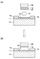
本実施形態の接合体の製造方法の一例を図1に示す。
本発明の接合体300は、第1部材101と第2部材102とを有する。ここで、第1部材101と第2部材102のそれぞれの被接合面にニッケル層111,112を備え、更に前記ニッケル層111,112の表面に、亜鉛との反応性が高く亜鉛と合金を生成する金属表面層(以下、単に「金属表面層」と称する場合がある)121,122を備える。
対向する前記金属表面層121,122の間は、Zn系はんだ材料50で接合される。
<Joint and its manufacturing method>
An example of the manufacturing method of the joined body of this embodiment is shown in FIG.
The joined
The metal surface layers 121 and 122 facing each other are joined with a Zn-based
(Zn系はんだ材料)
亜鉛を主成分とするはんだ材料(Zn系はんだ材料)とは、Znを50質量%以上含むものをいう。
(Zn solder material)
A solder material mainly composed of zinc (Zn-based solder material) refers to a material containing 50% by mass or more of Zn.
具体的に、Zn系はんだ材料50としては、Zn単体、Zn−Al合金、Zn(1−x−y)AlxMyで表される合金、更には、これらにGe、Mg、Sn、In、P等の1種類を添加したもの、或いは2種類以上を組み合わせて添加したものを挙げることができる。
本発明では、Znに起因する問題が解決されるので、Znは単体であっても合金であっても、或いは添加物が含まれていても、同様の効果を奏することができる。
Specifically, the Zn based
In the present invention, since the problem due to Zn is solved, the same effect can be obtained regardless of whether Zn is a simple substance, an alloy, or an additive.
ここで、Zn単体の融点は約420℃である。約420℃での接合も可能であるが、接合部材への熱によるダメージを考慮して、これよりも融点を低くすることも好適な態様である。 Here, the melting point of Zn alone is about 420 ° C. Joining at about 420 ° C. is also possible, but considering the damage to the joining member due to heat, it is also a preferred embodiment to lower the melting point.
融点を降下させるには、ZnにAlを添加して、ZnとAlの合金とすることが好ましい。また、ZnとAlの他に、2質量%以下の金属Mを含有してもよい。すなわち、Zn(1−x−y)AlxMyで表される合金を適用することが好ましい。 In order to lower the melting point, it is preferable to add Al to Zn to form an alloy of Zn and Al. In addition to Zn and Al, 2% by mass or less of metal M may be contained. That is, it is preferable to apply the alloy represented by Zn (1-x-y) Al x M y.
Zn(1−x−y)AlxMyで表される合金において、Alの含有率(xの範囲)は、好ましくは、2質量%以上10質量%以下であり、3質量%以上8質量%以下であることがより好ましい。
AlとMを含まないZn単体(xとyが0の場合)では、上述のように融点が約420℃であって、Alの含有率が増加するに従い、溶解終了温度(液相線温度)は徐々に降下し、Alの含有率が約2質量%で溶解終了温度(液相線温度)が約410℃となり、Alの含有率が約4〜6質量%で液相線温度が約382℃となる。Alの含有率が約6質量%よりも多くなると、溶解し始める温度(固相線温度)と溶解の完了する温度(液相線温度)との差が大きくなり、Alの含有率が10質量%の場合には、固相線温度が約382℃で、液相線温度が約410℃となる。Alの含有率が10質量%よりも多くなると固相線温度と液相線温度との温度差が30℃よりも大きくなるので作業性が低下し、はんだによって接合する際に、位置ずれや接合部材の傾斜等の不具合を発生させやすくなる。
In Zn (1-x-y) alloy represented by Al x M y, the content of Al (range x) is preferably not more than 10 wt% or more 2 wt%, 3 wt% or more and 8 mass % Or less is more preferable.
In the Zn simple substance not containing Al and M (when x and y are 0), the melting point is about 420 ° C. as described above, and as the Al content increases, the melting end temperature (liquidus temperature) Gradually decreases, the melting temperature (liquidus temperature) is about 410 ° C. when the Al content is about 2% by mass, the liquidus temperature is about 382 when the Al content is about 4 to 6% by mass. It becomes ℃. When the Al content exceeds about 6% by mass, the difference between the temperature at which melting begins (solidus temperature) and the temperature at which dissolution completes (liquidus temperature) increases, and the Al content is 10% by mass. %, The solidus temperature is about 382 ° C. and the liquidus temperature is about 410 ° C. When the Al content exceeds 10% by mass, the temperature difference between the solidus temperature and the liquidus temperature becomes larger than 30 ° C., so the workability is reduced, and when the solder is joined, misalignment or joining It becomes easy to generate troubles, such as inclination of a member.
また、Zn(1−x−y)AlxMyで表される合金における金属Mは、亜鉛及びアルミニウム以外の金属を表し、Cuなどを挙げることができる。Cuを2質量%以下含有させると、濡れ性が良好となり密着性が向上する。なおCuを2質量%含有しても液相線温度は殆ど変化しない。
Zn(1−x−y)AlxMyで表される合金において、金属Mの含有量(yの範囲)としては、0〜2質量%であり、好ましくは0〜1.5質量%である。金属Mの含有量が2質量%よりも多くなると、溶解完了までの温度差が30℃よりも大きくなるので作業性が低下し、はんだによって接合する際に、位置ずれや接合部材の傾斜等の不具合が発生し易くなる。
The metal M in the alloy represented by Zn (1-x-y) Al x M y represents a metal other than zinc and aluminum, and the like Cu. When Cu is contained in an amount of 2% by mass or less, the wettability is improved and the adhesion is improved. Even when 2% by mass of Cu is contained, the liquidus temperature hardly changes.
In Zn (1-x-y) alloy represented by Al x M y, the content of the metal M as (range y) is 0 to 2 wt%, preferably 0 to 1.5 mass% is there. When the content of the metal M is more than 2% by mass, the temperature difference until the completion of melting becomes larger than 30 ° C., so that workability is reduced, and when joining with solder, misalignment, inclination of the joining member, etc. Problems are likely to occur.
Zn(1−x−y)AlxMyで表される合金の調製方法は特に制限されず、公知の合金調製方法を適宜適用することができる。 Process for the preparation of Zn (1-x-y) alloy represented by Al x M y is not particularly limited and may be appropriately applying a known alloy preparation method.
Zn(1−x−y)AlxMyで表される合金によって第1部材101と第2部材102とを接合する場合、合金の液相線温度よりも数十℃高い温度で接合することが、接合部を一様に溶融させ、充分な流動性を得る観点から好ましい。例えば、382℃の液相線温度を有するZn(1−x−y)AlxMy合金の場合には、410℃〜440℃程度で接合することが好ましい。
When joining the Zn (1-x-y) and the Al x
その他のZn系はんだ材料としては、特開平11−288955号公報、特開平11−208487号公報、特開平11−172354号公報、特開平11−172353号公報、特開平11−172352号公報、特開2000−208533号公報、特開2000−61686号公報、特開2004−358540号公報、特開2004−358539号公報などのZn系はんだ材料を適用することができる。 Examples of other Zn-based solder materials include JP-A-11-288955, JP-A-11-208487, JP-A-11-172354, JP-A-11-172353, and JP-A-11-172352. A Zn-based solder material such as JP 2000-208533, JP 2000-61686, JP 2004-358540, or JP 2004-358539 can be applied.
(Zn系はんだ材料に対する被接合面)
Zn系はんだ材料50の被接合面には、ニッケル層111,112を備える。ニッケル層111,112を備えることで、Zn系はんだ材料50との界面において不要な反応生成物の生成を抑えることができ、温度変化に対しても耐性が高くなる。
(Surface to be bonded to Zn solder material)
Nickel layers 111 and 112 are provided on the bonded surface of the Zn-based
Zn系はんだ材料50との被接合面に設けるニッケル層111,112の厚みは、0.1μm〜10μmであることが好ましく、0.5μm〜5μmであることがより好ましい。上記の厚さの範囲では、濡れ性の向上に寄与でき、且つ得られた接合体全体に与える熱膨張係数の影響も少ない。
ニッケル層111,112は、スパッタリングやめっき、蒸着等によって形成することができる。
The thickness of the nickel layers 111 and 112 provided on the surface to be joined with the Zn-based
The nickel layers 111 and 112 can be formed by sputtering, plating, vapor deposition, or the like.
更に本発明では、前記ニッケル層111,112の表面に亜鉛との反応性が高く亜鉛と合金を生成する金属表面層(金属表面層)121,122を形成し、Zn系はんだ材料50の濡れ性を改善している。
Further, in the present invention, metal surface layers (metal surface layers) 121 and 122 that are highly reactive with zinc and generate an alloy with zinc are formed on the surfaces of the nickel layers 111 and 112, and the wettability of the Zn-based
ここで、「亜鉛との反応性が高い金属」とは、亜鉛に対して数秒程度で合金を形成するような金属で、その反応量も大きい金属を意味する。具体的には、亜鉛との反応性が高く亜鉛と合金を生成する金属(反応性金属)としては、銅(Cu)、CuNi、CuSn、Ag、Auなどが挙げられる。 Here, the “metal having high reactivity with zinc” means a metal that forms an alloy with zinc in about several seconds and has a large reaction amount. Specifically, copper (Cu), CuNi, CuSn, Ag, Au etc. are mentioned as a metal (reactive metal) which has high reactivity with zinc and produces | generates an alloy with zinc.
特に、金属表面層は銅を主成分とする層(Cu系層)であることが、(1)亜鉛に対する反応性の高さ、(2)Zn系はんだ浴へ溶け込み易く接合後に銅層を消失させることができる、という観点から好適である。 In particular, the metal surface layer is a layer containing copper as a main component (Cu-based layer), (1) high reactivity to zinc, (2) easy to dissolve in the Zn-based solder bath, and the copper layer disappears after joining It is suitable from the viewpoint that it can be made.
銅を主成分とする層(Cu系層)とは、Cuを50質量%以上含む金属層をいう。銅単体であっても銅合金であってもよく、更にこれらに添加物を添加したものであってもよい。銅合金としては、Cu−Au、Cu−Ag、Cu−Ni、Cu−Snなどを挙げることができる。銅を主成分とする層に添加する添加物としては、亜鉛(Zn)、ニッケル(Ni)、マンガン(Mn)などを挙げることができる。 A layer containing Cu as a main component (Cu-based layer) refers to a metal layer containing 50% by mass or more of Cu. It may be a copper simple substance or a copper alloy, and further may be an additive added to these. Examples of the copper alloy include Cu—Au, Cu—Ag, Cu—Ni, and Cu—Sn. Examples of the additive added to the copper-based layer include zinc (Zn), nickel (Ni), and manganese (Mn).
Cu系層は、より好ましくはCuを65質量%以上含む金属層であり、更に好ましくはCuを80質量%以上含む金属層である。 The Cu-based layer is more preferably a metal layer containing 65% by mass or more of Cu, and still more preferably a metal layer containing 80% by mass or more of Cu.
Znは濡れ性の低い物質であり、Niに対しても濡れ拡がり難い。はんだ材料が接合の加熱時に濡れ拡がらないと、均一に接合することができず、被接合部材が傾いた状態で接合してしまうなど、不具合を発生させる場合がある。 Zn is a substance with low wettability, and it is difficult for it to spread even with Ni. If the solder material does not wet and spread during the heating of bonding, bonding cannot be performed uniformly, and problems may occur such as bonding with the members to be bonded tilted.
このような不具合を解消するため、従来の方法では、接合の加熱時に被接合部材に外圧を加えながら擦動させて、均一に且つ被接合部材が傾かないように接合していた。このような方法を採用すれば、Zn系はんだ材料であっても、被接合部材を均一に接合することができる。しかし、加熱しながら外圧を加えることは、作業上煩雑な操作である上に、周辺部にはんだ材料がはみ出し、電気的な不具合を生じる恐れがある。 In order to solve such a problem, in the conventional method, the members to be joined are rubbed while applying external pressure during the heating of joining, and the members to be joined are joined so as not to tilt. By adopting such a method, the members to be joined can be uniformly joined even with a Zn-based solder material. However, applying external pressure while heating is a cumbersome operation, and the solder material may protrude from the peripheral portion, which may cause electrical problems.
そこで、本発明では、溶融したZnと反応して合金を作り易い金属(反応性金属)をZn系はんだ材料50の接合面に設けることで、Zn系はんだ材料50の濡れ性を向上させている。詳細には、接合時の加熱において、Zn系はんだ材料50が融点を超えて溶融した際に、Zn系はんだ材料50は、反応性金属と合金の生成反応を起こしながら反応性金属を求めて自ら拡がるという現象を利用している。
Therefore, in the present invention, the wettability of the Zn-based
一方で、濡れ性を向上させるために形成した前記金属表面層121,122が、はんだ接合後も残存すると、パワー半導体モジュールを製品として使用する際に、冷熱サイクルによってZnと反応性金属とで不要な反応生成物を生成させる場合がある。
そのような不要な反応生成物は、通常、脆い物質であったり、硬い物質であったりするので、その不要な反応生成物の存在する位置を起点にクラックが発生し、その結果、接合部材のクラックの発生や接合界面から生じる剥離などの不具合を発生させ易い。
そこで、金属表面層121,122は、はんだ材料が濡れ拡がった後は、Znのはんだ浴中に取り込み消失させる。
On the other hand, if the metal surface layers 121 and 122 formed to improve wettability remain after soldering, it is not necessary to use Zn and reactive metals by a thermal cycle when using the power semiconductor module as a product. Reaction products may be produced.
Such an unnecessary reaction product is usually a brittle substance or a hard substance, so that a crack is generated starting from the position where the unnecessary reaction product exists. It is easy to generate defects such as cracks and peeling that occurs from the bonding interface.
Therefore, the metal surface layers 121 and 122 are taken into the Zn solder bath and disappear after the solder material wets and spreads.
はんだ材料が濡れ拡がった後の接合界面で、金属表面層121,122が消失するような金属表面層121,122の厚さは、はんだ接合時の加熱温度や加熱時間、更にははんだ材料の種類などによって異なるため、一概に決めることはできず、適宜好適な膜厚を採用することが望ましい。
しかしながら、概ね、3nm以上1000nm以下であることが好ましく、10nm以上200nm以下であることが好ましい。膜厚が薄すぎると、接合部分が島状となり均一に接合することができない場合がある。一方、1000nmよりも厚い場合には、Zn系はんだ浴中に全てが取り込まれず、金属表面層121,122が残存する場合がある。
The thicknesses of the metal surface layers 121 and 122 at which the metal surface layers 121 and 122 disappear at the bonding interface after the solder material has spread and spread are the heating temperature and heating time at the time of solder bonding, and the type of the solder material. Therefore, it is not possible to make a general decision, and it is desirable to adopt a suitable film thickness as appropriate.
However, it is generally preferably 3 nm or more and 1000 nm or less, and more preferably 10 nm or more and 200 nm or less. If the film thickness is too thin, the bonded portion may be island-shaped and cannot be bonded uniformly. On the other hand, when it is thicker than 1000 nm, not all is taken into the Zn-based solder bath, and the metal surface layers 121 and 122 may remain.
金属表面層121,122は、スパッタリングやめっき、蒸着等によって形成することができる。 The metal surface layers 121 and 122 can be formed by sputtering, plating, vapor deposition, or the like.
(接合体の製造方法)
図1(A)に示すように、第1部材101と第2部材102のそれぞれの表面にニッケル層111,112を形成する。更に、ニッケル層111,112の上に、金属表面層121,122を形成する。
次に、図1(A)に示すように、第1部材101と第2部材102におけるそれぞれの金属表面層121,122が対向するように配置し、その間にZn系はんだ材料50を挟み、第1部材101/ニッケル層111/金属表面層121/Zn系はんだ材料50/金属表面層122/ニッケル層112/第2部材102をこの順に積層した状態で、リフロー法等を利用して接合して、接合体300を形成する。
(Method of manufacturing joined body)
As shown in FIG. 1A, nickel layers 111 and 112 are formed on the surfaces of the
Next, as shown in FIG. 1A, the metal surface layers 121 and 122 of the
接合は、Zn系はんだ材料50の融点よりも30℃〜60℃程度高い温度で行うことが好ましい。また、接合は、不活性ガス又は還元ガス雰囲気下で行なう。
The joining is preferably performed at a temperature about 30 ° C. to 60 ° C. higher than the melting point of the Zn-based
被接合面の表面に設けられた金属表面層121,122は非常に薄く、Zn系はんだ材料50の体積に比べて桁違いに少ない。そのため、接合時の加熱により溶融したZn系はんだ材料50のはんだ浴の中に金属表面層121,122が取り込まれて、結果、図1(B)に示すように、金属表面層121,122は接合界面には残存しない。
The metal surface layers 121 and 122 provided on the surfaces to be joined are very thin and are much smaller than the volume of the Zn-based
その結果、Zn系はんだ材料50は、ニッケル層111,112と接する。この状態で冷熱サイクルに曝されても、NiとZnとは不要な反応生成物を生成させ難い。したがって、接合界面で不要な反応生成物を生成させにくく、反応生成物を起点としたクラックの発生が防止でき、界面での剥離などの不具合の発生が抑えられる。
As a result, the Zn-based
形成された接合部501の層の厚さは、熱伝導及び熱応力の観点から5μm以上500μm以下であることが好ましく、10μm以上200μm以下であることがより好ましい。
The thickness of the formed
図2では、接合によって濡れ拡がったZn系はんだ材料50の状態を説明する。第1部材101と第2部材102の形状や大きさに特に制限はないが、図2では、第1部材101の被接合面が、第2部材102の被接合面よりも大きい場合で説明する。
In FIG. 2, the state of the Zn-based
図2(A)は接合前の状態を示し、図2(B)は接合後の状態を示す。
本発明においてはZnの濡れ性が向上しているため、図2(B)に示すように、接合の加熱によってはんだ材料が均一に濡れ拡がり、はんだ材料はフィレットと呼ばれる裾拡がりの形状となる場合がある。このような接合形状であっても均一に接合しているのであれば問題ないが、フィレットの拡がりを抑制する方法としては、以下の方法を例示することができる。
2A shows a state before joining, and FIG. 2B shows a state after joining.
In the present invention, since the wettability of Zn is improved, as shown in FIG. 2B, the solder material uniformly spreads by heating of the joint, and the solder material has a hem-spread shape called a fillet. There is. Even if it is such a joining shape, there is no problem as long as it is uniformly joined, but the following method can be exemplified as a method for suppressing the spread of the fillet.
例えば、図3(A)(B)に示すように、第1部材101に設ける金属表面層121の面積を第1部材101の被接合面よりも小さくする方法が挙げられる。
所望の面積の金属表面層121を形成するには、絶縁基板上にマスキングシートなどを貼ってメッキしたり、或いは、開口部を有するマスク部材を装着してスパッタリングしたりすればよい。したがって、この方法では簡易な方法で、はんだ材料の濡れ拡がる面積を制御することができる。
For example, as shown in FIGS. 3A and 3B, there is a method in which the area of the
In order to form the
なお、本発明の技術は、濡れ性に最も影響のある界面の状態を直接的に変えるので、図3に示すように、はんだ材料の濡れ拡がる範囲を制御することが容易である。
これに対して、従来のように、はんだ材料に他の物質を添加して濡れ性を向上させる方法では、濡れ性に直接影響を及ぼす界面のみならず、はんだ材料全体も改質されているので、はんだ材料が濡れ拡がる範囲を制御することは、本発明に比べて困難である。
The technique of the present invention directly changes the state of the interface that has the most influence on wettability. Therefore, as shown in FIG. 3, it is easy to control the range in which the solder material spreads.
In contrast, the conventional method of adding other substances to the solder material to improve the wettability improves not only the interface that directly affects the wettability but also the entire solder material. It is difficult to control the range in which the solder material spreads out compared to the present invention.
また、図4(A)(B)に示すように、予めはんだ材料の拡がりを抑止する部分にレジスト70等をパターニングしておくことで、はんだ材料の濡れ拡がりを制御することができる。
接合後に不要なレジストを除去することも可能であり、耐熱性の高いレジストの場合には、そのまま残存させてもよい。
Further, as shown in FIGS. 4A and 4B, the wetting and spreading of the solder material can be controlled by patterning the resist 70 and the like in advance in a portion where the spreading of the solder material is suppressed.
It is possible to remove unnecessary resist after bonding, and in the case of a resist having high heat resistance, it may be left as it is.
なお、Zn系はんだ材料50で接合した後の接合面では、金属表面層121,122が消失している。しかし、図2(B)に示すように、金属表面層121,122が残存している領域Aが確認できれば、本発明の方法を適用したか否かは確認可能である。
Note that the metal surface layers 121 and 122 have disappeared on the joint surface after joining with the Zn-based
<パワー半導体モジュール及びその製造方法>
本発明のパワー半導体モジュールは、パワー半導体素子と絶縁基板と放熱板とを有する。更に、前記パワー半導体素子と前記絶縁基板との間の第一接合部、及び前記絶縁基板と前記放熱板との間の第二接合部を有する。
本発明では、第一接合部及び第二接合部の少なくとも一方が、上述のZn系はんだ材料で接合されていればよく、第一接合部及び第二接合部の両者がZn系はんだ材料で接合されていてもよい。
<Power semiconductor module and manufacturing method thereof>
The power semiconductor module of the present invention includes a power semiconductor element, an insulating substrate, and a heat sink. Furthermore, it has the 1st junction part between the said power semiconductor element and the said insulated substrate, and the 2nd junction part between the said insulated substrate and the said heat sink.
In the present invention, it is sufficient that at least one of the first joint and the second joint is joined by the above-described Zn-based solder material, and both the first joint and the second joint are joined by the Zn-based solder material. May be.
更に、本発明では、Zn系はんだ材料によって接合する被接合面には、ニッケル層を備え、更に、前記ニッケル層の表面に金属表面層(望ましくはCu系層)を備える。金属表面層は、Zn系はんだ材料で接合した後で消失していることが望ましい。 Furthermore, in the present invention, a surface to be joined by a Zn-based solder material is provided with a nickel layer, and further, a metal surface layer (preferably a Cu-based layer) is provided on the surface of the nickel layer. It is desirable that the metal surface layer disappears after joining with the Zn-based solder material.
上記の構成のパワー半導体モジュールとすることで、パワー半導体モジュールの接合部分における耐熱性が向上し、緻密に接合される。また被接合部材どうしが傾斜して接合するなどの不具合の発生が抑えられたパワー半導体モジュールとなる。 By setting it as the power semiconductor module of said structure, the heat resistance in the junction part of a power semiconductor module improves, and it joins densely. Moreover, it becomes a power semiconductor module with which generation | occurrence | production of malfunctions, such as to-be-joined members inclined and joined, was suppressed.
なお、本発明のパワー半導体モジュールでは、Zn系はんだ材料を、第一接合部及び第二接合部のいずれに適用してもよく、また、第一接合部を先に接合し次に第二接合部を接合してもよいし、第二接合部を先に接合した後、第一接合部を接合してもよい。 In the power semiconductor module of the present invention, the Zn-based solder material may be applied to either the first joint or the second joint, and the first joint is joined first and then the second joint. The parts may be joined, or the first joined part may be joined after the second joined part is joined first.
しかし、いずれにしても2回目のはんだ付けの温度が、1回目に用いたはんだ材料の融点よりも高いと、2回目のはんだ付けの際に1回目にはんだ付けした部分が溶融して、位置ずれを起こしたり傾斜したりといった不具合を発生させてしまう。 However, in any case, if the temperature of the second soldering is higher than the melting point of the solder material used for the first time, the portion soldered for the first time will be melted during the second soldering. It will cause problems such as misalignment and tilting.
この問題を回避するため、一般的に、1回目に用いるはんだ材料の融点は、2回目に用いるはんだ材料の融点よりも高くなるように、はんだの材料を選択する。好適には、2回目の接合に用いるはんだ材料の融点は、1回目の接合に用いるはんだ材料の融点よりも30℃以上低いことが望ましい。 In order to avoid this problem, the solder material is generally selected so that the melting point of the solder material used for the first time is higher than the melting point of the solder material used for the second time. Preferably, the melting point of the solder material used for the second bonding is preferably 30 ° C. or lower than the melting point of the solder material used for the first bonding.
つまり1回目の接合に、融点が約380〜420℃のZn系はんだ材料を適用した場合、2回目の接合に用いるはんだ材料は、Zn系はんだ材料の融点よりも30℃以上低い融点を有するものとすることが好ましい。一方で、パワー半導体からの発熱を考慮すると、2回目の接合に用いるはんだ材料の融点は200℃以上であることが望ましい。よって、1回目の接合に、Zn系はんだ材料を適用した場合には、2回目の接合に用いるはんだ材料は、融点が210℃〜350℃程度のものを適用することが好ましい。 That is, when a Zn-based solder material having a melting point of about 380 to 420 ° C. is applied to the first bonding, the solder material used for the second bonding has a melting point that is 30 ° C. lower than the melting point of the Zn-based solder material It is preferable that On the other hand, considering the heat generation from the power semiconductor, it is desirable that the melting point of the solder material used for the second bonding is 200 ° C. or higher. Therefore, when a Zn-based solder material is applied to the first joining, it is preferable to apply a solder material having a melting point of about 210 ° C. to 350 ° C. for the second joining.
他方、2回目の接合に、Zn系はんだ材料を適用した場合には、1回目の接合に用いるはんだ材料は、Zn系はんだ材料の融点よりも30℃以上高い固相線温度を有するものであることが好ましい。一方で、はんだ付けの際の加熱によって半導体素子が破壊されるのを防ぐには、融点が650℃以下、好ましくは450℃以下であることが好ましい。よって、2回目の接合にZn系はんだ材料を適用した場合には、1回目の接合に用いるはんだ材料は、融点が450〜650℃のものを適用することが好ましい。 On the other hand, when a Zn-based solder material is applied to the second bonding, the solder material used for the first bonding has a solidus temperature higher by 30 ° C. than the melting point of the Zn-based solder material. It is preferable. On the other hand, in order to prevent the semiconductor element from being destroyed by heating during soldering, the melting point is preferably 650 ° C. or less, and preferably 450 ° C. or less. Therefore, when a Zn-based solder material is applied to the second bonding, it is preferable to apply a solder material having a melting point of 450 to 650 ° C. for the first bonding.
上記から、Zn系はんだ材料は、その融点が約380〜420℃であるという観点から1回目の接合に用いることが好ましく、2回目の接合に用いるはんだ材料は、210℃〜350℃程度の融点を有する材料を適用することが好ましい。 From the above, the Zn-based solder material is preferably used for the first bonding from the viewpoint that the melting point is about 380 to 420 ° C., and the solder material used for the second bonding has a melting point of about 210 ° C. to 350 ° C. It is preferable to apply a material having
このような条件下で、2回目の接合に用いるはんだ材料としては、Bi系はんだ材料(融点:約270℃)やAu系はんだ材料(融点:約280℃)、Sn−Sb系はんだ材料(融点:約250℃)などを挙げることができる。これらの中でも、2回目の接合に用いるはんだ材料としては、Bi系はんだ材料を適用することが、貴金属を用いないというコスト面、安全性の観点から好適である。 Under such conditions, the solder material used for the second bonding includes a Bi solder material (melting point: about 270 ° C.), an Au solder material (melting point: about 280 ° C.), and a Sn—Sb solder material (melting point). : About 250 ° C.). Among these, as the solder material used for the second bonding, it is preferable to use a Bi-based solder material from the viewpoint of cost and safety that no precious metal is used.
なお、大量の熱を発する半導体素子に近い側の第一接合部には、融点の高いZn系はんだ材料を適用し、半導体素子から遠い側の第二接合部には、Bi系はんだ材料等、Zn系はんだ材料よりも融点の低いはんだ材料を適用することが好適である。 In addition, a Zn-based solder material having a high melting point is applied to the first joint portion close to the semiconductor element that emits a large amount of heat, and a Bi-based solder material or the like is applied to the second joint portion far from the semiconductor element. It is preferable to apply a solder material having a melting point lower than that of the Zn-based solder material.
したがって、以下、図5に示す第一の実施形態では、第一接合部にはZn系はんだ材料を適用し、第二接合部にはその他のはんだ材料を適用する場合について説明する。 Therefore, hereinafter, in the first embodiment shown in FIG. 5, a case where a Zn-based solder material is applied to the first joint and another solder material is applied to the second joint will be described.
[第一の実施形態のパワー半導体モジュール]
図5に、第一の実施形態のパワー半導体モジュール10の要部断面図を模式的に示す。
パワー半導体モジュール10は、パワー半導体素子20と絶縁部30と放熱板40とを有する。パワー半導体素子20と絶縁部30との間は第一接合部500によって接合される。絶縁部30と放熱板40との間は第二接合部600によって接合される。
[Power Semiconductor Module of First Embodiment]
In FIG. 5, the principal part sectional drawing of the
The
パワー半導体モジュール10は、車載用インバータなどに用いられるものである。パワー半導体モジュール10の周辺には図示しない内燃機関が設けられているために、パワー半導体モジュール10が置かれている環境はかなりの高温となっている。さらに、パワー半導体素子として次世代のGaNやSiCを用いた場合には、パワー半導体素子20からの発熱が大きく、パワー半導体モジュール10の温度が上昇する。
The
パワー半導体素子20が自身の発する熱や高温の周囲環境によって破壊するのを防ぐよう、冷却水が流動する冷却管(図示せず)が設けられ、冷却管とパワー半導体素子20との間に放熱板40が設けられる。
A cooling pipe (not shown) through which cooling water flows is provided to prevent the
したがって、一般的にパワー半導体モジュールに求められる性能としては、第一に、冷却と発熱を繰り返す冷熱サイクルに対して、半導体や絶縁基板など被接合部材の亀裂、接合部分のクラックの発生や、接合界面から生じる剥離などの不具合を生じさせないことであり、第二に、絶縁基板によって確実に絶縁させることであり、第三にパワー半導体素子から発せられた熱を放熱板までなるべく蓄積することなく伝えることである。 Therefore, the performance generally required for a power semiconductor module is as follows. First, with respect to a cooling cycle in which cooling and heat generation are repeated, a crack in a bonded member such as a semiconductor or an insulating substrate, a crack in a bonded portion, or a bonding Second, it must be insulated by an insulating substrate, and third, heat generated from the power semiconductor element can be transmitted to the heat sink without accumulating as much as possible. That is.
冷熱サイクルに対して上記亀裂、クラック、剥離などを発生させないためには、半導体素子20、絶縁基板30、放熱板40及び接合部500,600などの部材そのものが温度変化に対して耐久性がなければならず、加えて、冷熱サイクルにおいて、接合界面に不要な反応生成物が発生したり、この反応生成物が大きく成長しないことが重要である。かかる反応生成物は脆い物質であったり、逆に硬すぎる物質であったりして、反応生成物が発生した部位を起点として接合部材のクラックの発生や接合界面から生じる剥離等を起こしやすい。
In order to prevent the above-described cracks, cracks, peeling, etc. from occurring in the cooling and heating cycle, the members such as the
また、各部材の熱膨張係数が近い値であることも、冷熱サイクルによる上記亀裂やクラック、剥離などの発生を抑制するのに重要である。熱膨張係数が全く異なる部材を接合すると、冷熱サイクルによって繰り返し起こる部材の体積変化によって、上記亀裂やクラック、剥離等を発生させやすくなる。 Moreover, it is important for the thermal expansion coefficient of each member to be a close value to suppress the occurrence of the cracks, cracks, peeling, and the like due to the thermal cycle. When members having completely different thermal expansion coefficients are joined, the above-described cracks, cracks, peeling, and the like are likely to occur due to the volume change of the member repeatedly caused by the cooling and heating cycle.
パワー半導体モジュールの接合部分に対して求められる性能としては、第一に、冷熱サイクルに対して半導体や絶縁基板の亀裂、接合部材のクラックの発生や、接合界面から生じる剥離などの不具合を生じさせないことであり、第二に、接合が均一に行われ、部材が傾斜して接合されないことである。 The performance required for the joint part of the power semiconductor module is that, firstly, it does not cause defects such as cracks in the semiconductor and insulating substrate, cracks in the joining member, and delamination from the joining interface in the thermal cycle. Secondly, the joining is performed uniformly and the members are not inclined and joined.
第一の実施形態のパワー半導体モジュールでは、第一接合部500にZn系はんだ材料50を適用して接合しているため、接合部分の耐熱性は高くなっている。
また、Zn系はんだ材料50が接する界面には金属表面層24,39が設けられているので、被接合面に対するZn系はんだ材料50の濡れ性が向上している。その結果、接合が均一に行われるので、部材が傾斜して接合される等の不具合を発生させず、また、熱伝導が阻害されるのを防ぐことができる。
In the power semiconductor module of the first embodiment, since the Zn-based
In addition, since the metal surface layers 24 and 39 are provided at the interface where the Zn-based
一方で、接合後のパワー半導体モジュールでは、Zn系はんだ材料50が接する部分においては、はんだ浴中に金属表面層24,39が取り込まれて、金属表面層24,39は消失している。
反応性金属が亜鉛(Zn)と接した状態で残存していると、パワー半導体モジュールを製品として使用している間に半導体素子から発せられる熱によって、反応性金属と亜鉛(Zn)とが反応し、不要な反応生成物を生成することがある。
これに対して、Zn系はんだ材料50が接する部分において、Znはんだ浴中に反応性金属が取り込まれて金属表面層24,39が消失していれば、Znと反応性金属とによる不要な反応生成物を生じることなく強固に接合する。その結果、反応生成物の生成に起因した上記クラックや剥離などの不具合の発生が抑制される。
On the other hand, in the power semiconductor module after bonding, the metal surface layers 24 and 39 are taken into the solder bath at the portion where the Zn-based
If the reactive metal remains in contact with zinc (Zn), the reactive metal reacts with zinc (Zn) due to the heat generated from the semiconductor element while the power semiconductor module is used as a product. In some cases, unnecessary reaction products may be produced.
On the other hand, if the reactive metal is taken into the Zn solder bath and the metal surface layers 24 and 39 disappear in the portion where the Zn-based
この場合、金属表面層24,39は、Znと接している部分において消失していればよく、Zn系はんだ材料50が接していない部分については、残存していても構わない。
In this case, the metal surface layers 24 and 39 only have to disappear in the portions in contact with Zn, and the portions not in contact with the Zn-based
更に、本発明では、被接合面にニッケル層22,38を設けているため、金属表面層24,39が消失した後には、ニッケル層22,38とZn系はんだ材料50とが接合している。ZnとNiとの界面では、パワー半導体モジュールを製品として使用したときに半導体素子から発せられる熱によっても、不要な反応生成物を生成させない。その結果、不要な反応生成物に因るクラックの発生や接合界面での剥離の発生を抑制することができる。
Furthermore, in the present invention, since the nickel layers 22 and 38 are provided on the surfaces to be joined, the nickel layers 22 and 38 and the Zn-based
なお、図5のパワー半導体モジュールでは、金属表面層24、39を点線で図示しているが、第一接合部500では、これらの金属表面層24、39は消失している。
更に、パワー半導体モジュールの各部材について、詳細に説明する。
In the power semiconductor module of FIG. 5, the metal surface layers 24 and 39 are illustrated by dotted lines, but at the first
Furthermore, each member of the power semiconductor module will be described in detail.
(第一接合部)
本発明における第一接合部500は、パワー半導体素子20と絶縁部30との間を接合するために設けられる。第一接合部500では、上述のZn系はんだ材料50を適用する。
(First joint)
The
Zn系はんだ材料50の被接合面には、ニッケル層を備える。第一の実施形態では、第一接合部500にZn系はんだ材料50を適用するので、パワー半導体素子20と絶縁部30のそれぞれの被接合面にニッケル層22,38を備える。ニッケル層22,38を備えることで、Zn系はんだ材料50との界面において不要な反応生成物の生成を抑えることができ、温度変化に対しても耐性が高くなる。
A surface to be joined of the Zn-based
Zn系はんだ材料50との被接合面に設けるニッケル層22,38の厚みは、0.1μm〜10μmであることが好ましく、0.5μm〜5μmであることがより好ましい。0.1μmよりも薄いと、接合時にはんだ材料に溶け込み消失する恐れがあり、10μmよりも厚いと、パワー半導体モジュール全体の熱膨張係数に影響を与え、熱応力を生じさせるようになるため好ましくない。
ニッケル層22,38は、スパッタリングやめっき、蒸着等によって形成することができる。
The thickness of the nickel layers 22 and 38 provided on the surface to be joined with the Zn-based
The nickel layers 22 and 38 can be formed by sputtering, plating, vapor deposition, or the like.
更に本発明では、前記ニッケル層22,38の表面に金属表面層24,39を形成し、Zn系はんだ材料50の濡れ性を改善している。前記接合体で説明した通り、金属表面層24,39としては、銅を主成分とする層(Cu系層)であることが好ましい。
Furthermore, in the present invention, the metal surface layers 24 and 39 are formed on the surfaces of the nickel layers 22 and 38 to improve the wettability of the Zn-based
本発明では、金属表面層24,39を設けることで、Znの濡れ性を改善し、緻密な接合を実現している。また均一な接合によって、部材が傾斜して接合される等の不具合が抑えられている。
金属表面層24,39は、はんだ材料が濡れ拡がった後は、Znのはんだ浴中に取り込まれ消失している。金属表面層24,39が、はんだ接合後には消失していると、パワー半導体モジュールを製品として使用したときの冷熱サイクルによっても、不要な反応生成物を生成させない。
In the present invention, by providing the metal surface layers 24 and 39, the wettability of Zn is improved and the dense bonding is realized. In addition, due to the uniform bonding, problems such as the members being inclined and bonded are suppressed.
After the solder material wets and spreads, the metal surface layers 24 and 39 are taken into the Zn solder bath and disappear. If the metal surface layers 24 and 39 are lost after the solder joint, unnecessary reaction products are not generated even by a cooling and heating cycle when the power semiconductor module is used as a product.
はんだ材料が濡れ拡がった後の接合界面で、金属表面層24,39が消失するような金属表面層24,39の厚さは、はんだ接合時の加熱温度や加熱時間、更にははんだ材料の種類などによって異なるため、一概に決めることはできず、適宜好適な膜厚を採用することが望ましい。
しかしながら、概ね、3nm以上1000nm以下であることが好ましく、10nm以上200nm以下であることが好ましい。膜厚が薄すぎると、接合部分が島状となり均一に接合することができない場合がある。一方、1000nmよりも厚い場合には、Zn系はんだ浴中に全てが取り込まれず、金属表面層24,39が残存する場合がある。
The thickness of the metal surface layers 24 and 39 at which the metal surface layers 24 and 39 disappear at the bonding interface after the solder material has spread and spread is determined by the heating temperature and heating time at the time of solder bonding, and the type of the solder material. Therefore, it is not possible to make a general decision, and it is desirable to adopt a suitable film thickness as appropriate.
However, it is generally preferably 3 nm or more and 1000 nm or less, and more preferably 10 nm or more and 200 nm or less. If the film thickness is too thin, the bonded portion may be island-shaped and cannot be bonded uniformly. On the other hand, when it is thicker than 1000 nm, not all is taken into the Zn-based solder bath, and the metal surface layers 24 and 39 may remain.
金属表面層24,39は、スパッタリングやめっき、蒸着等によって形成することができる。 The metal surface layers 24 and 39 can be formed by sputtering, plating, vapor deposition, or the like.
接合後に形成された第一接合部500の層の厚さは、熱伝導及び熱応力の観点から5μm以上500μm以下であることが好ましく、10μm以上200μm以下であることがより好ましい。 The thickness of the layer of the first joint 500 formed after joining is preferably 5 μm or more and 500 μm or less, more preferably 10 μm or more and 200 μm or less from the viewpoint of thermal conduction and thermal stress.
(第二接合部)
本発明における第二接合部600は、絶縁部30と放熱板40との間を接合するために設けられる。第二接合部600の材質としては特に制限されないが、第一の実施形態では上記第一接合部500に約380〜420℃の融点を有するZn系はんだ材料50を適用するため、製造工程上、210℃〜350℃程度の融点を有する材料を適用することが好ましい。
(Second joint)
The
上記融点を有するはんだ材料としては、Bi系はんだ材料(融点:約270℃)やAu系はんだ材料(融点:約280℃)、Sn−Sb系はんだ材料(融点:約250℃)などを適用することができる。 As the solder material having the melting point, Bi solder material (melting point: about 270 ° C.), Au solder material (melting point: about 280 ° C.), Sn—Sb solder material (melting point: about 250 ° C.), or the like is applied. be able to.
Bi系はんだ材料としては、Bi単体のほかに、BiにCu、Ni、Agなどを添加したものを挙げることができるが、下記(1)〜(4)に記載のBi系はんだ材料であることが固相線温度を低下させない観点から好ましい。
更に、下記(1)〜(4)に記載のBi系はんだ材料の中でも、Biの脆性を解消して機械的強度を高める観点からは、下記(2)〜(4)のBi系はんだ材料であることが好ましい。
Examples of the Bi-based solder material include those obtained by adding Cu, Ni, Ag, etc. to Bi in addition to Bi alone, and are Bi-based solder materials described in (1) to (4) below. Is preferable from the viewpoint of not lowering the solidus temperature.
Furthermore, among the Bi-based solder materials described in the following (1) to (4), from the viewpoint of eliminating the brittleness of Bi and increasing the mechanical strength, the Bi-based solder materials of the following (2) to (4) are used. Preferably there is.
(1)Bi単体
(2)Bi中にCuAlMn合金粒子を分散させたBi−CuAlMn
(3)BiにCuを添加した材料
(4)BiにNiを添加した材料
(1) Bi simple substance (2) Bi-CuAlMn in which CuAlMn alloy particles are dispersed in Bi
(3) Material in which Cu is added to Bi (4) Material in which Ni is added to Bi
また、Au系はんだ材料としては、Au−20Sn(融点280℃)、Au−3Si(融点363℃)、Au−12.5Ge(融点361℃)などを挙げることができる。 Examples of Au-based solder materials include Au-20Sn (melting point 280 ° C.), Au-3Si (melting point 363 ° C.), Au-12.5Ge (melting point 361 ° C.), and the like.
Sn−Sb系はんだ材料としては、Sn−5Sb(融点236℃)、Sn−9Sb(融点246℃)などを挙げることができる。 Examples of the Sn—Sb solder material include Sn-5Sb (melting point 236 ° C.) and Sn-9Sb (melting point 246 ° C.).
(パワー半導体素子)
パワー半導体素子20としては、特に制限することなく用途に応じて適宜適用することができ、一般的なSi基板なども適用できる。
本発明では、次世代素子としてGaN基板やSiC基板などを用いた場合であっても、第一接合部500に用いるZn系はんだ材料50の融点(固相線温度)が約380〜420℃のため、半導体素子の繰り返し使用によって放熱される200℃を超える高温に対しても、亀裂や剥離などの不具合を生じさせない信頼性の高いパワー半導体モジュールとなる。
(Power semiconductor element)
As the
In the present invention, the melting point (solidus temperature) of the Zn-based
第一の実施形態では、第一接合部500にZn系はんだ材料50を適用するので、パワー半導体素子20は、第一接合部500側の表面にニッケル層22を設ける。第一接合部500としてZn系はんだ材料50を用いた場合、Zn系はんだ材料50とニッケル層22との界面においては、冷熱サイクルによる不要な生成物を発生させることがないので、温度変化に対しても耐性が高くなる。
In the first embodiment, since the Zn-based
更にニッケル層22の表面には、上述の通り、金属表面層24が設けられる。この金属表面層24は接合時にはんだ浴に溶け込み、はんだ材料が濡れ拡がった後のZn系はんだ材料50との界面では、金属表面層24は残存しないことが望ましい。
Furthermore, the
(絶縁部)
絶縁部30における絶縁基板32としては、絶縁性を確保できるものであれば特に制限されず適用することができるが、好ましくは冷却サイクル時に顕著な熱応力を生じさせないよう、半導体素子の熱膨張係数と同程度の熱膨張係数を有するものである。
(Insulation part)
The insulating
具体的に好適な絶縁基板32としては、AlN、Si3N4、Al2O3などで形成されるものを挙げることができ、この中でも熱伝導率及び熱膨張係数の観点から、Si3N4又はAlNが好適である。更に、Si3N4の破壊強度はAlNの破壊強度よりも高く、絶縁部材自体の寿命が長くなることから、絶縁基板32としてはSi3N4であることがより好適である。
Specific examples of the insulating
また、絶縁基板32におけるパワー半導体素子側の表面から半導体素子に電気を通すために絶縁基板32の表面に導電層34を設ける。また、温度変化に対するそりを抑制するために、放熱板40側にも導電層36を設けることが好ましい。
Further, a
絶縁基板32としてAlNのセラミックスを用いる場合には、導電層34、36としては、Al、Cu、Mo、Niなどが好適であり、この中でもAl及びCuが好ましい。AlNの表面にAl層を設けると、温度変化に対して塑性変形を生じ、熱応力を緩和でき、Cu層を設けると導電率が高いことから薄くすることができ、熱応力を緩和できるため好適である。
つまり、AlNのセラミックスを絶縁基板32として適用する場合には、絶縁部30としては、Cu/AlN/Cu積層体又はAl/AlN/Al積層体であることが好ましい。
In the case of using AlN ceramics as the insulating
That is, when AlN ceramics are applied as the insulating
一方、絶縁基板32としてSi3N4のセラミックスを用いる場合には、導電層34、36としては、Al、Cu、Mo、Niなどが好適であり、この中でもAl及びCuが好ましく、Cuであることがより好ましい。Cuは導電率が高いことからCu層を設けると導電率が高いことから薄くすることができ、熱応力を緩和できるため好適である。また、Cu/Si3N4/Cu積層体は、冷熱サイクル試験においても破壊され難く、絶縁部30としての信頼性が高い。
On the other hand, when Si 3 N 4 ceramics is used as the insulating
絶縁基板32に備える導電層34、36の厚さは、0.01mm〜1mmであることが好ましく、0.05mm〜0.6mmであることがより好ましい。導電層34、36の厚さが0.01mm未満の場合には、導電層の延在方向での電流による損失及び発熱が無視できなくなり、1mmを超える場合には、パワー半導体モジュール全体の熱膨張係数に影響を与え、熱応力を生じさせるようになるため好ましくない。
The thickness of the
絶縁基板32の両表面に導電層34、36を貼付する方法は特に制限されず、ロウ付けなどの公知の方法を適宜採用することができる。
A method for attaching the
Zn系はんだ材料50を適用する第一接合部500側の絶縁部30の表面には、ニッケル層38を設ける。上述の通り、Zn系はんだ材料50は、ニッケル層との界面においては、冷熱サイクルによる不要な生成物を発生させることがないので、ニッケル層38を設けることで温度変化に対しても亀裂や剥離などの不具合を生じさせない。
A
ニッケル層38の厚みは、0.1μm〜10μmであることが好ましく、3μm〜8μmであることがより好ましい。0.1μmよりも薄いと、接合時にはんだ材料に溶け込み消失する恐れがあり、10μmよりも厚いと、パワー半導体モジュール全体の熱膨張係数に影響を与え、熱応力を生じさせるようになるため好ましくない。
The thickness of the
更にニッケル層38の表面には、上述の通り、金属表面層39が設けられる。この金属表面層39は接合時にはんだ浴に溶け込み、はんだ材料が濡れ拡がった後のZn系はんだ材料50との界面では、金属表面層39は残存しない。
Further, the
第二接合部600側の絶縁部30の表面には、第二接合部600のはんだ材料に応じて、金属膜を適宜設けることもできる。
A metal film can be appropriately provided on the surface of the insulating
(放熱板)
放熱板40としては、放熱性を有するものであれば特に制限されず適用することができるが、熱伝導率が充分高く放熱板としての機能に優れ、また半導体素子の熱膨張係数に近いものを用いることが好ましい。
(Heatsink)
The heat sink 40 can be applied without particular limitation as long as it has heat dissipation properties, but it has a sufficiently high thermal conductivity and an excellent function as a heat sink and is close to the thermal expansion coefficient of the semiconductor element. It is preferable to use it.
具体的に好適な放熱板40としては、Mo、Cu−Mo合金、Al−SiC、Cu、Alなどで形成されるものを挙げることができ、この中でも高い熱伝導率とパワー半導体素子に近い熱膨張係数を有することから、Moが好適である。 Specific examples of the suitable heat sink 40 include those formed of Mo, Cu—Mo alloy, Al—SiC, Cu, Al, etc. Among them, high thermal conductivity and heat close to power semiconductor elements. Mo is preferable because it has an expansion coefficient.
Moを放熱板に用いる場合には、はんだによる接合を可能とする観点から、Moの両面に他の金属層を設けることが好ましく、このような金属層としては、Cu、Niなどを挙げることができ、この中でもCuが好ましい。特に、放熱板40が、Moの表面にCu層を設けたCu層44/Mo層42/Cu層46の積層体であることが、熱伝導率と熱膨張係数との調整を図る観点から好適である。
When Mo is used for the heat dissipation plate, it is preferable to provide other metal layers on both sides of Mo from the viewpoint of enabling joining by soldering. Examples of such metal layers include Cu and Ni. Among these, Cu is preferable. In particular, it is preferable that the heat dissipation plate 40 is a laminate of a
このように、放熱板40が、Cu層44/Mo層42/Cu層46で構成される積層体である場合、各層の厚さの比率が、1/5/1〜1/12/1であることが好ましく、1/7/1〜1/9/1であることがより好ましい。1/5/1よりもMo層が薄くなると、パワー半導体素子の熱膨張係数から離れた熱膨張係数を有することになるため好ましくない。1/12/1よりもMo層が厚くなると、放熱板としての放熱機能が充分に発揮され難くなり、好ましくない。
Thus, when the heat sink 40 is a laminated body composed of the
具体的な層の厚さとしては、Cu層44、46は、0.05mm〜1mmであることが好ましく、0.2mm〜0.5mmであることがより好ましい。Mo層42の厚さは、1mm〜7mmであることが好ましく、2mm〜4mmであることがより好ましい。 As a specific layer thickness, the Cu layers 44 and 46 are preferably 0.05 mm to 1 mm, and more preferably 0.2 mm to 0.5 mm. The thickness of the Mo layer 42 is preferably 1 mm to 7 mm, and more preferably 2 mm to 4 mm.
Cu層44/Mo層42/Cu層46で構成される積層体は、放熱機能を充分に発揮させるため、全体の厚さは1mm〜8mmであることが好ましく、2mm〜5mmであることがより好ましい。
In order that the laminated body constituted by the
第二接合部600側の放熱板40の表面には、第二接合部600のはんだ材料に応じて、金属膜を適宜設けることもできる。
Depending on the solder material of the second
次に、第一の実施形態のパワー半導体モジュールの製造手順の一例を図6に示す。 Next, an example of the manufacturing procedure of the power semiconductor module of the first embodiment is shown in FIG.
(被接合面の処理)
図6(A)に示すように、パワー半導体素子20及び絶縁部30のそれぞれの表面にニッケル層22,38を形成する。更に、ニッケル層22,38の上に、金属表面層24,39を形成する。
(Treatment of bonded surfaces)
As shown in FIG. 6A, nickel layers 22 and 38 are formed on the surfaces of the
(第一接合部の接合)
次に、図6(A)に示すように、パワー半導体素子20と絶縁部30におけるそれぞれの金属表面層24,39が対向するように配置し、その間にZn系はんだ材料50を挟み、パワー半導体素子20/ニッケル層22/金属表面層24/Zn系はんだ材料50(第一接合部)50/金属表面層39/ニッケル層38/絶縁部30をこの順に積層した状態で、リフロー法等を利用して接合して、第一接合部を形成する。
(Join the first joint)
Next, as shown in FIG. 6A, the
接合は、Zn系はんだ材料50の融点よりも30℃〜60℃程度高い温度で行うことが好ましい。また、接合は、不活性ガス又は還元ガス雰囲気下で行なう。
The joining is preferably performed at a temperature about 30 ° C. to 60 ° C. higher than the melting point of the Zn-based
被接合面の表面に設けられた金属表面層24,39は非常に薄く、Zn系はんだ材料50の体積に比べて桁違いに少ない。そのため、接合時の加熱により溶融したZn系はんだ材料50のはんだ浴の中に金属表面層24,39が取り込まれて、結果、図6(B)に示すように、金属表面層24,39は接合界面には残存しない。
The metal surface layers 24 and 39 provided on the surface of the bonded surface are very thin and are much smaller than the volume of the Zn-based
形成された第一接合部500の層の厚さは、熱伝導及び熱応力の観点から5μm以上500μm以下であることが好ましく、10μm以上200μm以下であることがより好ましい。
The thickness of the layer of the formed first
パワー半導体モジュールにおいて、絶縁部30の面積が半導体素子20より大きいため、濡れ拡がったZn系はんだ材料50の形状(フィレット)は、大きな拡がりを示し易い。しかし、フィレットの拡がりは、上述の接合体の製造方法で説明した方法を適用することで抑制できる。
In the power semiconductor module, since the area of the insulating
(第二接合部の接合)
第二接合部600による接合では、図6(C)に示すように、第一接合部500によってパワー半導体素子20と接合した絶縁部30と、放熱板40とを用い、絶縁部30と放熱板40とが対向するように配置し、その間に第二接合部600に用いるはんだ材料を挟み、絶縁部30/はんだ材料60/放熱板40の順に積層した状態で、リフロー法等を利用して接合し、図5に示すパワー半導体モジュール10を得る。
このとき、第二接合部600のはんだ材料に応じて、第二接合部600に対する接合面となる絶縁部30および放熱板40の表面に、金属膜を適宜設けてもよい。
(Joining the second joint)
In joining by the
At this time, a metal film may be appropriately provided on the surfaces of the insulating
第一接合部500による接合と同様に、第二接合部600による接合でも、不活性ガス又は還元ガス雰囲気下で接合する。第二接合部600の接合温度は、第二接合部600のはんだ材料の融点よりも30℃〜60℃程度高い温度で、かつ第一接合部500に用いたZn系はんだ材料50の融点よりも30℃以上低い温度で接合することが好ましい。
Similar to the bonding by the
1回目の接合に用いるZn系はんだ材料50の融点は、2回目に用いるはんだ材料の融点よりも高いので、2回目のはんだ付けの際に1回目にはんだ付けした部分が溶融して、位置ずれを起こしたり傾斜したりといった不具合が生じない。
Since the melting point of the Zn-based
また、第一の実施形態では、大量の熱を発する半導体素子に近い側の第一接合部500には、より融点の高いZn系はんだ材料50を適用し、半導体素子から遠い側の第二接合部600には、第一接合部500に用いたZn系はんだ材料50よりも融点の低いはんだ材料を適用するので、更に耐熱性に優れたパワー半導体モジュールとなる。
In the first embodiment, the Zn-based
第二接合部600の厚さは、熱伝導及び熱応力の観点から5μm以上500μm以下であることが好ましく、10μm以上300μm以下であることがより好ましい。
The thickness of the
[第二の実施形態のパワー半導体モジュール]
第一の実施形態のパワー半導体モジュールでは、第一接合部500にZn系はんだ材料50を適用し、第二接合部600にはZn系はんだ材料50よりも融点の低いはんだ材料を適用したが、第二の実施形態のパワー半導体モジュールでは、第一接合部500にZn系はんだ材料50よりも融点の低いはんだ材料を適用し、第二接合部600にZn系はんだ材料50を適用する。
第二の実施形態では、第二接合部600を先に接合し、第一接合部500を2回目に接合する。Zn系はんだ材料50を用いる第二接合部600の被接合面には、ニッケル層を設け、さらにニッケル層の表面には金属表面層を設ける。その他については、第一の実施形態と同様であるので、説明を省略する。
[Power Semiconductor Module of Second Embodiment]
In the power semiconductor module of the first embodiment, the Zn-based
In the second embodiment, the second joint 600 is joined first, and the first joint 500 is joined the second time. A nickel layer is provided on the surface to be joined of the second joint 600 using the Zn-based
[第三の実施形態のパワー半導体モジュール]
Zn系はんだ材料50に含まれる合金組成の種類や添加剤の種類、添加剤の添加量を変えることで、融点が大きく変わる場合には、第一接合部500と第二接合部600の両者に、Zn系はんだ材料50を適用することができる。
この場合においても、2回目の接合に用いるはんだ材料の融点は、1回目の接合に用いるはんだ材料の融点よりも30℃以上低いことが望ましく、且つパワー半導体からの発熱を考慮して200℃以上であることが望ましい。
さらに、融点のより高い方のはんだ材料を第一接合部500に適用し、それよりも融点の低いはんだ材料を第二接合部600に適用することが、パワー半導体素子20からの発熱を考慮した場合に好ましい。
[Power Semiconductor Module of Third Embodiment]
When the melting point changes greatly by changing the type of alloy composition, the type of additive, and the amount of additive contained in the Zn-based
Even in this case, the melting point of the solder material used for the second bonding is desirably 30 ° C. or more lower than the melting point of the solder material used for the first bonding, and 200 ° C. or more in consideration of heat generation from the power semiconductor. It is desirable that
Furthermore, applying a solder material having a higher melting point to the first
第三の実施形態のパワー半導体モジュールでは、Zn系はんだ材料50を第一接合部500と第二接合部600に適用するので、それぞれの被接合面である、パワー半導体素子20と絶縁部30と放熱板40の表面に、ニッケル層を設け、さらにニッケル層の表面には金属表面層を設ける。その他については、第一の実施形態のパワー半導体モジュールと同様であるので、説明を省略する。
In the power semiconductor module of the third embodiment, since the Zn-based
以下では実施例により本発明を説明するが、本発明のパワー半導体モジュールの製造方法の一例について述べるものであり、本発明はこれらの実施例に限定されるものではない。 Hereinafter, the present invention will be described by way of examples, but an example of a method for manufacturing a power semiconductor module of the present invention will be described, and the present invention is not limited to these examples.
[実施例1]
図6(A)(B)に従い、パワー半導体素子と絶縁基板とをZn系はんだ材料50で接合して、図6(B)に示す構成の評価試験体−1を作製した。
[Example 1]
In accordance with FIGS. 6A and 6B, the power semiconductor element and the insulating substrate were joined with a Zn-based
<パワー半導体素子の準備>
接合面が1cm2のGaNパワー半導体素子20を準備し、その最表面にニッケル層22をスパッタリングで形成した。ニッケル層22の表面にはCu層24をスパッタリングで形成した。ニッケル層22とCu層24の厚さを電子顕微鏡で観測したところ、ニッケル層22の厚さは、0.7μmであり、Cu層24の厚さは、50nmであった。
<Preparation of power semiconductor element>
A GaN
<絶縁部の準備>
一方、絶縁基板32としてのSi3N4のセラミックス板の両面にロウ付けによってCu層34、36を貼り付け、Cu層34/Si3N4層32/Cu層36の積層体を作製した。Si3N4層32の厚さは320μmであり、Cu層34,36の厚さは150μmであった。
更にこの積層体のCu層の表面にニッケル層38をメッキにより形成し、更にニッケル層38の上にCu層39をスパッタリングにより成膜し、絶縁部30を作製した。なお、メッキの際には、メッキしない面はマスキングシートなどを貼って保護した。Cu層39の厚さは、50nmであった。
<Preparation of insulation part>
On the other hand, Cu layers 34 and 36 were attached to both surfaces of a ceramic plate of Si 3 N 4 as the insulating
Further, a
<第一接合部の準備>
Znに4質量%のAlを添加したはんだ材料(Zn0.96Al0.04合金:融点380℃)を準備し、圧延により、厚さ0.1mmの箔状に加工した。
<Preparation of the first joint>
A solder material (Zn 0.96 Al 0.04 alloy: melting point 380 ° C.) in which 4% by mass of Al was added to Zn was prepared and processed into a foil shape having a thickness of 0.1 mm by rolling.
<第一接合部の接合>
上記準備したパワー半導体素子20のCu層24と、絶縁部30のCu層39とが対向するように配置し、その間にZn0.96Al0.04層50を挟み込んだ状態で、位置決めをするためのカーボン治具にセットし、電気炉に入れた。
電気炉の炉心管には、5vol%の水素ガスを含む窒素ガスが常時流入され、内部は還元性雰囲気とした。その状態で、室温から430℃まで30分かけて昇温させた後、5分間430℃の状態を保ち、その後、常温付近まで冷却してから取り出して、評価試験体−1を得た。
<Join the first joint>
The
Nitrogen gas containing 5 vol% hydrogen gas was always flowed into the core tube of the electric furnace, and the inside was reduced atmosphere. In that state, the temperature was raised from room temperature to 430 ° C. over 30 minutes, and then kept at 430 ° C. for 5 minutes.
<接合面の観察>
試験体−1は、始めに超音波探傷によって、接合面全体を非破壊で観察した後に、試験体−1を切断して断面を研磨した後に、その断面を電子顕微鏡により観察した。
その結果、試験体−1の接合面には若干のボイドが確認されたものの、全体的に緻密な接合であることが分かった。
また、試験体−1の接合界面近傍にCuが残存している様子は見られなかった。はんだが溶融した際に、はんだ浴に取り込まれたものと思われる。
<Observation of joint surface>
First, the specimen 1 was observed by non-destructive observation of the entire joint surface by ultrasonic flaw detection, and then the specimen 1 was cut and polished in cross section, and then the section was observed with an electron microscope.
As a result, although some voids were confirmed on the joint surface of the test body 1, it was found that the joint was entirely dense.
Moreover, the mode that Cu remained in the joining interface vicinity of the test body-1 was not seen. It seems that the solder was taken into the solder bath when it melted.
[比較例1]
実施例1の評価試験体−1において、Cu層24,39を設けない以外は同様にして、比較の評価試験体−2を作製した。
[Comparative Example 1]
Comparative evaluation test body-2 was produced in the same manner as in evaluation test body-1 of Example 1 except that Cu layers 24 and 39 were not provided.
得られた比較の評価試験体−2についても、実施例1と同様にして接合面を観察した。
その結果、比較の評価試験体−2では、接合されていない部分が多く観察された。これは、濡れ性が悪く、溶融したはんだが流れ広がり難く、その部分が未接合になったものと思われる。
For the obtained comparative evaluation test body-2, the bonded surface was observed in the same manner as in Example 1.
As a result, in the comparative evaluation test body-2, many unjoined portions were observed. This is probably because the wettability is poor, the molten solder does not flow easily, and the part is not joined.
10 パワー半導体モジュール
20 パワー半導体素子
22,38 ニッケル層
24,39,121,122 金属表面層
30 絶縁部
32 絶縁基板
34、36 導電層
40 放熱板
42 Mo層
44、46 Cu層
50 亜鉛を主成分とするはんだ材料(Zn系はんだ材料)
501 接合部
500 第一接合部
600 第二接合部
70 レジスト
101 第1部材
102 第2部材
DESCRIPTION OF
501
Claims (16)
前記ニッケル層の表面に、亜鉛との反応性が高く亜鉛と合金を生成する金属表面層を形成し、
前記金属表面層を対向させ、対向する前記金属表面層の間を、亜鉛を主成分とするはんだ材料で接合し、
前記接合によって、前記金属表面層を消失させることを特徴とする接合体の製造方法。 Forming a nickel layer on each surface to be joined of the first member and the second member;
On the surface of the nickel layer, a metal surface layer that is highly reactive with zinc and generates an alloy with zinc is formed.
The metal surface layers are opposed to each other, and the metal surface layers opposed to each other are bonded with a solder material mainly composed of zinc,
A method for producing a joined body, wherein the joining removes the metal surface layer.
前記第1部材及び第2部材の被接合面に、ニッケル層を備え、
前記第1部材と第2部材の間に、亜鉛を主成分とするはんだ材料で接合された接合部を有し、
前記接合部は、前記ニッケル層の表面に、亜鉛との反応性が高く亜鉛と合金を生成する金属表面層を備えた後に、前記第1部材と第2部材の間を前記亜鉛を主成分とするはんだ材料で接合して形成されてなり、
且つ前記接合部では、前記金属表面層が消失していることを特徴とする接合体。 A first member and a second member;
The surface to be joined of the first member and the second member is provided with a nickel layer,
Between the first member and the second member, having a joint portion joined with a solder material mainly composed of zinc,
The joint includes a metal surface layer that is highly reactive with zinc and generates an alloy with zinc on the surface of the nickel layer, and then the zinc as a main component between the first member and the second member. It is formed by joining with solder material that
And the said metal surface layer has lose | disappeared in the said junction part, The joined body characterized by the above-mentioned.
前記第一接合部を、前記亜鉛を主成分とするはんだ材料で接合する場合には、パワー半導体素子と絶縁基板のそれぞれの前記第一接合部側の表面にニッケル層を形成し、前記第二接合部を、前記亜鉛を主成分とするはんだ材料で接合する場合には、絶縁基板と放熱板のそれぞれの前記第二接合部側の表面にニッケル層を形成し、
前記ニッケル層の表面に、亜鉛との反応性が高く亜鉛と合金を生成する金属表面層を形成し、
前記金属表面層を対向させ、対向する前記金属表面層の間を、前記亜鉛を主成分とするはんだ材料で接合し、
前記接合によって、前記金属表面層を消失させることを特徴とするパワー半導体モジュールの製造方法。 Manufacture of a power semiconductor module in which at least one of the first joint between the power semiconductor element and the insulating substrate and the second joint between the insulating substrate and the heat sink is joined with a solder material mainly composed of zinc. Is the way
In the case where the first joint portion is joined with the solder material containing zinc as a main component, a nickel layer is formed on the surfaces of the power semiconductor element and the insulating substrate on the first joint portion side, and the second joint portion is formed. In the case where the joint portion is joined with the solder material containing zinc as a main component, a nickel layer is formed on the surface on the second joint portion side of each of the insulating substrate and the heat sink,
On the surface of the nickel layer, a metal surface layer that is highly reactive with zinc and generates an alloy with zinc is formed.
The metal surface layers are opposed to each other, and the metal surface layers opposed to each other are bonded with a solder material mainly composed of zinc.
The method of manufacturing a power semiconductor module, wherein the metal surface layer is eliminated by the bonding.
前記パワー半導体素子と前記絶縁基板との間の第一接合部、及び前記絶縁基板と前記放熱板との間の第二接合部の少なくとも一方を、亜鉛を主成分とするはんだ材料により接合してなり、
前記第一接合部を、前記亜鉛を主成分とするはんだ材料で接合する場合には、パワー半導体素子と絶縁基板のそれぞれの前記第一接合部側の表面にニッケル層を備え、前記第二接合部を、前記亜鉛を主成分とするはんだ材料で接合する場合には、絶縁基板と放熱板のそれぞれの前記第二接合部側の表面にニッケル層を備え、
前記ニッケル層の表面に、亜鉛との反応性が高く亜鉛と合金を生成する金属表面層を備えた後に、前記亜鉛を主成分とするはんだ材料で接合し、接合した後の接合面では、前記金属表面層が消失していることを特徴とするパワー半導体モジュール。 A power semiconductor element, an insulating substrate, and a heat sink;
At least one of the first joint between the power semiconductor element and the insulating substrate and the second joint between the insulating substrate and the heat sink is joined with a solder material mainly composed of zinc. Become
In the case where the first joint portion is joined with a solder material containing zinc as a main component, a nickel layer is provided on the surface of each of the power semiconductor element and the insulating substrate on the first joint portion side, and the second joint is provided. When joining the parts with a solder material mainly composed of zinc, a nickel layer is provided on the surface of each of the insulating substrate and the heat sink on the second joint part side,
The surface of the nickel layer is provided with a metal surface layer that is highly reactive with zinc and generates an alloy with zinc, and then joined with a solder material containing zinc as a main component. A power semiconductor module, wherein the metal surface layer has disappeared.
Priority Applications (1)
| Application Number | Priority Date | Filing Date | Title |
|---|---|---|---|
| JP2007300793A JP2009129983A (en) | 2007-11-20 | 2007-11-20 | Junction structure and method of manufacturing the same, and power semiconductor module and method of manufacturing the same |
Applications Claiming Priority (1)
| Application Number | Priority Date | Filing Date | Title |
|---|---|---|---|
| JP2007300793A JP2009129983A (en) | 2007-11-20 | 2007-11-20 | Junction structure and method of manufacturing the same, and power semiconductor module and method of manufacturing the same |
Publications (1)
| Publication Number | Publication Date |
|---|---|
| JP2009129983A true JP2009129983A (en) | 2009-06-11 |
Family
ID=40820643
Family Applications (1)
| Application Number | Title | Priority Date | Filing Date |
|---|---|---|---|
| JP2007300793A Pending JP2009129983A (en) | 2007-11-20 | 2007-11-20 | Junction structure and method of manufacturing the same, and power semiconductor module and method of manufacturing the same |
Country Status (1)
| Country | Link |
|---|---|
| JP (1) | JP2009129983A (en) |
Cited By (7)
| Publication number | Priority date | Publication date | Assignee | Title |
|---|---|---|---|---|
| WO2011108436A1 (en) * | 2010-03-01 | 2011-09-09 | 国立大学法人大阪大学 | Semiconductor device and bonding material for semiconductor device |
| JP2016219479A (en) * | 2015-05-15 | 2016-12-22 | トヨタ自動車株式会社 | Manufacturing method for semiconductor device, and semiconductor device |
| JP2017092139A (en) * | 2015-11-05 | 2017-05-25 | トヨタ自動車株式会社 | Semiconductor device manufacturing method |
| KR101843775B1 (en) * | 2016-08-08 | 2018-03-30 | 엘지전자 주식회사 | Heater Core and Heater including same it |
| JP2019506001A (en) * | 2016-02-19 | 2019-02-28 | ヘラエウス ドイチュラント ゲゼルシャフト ミット ベシュレンクテル ハフツング ウント コンパニー コマンディトゲゼルシャフト | Thermal diffusion plate with at least one cooling fin, method for manufacturing thermal diffusion plate with at least one cooling fin, electronic module |
| JP2021502692A (en) * | 2017-11-13 | 2021-01-28 | ドデュコ ソリューションズ ゲーエムベーハー | Manufacturing method of base plate for electronic module |
| JPWO2020184371A1 (en) * | 2019-03-08 | 2021-12-23 | 京セラ株式会社 | Joined body and light source device |
Citations (6)
| Publication number | Priority date | Publication date | Assignee | Title |
|---|---|---|---|---|
| JP2002033350A (en) * | 2000-07-14 | 2002-01-31 | Shinko Electric Ind Co Ltd | Semiconductor device, wiring board, method for mounting the semiconductor device, and mounting structure of the semiconductor device |
| JP2002261104A (en) * | 2001-03-01 | 2002-09-13 | Hitachi Ltd | Semiconductor device and electronic equipment |
| JP2005183650A (en) * | 2003-12-19 | 2005-07-07 | Hitachi Ltd | Semiconductor device and its manufacturing method |
| JP2006066716A (en) * | 2004-08-27 | 2006-03-09 | Fuji Electric Holdings Co Ltd | Semiconductor device |
| JP2007281412A (en) * | 2006-03-17 | 2007-10-25 | Toyota Central Res & Dev Lab Inc | Power semiconductor module |
| JP2008270353A (en) * | 2007-04-17 | 2008-11-06 | Toyota Central R&D Labs Inc | Power semiconductor module |
-
2007
- 2007-11-20 JP JP2007300793A patent/JP2009129983A/en active Pending
Patent Citations (6)
| Publication number | Priority date | Publication date | Assignee | Title |
|---|---|---|---|---|
| JP2002033350A (en) * | 2000-07-14 | 2002-01-31 | Shinko Electric Ind Co Ltd | Semiconductor device, wiring board, method for mounting the semiconductor device, and mounting structure of the semiconductor device |
| JP2002261104A (en) * | 2001-03-01 | 2002-09-13 | Hitachi Ltd | Semiconductor device and electronic equipment |
| JP2005183650A (en) * | 2003-12-19 | 2005-07-07 | Hitachi Ltd | Semiconductor device and its manufacturing method |
| JP2006066716A (en) * | 2004-08-27 | 2006-03-09 | Fuji Electric Holdings Co Ltd | Semiconductor device |
| JP2007281412A (en) * | 2006-03-17 | 2007-10-25 | Toyota Central Res & Dev Lab Inc | Power semiconductor module |
| JP2008270353A (en) * | 2007-04-17 | 2008-11-06 | Toyota Central R&D Labs Inc | Power semiconductor module |
Cited By (13)
| Publication number | Priority date | Publication date | Assignee | Title |
|---|---|---|---|---|
| JP5773344B2 (en) * | 2010-03-01 | 2015-09-02 | 国立大学法人大阪大学 | Semiconductor device and bonding material for semiconductor device |
| KR101559617B1 (en) * | 2010-03-01 | 2015-10-12 | 오사카 유니버시티 | Semiconductor device and bonding material for semiconductor device |
| US9217192B2 (en) | 2010-03-01 | 2015-12-22 | Osaka University | Semiconductor device and bonding material for semiconductor device |
| WO2011108436A1 (en) * | 2010-03-01 | 2011-09-09 | 国立大学法人大阪大学 | Semiconductor device and bonding material for semiconductor device |
| EP2544225A4 (en) * | 2010-03-01 | 2018-07-25 | Osaka University | Semiconductor device and bonding material for semiconductor device |
| JP2016219479A (en) * | 2015-05-15 | 2016-12-22 | トヨタ自動車株式会社 | Manufacturing method for semiconductor device, and semiconductor device |
| JP2017092139A (en) * | 2015-11-05 | 2017-05-25 | トヨタ自動車株式会社 | Semiconductor device manufacturing method |
| JP2019506001A (en) * | 2016-02-19 | 2019-02-28 | ヘラエウス ドイチュラント ゲゼルシャフト ミット ベシュレンクテル ハフツング ウント コンパニー コマンディトゲゼルシャフト | Thermal diffusion plate with at least one cooling fin, method for manufacturing thermal diffusion plate with at least one cooling fin, electronic module |
| KR101843775B1 (en) * | 2016-08-08 | 2018-03-30 | 엘지전자 주식회사 | Heater Core and Heater including same it |
| JP2021502692A (en) * | 2017-11-13 | 2021-01-28 | ドデュコ ソリューションズ ゲーエムベーハー | Manufacturing method of base plate for electronic module |
| JP7185689B2 (en) | 2017-11-13 | 2022-12-07 | ドデュコ ソリューションズ ゲーエムベーハー | Manufacturing method of base plate for electronic module |
| JPWO2020184371A1 (en) * | 2019-03-08 | 2021-12-23 | 京セラ株式会社 | Joined body and light source device |
| JP7187664B2 (en) | 2019-03-08 | 2022-12-12 | 京セラ株式会社 | Junction and light source device |
Similar Documents
| Publication | Publication Date | Title |
|---|---|---|
| JP5160201B2 (en) | Solder material and manufacturing method thereof, joined body and manufacturing method thereof, power semiconductor module and manufacturing method thereof | |
| JP5224430B2 (en) | Power semiconductor module | |
| JP6696215B2 (en) | Bonded body, power module substrate with heat sink, heat sink, and method of manufacturing bonded body, method of manufacturing power module substrate with heat sink, and method of manufacturing heat sink | |
| JP4964009B2 (en) | Power semiconductor module | |
| US9393645B2 (en) | Junction material, manufacturing method thereof, and manufacturing method of junction structure | |
| JP6079505B2 (en) | Bonded body and power module substrate | |
| JP6111764B2 (en) | Power module substrate manufacturing method | |
| JP5549118B2 (en) | Manufacturing method of semiconductor device | |
| JP6432466B2 (en) | Bonded body, power module substrate with heat sink, heat sink, method for manufacturing bonded body, method for manufacturing power module substrate with heat sink, and method for manufacturing heat sink | |
| JP2010179336A (en) | Joint product, semiconductor module, and method for manufacturing the joint product | |
| JP6432465B2 (en) | Bonded body, power module substrate with heat sink, heat sink, method for manufacturing bonded body, method for manufacturing power module substrate with heat sink, and method for manufacturing heat sink | |
| KR20160047475A (en) | Method for manufacturing assembly and method for manufacturing power-module substrate | |
| JP2009129983A (en) | Junction structure and method of manufacturing the same, and power semiconductor module and method of manufacturing the same | |
| JP2014183118A (en) | Method for manufacturing assembly and method for manufacturing substrate for power modules | |
| WO2014157178A1 (en) | Power module | |
| JP4699822B2 (en) | Manufacturing method of semiconductor module | |
| JP2007250638A (en) | Cooler | |
| JP2014179463A (en) | Substrate for power module, substrate for power module with heat sink | |
| JP4822526B2 (en) | Zygote | |
| JP4917375B2 (en) | Power semiconductor module manufacturing method | |
| JP2018111111A (en) | Manufacturing method for metal junction body and semiconductor device | |
| JP2008147307A (en) | Circuit board and semiconductor module having same | |
| KR102524698B1 (en) | Assembly, power module substrate, power module, assembly method and manufacturing method of power module substrate | |
| JP6819299B2 (en) | Joined body, substrate for power module, manufacturing method of joined body and manufacturing method of substrate for power module | |
| JP2016027633A (en) | Method for manufacturing ceramic/aluminum assembly, method for manufacturing substrate for power module, ceramic/aluminum assembly, and substrate for power module |
Legal Events
| Date | Code | Title | Description |
|---|---|---|---|
| A621 | Written request for application examination |
Free format text: JAPANESE INTERMEDIATE CODE: A621 Effective date: 20100623 |
|
| A977 | Report on retrieval |
Free format text: JAPANESE INTERMEDIATE CODE: A971007 Effective date: 20120315 |
|
| A131 | Notification of reasons for refusal |
Free format text: JAPANESE INTERMEDIATE CODE: A131 Effective date: 20120410 |
|
| A02 | Decision of refusal |
Free format text: JAPANESE INTERMEDIATE CODE: A02 Effective date: 20120828 |