JP6111764B2 - Power module substrate manufacturing method - Google Patents
Power module substrate manufacturing method Download PDFInfo
- Publication number
- JP6111764B2 JP6111764B2 JP2013055518A JP2013055518A JP6111764B2 JP 6111764 B2 JP6111764 B2 JP 6111764B2 JP 2013055518 A JP2013055518 A JP 2013055518A JP 2013055518 A JP2013055518 A JP 2013055518A JP 6111764 B2 JP6111764 B2 JP 6111764B2
- Authority
- JP
- Japan
- Prior art keywords
- ceramic substrate
- power module
- substrate
- copper plate
- bonding
- Prior art date
- Legal status (The legal status is an assumption and is not a legal conclusion. Google has not performed a legal analysis and makes no representation as to the accuracy of the status listed.)
- Active
Links
Images


Classifications
-
- B—PERFORMING OPERATIONS; TRANSPORTING
- B23—MACHINE TOOLS; METAL-WORKING NOT OTHERWISE PROVIDED FOR
- B23K—SOLDERING OR UNSOLDERING; WELDING; CLADDING OR PLATING BY SOLDERING OR WELDING; CUTTING BY APPLYING HEAT LOCALLY, e.g. FLAME CUTTING; WORKING BY LASER BEAM
- B23K1/00—Soldering, e.g. brazing, or unsoldering
- B23K1/0006—Exothermic brazing
-
- H—ELECTRICITY
- H01—ELECTRIC ELEMENTS
- H01L—SEMICONDUCTOR DEVICES NOT COVERED BY CLASS H10
- H01L23/00—Details of semiconductor or other solid state devices
- H01L23/34—Arrangements for cooling, heating, ventilating or temperature compensation ; Temperature sensing arrangements
- H01L23/36—Selection of materials, or shaping, to facilitate cooling or heating, e.g. heatsinks
- H01L23/373—Cooling facilitated by selection of materials for the device or materials for thermal expansion adaptation, e.g. carbon
- H01L23/3735—Laminates or multilayers, e.g. direct bond copper ceramic substrates
-
- B—PERFORMING OPERATIONS; TRANSPORTING
- B23—MACHINE TOOLS; METAL-WORKING NOT OTHERWISE PROVIDED FOR
- B23K—SOLDERING OR UNSOLDERING; WELDING; CLADDING OR PLATING BY SOLDERING OR WELDING; CUTTING BY APPLYING HEAT LOCALLY, e.g. FLAME CUTTING; WORKING BY LASER BEAM
- B23K1/00—Soldering, e.g. brazing, or unsoldering
- B23K1/0008—Soldering, e.g. brazing, or unsoldering specially adapted for particular articles or work
- B23K1/0016—Brazing of electronic components
-
- B—PERFORMING OPERATIONS; TRANSPORTING
- B23—MACHINE TOOLS; METAL-WORKING NOT OTHERWISE PROVIDED FOR
- B23K—SOLDERING OR UNSOLDERING; WELDING; CLADDING OR PLATING BY SOLDERING OR WELDING; CUTTING BY APPLYING HEAT LOCALLY, e.g. FLAME CUTTING; WORKING BY LASER BEAM
- B23K1/00—Soldering, e.g. brazing, or unsoldering
- B23K1/19—Soldering, e.g. brazing, or unsoldering taking account of the properties of the materials to be soldered
-
- B—PERFORMING OPERATIONS; TRANSPORTING
- B23—MACHINE TOOLS; METAL-WORKING NOT OTHERWISE PROVIDED FOR
- B23K—SOLDERING OR UNSOLDERING; WELDING; CLADDING OR PLATING BY SOLDERING OR WELDING; CUTTING BY APPLYING HEAT LOCALLY, e.g. FLAME CUTTING; WORKING BY LASER BEAM
- B23K35/00—Rods, electrodes, materials, or media, for use in soldering, welding, or cutting
- B23K35/22—Rods, electrodes, materials, or media, for use in soldering, welding, or cutting characterised by the composition or nature of the material
- B23K35/24—Selection of soldering or welding materials proper
- B23K35/28—Selection of soldering or welding materials proper with the principal constituent melting at less than 950 degrees C
- B23K35/286—Al as the principal constituent
-
- B—PERFORMING OPERATIONS; TRANSPORTING
- B23—MACHINE TOOLS; METAL-WORKING NOT OTHERWISE PROVIDED FOR
- B23K—SOLDERING OR UNSOLDERING; WELDING; CLADDING OR PLATING BY SOLDERING OR WELDING; CUTTING BY APPLYING HEAT LOCALLY, e.g. FLAME CUTTING; WORKING BY LASER BEAM
- B23K35/00—Rods, electrodes, materials, or media, for use in soldering, welding, or cutting
- B23K35/22—Rods, electrodes, materials, or media, for use in soldering, welding, or cutting characterised by the composition or nature of the material
- B23K35/24—Selection of soldering or welding materials proper
- B23K35/30—Selection of soldering or welding materials proper with the principal constituent melting at less than 1550 degrees C
- B23K35/302—Cu as the principal constituent
-
- B—PERFORMING OPERATIONS; TRANSPORTING
- B23—MACHINE TOOLS; METAL-WORKING NOT OTHERWISE PROVIDED FOR
- B23K—SOLDERING OR UNSOLDERING; WELDING; CLADDING OR PLATING BY SOLDERING OR WELDING; CUTTING BY APPLYING HEAT LOCALLY, e.g. FLAME CUTTING; WORKING BY LASER BEAM
- B23K35/00—Rods, electrodes, materials, or media, for use in soldering, welding, or cutting
- B23K35/22—Rods, electrodes, materials, or media, for use in soldering, welding, or cutting characterised by the composition or nature of the material
- B23K35/36—Selection of non-metallic compositions, e.g. coatings, fluxes; Selection of soldering or welding materials, conjoint with selection of non-metallic compositions, both selections being of interest
- B23K35/3601—Selection of non-metallic compositions, e.g. coatings, fluxes; Selection of soldering or welding materials, conjoint with selection of non-metallic compositions, both selections being of interest with inorganic compounds as principal constituents
- B23K35/3611—Phosphates
-
- C—CHEMISTRY; METALLURGY
- C04—CEMENTS; CONCRETE; ARTIFICIAL STONE; CERAMICS; REFRACTORIES
- C04B—LIME, MAGNESIA; SLAG; CEMENTS; COMPOSITIONS THEREOF, e.g. MORTARS, CONCRETE OR LIKE BUILDING MATERIALS; ARTIFICIAL STONE; CERAMICS; REFRACTORIES; TREATMENT OF NATURAL STONE
- C04B37/00—Joining burned ceramic articles with other burned ceramic articles or other articles by heating
- C04B37/02—Joining burned ceramic articles with other burned ceramic articles or other articles by heating with metallic articles
- C04B37/023—Joining burned ceramic articles with other burned ceramic articles or other articles by heating with metallic articles characterised by the interlayer used
- C04B37/026—Joining burned ceramic articles with other burned ceramic articles or other articles by heating with metallic articles characterised by the interlayer used consisting of metals or metal salts
-
- C—CHEMISTRY; METALLURGY
- C22—METALLURGY; FERROUS OR NON-FERROUS ALLOYS; TREATMENT OF ALLOYS OR NON-FERROUS METALS
- C22C—ALLOYS
- C22C21/00—Alloys based on aluminium
- C22C21/06—Alloys based on aluminium with magnesium as the next major constituent
- C22C21/08—Alloys based on aluminium with magnesium as the next major constituent with silicon
-
- H—ELECTRICITY
- H01—ELECTRIC ELEMENTS
- H01L—SEMICONDUCTOR DEVICES NOT COVERED BY CLASS H10
- H01L21/00—Processes or apparatus adapted for the manufacture or treatment of semiconductor or solid state devices or of parts thereof
- H01L21/02—Manufacture or treatment of semiconductor devices or of parts thereof
- H01L21/04—Manufacture or treatment of semiconductor devices or of parts thereof the devices having at least one potential-jump barrier or surface barrier, e.g. PN junction, depletion layer or carrier concentration layer
- H01L21/48—Manufacture or treatment of parts, e.g. containers, prior to assembly of the devices, using processes not provided for in a single one of the subgroups H01L21/06 - H01L21/326
- H01L21/4814—Conductive parts
- H01L21/4846—Leads on or in insulating or insulated substrates, e.g. metallisation
- H01L21/4857—Multilayer substrates
-
- H—ELECTRICITY
- H01—ELECTRIC ELEMENTS
- H01L—SEMICONDUCTOR DEVICES NOT COVERED BY CLASS H10
- H01L21/00—Processes or apparatus adapted for the manufacture or treatment of semiconductor or solid state devices or of parts thereof
- H01L21/02—Manufacture or treatment of semiconductor devices or of parts thereof
- H01L21/04—Manufacture or treatment of semiconductor devices or of parts thereof the devices having at least one potential-jump barrier or surface barrier, e.g. PN junction, depletion layer or carrier concentration layer
- H01L21/48—Manufacture or treatment of parts, e.g. containers, prior to assembly of the devices, using processes not provided for in a single one of the subgroups H01L21/06 - H01L21/326
- H01L21/4814—Conductive parts
- H01L21/4871—Bases, plates or heatsinks
-
- B—PERFORMING OPERATIONS; TRANSPORTING
- B23—MACHINE TOOLS; METAL-WORKING NOT OTHERWISE PROVIDED FOR
- B23K—SOLDERING OR UNSOLDERING; WELDING; CLADDING OR PLATING BY SOLDERING OR WELDING; CUTTING BY APPLYING HEAT LOCALLY, e.g. FLAME CUTTING; WORKING BY LASER BEAM
- B23K2103/00—Materials to be soldered, welded or cut
- B23K2103/08—Non-ferrous metals or alloys
- B23K2103/10—Aluminium or alloys thereof
-
- B—PERFORMING OPERATIONS; TRANSPORTING
- B23—MACHINE TOOLS; METAL-WORKING NOT OTHERWISE PROVIDED FOR
- B23K—SOLDERING OR UNSOLDERING; WELDING; CLADDING OR PLATING BY SOLDERING OR WELDING; CUTTING BY APPLYING HEAT LOCALLY, e.g. FLAME CUTTING; WORKING BY LASER BEAM
- B23K2103/00—Materials to be soldered, welded or cut
- B23K2103/08—Non-ferrous metals or alloys
- B23K2103/12—Copper or alloys thereof
-
- B—PERFORMING OPERATIONS; TRANSPORTING
- B23—MACHINE TOOLS; METAL-WORKING NOT OTHERWISE PROVIDED FOR
- B23K—SOLDERING OR UNSOLDERING; WELDING; CLADDING OR PLATING BY SOLDERING OR WELDING; CUTTING BY APPLYING HEAT LOCALLY, e.g. FLAME CUTTING; WORKING BY LASER BEAM
- B23K2103/00—Materials to be soldered, welded or cut
- B23K2103/18—Dissimilar materials
-
- B—PERFORMING OPERATIONS; TRANSPORTING
- B23—MACHINE TOOLS; METAL-WORKING NOT OTHERWISE PROVIDED FOR
- B23K—SOLDERING OR UNSOLDERING; WELDING; CLADDING OR PLATING BY SOLDERING OR WELDING; CUTTING BY APPLYING HEAT LOCALLY, e.g. FLAME CUTTING; WORKING BY LASER BEAM
- B23K2103/00—Materials to be soldered, welded or cut
- B23K2103/50—Inorganic material, e.g. metals, not provided for in B23K2103/02 – B23K2103/26
- B23K2103/52—Ceramics
-
- C—CHEMISTRY; METALLURGY
- C04—CEMENTS; CONCRETE; ARTIFICIAL STONE; CERAMICS; REFRACTORIES
- C04B—LIME, MAGNESIA; SLAG; CEMENTS; COMPOSITIONS THEREOF, e.g. MORTARS, CONCRETE OR LIKE BUILDING MATERIALS; ARTIFICIAL STONE; CERAMICS; REFRACTORIES; TREATMENT OF NATURAL STONE
- C04B2237/00—Aspects relating to ceramic laminates or to joining of ceramic articles with other articles by heating
- C04B2237/02—Aspects relating to interlayers, e.g. used to join ceramic articles with other articles by heating
- C04B2237/12—Metallic interlayers
- C04B2237/122—Metallic interlayers based on refractory metals
-
- C—CHEMISTRY; METALLURGY
- C04—CEMENTS; CONCRETE; ARTIFICIAL STONE; CERAMICS; REFRACTORIES
- C04B—LIME, MAGNESIA; SLAG; CEMENTS; COMPOSITIONS THEREOF, e.g. MORTARS, CONCRETE OR LIKE BUILDING MATERIALS; ARTIFICIAL STONE; CERAMICS; REFRACTORIES; TREATMENT OF NATURAL STONE
- C04B2237/00—Aspects relating to ceramic laminates or to joining of ceramic articles with other articles by heating
- C04B2237/02—Aspects relating to interlayers, e.g. used to join ceramic articles with other articles by heating
- C04B2237/12—Metallic interlayers
- C04B2237/124—Metallic interlayers based on copper
-
- C—CHEMISTRY; METALLURGY
- C04—CEMENTS; CONCRETE; ARTIFICIAL STONE; CERAMICS; REFRACTORIES
- C04B—LIME, MAGNESIA; SLAG; CEMENTS; COMPOSITIONS THEREOF, e.g. MORTARS, CONCRETE OR LIKE BUILDING MATERIALS; ARTIFICIAL STONE; CERAMICS; REFRACTORIES; TREATMENT OF NATURAL STONE
- C04B2237/00—Aspects relating to ceramic laminates or to joining of ceramic articles with other articles by heating
- C04B2237/02—Aspects relating to interlayers, e.g. used to join ceramic articles with other articles by heating
- C04B2237/12—Metallic interlayers
- C04B2237/125—Metallic interlayers based on noble metals, e.g. silver
-
- C—CHEMISTRY; METALLURGY
- C04—CEMENTS; CONCRETE; ARTIFICIAL STONE; CERAMICS; REFRACTORIES
- C04B—LIME, MAGNESIA; SLAG; CEMENTS; COMPOSITIONS THEREOF, e.g. MORTARS, CONCRETE OR LIKE BUILDING MATERIALS; ARTIFICIAL STONE; CERAMICS; REFRACTORIES; TREATMENT OF NATURAL STONE
- C04B2237/00—Aspects relating to ceramic laminates or to joining of ceramic articles with other articles by heating
- C04B2237/02—Aspects relating to interlayers, e.g. used to join ceramic articles with other articles by heating
- C04B2237/12—Metallic interlayers
- C04B2237/126—Metallic interlayers wherein the active component for bonding is not the largest fraction of the interlayer
- C04B2237/128—The active component for bonding being silicon
-
- C—CHEMISTRY; METALLURGY
- C04—CEMENTS; CONCRETE; ARTIFICIAL STONE; CERAMICS; REFRACTORIES
- C04B—LIME, MAGNESIA; SLAG; CEMENTS; COMPOSITIONS THEREOF, e.g. MORTARS, CONCRETE OR LIKE BUILDING MATERIALS; ARTIFICIAL STONE; CERAMICS; REFRACTORIES; TREATMENT OF NATURAL STONE
- C04B2237/00—Aspects relating to ceramic laminates or to joining of ceramic articles with other articles by heating
- C04B2237/30—Composition of layers of ceramic laminates or of ceramic or metallic articles to be joined by heating, e.g. Si substrates
- C04B2237/32—Ceramic
- C04B2237/36—Non-oxidic
- C04B2237/366—Aluminium nitride
-
- C—CHEMISTRY; METALLURGY
- C04—CEMENTS; CONCRETE; ARTIFICIAL STONE; CERAMICS; REFRACTORIES
- C04B—LIME, MAGNESIA; SLAG; CEMENTS; COMPOSITIONS THEREOF, e.g. MORTARS, CONCRETE OR LIKE BUILDING MATERIALS; ARTIFICIAL STONE; CERAMICS; REFRACTORIES; TREATMENT OF NATURAL STONE
- C04B2237/00—Aspects relating to ceramic laminates or to joining of ceramic articles with other articles by heating
- C04B2237/30—Composition of layers of ceramic laminates or of ceramic or metallic articles to be joined by heating, e.g. Si substrates
- C04B2237/40—Metallic
- C04B2237/402—Aluminium
-
- C—CHEMISTRY; METALLURGY
- C04—CEMENTS; CONCRETE; ARTIFICIAL STONE; CERAMICS; REFRACTORIES
- C04B—LIME, MAGNESIA; SLAG; CEMENTS; COMPOSITIONS THEREOF, e.g. MORTARS, CONCRETE OR LIKE BUILDING MATERIALS; ARTIFICIAL STONE; CERAMICS; REFRACTORIES; TREATMENT OF NATURAL STONE
- C04B2237/00—Aspects relating to ceramic laminates or to joining of ceramic articles with other articles by heating
- C04B2237/30—Composition of layers of ceramic laminates or of ceramic or metallic articles to be joined by heating, e.g. Si substrates
- C04B2237/40—Metallic
- C04B2237/407—Copper
-
- C—CHEMISTRY; METALLURGY
- C04—CEMENTS; CONCRETE; ARTIFICIAL STONE; CERAMICS; REFRACTORIES
- C04B—LIME, MAGNESIA; SLAG; CEMENTS; COMPOSITIONS THEREOF, e.g. MORTARS, CONCRETE OR LIKE BUILDING MATERIALS; ARTIFICIAL STONE; CERAMICS; REFRACTORIES; TREATMENT OF NATURAL STONE
- C04B2237/00—Aspects relating to ceramic laminates or to joining of ceramic articles with other articles by heating
- C04B2237/50—Processing aspects relating to ceramic laminates or to the joining of ceramic articles with other articles by heating
- C04B2237/72—Forming laminates or joined articles comprising at least two interlayers directly next to each other
-
- C—CHEMISTRY; METALLURGY
- C04—CEMENTS; CONCRETE; ARTIFICIAL STONE; CERAMICS; REFRACTORIES
- C04B—LIME, MAGNESIA; SLAG; CEMENTS; COMPOSITIONS THEREOF, e.g. MORTARS, CONCRETE OR LIKE BUILDING MATERIALS; ARTIFICIAL STONE; CERAMICS; REFRACTORIES; TREATMENT OF NATURAL STONE
- C04B2237/00—Aspects relating to ceramic laminates or to joining of ceramic articles with other articles by heating
- C04B2237/50—Processing aspects relating to ceramic laminates or to the joining of ceramic articles with other articles by heating
- C04B2237/74—Forming laminates or joined articles comprising at least two different interlayers separated by a substrate
-
- H—ELECTRICITY
- H01—ELECTRIC ELEMENTS
- H01L—SEMICONDUCTOR DEVICES NOT COVERED BY CLASS H10
- H01L2224/00—Indexing scheme for arrangements for connecting or disconnecting semiconductor or solid-state bodies and methods related thereto as covered by H01L24/00
- H01L2224/01—Means for bonding being attached to, or being formed on, the surface to be connected, e.g. chip-to-package, die-attach, "first-level" interconnects; Manufacturing methods related thereto
- H01L2224/26—Layer connectors, e.g. plate connectors, solder or adhesive layers; Manufacturing methods related thereto
- H01L2224/31—Structure, shape, material or disposition of the layer connectors after the connecting process
- H01L2224/32—Structure, shape, material or disposition of the layer connectors after the connecting process of an individual layer connector
- H01L2224/321—Disposition
- H01L2224/32151—Disposition the layer connector connecting between a semiconductor or solid-state body and an item not being a semiconductor or solid-state body, e.g. chip-to-substrate, chip-to-passive
- H01L2224/32221—Disposition the layer connector connecting between a semiconductor or solid-state body and an item not being a semiconductor or solid-state body, e.g. chip-to-substrate, chip-to-passive the body and the item being stacked
- H01L2224/32225—Disposition the layer connector connecting between a semiconductor or solid-state body and an item not being a semiconductor or solid-state body, e.g. chip-to-substrate, chip-to-passive the body and the item being stacked the item being non-metallic, e.g. insulating substrate with or without metallisation
-
- H—ELECTRICITY
- H01—ELECTRIC ELEMENTS
- H01L—SEMICONDUCTOR DEVICES NOT COVERED BY CLASS H10
- H01L23/00—Details of semiconductor or other solid state devices
- H01L23/34—Arrangements for cooling, heating, ventilating or temperature compensation ; Temperature sensing arrangements
- H01L23/46—Arrangements for cooling, heating, ventilating or temperature compensation ; Temperature sensing arrangements involving the transfer of heat by flowing fluids
- H01L23/473—Arrangements for cooling, heating, ventilating or temperature compensation ; Temperature sensing arrangements involving the transfer of heat by flowing fluids by flowing liquids
Description
この発明は、セラミックス基板の一方の面に回路層が配設され、他方の面に金属層が配設されたパワーモジュール用基板の製造方法に関するものである。 The present invention relates to a method for manufacturing a power module substrate in which a circuit layer is disposed on one surface of a ceramic substrate and a metal layer is disposed on the other surface.
風力発電、電気自動車等の電気車両などを制御するために用いられる大電力制御用のパワー半導体素子においては、発熱量が多いことから、これを搭載する基板としては、例えばAlN(窒化アルミ)などからなるセラミックス基板の一方の面及び他方の面に、導電性の優れた金属板を回路層及び金属層として接合したパワーモジュール用基板が、従来から広く用いられている。さらに、このようなパワーモジュール用基板は、金属層側に、はんだ材を介してヒートシンクが接合されることもある。 In a power semiconductor element for large power control used for controlling an electric vehicle such as wind power generation or an electric vehicle, the amount of heat generated is large. Therefore, as a substrate on which the power semiconductor element is mounted, for example, AlN (aluminum nitride) or the like. 2. Description of the Related Art Conventionally, a power module substrate in which a metal plate having excellent conductivity is bonded as a circuit layer and a metal layer to one surface and the other surface of a ceramic substrate made of has been widely used. Further, in such a power module substrate, a heat sink may be bonded to the metal layer side via a solder material.
例えば、特許文献1に示すパワーモジュール用基板においては、セラミックス基板の一方の面及び他方の面に、銅板を接合することで回路層及び金属層が形成された構造とされている。このパワーモジュール用基板は、セラミックス基板の一方の面及び他方の面に、Ag−Cu−Ti系ろう材を介在させて銅板を配置し、加熱処理を行うことにより銅板が接合されている。
For example, the power module substrate disclosed in
ところで、はんだ材を介して特許文献1に開示されたパワーモジュール用基板の金属層とヒートシンクとを接合した場合、冷熱サイクルが負荷された際に、パワーモジュール用基板とヒートシンクとの間に熱膨張係数の差に起因する熱応力が発生するが、金属層が変形抵抗の大きい銅からなるため、前述の熱応力を金属層が変形することによって吸収することができず、セラミックス基板に割れが発生するおそれがあった。
By the way, when the metal layer of the power module substrate and the heat sink disclosed in
そこで、特許文献2には、セラミックス基板の一方の面に銅板を接合することで回路層が形成され、他方の面にアルミニウム板を接合することで金属層が形成されたパワーモジュール用基板が提案されている。このパワーモジュール用基板の金属層とヒートシンクとを接合した場合、冷熱サイクルが負荷された際にパワーモジュール用基板とヒートシンクとの間に生じる熱応力を、比較的変形抵抗が小さいアルミニウムからなる金属層によって吸収し、セラミックス基板に割れが生じることを抑制できる。
ここで、特許文献2に記載されたパワーモジュール用基板では、セラミックス基板の一方の面にAg−Cu−Ti系ろう材を介在させて加熱処理を行い、銅板を接合した後に、セラミックス基板の他方の面にAl−Si系ろう材を介在させて加熱処理を行い、アルミニウム板を接合している。
Therefore, Patent Document 2 proposes a power module substrate in which a circuit layer is formed by bonding a copper plate to one surface of a ceramic substrate and a metal layer is formed by bonding an aluminum plate to the other surface. Has been. When the metal layer of the power module substrate and the heat sink are joined, the thermal stress generated between the power module substrate and the heat sink when a cooling cycle is applied, the metal layer made of aluminum having a relatively small deformation resistance. It is possible to suppress the generation of cracks in the ceramic substrate.
Here, in the power module substrate described in Patent Document 2, after heat treatment is performed by interposing an Ag—Cu—Ti brazing material on one surface of the ceramic substrate, the copper plate is joined, and then the other side of the ceramic substrate. An aluminum plate is joined by heat treatment with an Al—Si brazing material interposed between the two surfaces.
ところで、特許文献1、2に開示されたように、Ag−Cu−Ti系ろう材を用いてセラミックス基板と銅板とを接合すると、Ag−Cu−Ti系ろう材の融点が高いため、セラミックス基板が熱により劣化してしまう問題があった。
また、Ag−Cu−Ti系ろう材は、高価なAgを含有しているため製造コストが高くなる問題もあった。
By the way, as disclosed in
Moreover, since the Ag—Cu—Ti brazing material contains expensive Ag, there is a problem that the manufacturing cost is increased.
また、Ag−Cu−Ti系ろう材は、その融点がアルミニウム板の融点よりも高いため、特許文献2に開示されたパワーモジュール用基板のように、セラミックス基板の一方の面にAg−Cu−Ti系ろう材を介して銅板を接合し、セラミックス基板の他方の面にAl−Si系ろう材を介してアルミニウム板を接合する際には、先に銅板を接合した後に、次いでアルミニウム板を接合しなければならなかった。すなわち、回路層及び金属層を形成するために、接合を二度に分けて行わなければならず、製造工程が複雑化するとともに製造に要する時間も長くなり、製造コストが高くなる問題があった。さらに、接合時に二回熱処理が行われることにより、セラミックス基板にかかる熱負荷が大きくなり、セラミックス基板の反りが大きくなったり、セラミックス基板に割れが生じたりするおそれもあった。 Moreover, since the melting point of the Ag—Cu—Ti brazing material is higher than the melting point of the aluminum plate, the Ag—Cu— is formed on one surface of the ceramic substrate as in the power module substrate disclosed in Patent Document 2. When joining a copper plate via a Ti brazing material and joining an aluminum plate via an Al-Si brazing material to the other surface of the ceramic substrate, after joining the copper plate first, the aluminum plate is then joined. Had to do. That is, in order to form a circuit layer and a metal layer, bonding must be performed twice, which complicates the manufacturing process and increases the time required for manufacturing, which increases manufacturing costs. . Furthermore, since the heat treatment is performed twice at the time of bonding, the thermal load applied to the ceramic substrate is increased, and there is a possibility that the warpage of the ceramic substrate is increased or the ceramic substrate is cracked.
この発明は、前述した事情に鑑みてなされたものであって、セラミックス基板の一方の面に銅板を、他方の面にアルミニウム板を、同時かつ低温で接合でき、さらに製造コストが低いパワーモジュール用基板の製造方法を提供することを目的とする。 The present invention has been made in view of the above-described circumstances, and is capable of bonding a copper plate on one surface of a ceramic substrate and an aluminum plate on the other surface at the same time and at a low temperature, and for a power module having a low manufacturing cost. An object is to provide a method for manufacturing a substrate.
前述の課題を解決するために、本発明のパワーモジュール用基板の製造方法は、セラミックス基板と、このセラミックス基板の一方の面に銅板が接合されてなる回路層と、前記セラミックス基板の他方の面にアルミニウム板が接合されてなる金属層と、を備えたパワーモジュール用基板の製造方法であって、前記セラミックス基板の一方の面側において、
活性金属材及び融点が660℃以下の溶加材を介して、前記セラミックス基板と前記銅板とを積層する第一積層工程と、前記セラミックス基板の他方の面側において、接合材を介して前記セラミックス基板と前記アルミニウム板とを積層する第二積層工程と、積層された前記セラミックス基板、前記銅板、及び前記アルミニウム板を加熱処理する加熱処理工程と、を備え、前記セラミックス基板と前記銅板、及び前記セラミックス基板と前記アルミニウム板を同時に接合することを特徴としている。
なお、本発明において融点は、固相線温度としている。また、本発明において溶加材はろう材又ははんだ材等を示す。
In order to solve the above-described problems, a method for manufacturing a power module substrate according to the present invention includes a ceramic substrate, a circuit layer in which a copper plate is bonded to one surface of the ceramic substrate, and the other surface of the ceramic substrate. And a metal layer formed by bonding an aluminum plate to a power module substrate, comprising: one side of the ceramic substrate;
A first laminating step of laminating the ceramic substrate and the copper plate via an active metal material and a filler material having a melting point of 660 ° C. or less; and the ceramics via a bonding material on the other surface side of the ceramic substrate. A second lamination step of laminating the substrate and the aluminum plate; and a heat treatment step of heat-treating the laminated ceramic substrate, the copper plate, and the aluminum plate, the ceramic substrate, the copper plate, and the A ceramic substrate and the aluminum plate are bonded simultaneously.
In the present invention, the melting point is the solidus temperature. In the present invention, the filler material indicates a brazing material or a solder material.
本発明のパワーモジュール用基板の製造方法によれば、前記セラミックス基板の一方の面側において、活性金属材及び融点が660℃以下の溶加材を介して、前記セラミックス基板と前記銅板とを積層する第一積層工程を備え、積層された前記セラミックス基板と前記銅板を加熱処理するので、加熱処理時に、溶加材が溶融した液相に活性金属が溶け込み、溶加材の液相とセラミックス基板との濡れ性が良好となる。したがって、溶加材の液相が凝固した際に、溶加材とセラミックス基板との接合が良好となる。
また、望ましくは、前記溶加材の融点が600℃以下とされているとよい。
According to the method for manufacturing a power module substrate of the present invention, the ceramic substrate and the copper plate are laminated on one surface side of the ceramic substrate via an active metal material and a filler material having a melting point of 660 ° C. or less. And the laminated ceramic substrate and the copper plate are heat-treated, so that during the heat treatment, the active metal melts into the molten liquid phase, and the liquid phase of the filler material and the ceramic substrate And wettability is improved. Therefore, when the liquid phase of the filler material is solidified, the bonding between the filler material and the ceramic substrate becomes good.
Desirably, the melting point of the filler material is 600 ° C. or lower.
また、溶加材の融点が660℃以下とされているので、Ag−Cu−Ti系ろう材を用いた場合と比較して、低温で溶加材の液相を形成することができる。このような低温域で加熱処理を行うと、セラミックス基板への熱的な負荷を軽減することができる。
さらに、Agを含有しない溶加材を用いてセラミックス基板と銅板とを接合するので、Ag−Cu−Ti系ろう材を用いた場合よりも製造コストを低減できる。
In addition, since the melting point of the filler material is 660 ° C. or less, the liquid phase of the filler material can be formed at a lower temperature than when an Ag—Cu—Ti brazing material is used. When heat treatment is performed in such a low temperature range, the thermal load on the ceramic substrate can be reduced.
Furthermore, since the ceramic substrate and the copper plate are joined using a filler material that does not contain Ag, the manufacturing cost can be reduced as compared with the case where an Ag—Cu—Ti brazing material is used.
また、前記第一積層工程において、前記セラミックス基板側に前記溶加材を配置し、前記銅板側に前記活性金属材を配置することが好ましい。
このような場合、銅板と活性金属材とを加熱処理時に固相拡散接合によって接合することができ、接合界面にCuと活性金属との液相が生じて接合界面にコブが生じたり、厚みが変動したりすることを抑制可能となる。また、溶加材の液相と銅板との間に活性金属材が介在されているので、溶加材の液相と銅板とが直接接触することがなく、接合界面にコブが生じたり、厚みが変動したりすることを確実に抑制できる。
このように、溶加材がセラミックス基板と良好に接合されるとともに、活性金属材と銅板とが固相拡散接合によって接合されるので、低温条件でもセラミックス基板と銅板とを良好に接合することができ、セラミックス基板が熱劣化することを抑制できる。
In the first lamination step, it is preferable that the filler material is disposed on the ceramic substrate side and the active metal material is disposed on the copper plate side.
In such a case, the copper plate and the active metal material can be bonded by solid phase diffusion bonding during the heat treatment, and a liquid phase of Cu and the active metal is generated at the bonding interface, resulting in bumps at the bonding interface, It is possible to suppress fluctuations. In addition, since the active metal material is interposed between the liquid phase of the filler material and the copper plate, the liquid phase of the filler material and the copper plate are not in direct contact with each other, and a bump is formed at the joining interface or the thickness is increased. Can be reliably suppressed.
In this way, the filler material is well bonded to the ceramic substrate, and the active metal material and the copper plate are bonded by solid phase diffusion bonding, so that the ceramic substrate and the copper plate can be bonded well even at low temperature conditions. It is possible to suppress thermal degradation of the ceramic substrate.
また、上述のパワーモジュール用基板の製造方法において、前記溶加材が液相線温度450℃以上のろう材であることが好ましい。
具体的には、前記ろう材は、Cu−P−Sn−Ni系ろう材、Cu−Sn系ろう材、及びCu−Al系ろう材の中から選択されるいずれか一種であることが望ましい。
このようなろう材を用いた場合、ろう材の融点が低いので、低温条件でも確実にセラミックス基板と銅板との接合を行うことができる。
In the method for manufacturing a power module substrate described above, the filler material is preferably a brazing material having a liquidus temperature of 450 ° C. or higher.
Specifically, it is desirable that the brazing material is any one selected from a Cu—P—Sn—Ni based brazing material, a Cu—Sn based brazing material, and a Cu—Al based brazing material.
When such a brazing material is used, since the melting point of the brazing material is low, the ceramic substrate and the copper plate can be reliably bonded even under low temperature conditions.
また、上述のパワーモジュール用基板の製造方法において、前記溶加材が液相線温度450℃未満のはんだ材であることが好ましい。
具体的には、前記はんだ材は、Cu−P−Sn−Ni系はんだ材又はCu−Sn系はんだ材であることが望ましい。
このようなはんだ材を用いた場合、はんだ材の融点が前記ろう材よりも低いので、より低温条件でもセラミックス基板と銅板との接合を行うことができる。
Moreover, in the manufacturing method of the board | substrate for power modules mentioned above, it is preferable that the said filler material is a solder material with a liquidus temperature of less than 450 degreeC.
Specifically, the solder material is preferably a Cu-P-Sn-Ni solder material or a Cu-Sn solder material.
When such a solder material is used, since the melting point of the solder material is lower than that of the brazing material, the ceramic substrate and the copper plate can be joined even under a lower temperature condition.
さらに、上述したようにセラミックス基板の一方の面に銅板を低温で接合することができるので、セラミックス基板の他方の面にアルミニウム板を同時に接合することができる。このように、セラミックス基板の一方の面及び他方の面に、銅板及びアルミニウム板を同時に接合することで、製造工程を簡略化するとともに製造に要する時間を短縮し、製造コストを低減できる。さらに、一回の加熱処理で銅板とアルミニウム板を同時に接合できるので、銅板とアルミニウム板を別々に接合する場合と比較して、セラミックス基板にかかる熱負荷を低減し、セラミックス基板の反りを小さくでき、またセラミックス基板に割れが発生することを抑制できる。 Furthermore, since the copper plate can be bonded to one surface of the ceramic substrate at a low temperature as described above, the aluminum plate can be bonded simultaneously to the other surface of the ceramic substrate. Thus, by simultaneously bonding the copper plate and the aluminum plate to one surface and the other surface of the ceramic substrate, the manufacturing process can be simplified, the time required for the manufacturing can be shortened, and the manufacturing cost can be reduced. Furthermore, since the copper plate and the aluminum plate can be joined simultaneously by a single heat treatment, the thermal load on the ceramic substrate can be reduced and the warpage of the ceramic substrate can be reduced compared to the case where the copper plate and the aluminum plate are joined separately. Moreover, it is possible to suppress the occurrence of cracks in the ceramic substrate.
また、上述のパワーモジュール用基板の製造方法において、前記活性金属材は、Ti材とされていることが好ましい。
この場合、溶加材の液相中にTiが溶け込むことで確実にセラミックス基板の表面を溶加材の液相で濡れさせることができるとともに、Ti材と銅板とを固相拡散接合することができ、セラミックス基板と銅板とを確実に接合することが可能となる。
In the method for manufacturing a power module substrate described above, the active metal material is preferably a Ti material.
In this case, by dissolving Ti in the liquid phase of the filler material, the surface of the ceramic substrate can be reliably wetted with the liquid phase of the filler material, and the Ti material and the copper plate can be solid-phase diffusion bonded. It is possible to reliably bond the ceramic substrate and the copper plate.
本発明によれば、セラミックス基板の一方の面に銅板を、他方の面にアルミニウム板を、同時かつ低温で接合でき、さらに製造コストが低いパワーモジュール用基板の製造方法を提供することができる。 ADVANTAGE OF THE INVENTION According to this invention, the copper plate can be joined to one surface of a ceramic substrate, and an aluminum plate can be joined to the other surface at the same time and low temperature, and also the manufacturing method of the board | substrate for power modules with low manufacturing cost can be provided.
以下に、本発明の実施形態について添付した図面を参照して説明する。
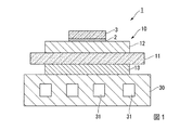
図1に、本実施形態に係るパワーモジュール用基板10を備えたパワーモジュール1を示す。
このパワーモジュール1は、回路層12が配設されたパワーモジュール用基板10と、回路層12の一方の面(図1において上面)に接合層2を介して接合された半導体素子3と、パワーモジュール用基板10の他方側(図1において下側)に配置されたヒートシンク30と、を備えている。
Embodiments of the present invention will be described below with reference to the accompanying drawings.
FIG. 1 shows a
The
パワーモジュール用基板10は、図2に示すように、セラミックス基板11と、このセラミックス基板11の一方の面(図2において上面)に配設された回路層12と、セラミックス基板11の他方の面(図2において下面)に配設された金属層13と、を備えている。
As shown in FIG. 2, the
セラミックス基板11は、絶縁性の高いAlN(窒化アルミ)、Si3N4(窒化ケイ素)、Al2O3(アルミナ)等のセラミックスで構成されている。本実施形態では、放熱性の優れたAlN(窒化アルミ)で構成されている。また、セラミックス基板11の厚さは、0.2〜1.5mmの範囲内に設定されており、本実施形態では、0.635mmに設定されている。
The
回路層12は、セラミックス基板11の一方の面に、導電性を有する銅又は銅合金の金属板が接合されることにより形成されている。本実施形態においては、回路層12は、純度99.99質量%以上の銅の圧延板を接合することで形成されている。なお、回路層12の厚さは0.1mm以上1.0mm以下の範囲内に設定されており、本実施形態では、0.3mmに設定されている。
The
金属層13は、セラミックス基板11の他方の面に、アルミニウム又はアルミニウム合金の金属板が接合されることにより形成されている。本実施形態においては、金属層13は、純度99.99質量%以上のアルミニウムの圧延板を接合することで形成されている。なお、金属層13の厚さは0.1mm以上3.0mm以下の範囲内に設定されており、本実施形態では、1.6mmに設定されている。
The
半導体素子3は、Si等の半導体材料で構成されている。この半導体素子3と回路層12は、接合層2を介して接合されている。
接合層2は、例えばSn−Ag系、Sn−In系、若しくはSn−Ag−Cu系のはんだ材とされている。
The
The bonding layer 2 is made of, for example, a Sn—Ag, Sn—In, or Sn—Ag—Cu solder material.
ヒートシンク30は、前述のパワーモジュール用基板10からの熱を放散するためのものである。本実施形態においては、ヒートシンク30は、アルミニウム又はアルミニウム合金で構成されており、本実施形態ではA6063(アルミニウム合金)で構成されている。このヒートシンク30には、冷却用の流体が流れるための流路31が設けられている。なお、このヒートシンク30と金属層13とが、Al−Si系ろう材によって接合されている。
The
次に、本実施形態に係るパワーモジュール1の製造方法について、図3のフロー図及び図4を参照して説明する。
まず、図4に示すように、セラミックス基板11の一方の面(図4において上面)に、溶加材25、活性金属材26、及び回路層12となる銅板22を順に積層する(第一積層工程S01)とともに、セラミックス基板11の他方の面(図4において下面)に、図4に示すように、接合材27及び金属層13となるアルミニウム板23を順に積層する(第二積層工程S02)。すなわち、セラミックス基板11と銅板22の間において、セラミックス基板11側に溶加材25を配置し、銅板22側に活性金属材26を配置しており、セラミックス基板11とアルミニウム板23の間において、接合材27を配置している。
Next, a method for manufacturing the
First, as shown in FIG. 4, the
ここで、溶加材25は、融点が660℃以下のCu−P−Sn−Ni系ろう材、Cu−Sn系ろう材、又はCu−Al系ろう材、Cu−P−Sn−Ni系はんだ材又はCu−Sn系はんだ材とされている。また、望ましくは、融点が600℃以下とされているとよい。本実施形態では、溶加材25としてCu−P−Sn−Ni系ろう材箔(Cu−7mass%P−15mass%Sn−10mass%Ni)を用いている。溶加材25の厚みは、5μm以上150μm以下の範囲とされている。
Here, the
活性金属材26は、例えばTi、Zr、Nb、Hfといった活性元素のいずれか1種又は2種以上を含有するものとされており、本実施形態では、活性金属材26としてTi箔を用いている。活性金属材26の厚みは、1μm以上20μm以下の範囲とされている。
接合材27は、本実施形態では、融点降下元素であるSiを含有したAl−Si系ろう材とされており、具体的には、Al−7.5mass%Siろう材を用いている。
The
In the present embodiment, the
次に、セラミックス基板11、溶加材25、活性金属材26、銅板22、接合材27、及びアルミニウム板23を積層方向に加圧(圧力1〜35kgf/cm2)した状態で、真空加熱炉内に装入して加熱する(加熱処理工程S03)。ここで、本実施形態では、真空加熱炉内の圧力は10−6Pa以上10−3Pa以下の範囲内に、加熱温度は600℃以上650℃以下の範囲内に、加熱時間は30分以上360分以下の範囲に設定している。
Next, in a state where the
この加熱処理工程S03においては、活性金属材26(Ti箔)と銅板22とが固相拡散接合によって接合されるとともに、溶加材25が溶融して液相を形成し、この液相が凝固することにより、溶加材25を介して、セラミックス基板11と活性金属材26とが接合されることになる。また、加熱処理工程S03においては、接合材27が溶融して液相を形成し、この液相が凝固することにより、接合材27を介してセラミックス基板11とアルミニウム板23とが接合される。
なお、固相拡散接合によって接合される活性金属材26と銅板22との接合面は、予め平滑な面とされている。
これにより、セラミックス基板11の一方の面に回路層12が形成されるとともに、セラミックス基板11の他方の面に金属層13が形成され、本実施形態であるパワーモジュール用基板10が製造される。
In this heat treatment step S03, the active metal material 26 (Ti foil) and the
In addition, the joining surface of the
As a result, the
次いで、パワーモジュール用基板10の金属層13の下面に、Al−Si系ろう材を介してヒートシンク30を接合する(ヒートシンク接合工程S04)。
次に、パワーモジュール用基板10の回路層12の上面に、はんだ材を介して半導体素子3を接合する(半導体素子接合工程S05)。
このようにして、本実施形態に係るパワーモジュール1が製造される。
Next, the
Next, the
In this way, the
以上のような構成とされた本実施形態のパワーモジュール用基板の製造方法によれば、セラミックス基板11と銅板22との間において、セラミックス基板11側に融点が660℃以下の溶加材25を配置し、銅板22側に活性金属材26(本実施形態においてはTi箔)を配置した状態で加熱処理を行う構成とされているので、加熱時に溶加材25が溶融した液相にTiが溶け込み、溶加材25の液相とセラミックス基板11との濡れ性が良好となる。したがって、溶加材25の液相が凝固した際に、溶加材25とセラミックス基板11との接合信頼性が向上する。
According to the method for manufacturing the power module substrate of the present embodiment configured as described above, the
また、本実施形態においては、活性金属材26と銅板22とを積層し、加圧した状態で、温度600℃以上650℃以下に加熱し保持する構成とされているので、活性金属材26に含まれるTi原子を銅板22中に拡散させ、銅板22に含まれる銅原子を活性金属材26中に拡散させ、活性金属材26と銅板22とを固相拡散接合することができる。
Further, in the present embodiment, the
加熱温度が600℃以上の場合、活性金属材26に含まれるTi原子と銅板22に含まれる銅原子との拡散が促進され、短時間で十分に固相拡散させることができる。また、加熱温度が650℃以下の場合、活性金属材26と銅板22との間に液相が生じて接合界面にコブが生じたり、厚みが変動したりすることを抑制できる。そのため、加熱温度は、上記の範囲に設定されている。
When the heating temperature is 600 ° C. or higher, diffusion of Ti atoms contained in the
また、加熱処理工程S03において、積層方向に加圧される圧力が1kgf/cm2以上の場合は、活性金属材26と銅板22とを十分に接合させることができ、活性金属材26と銅板22との間に隙間が生じることを抑制できる。また、加圧される圧力が35kgf/cm2以下の場合は、セラミックス基板11に割れが発生することを抑制できる。そのため、加圧される圧力は上記の範囲に設定されている。
In addition, in the heat treatment step S03, when the pressure applied in the stacking direction is 1 kgf / cm 2 or more, the
また、溶加材25の融点が660℃以下とされているので、Ag−Cu−Ti系ろう材を用いた場合と比較して、低温で溶加材の液相を形成することができる。
また、溶加材25と銅板22との間に活性金属材26が介在されているので、溶加材25の液相と銅板22とが直接接触することがなく、接合界面にコブが生じたり、厚みが変動したりすることを抑制できる。
さらに、活性金属材26と銅板22との接合される面は、予め平滑な面とされているので、接合界面に隙間が生じることを抑制でき、活性金属材26と銅板22とを確実に接合することができる。
Moreover, since melting | fusing point of the
Further, since the
Furthermore, since the surface where the
上述のように、溶加材25がセラミックス基板11と良好に接合されるとともに、活性金属材26と銅板22とが固相拡散接合によって接合されるので、セラミックス基板11と銅板22とを良好に接合でき、セラミックス基板11と回路層12との接合信頼性を向上させることができる。
さらに、Agを含有しない溶加材25を用いてセラミックス基板11と銅板22とを接合するので、Ag−Cu−Ti系ろう材を用いた場合よりも製造コストを低減できる。
As described above, since the
Furthermore, since the
さらに、上述したようにセラミックス基板11の一方の面に銅板22を低温で接合することができるので、セラミックス基板11の一方の面に銅板22を、他方の面にアルミニウム板23を同時に接合することができる。
Furthermore, since the
このように、セラミックス基板11の一方の面及び他方の面に、銅板22及びアルミニウム板23を同時に接合することで、製造工程を簡略化するとともに製造に要する時間を短縮し、製造コストを低減できる。さらに、一回の加熱処理で銅板22とアルミニウム板23を接合できるので、銅板22とアルミニウム板23を別々に接合する場合と比較して、セラミックス基板11にかかる熱負荷を低減でき、セラミックス基板11の反りを小さくしたり、セラミックス基板11の割れの発生を抑制したりすることが可能となる。
Thus, by simultaneously bonding the
また、本実施形態に係るパワーモジュール用基板10、パワーモジュール1によれば、セラミックス基板11の一方の面に銅板22からなる回路層12が形成されているので、半導体素子3からの熱を拡げてセラミックス基板11側に放散することができる。また、銅板22は変形抵抗が大きいので、ヒートサイクルが負荷された際に、回路層12の変形が抑制され、半導体素子3と回路層12とを接合する接合層2の変形を抑制し、接合信頼性を向上できる。
また、セラミックス基板11の他方の面にアルミニウム板23からなる金属層13が形成されているので、ヒートサイクル負荷時にパワーモジュール用基板10とヒートシンク30との間に生じる熱応力を金属層13によって吸収し、セラミックス基板11に割れが発生することを抑制できる。
Further, according to the
Further, since the
以上、本発明の実施形態について説明したが、本発明はこれに限定されることはなく、その発明の技術的思想を逸脱しない範囲で適宜変更可能である。 As mentioned above, although embodiment of this invention was described, this invention is not limited to this, It can change suitably in the range which does not deviate from the technical idea of the invention.
なお、上記実施の形態では、接合材としてAl−Si系ろう材を介してセラミックス基板とアルミニウム板を接合する場合について説明したが、これに限定されるものではなく、例えば、過渡液相接合法(Transient Liquid Phase Bonding、TLP)を適用して接合しても良い。過渡液相接合法では、図5に示すように、アルミニウム板23のうちセラミックス基板11との接合面に、スパッタリング法などによってSi、Cu等の添加元素を固着して固着層127を形成した後に、セラミックス基板11とアルミニウム板23を積層し、積層方向に加圧し、加熱処理を行うことでセラミックス基板11とアルミニウム板23を接合することができる。すなわち、過渡液相接合法では、接合材として固着層127を介してセラミックス基板11とアルミニウム板23
を積層し、銅板22とアルミニウム板23とを同時に接合することができる。
過渡液相接合法において、積層方向に加圧する際の圧力は、1kgf/cm2以上35kgf/cm2以下とされている。また、加熱処理における加熱温度及び加熱時間は、600℃以上650℃以下、30分以上360分以下とされている。
なお、固着層の添加元素として、Si、Cuの他に、Zn、Ge、Ag、Mg、Ca、Ga、又はLi等の添加元素を用いても良い。
In the above embodiment, the case where the ceramic substrate and the aluminum plate are bonded via the Al—Si brazing material as the bonding material has been described. However, the present invention is not limited to this. For example, the transient liquid phase bonding method (Transient Liquid Phase Bonding, TLP) may be applied for bonding. In the transient liquid phase bonding method, as shown in FIG. 5, after the fixed
The
In transient liquid phase bonding method, pressure applied in the lamination direction is a 1 kgf / cm 2 or more 35 kgf / cm 2 or less. Moreover, the heating temperature and the heating time in the heat treatment are 600 ° C. or more and 650 ° C. or less, and 30 minutes or more and 360 minutes or less.
In addition to Si and Cu, additive elements such as Zn, Ge, Ag, Mg, Ca, Ga, or Li may be used as the additive element of the fixed layer.
また、接合材として金属粒子と有機物とを有する金属ペーストを用いることでセラミックス基板とアルミニウム板を接合することもできる。金属ペーストとしては、例えばAg粒子と有機物とを有するAgペーストが挙げられる。具体的には、図6に示すように、セラミックス基板11の他方の面に、スクリーン印刷などによってAgペースト227を塗布し、Agペースト227を介してセラミックス基板11とアルミニウム板23を積層し加熱処理を行うことで、銅板22とアルミニウム板23をセラミックス基板11に同時に接合できる。Agペースト227を用いて接合する場合、積層方向に加圧する際の圧力は、1kgf/cm2以上35kgf/cm2以下とされている。また、加熱処理における加熱温度及び加熱時間は、600℃以上650℃以下、30分以上360分以下とされている。
In addition, the ceramic substrate and the aluminum plate can be bonded by using a metal paste having metal particles and an organic substance as a bonding material. Examples of the metal paste include an Ag paste having Ag particles and an organic substance. Specifically, as shown in FIG. 6, an
また、上記の実施形態では、パワーモジュール用基板とヒートシンクとをAl−Si系ろう材を介して接合する場合について説明したが、これに限定されるものではなく、例えば上述した過渡液相接合法(TLP)を適用し、固着層を介してパワーモジュール用基板とヒートシンクとを接合しても良い。また、Ag粒子と有機物とを有するAgペーストを介してパワーモジュール用基板とヒートシンクとを接合しても良い。
さらに、ヒートシンクとして冷却用の流路を有するもので説明したが、ヒートシンクの構造に特に限定はなく、例えば空冷方式のヒートシンクであってもよい。また、ヒートシンクは、放熱フィンを有していても良い。
Further, in the above embodiment, the case where the power module substrate and the heat sink are bonded via the Al—Si brazing material has been described. However, the present invention is not limited to this, for example, the transient liquid phase bonding method described above. (TLP) may be applied, and the power module substrate and the heat sink may be bonded to each other through the fixing layer. Further, the power module substrate and the heat sink may be joined via an Ag paste containing Ag particles and an organic substance.
Furthermore, although it has been described that the heat sink has a cooling channel, the structure of the heat sink is not particularly limited, and for example, an air-cooled heat sink may be used. Moreover, the heat sink may have a radiation fin.
以下に、本発明の効果を確認すべく行った確認実験の結果について説明する。
まず、AlNからなるセラミックス基板(40mm×40mm×0.635mmt)の一方の面に表1に示す溶加材、活性金属材、純度99.99%の銅からなる銅板(37mm×37mm×0.3mmt)を積層し、他方の面に表1に示す接合材を介してアルミニウム板(37mm×37mm×1.6mmt)を積層する。
なお、活性金属の位置が銅板側とされた本発明例1〜12については、セラミックス基板/溶加材/活性金属材/銅板の順に積層し、セラミックス基板側とされた本発明例13についてはセラミックス基板/活性金属材/溶加材/銅板の順に積層した。
なお、表1に示す接合材として、「Al−Si」は、Al−7.5mass%Siろう材とした。「Cu(TLP)」は、固着層としてCuを用いた。「Agペースト」は、Ag粒子と有機物とを含むAgペーストとした。
Below, the result of the confirmation experiment performed in order to confirm the effect of this invention is demonstrated.
First, on one surface of a ceramic substrate made of AlN (40 mm × 40 mm × 0.635 mmt), a filler material shown in Table 1, an active metal material, and a copper plate made of copper with a purity of 99.99% (37 mm × 37 mm × 0.00 mm). 3 mmt) is laminated, and an aluminum plate (37 mm × 37 mm × 1.6 mmt) is laminated on the other surface via the bonding material shown in Table 1.
As for Invention Examples 1 to 12, where the position of the active metal was on the copper plate side, the ceramic substrate / filler material / active metal material / copper plate was laminated in this order, and Example 13 of the invention was set to the ceramic substrate side. The layers were laminated in the order of ceramic substrate / active metal material / filler material / copper plate.
In addition, as a bonding material shown in Table 1, “Al—Si” was an Al-7.5 mass% Si brazing material. “Cu (TLP)” used Cu as the fixing layer. The “Ag paste” was an Ag paste containing Ag particles and organic matter.
そして、積層方向に圧力12kgf/cm2で加圧した状態で真空加熱炉内に装入し、加熱することによってセラミックス基板の一方の面に銅板を接合し、他方の面にアルミニウム板を接合し、セラミックス基板の一方の面及び他方の面に回路層及び金属層を形成した。ここで、真空加熱炉内の圧力を10−6Pa以上、10−3Pa以下の範囲内に設定し、加熱温度及び加熱時間は表1に示す条件とした。このようにしてパワーモジュール用基板を得た。 Then, in a state where the pressure is 12 kgf / cm 2 in the lamination direction, the copper plate is bonded to one surface of the ceramic substrate and heated to bond the aluminum plate to the other surface. A circuit layer and a metal layer were formed on one surface and the other surface of the ceramic substrate. Here, the pressure in the vacuum heating furnace was set in the range of 10 −6 Pa to 10 −3 Pa, and the heating temperature and the heating time were set as shown in Table 1. In this way, a power module substrate was obtained.
次いで、上述のパワーモジュール用基板の金属層の他方の面側にヒートシンクを接合した。ヒートシンクは、A6063からなるアルミニウム板(50mm×60mm×5mmt)とし、ヒートシンクの接合は表1に示す方法で行った。表1のヒートシンクの接合方法に示す「Al−Si」では、Al−10.5mass%Siろう材を用い、「Cu(TLP)」では、Cuの固着層を用い、「Agペースト」では、Ag粒子と有機物とを含むAgペーストを用いて接合を行った。パワーモジュール用基板とセラミックス基板の接合時の圧力は12kgf/cm2、加熱温度は610℃、加熱時間は60分とし、真空雰囲気で行った。
このようにして、本発明例1〜13のヒートシンク付パワーモジュール用基板を作製した。
Next, a heat sink was bonded to the other surface side of the metal layer of the power module substrate described above. The heat sink was an aluminum plate (50 mm × 60 mm × 5 mmt) made of A6063, and the heat sink was joined by the method shown in Table 1. In “Al-Si” shown in Table 1 for the heat sink bonding method, Al-10.5 mass% Si brazing material is used, in “Cu (TLP)”, a fixed layer of Cu is used, and in “Ag paste”, Ag is used. Bonding was performed using an Ag paste containing particles and organic matter. The pressure at the time of joining the power module substrate and the ceramic substrate was 12 kgf / cm 2 , the heating temperature was 610 ° C., the heating time was 60 minutes, and it was performed in a vacuum atmosphere.
In this way, power module substrates with heat sinks of Invention Examples 1 to 13 were produced.
上述のようにして得られた本発明例のヒートシンク付パワーモジュール用基板に対して、回路層とセラミックス基板との接合率、及び金属層とセラミックス基板との接合率を評価した。さらに、ヒートシンク付パワーモジュール用基板に対して、冷熱サイクル試験を行い、試験後の回路層とセラミックス基板との接合率、及び金属層とセラミックス基板との接合率を評価した。
冷熱サイクルの試験方法と、接合率の評価方法を以下に説明する。
With respect to the power module substrate with a heat sink of the present invention obtained as described above, the bonding rate between the circuit layer and the ceramic substrate and the bonding rate between the metal layer and the ceramic substrate were evaluated. Furthermore, a thermal cycle test was performed on the power module substrate with a heat sink, and the bonding rate between the circuit layer and the ceramic substrate after the test and the bonding rate between the metal layer and the ceramic substrate were evaluated.
A test method for the cooling / heating cycle and a method for evaluating the bonding rate will be described below.
(冷熱サイクル試験)
冷熱サイクル試験は、冷熱衝撃試験機エスペック社製TSB−51を使用し、ヒートシンク付パワーモジュール用基板に対して、液相(フロリナート)で、−40℃×5分←→125℃×5分の3000サイクルを実施した。
(Cooling cycle test)
The thermal cycle test uses TSB-51 manufactured by ESPEC, a thermal shock tester, and is in a liquid phase (Fluorinert) with respect to a power module substrate with a heat sink at −40 ° C. × 5 minutes ← → 125 ° C. × 5 minutes 3000 cycles were performed.
(接合率評価)
ヒートシンク付パワーモジュール用基板に対し、セラミックス基板と回路層との界面の接合率、及びセラミックス基板と金属層との界面の接合率について超音波探傷装置を用いて評価し、以下の式から算出した。
ここで、初期接合面積とは、接合前における接合すべき面積、すなわち本実施例では回路層及び金属層の面積とした。超音波探傷像において剥離は接合部内の白色部で示されることから、この白色部の面積を剥離面積とした。なお、セラミックス基板、回路層、及び金属層にクラックが生じた場合、このクラックは超音波探傷像において白色部で示され、クラックも剥離面積として評価されることになる。
(接合率(%))={(初期接合面積)−(剥離面積)}/(初期接合面積)×100
以上の評価の結果を表1に示す。
(Joint rate evaluation)
For the power module substrate with a heat sink, the bonding rate at the interface between the ceramic substrate and the circuit layer and the bonding rate at the interface between the ceramic substrate and the metal layer were evaluated using an ultrasonic flaw detector, and calculated from the following equations: .
Here, the initial bonding area is the area to be bonded before bonding, that is, the area of the circuit layer and the metal layer in this embodiment. In the ultrasonic flaw detection image, peeling is indicated by a white portion in the joint, and thus the area of the white portion was taken as the peeling area. In addition, when a crack arises in a ceramic substrate, a circuit layer, and a metal layer, this crack is shown by a white part in an ultrasonic flaw detection image, and a crack will be evaluated as a peeling area.
(Bonding rate (%)) = {(initial bonding area) − (peeling area)} / (initial bonding area) × 100
The results of the above evaluation are shown in Table 1.

融点が660℃以下の溶加材を用い、セラミックス基板の一方の面及び他方の面に回路層及び金属層を同時に形成した本発明例1〜13においては、初期の接合率は高く、冷熱サイクルが負荷された後も高い接合率を維持できるヒートシンク付パワーモジュール用基板が得られることが確認された。 In Examples 1 to 13 of the present invention in which a circuit layer and a metal layer were simultaneously formed on one surface and the other surface of a ceramic substrate using a filler material having a melting point of 660 ° C. or less, the initial joining rate was high, and the thermal cycle It was confirmed that a power module substrate with a heat sink capable of maintaining a high bonding rate even after being loaded was obtained.
10 パワーモジュール用基板
11 セラミックス基板
12 回路層
13 金属層
22 銅板
23 アルミニウム板
25 溶加材
26 活性金属材
27、127、227 接合材
DESCRIPTION OF
Claims (7)
前記セラミックス基板の一方の面側において、活性金属材及び融点が660℃以下の溶加材を介して、前記セラミックス基板と前記銅板とを積層する第一積層工程と、
前記セラミックス基板の他方の面側において、接合材を介して前記セラミックス基板と前記アルミニウム板とを積層する第二積層工程と、
積層された前記セラミックス基板、前記銅板、及び前記アルミニウム板を加熱処理する加熱処理工程と、を備え、
前記セラミックス基板と前記銅板、及び前記セラミックス基板と前記アルミニウム板を同時に接合することを特徴とするパワーモジュール用基板の製造方法。 Production of a substrate for a power module comprising a ceramic substrate, a circuit layer formed by bonding a copper plate to one surface of the ceramic substrate, and a metal layer formed by bonding an aluminum plate to the other surface of the ceramic substrate A method,
A first laminating step of laminating the ceramic substrate and the copper plate via an active metal material and a filler material having a melting point of 660 ° C. or less on one surface side of the ceramic substrate;
A second laminating step of laminating the ceramic substrate and the aluminum plate via a bonding material on the other surface side of the ceramic substrate;
A heat treatment step of heat-treating the laminated ceramic substrate, the copper plate, and the aluminum plate,
A method of manufacturing a power module substrate, wherein the ceramic substrate and the copper plate, and the ceramic substrate and the aluminum plate are bonded simultaneously.
Priority Applications (7)
| Application Number | Priority Date | Filing Date | Title |
|---|---|---|---|
| JP2013055518A JP6111764B2 (en) | 2013-03-18 | 2013-03-18 | Power module substrate manufacturing method |
| PCT/JP2014/057098 WO2014148420A1 (en) | 2013-03-18 | 2014-03-17 | Method for manufacturing power-module substrate |
| CN201480012586.1A CN105027277B (en) | 2013-03-18 | 2014-03-17 | The manufacture method of power module substrate |
| KR1020157025159A KR102224535B1 (en) | 2013-03-18 | 2014-03-17 | Method for manufacturing power-module substrate |
| US14/772,913 US9833855B2 (en) | 2013-03-18 | 2014-03-17 | Method for manufacturing power module substrate |
| EP14767678.7A EP2978018B1 (en) | 2013-03-18 | 2014-03-17 | Method for manufacturing power-module substrate |
| TW103110093A TWI614845B (en) | 2013-03-18 | 2014-03-18 | Method of producing substrate for power module |
Applications Claiming Priority (1)
| Application Number | Priority Date | Filing Date | Title |
|---|---|---|---|
| JP2013055518A JP6111764B2 (en) | 2013-03-18 | 2013-03-18 | Power module substrate manufacturing method |
Publications (2)
| Publication Number | Publication Date |
|---|---|
| JP2014183119A JP2014183119A (en) | 2014-09-29 |
| JP6111764B2 true JP6111764B2 (en) | 2017-04-12 |
Family
ID=51580099
Family Applications (1)
| Application Number | Title | Priority Date | Filing Date |
|---|---|---|---|
| JP2013055518A Active JP6111764B2 (en) | 2013-03-18 | 2013-03-18 | Power module substrate manufacturing method |
Country Status (7)
| Country | Link |
|---|---|
| US (1) | US9833855B2 (en) |
| EP (1) | EP2978018B1 (en) |
| JP (1) | JP6111764B2 (en) |
| KR (1) | KR102224535B1 (en) |
| CN (1) | CN105027277B (en) |
| TW (1) | TWI614845B (en) |
| WO (1) | WO2014148420A1 (en) |
Families Citing this family (22)
| Publication number | Priority date | Publication date | Assignee | Title |
|---|---|---|---|---|
| JP5672324B2 (en) * | 2013-03-18 | 2015-02-18 | 三菱マテリアル株式会社 | Manufacturing method of joined body and manufacturing method of power module substrate |
| EP3041045B1 (en) * | 2013-08-26 | 2019-09-18 | Mitsubishi Materials Corporation | Bonded body and power module substrate |
| JP6127833B2 (en) * | 2013-08-26 | 2017-05-17 | 三菱マテリアル株式会社 | Manufacturing method of joined body and manufacturing method of power module substrate |
| JP6079505B2 (en) | 2013-08-26 | 2017-02-15 | 三菱マテリアル株式会社 | Bonded body and power module substrate |
| JP5720839B2 (en) * | 2013-08-26 | 2015-05-20 | 三菱マテリアル株式会社 | Bonded body and power module substrate |
| US9969654B2 (en) * | 2014-01-24 | 2018-05-15 | United Technologies Corporation | Method of bonding a metallic component to a non-metallic component using a compliant material |
| TWI619207B (en) * | 2014-03-20 | 2018-03-21 | 三菱綜合材料股份有限公司 | Bonded body, power module substrate, power module and method of producing bonded body |
| JP6256176B2 (en) * | 2014-04-25 | 2018-01-10 | 三菱マテリアル株式会社 | Manufacturing method of joined body, manufacturing method of power module substrate |
| JP6471465B2 (en) * | 2014-11-11 | 2019-02-20 | 三菱マテリアル株式会社 | Power module board with cooler |
| JP2016184602A (en) * | 2015-03-25 | 2016-10-20 | 京セラ株式会社 | Circuit board |
| JP6638282B2 (en) * | 2015-09-25 | 2020-01-29 | 三菱マテリアル株式会社 | Light emitting module with cooler and method of manufacturing light emitting module with cooler |
| DE102015224464A1 (en) * | 2015-12-07 | 2017-06-08 | Aurubis Stolberg Gmbh & Co. Kg | Copper-ceramic substrate, copper semi-finished product for producing a copper-ceramic substrate and method for producing a copper-ceramic substrate |
| CN106328543A (en) * | 2016-08-24 | 2017-01-11 | 浙江德汇电子陶瓷有限公司 | Manufacturing method of metal-ceramic composite substrate and composite substrate manufactured by manufacturing method |
| JP7052374B2 (en) | 2017-02-06 | 2022-04-12 | 三菱マテリアル株式会社 | Manufacturing method of ceramics / aluminum joint, manufacturing method of insulated circuit board |
| JP6965768B2 (en) * | 2017-02-28 | 2021-11-10 | 三菱マテリアル株式会社 | Copper / Ceramics Joint, Insulated Circuit Board, Copper / Ceramics Joint Manufacturing Method, Insulated Circuit Board Manufacturing Method |
| DE102017205813A1 (en) * | 2017-04-05 | 2018-10-11 | Mahle International Gmbh | A method of manufacturing a cooling device, a cooling device and a cooling arrangement |
| JP7124633B2 (en) * | 2017-10-27 | 2022-08-24 | 三菱マテリアル株式会社 | Joined body and insulating circuit board |
| JP7230432B2 (en) * | 2017-11-02 | 2023-03-01 | 三菱マテリアル株式会社 | Joined body and insulating circuit board |
| JP7192451B2 (en) * | 2018-01-25 | 2022-12-20 | 三菱マテリアル株式会社 | COPPER/CERAMIC JOINT, INSULATED CIRCUIT BOARD, METHOD FOR MANUFACTURING COPPER/CERAMIC JOINT, AND METHOD FOR MANUFACTURING INSULATED CIRCUIT BOARD |
| CN114303237A (en) * | 2019-08-29 | 2022-04-08 | 京瓷株式会社 | Circuit board and power module |
| JP7460656B2 (en) * | 2019-11-27 | 2024-04-02 | 日本碍子株式会社 | Manufacturing method of bonded substrate |
| TWI795199B (en) * | 2022-01-28 | 2023-03-01 | 奇鋐科技股份有限公司 | Manufacturing method of thermal module |
Family Cites Families (45)
| Publication number | Priority date | Publication date | Assignee | Title |
|---|---|---|---|---|
| US5561321A (en) * | 1992-07-03 | 1996-10-01 | Noritake Co., Ltd. | Ceramic-metal composite structure and process of producing same |
| JP3211856B2 (en) | 1994-11-02 | 2001-09-25 | 電気化学工業株式会社 | Circuit board |
| JP4077888B2 (en) * | 1995-07-21 | 2008-04-23 | 株式会社東芝 | Ceramic circuit board |
| JP3933287B2 (en) * | 1998-01-30 | 2007-06-20 | 電気化学工業株式会社 | Circuit board with heat sink |
| JP2001148451A (en) | 1999-03-24 | 2001-05-29 | Mitsubishi Materials Corp | Power module board |
| JP2000349400A (en) | 1999-06-04 | 2000-12-15 | Denki Kagaku Kogyo Kk | Circuit board |
| DE60107670T2 (en) * | 2001-02-27 | 2005-10-06 | Sumida Corp. | LEAD-FREE SOLDERING ALLOY AND THEIR USE IN ELECTRONIC COMPONENTS |
| JP2003197826A (en) * | 2001-12-26 | 2003-07-11 | Toshiba Corp | Ceramic circuit board and semiconductor module using the same |
| US9533379B2 (en) * | 2002-08-23 | 2017-01-03 | Lincoln Global, Inc. | Phosphorous-copper base brazing alloy |
| JP4206915B2 (en) * | 2002-12-27 | 2009-01-14 | 三菱マテリアル株式会社 | Power module substrate |
| JP4394477B2 (en) | 2003-03-27 | 2010-01-06 | Dowaホールディングス株式会社 | Method for producing metal / ceramic bonding substrate |
| BRPI0410277A (en) * | 2003-05-13 | 2006-05-16 | Reactive Nanotechnologies Inc | method for simulating a behavior of an energy distribution within an assembly containing a reactive multilayer material, machine readable program storage device, method for joining, and, joining |
| JP4362597B2 (en) * | 2003-05-30 | 2009-11-11 | Dowaメタルテック株式会社 | Metal-ceramic circuit board and manufacturing method thereof |
| JP2005050919A (en) * | 2003-07-30 | 2005-02-24 | Ngk Spark Plug Co Ltd | Circuit board and semiconductor device |
| JP2005052869A (en) * | 2003-08-06 | 2005-03-03 | Sumitomo Metal Mining Co Ltd | Brazing material for high temperature soldering and semiconductor device using it |
| JP4207896B2 (en) * | 2005-01-19 | 2009-01-14 | 富士電機デバイステクノロジー株式会社 | Semiconductor device |
| US7749430B2 (en) * | 2005-01-20 | 2010-07-06 | A.L.M.T. Corp. | Member for semiconductor device and production method thereof |
| DE102005032076B3 (en) * | 2005-07-08 | 2007-02-08 | Infineon Technologies Ag | Method for producing a circuit module |
| DE102005061049A1 (en) * | 2005-12-19 | 2007-06-21 | Curamik Electronics Gmbh | Metal-ceramic substrate |
| US8164176B2 (en) * | 2006-10-20 | 2012-04-24 | Infineon Technologies Ag | Semiconductor module arrangement |
| JP2008198706A (en) * | 2007-02-09 | 2008-08-28 | Hitachi Metals Ltd | Circuit board, method for manufacturing the same, and semiconductor module using the same |
| CN101687717A (en) * | 2007-04-24 | 2010-03-31 | 陶瓷技术股份公司 | Component having a metalized ceramic base |
| US7821130B2 (en) * | 2008-03-31 | 2010-10-26 | Infineon Technologies Ag | Module including a rough solder joint |
| WO2009148168A1 (en) * | 2008-06-06 | 2009-12-10 | 三菱マテリアル株式会社 | Substrate for power module, power module, and method for producing substrate for power module |
| US20100175756A1 (en) * | 2009-01-15 | 2010-07-15 | Weihs Timothy P | Method For Bonding Of Concentrating Photovoltaic Receiver Module To Heat Sink Using Foil And Solder |
| WO2010088504A1 (en) * | 2009-01-29 | 2010-08-05 | Smith International, Inc. | Brazing methods for pdc cutters |
| JP5504842B2 (en) * | 2009-11-20 | 2014-05-28 | 三菱マテリアル株式会社 | Power module substrate, power module substrate with heat sink, power module, and method for manufacturing power module substrate |
| JP5363361B2 (en) * | 2010-01-28 | 2013-12-11 | 本田技研工業株式会社 | Semiconductor device and manufacturing method thereof |
| JP5577980B2 (en) * | 2010-09-16 | 2014-08-27 | 三菱マテリアル株式会社 | Power module substrate with heat sink, power module, and method for manufacturing power module substrate with heat sink |
| JP2012136378A (en) | 2010-12-25 | 2012-07-19 | Kyocera Corp | Circuit board and electronic device using the same |
| JP5736807B2 (en) | 2011-02-02 | 2015-06-17 | 三菱マテリアル株式会社 | Power module substrate with heat sink, manufacturing method of power module substrate with heat sink, and power module |
| JP2012178513A (en) * | 2011-02-28 | 2012-09-13 | Mitsubishi Materials Corp | Power module unit and manufacturing method of the same |
| US20130022836A1 (en) * | 2011-07-20 | 2013-01-24 | Diamond Innovations, Inc. | Brazed coated diamond-containing materials |
| DE112012003228B4 (en) * | 2011-08-04 | 2021-08-12 | Mitsubishi Electric Corporation | Semiconductor device and method of manufacturing the same |
| CN104067386B (en) * | 2012-02-01 | 2019-05-28 | 三菱综合材料株式会社 | The manufacturing method of power module substrate |
| JP5910166B2 (en) | 2012-02-29 | 2016-04-27 | 三菱マテリアル株式会社 | Power module substrate manufacturing method |
| JP2013229579A (en) * | 2012-03-30 | 2013-11-07 | Mitsubishi Materials Corp | Substrate for power module, substrate for power module having heat sink, and power module |
| JP6044097B2 (en) * | 2012-03-30 | 2016-12-14 | 三菱マテリアル株式会社 | Power module substrate with heat sink, power module substrate with cooler, and power module |
| WO2014061588A1 (en) * | 2012-10-16 | 2014-04-24 | 三菱マテリアル株式会社 | Substrate for power module with heat sink, power module with heat sink, and method for producing substrate for power module with heat sink |
| CN102922828B (en) | 2012-10-24 | 2015-04-22 | 浙江工贸职业技术学院 | Composite board of copper-foil-bonded ceramic substrate and preparation method of composite board |
| JP6056432B2 (en) * | 2012-12-06 | 2017-01-11 | 三菱マテリアル株式会社 | Power module substrate, power module substrate with heat sink, power module, power module substrate manufacturing method |
| JP5664679B2 (en) * | 2013-03-07 | 2015-02-04 | 三菱マテリアル株式会社 | Power module substrate manufacturing method |
| KR102130868B1 (en) * | 2013-03-14 | 2020-07-08 | 미쓰비시 마테리알 가부시키가이샤 | Bonded body, substrate for power modules, and substrate with heat sink for power modules |
| JP5672324B2 (en) * | 2013-03-18 | 2015-02-18 | 三菱マテリアル株式会社 | Manufacturing method of joined body and manufacturing method of power module substrate |
| JP3211856U (en) | 2017-05-09 | 2017-08-10 | 株式会社アイエスピー | Towel with measure |
-
2013
- 2013-03-18 JP JP2013055518A patent/JP6111764B2/en active Active
-
2014
- 2014-03-17 EP EP14767678.7A patent/EP2978018B1/en not_active Not-in-force
- 2014-03-17 KR KR1020157025159A patent/KR102224535B1/en active IP Right Grant
- 2014-03-17 US US14/772,913 patent/US9833855B2/en active Active
- 2014-03-17 WO PCT/JP2014/057098 patent/WO2014148420A1/en active Application Filing
- 2014-03-17 CN CN201480012586.1A patent/CN105027277B/en not_active Expired - Fee Related
- 2014-03-18 TW TW103110093A patent/TWI614845B/en not_active IP Right Cessation
Also Published As
| Publication number | Publication date |
|---|---|
| CN105027277A (en) | 2015-11-04 |
| EP2978018A4 (en) | 2016-11-02 |
| CN105027277B (en) | 2018-04-20 |
| US20160016245A1 (en) | 2016-01-21 |
| TWI614845B (en) | 2018-02-11 |
| TW201508871A (en) | 2015-03-01 |
| JP2014183119A (en) | 2014-09-29 |
| WO2014148420A1 (en) | 2014-09-25 |
| EP2978018A1 (en) | 2016-01-27 |
| EP2978018B1 (en) | 2018-05-02 |
| KR20150133191A (en) | 2015-11-27 |
| KR102224535B1 (en) | 2021-03-05 |
| US9833855B2 (en) | 2017-12-05 |
Similar Documents
| Publication | Publication Date | Title |
|---|---|---|
| JP6111764B2 (en) | Power module substrate manufacturing method | |
| JP5672324B2 (en) | Manufacturing method of joined body and manufacturing method of power module substrate | |
| JP5403129B2 (en) | Power module substrate, power module substrate with heat sink, power module, and method for manufacturing power module substrate | |
| JP6079505B2 (en) | Bonded body and power module substrate | |
| JP6307832B2 (en) | Power module board, power module board with heat sink, power module with heat sink | |
| KR102097177B1 (en) | Power module substrate, power module substrate with heat sink, and power module | |
| KR102154889B1 (en) | Method for manufacturing assembly and method for manufacturing power-module substrate | |
| JP5720839B2 (en) | Bonded body and power module substrate | |
| TWI637466B (en) | Jointed body and power module substrate | |
| JP5904257B2 (en) | Power module substrate manufacturing method | |
| JP2014039062A (en) | Substrate for power module, substrate for power module having heat sink, power module, and method for manufacturing substrate for power module | |
| JP6303420B2 (en) | Power module substrate | |
| TWI708754B (en) | Bonded body, power module substrate, power mosule, method of producing bonded body and method of producing power module substrate | |
| JP6327058B2 (en) | Power module substrate with heat sink, method of manufacturing joined body, method of manufacturing power module substrate, and method of manufacturing power module substrate with heat sink | |
| KR20180104659A (en) | Junction body, substrate for power module, method of manufacturing junction body, and method of manufacturing substrate for power module | |
| JP6299442B2 (en) | Power module | |
| JP6885104B2 (en) | Manufacturing method of insulated circuit board | |
| JP2015070098A (en) | Substrate for power module with copper plate, and method of manufacturing substrate for power module with copper plate |
Legal Events
| Date | Code | Title | Description |
|---|---|---|---|
| A621 | Written request for application examination |
Free format text: JAPANESE INTERMEDIATE CODE: A621 Effective date: 20150930 |
|
| A131 | Notification of reasons for refusal |
Free format text: JAPANESE INTERMEDIATE CODE: A131 Effective date: 20160705 |
|
| TRDD | Decision of grant or rejection written | ||
| A01 | Written decision to grant a patent or to grant a registration (utility model) |
Free format text: JAPANESE INTERMEDIATE CODE: A01 Effective date: 20170214 |
|
| A61 | First payment of annual fees (during grant procedure) |
Free format text: JAPANESE INTERMEDIATE CODE: A61 Effective date: 20170227 |
|
| R150 | Certificate of patent or registration of utility model |
Ref document number: 6111764 Country of ref document: JP Free format text: JAPANESE INTERMEDIATE CODE: R150 |