JP2009076594A - Electronic circuit module - Google Patents
Electronic circuit module Download PDFInfo
- Publication number
- JP2009076594A JP2009076594A JP2007242759A JP2007242759A JP2009076594A JP 2009076594 A JP2009076594 A JP 2009076594A JP 2007242759 A JP2007242759 A JP 2007242759A JP 2007242759 A JP2007242759 A JP 2007242759A JP 2009076594 A JP2009076594 A JP 2009076594A
- Authority
- JP
- Japan
- Prior art keywords
- frame
- electronic circuit
- circuit module
- lower cover
- cover
- Prior art date
- Legal status (The legal status is an assumption and is not a legal conclusion. Google has not performed a legal analysis and makes no representation as to the accuracy of the status listed.)
- Granted
Links
Images


Classifications
-
- H—ELECTRICITY
- H05—ELECTRIC TECHNIQUES NOT OTHERWISE PROVIDED FOR
- H05K—PRINTED CIRCUITS; CASINGS OR CONSTRUCTIONAL DETAILS OF ELECTRIC APPARATUS; MANUFACTURE OF ASSEMBLAGES OF ELECTRICAL COMPONENTS
- H05K5/00—Casings, cabinets or drawers for electric apparatus
- H05K5/02—Details
- H05K5/03—Covers
-
- H—ELECTRICITY
- H05—ELECTRIC TECHNIQUES NOT OTHERWISE PROVIDED FOR
- H05K—PRINTED CIRCUITS; CASINGS OR CONSTRUCTIONAL DETAILS OF ELECTRIC APPARATUS; MANUFACTURE OF ASSEMBLAGES OF ELECTRICAL COMPONENTS
- H05K5/00—Casings, cabinets or drawers for electric apparatus
- H05K5/04—Metal casings
Abstract
Description
本発明は、高周波回路が設けられた回路基板を枠体の内部でカバーに覆われる空間に組み込んで電磁的にシールドされるようになしたチューナ等の電子回路モジュールに関する。 The present invention relates to an electronic circuit module such as a tuner that is electromagnetically shielded by incorporating a circuit board provided with a high-frequency circuit into a space covered by a cover inside a frame.
一般的に、この種の電子回路モジュールは、金属板からなる枠体やカバーを組み合わせて筐体が構成され、この筐体の内部空間に回路基板が設置されている。筐体の複数箇所には取付脚が下向きに突設されており、電子回路モジュールをマザーボード上に実装する際に、これら取付脚をマザーボードの接地用パターンに半田付けすることによって、筐体がシールドケースとして機能するようになっている。 In general, this type of electronic circuit module has a casing formed by combining a frame and a cover made of a metal plate, and a circuit board is installed in the internal space of the casing. Mounting legs are projected downward at multiple locations on the chassis. When mounting the electronic circuit module on the motherboard, the chassis is shielded by soldering these mounting legs to the grounding pattern on the motherboard. It comes to function as a case.
従来公知の電子回路モジュールにおいて、取付脚を筐体の底板部材である下カバーに設けているものもあるが、下カバーは比較的肉薄な金属板からなるため、組立時などに取付脚に変形が起こりやすいという問題があった。また、下カバーの取付脚がマザーボードに半田付けされていると、アンテナコネクタ着脱時などに作用する外力によって下カバーが外れやすくなるという問題もあった。 In some known electronic circuit modules, the mounting legs are provided on the lower cover, which is the bottom plate member of the housing. However, the lower cover is made of a relatively thin metal plate, so it is transformed into the mounting legs during assembly. There was a problem that was likely to occur. In addition, when the mounting leg of the lower cover is soldered to the motherboard, there is a problem that the lower cover is easily detached due to an external force acting when the antenna connector is attached or detached.
そこで従来より、筐体の側板部材である枠体に取付脚を設けることによって、上記の問題点を解決した電子回路モジュールが提案されている(例えば、特許文献1参照)。すなわち、枠体は方形枠状に配設されて回路基板を囲繞する側板によって主に構成されており、回路基板が取り付けられる枠体の側板は下カバーよりも肉厚で機械的強度に富む金属板によって形成されているので、枠体の側板に設けられた取付脚は組立時などに不所望な変形を生じにくい。また、枠体の一部である取付脚がマザーボードに半田付けされていれば、アンテナコネクタ着脱時などに作用する外力に対しても強くなるため信頼性が高まる。
しかしながら、特許文献1に開示された従来の電子回路モジュールでは、枠体(側板)の下縁から下向きにまっすぐ取付脚が突設されているため、枠体の下端部に下カバーを嵌着させるうえで必要な下カバーの弾性片を、取付脚との干渉を避けた位置に形成しなければならないという制約があり、その影響で枠体に対する下カバーの嵌合強度が不足しやすいという難点がある。つまり、下カバーの周縁部には複数箇所に弾性片が上向きに突設されており、これら弾性片を撓ませながら枠体の下端部に外嵌させることによって下カバーが枠体に取り付けられるため、下カバーの周縁部で枠体の取付脚と対向する部分に弾性片を設けると、この弾性片が組立時に取付脚と干渉して不所望な変形を起こしやすくなる。このような理由から下カバーの周縁部で枠体の取付脚と対向する部分に取付脚用の逃げ部が必要となり、かかる逃げ部によって下カバーの嵌合強度が低下することとなる。また、下カバーの逃げ部の近傍に設けられた弾性片は強い弾発力を生起することができないため、この点でも下カバーの嵌合強度は不足しやすかった。なお、枠体に対する下カバーの嵌合強度が不足しているとラットルノイズが発生しやすくなり、該下カバーが枠体から外れる危険性も高まる。
However, in the conventional electronic circuit module disclosed in
また、前述した従来の電子回路モジュールの場合、枠体の取付脚が挿通される取付孔をマザーボードの周縁部に穿設することは好ましくないため、マザーボード上における電子回路モジュールの実装領域を周縁部からある程度内側へ離隔させておかねばならず、それゆえ実装位置が制約されるという問題もあった。 In addition, in the case of the above-described conventional electronic circuit module, it is not preferable to make a mounting hole through which the mounting leg of the frame body is inserted in the peripheral portion of the motherboard, so that the mounting region of the electronic circuit module on the motherboard is the peripheral portion. There is also a problem that the mounting position is constrained because it must be separated from the inside to some extent.
本発明は、このような従来技術の実情に鑑みてなされたものであり、その目的は、取付脚が設けられた枠体に対する下カバーの嵌合強度を犠牲にする必要がなく、かつマザーボード上における実装位置の制約も少ない電子回路モジュールを提供することにある。 The present invention has been made in view of the actual situation of the prior art, and the object thereof is not to sacrifice the fitting strength of the lower cover with respect to the frame provided with the mounting legs, and on the motherboard. It is an object of the present invention to provide an electronic circuit module with few restrictions on the mounting position.
上記の目的を達成するため、本発明は、方形枠状に配設された金属板からなる側板を有する枠体と、前記側板に囲繞された状態で前記枠体に支持された回路基板と、周縁部に上向きに突出する複数の弾性片が設けられた金属板からなり、これら弾性片を前記側板の外面に弾接した状態で前記枠体の下部開放端に被着されたカバーとを備え、このカバーを下向きにした姿勢でマザーボード上に実装して使用される電子回路モジュールにおいて、前記枠体の下端部の複数箇所に、前記側板から内方へ延びて下方へ突出するL字状の取付脚を設け、これら取付脚の突出部分が前記カバーに設けた透孔を貫通して前記マザーボードに半田付けされるようにした。 To achieve the above object, the present invention provides a frame having a side plate made of a metal plate arranged in a rectangular frame shape, a circuit board supported by the frame in a state surrounded by the side plate, A metal plate provided with a plurality of elastic pieces projecting upward at the peripheral edge, and a cover attached to the lower open end of the frame body in a state of elastically contacting these elastic pieces to the outer surface of the side plate. In the electronic circuit module used by mounting on the mother board with the cover facing downward, an L-shaped portion extending inward from the side plate and projecting downward at a plurality of positions at the lower end of the frame body Mounting legs were provided, and the protruding portions of these mounting legs penetrated through holes provided in the cover and were soldered to the motherboard.
このように構成された電子回路モジュールでは、枠体の下端部に設けた各取付脚が側板から内方へ延びて下方へ突出するというL字状に形成されているため、下カバーには周縁部から内方へずらした位置に取付脚の突出部を挿通させるための透孔を開設しておけばよく、それゆえ下カバーの周縁部には透孔の有無に拘らず弾性片を設けることができる。そして、下カバーの透孔の周辺に弾性片を設けても該弾性片が組立時に取付脚と干渉する虞は少なく、かつ該透孔の周辺であっても所要の弾発力を生起する弾性片を形成することは容易である。したがって、下カバーの周縁部のほぼ全周に亘って所要の弾発力を生起する弾性片を設けることができ、枠体に対する下カバーの嵌合強度が高まる。また、側板に設けられた取付脚は比較的肉厚な金属板からなるため、組立時などに取付脚が不所望に変形する虞は少なく、かつ枠体の一部である取付脚がマザーボードに半田付けされていれば、アンテナコネクタ着脱時などに作用する外力に対しても強くなる。また、この電子回路モジュールの取付脚の突出部が挿通されるマザーボードの取付孔は、該電子回路モジュールの実装領域の周縁部よりも内側に位置することになるので、電子回路モジュールはマザーボード上の周縁部であっても支障なく実装することが可能で実装位置の制約が少ない。 In the electronic circuit module configured in this way, each mounting leg provided at the lower end of the frame body is formed in an L shape that extends inward from the side plate and protrudes downward. It is only necessary to provide a through hole for inserting the protruding part of the mounting leg at a position shifted inward from the part, and therefore, an elastic piece is provided on the peripheral edge of the lower cover regardless of the presence or absence of the through hole. Can do. Even if an elastic piece is provided around the through hole of the lower cover, the elastic piece is less likely to interfere with the mounting leg at the time of assembly, and the elastic force that causes the required elastic force even around the through hole. It is easy to form pieces. Therefore, it is possible to provide an elastic piece that generates a required elastic force over substantially the entire circumference of the peripheral portion of the lower cover, and the fitting strength of the lower cover to the frame body is increased. In addition, since the mounting legs provided on the side plates are made of a relatively thick metal plate, there is little risk of the mounting legs being undesirably deformed during assembly or the like, and the mounting legs that are part of the frame are attached to the motherboard. If it is soldered, it will be strong against an external force acting when the antenna connector is attached or detached. Further, the mounting hole of the motherboard through which the protruding portion of the mounting leg of the electronic circuit module is inserted is located inside the peripheral edge of the mounting area of the electronic circuit module. Even the peripheral portion can be mounted without hindrance and there are few restrictions on the mounting position.
上記の構成において、取付脚が記枠体の下部開放端の四隅近傍に配設されていると、これら4片の取付脚によって電子回路モジュールの姿勢を安定させることができるため好ましい。 In the above configuration, it is preferable that the mounting legs are disposed in the vicinity of the four corners of the lower open end of the frame body because the posture of the electronic circuit module can be stabilized by these four pieces of mounting legs.
また、上記の構成において、取付脚のうち側板から内方へ延びてカバーの透孔近傍と対向する連結部、またはカバーの透孔近傍で連結部と対向する箇所に、相手側へ向かって突出する突起を設けることによって、これら取付脚とカバーが突起を介して接触するように構成してあると、取付脚を介して下カバーをマザーボードの接地用パターンと確実に導通させることができるため、下カバーが接地板として効果的に活用できるようになる。 Further, in the above configuration, the mounting leg extends inward from the side plate and protrudes toward the other side at a connecting portion facing the vicinity of the through hole of the cover or a portion facing the connecting portion in the vicinity of the through hole of the cover. If the mounting leg and the cover are configured to come into contact with each other via the protrusion, the lower cover can be reliably connected to the grounding pattern of the motherboard via the mounting leg. The lower cover can be effectively used as a ground plate.
本発明の電子回路モジュールによれば、枠体の下端部に設けた各取付脚が側板から内方へ延びて下方へ突出するというL字状に形成されているため、枠体の下部開放端を蓋閉するカバー(下カバー)には周縁部から内方へずらした位置に取付脚の突出部を挿通させるための透孔を開設しておけばよく、それゆえ下カバーの周縁部には透孔の有無に拘らず弾性片を設けることができる。そして、下カバーの透孔の周辺に弾性片を設けても該弾性片が組立時に取付脚と干渉する虞は少なく、かつ透孔の周辺であっても所要の弾発力を生起する弾性片を形成することは容易である。したがって、下カバーの周縁部のほぼ全周に亘って所要の弾発力を生起する弾性片を設けることができ、枠体に対する下カバーの嵌合強度が高まる。また、側板に設けられた取付脚は比較的肉厚な金属板からなるため、組立時などに取付脚が不所望に変形する虞は少なく、かつ枠体の一部である取付脚がマザーボードに半田付けされていれば、アンテナコネクタ着脱時などに作用する外力に対しても強くなる。さらに、この電子回路モジュールの取付脚の突出部が挿通されるマザーボードの取付孔は、該電子回路モジュールの実装領域の周縁よりも内側に位置することになるので、電子回路モジュールはマザーボード上の周縁部であっても支障なく実装することが可能で実装位置の制約が少なく、それゆえマザーボードの配線レイアウトの設計自由度が向上して高密度実装が図りやすくなる。 According to the electronic circuit module of the present invention, each mounting leg provided at the lower end of the frame is formed in an L shape that extends inward from the side plate and protrudes downward. The cover (bottom cover) that closes the lid may have a through-hole for inserting the protruding part of the mounting leg into the position shifted inward from the peripheral part. An elastic piece can be provided with or without a through hole. Even if an elastic piece is provided around the through hole of the lower cover, the elastic piece is less likely to interfere with the mounting leg at the time of assembly, and the elastic piece that generates the required elastic force even around the through hole. Is easy to form. Therefore, it is possible to provide an elastic piece that generates a required elastic force over substantially the entire circumference of the peripheral portion of the lower cover, and the fitting strength of the lower cover to the frame body is increased. In addition, since the mounting legs provided on the side plates are made of a relatively thick metal plate, there is little risk of the mounting legs being undesirably deformed during assembly or the like, and the mounting legs that are part of the frame are attached to the motherboard. If it is soldered, it will be strong against an external force acting when the antenna connector is attached or detached. Further, since the mounting hole of the motherboard through which the protruding portion of the mounting leg of the electronic circuit module is inserted is located inside the peripheral edge of the mounting area of the electronic circuit module, the electronic circuit module has a peripheral edge on the motherboard. Even if it is a part, it can be mounted without any trouble, and there are few restrictions on the mounting position. Therefore, the design flexibility of the wiring layout of the mother board is improved and high-density mounting is facilitated.
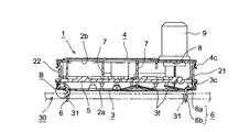
発明の実施の形態を図面を参照しつつ説明すると、図1は本発明の実施形態例に係る電子回路モジュールを上方から見た斜視図、図2は該モジュールの底面図、図3は図2のA−A線に沿う断面図、図4は図3のB部拡大図、図5は該モジュールを下方から見た斜視図、図6は図5のC部拡大図、図7は図5に示す該モジュールから下カバーを取り外した状態を示す斜視図である。 An embodiment of the invention will be described with reference to the drawings. FIG. 1 is a perspective view of an electronic circuit module according to an embodiment of the present invention as viewed from above, FIG. 2 is a bottom view of the module, and FIG. FIG. 4 is an enlarged view of part B of FIG. 3, FIG. 5 is a perspective view of the module viewed from below, FIG. 6 is an enlarged view of part C of FIG. 5, and FIG. It is a perspective view which shows the state which removed the lower cover from this module shown in FIG.
これらの図に示す電子回路モジュール1は、マザーボード30(図3参照)上に実装されてデジタル放送等のチューナとして使用されるものである。この電子回路モジュール1は、枠体2と下カバー3と上カバー4とを組み合わせて筐体が構成され、この筐体の内部空間に、高周波回路が設けられた回路基板5が設置されている。
The
枠体2は比較的肉厚な金属板からなる4枚の側板21,22,23,24を方形枠状に配設して主に構成されており、これら側板21〜24の下端部によって下部開放端2aが画成され、側板21〜24の上端部によって上部開放端2bが画成されている。また、枠体2には下部開放端2aの四隅近傍に、側板21,22の下端の計4箇所から内方へL字状に延出する取付脚6が設けられている。各取付脚6は、側板21(または22)の下端から内方へ延びる連結部6aと、連結部6aの先端から下方へ突出する突出部6bとからなる折曲片であって、金属板からプレス抜きされた段階で側板21(または22)に延設されている舌片を折り曲げ加工して形成されたものである。これら取付脚6は、その突出部6bが下カバー3を貫通してマザーボード30の取付孔31(図3参照)に挿通され、このマザーボード30の図示せぬ接地用パターンに半田付けされるようになっている。なお、図3に示すように、側板21〜24には、内部空間を仕切る仕切り板7と、同軸コネクタ9を支持する支持板8とが一体化されており、これら仕切り板7および支持板8も金属板からなり枠体2を構成している。
The
下カバー3は側板21〜24よりも肉薄な金属板からなり、この下カバー3が下部開放端2aを蓋閉して枠体2の下端部に嵌着されている。下カバー3は、下部開放端2aと対向する矩形状の底板部3aと、この底板部3aの各辺に連続する帯状の曲げ代部3bから上向きに突出する複数の弾性片3cとを有しており、底板部3aの周縁のほぼ全周に沿って弾性片3cが配設されている。これら弾性片3cを撓ませながら枠体2の下端部(側板21〜24の下端部)に外嵌させることによって、下カバー3は枠体2に取り付けられている。また、底板部3aの四隅近傍には透孔3dが開設されていると共に、側板23寄りに配置される2つの透孔3dと隣接する2箇所に突起3eが上向きに突設されている。そして、下カバー3を枠体2の下端部に嵌着させると、各透孔3dに枠体2の各取付脚6の突出部6bが挿通されると共に、各突起3eが、隣接する透孔3dに突出部6bが挿通された取付脚6の連結部6aと対向して該連結部6aに当接する(図4参照)。なお、底板部3aに形成されている切り起こし部3fを介して、仕切り板7が下ケース3と接触するようになっている。
The
上カバー4も下カバー3と同様に側板21〜24よりも肉薄な金属板からなり、この上カバー4が上部開放端2bを蓋閉して枠体2の上端部に嵌着されている。上カバー4は、上部開放端2bと対向する矩形状の天板部4aと、この天板部4aの各辺に連続する帯状の曲げ代部4bから下向きに突出する複数の弾性片4cとを有しており、天板部4aの周縁のほぼ全周に沿って弾性片4cが配設されている。これら弾性片4cを撓ませながら枠体2の上端部(側板21〜24の上端部)に外嵌させることによって、上カバー4は枠体2に取り付けられている。なお、天板部4aの一隅には、支持板8に支持された同軸コネクタ9が固設されて上方に突出している。
Similarly to the
回路基板5は図示せぬ配線パターンや電子部品を配設して高周波回路を構成しており、例えばRF回路部とOSC回路部との間に仕切り板7が立設されるようになっている。この回路基板5は、側板21〜24に囲繞された位置決め状態で枠体2に支持されており、側板24と隣接する回路基板5の一辺端部において複数本のピン端子10が前記配線パターンと接続されている。また、同軸コネクタ9の中心導体も該配線パターンに接続されている。ピン端子10群は枠体2の外方へ突出して下向きに折曲されており、マザーボード30の図示せぬ接続ランド群にピン端子10群を半田付けすることによって、回路基板5の高周波回路がマザーボード30側の外部回路と接続されるようになっている。
The
このように本実施形態例に係る電子回路モジュール1は、枠体2の下端部に設けた各取付脚6が側板21(または22)から内方へ延びて下方へ突出するというL字状に形成されているため、下カバー3には周縁部から内方へずらした位置に取付脚6の突出部6bを挿通させるための透孔3dを開設しておけばよく、それゆえ下カバー3の周縁部には透孔3dの有無に拘らず弾性片3cを設けることができる。そして、下カバー3の透孔3dの周辺に弾性片3cを設けても、該弾性片3cが組立時に取付脚6と干渉する虞は少なく、かつ透孔3dの周辺であっても所要の弾発力を生起する弾性片3cを形成することは容易である。したがって、この電子回路モジュール1では、下カバー3の周縁部のほぼ全周に亘って所要の弾発力を生起する弾性片3cを設けており、その結果、枠体2に対する下カバー3の嵌合強度が高まって、下カバー3に起因するラットルノイズが発生しにくく、下カバー3の脱落事故も回避しやすくなっている。なお、上カバー4の周縁部にも、ほぼ全周に亘って所要の弾発力を生起する弾性片4cが設けてあるので、枠体2に対する上カバー4の嵌合強度も高い。
As described above, the
また、この電子回路モジュール1の取付脚6の突出部6bが挿通されるマザーボード30の取付孔31は、該電子回路モジュール1の実装領域の周縁よりも内側に位置することになるので、電子回路モジュール1はマザーボード30上の周縁部であっても支障なく実装することが可能で実装位置の制約が少ない。それゆえ、マザーボード30の配線レイアウトの設計自由度が向上して高密度実装が図りやすくなっている。
Further, the mounting
また、この電子回路モジュール1は、側板21,22に設けられた取付脚6が比較的肉厚な金属板からなるため、組立時などに取付脚6が不所望に変形する虞は少ない。しかも、枠体2の一部である取付脚6がマザーボード30に半田付けされるため、同軸コネクタ9に図示せぬアンテナコネクタを着脱させる際などに作用する外力に対して強く、所要の信頼性が確保されている。
In the
さらに、この電子回路モジュール1では、下カバー3の2つの透孔3dの近傍に突起3eを設け、これら突起3eをそれぞれ対向する取付脚6の連結部6aに当接させているため、取付脚6を介して下カバー3をマザーボード30の接地用パターンと確実に導通させることができる。それゆえ、下カバー3が接地板として効果的に活用できるようになっている。ただし、下カバー3に突起3eを設ける代わりに、取付脚6の連結部6aに下向きの突起を設けて該突起を下カバー3の透孔3d近傍に当接させるようにしてもよい。
Further, in this
なお、L字状の取付脚6は側板21〜24の適宜箇所に必要数だけ設けることができるが、上記実施形態例のように、取付脚6が枠体2の下部開放端2aの四隅近傍に配設されていると、これら4片の取付脚6によって電子回路モジュール1の姿勢を安定させることができるため好適である。
Note that the required number of L-shaped mounting
1 電子回路モジュール
2 枠体
2a 下部開放端
3 下カバー
3c 弾性片
3d 透孔
3e 突起
4 上カバー
5 回路基板
6 取付脚
6a 連結部
6b 突出部
9 同軸コネクタ
21〜24 側板
30 マザーボード
31 取付孔
DESCRIPTION OF
Claims (3)
前記枠体の下端部の複数箇所に、前記側板から内方へ延びて下方へ突出するL字状の取付脚を設け、これら取付脚の突出部分が前記カバーに設けた透孔を貫通して前記マザーボードに半田付けされるようにしたことを特徴とする電子回路モジュール。 A frame having a side plate made of a metal plate disposed in a rectangular frame shape, a circuit board supported by the frame in a state surrounded by the side plate, and a plurality of elastic pieces projecting upward at the peripheral edge And a cover that is attached to the lower open end of the frame body in a state where the elastic pieces are elastically contacted to the outer surface of the side plate. An electronic circuit module that is mounted and used,
L-shaped mounting legs that extend inward from the side plate and protrude downward are provided at a plurality of locations on the lower end of the frame, and the protruding portions of the mounting legs penetrate through the through holes provided in the cover. An electronic circuit module, wherein the electronic circuit module is soldered to the mother board.
Priority Applications (4)
| Application Number | Priority Date | Filing Date | Title |
|---|---|---|---|
| JP2007242759A JP4890400B2 (en) | 2007-09-19 | 2007-09-19 | Electronic circuit module |
| TW097132548A TW200922439A (en) | 2007-09-19 | 2008-08-26 | Electronic circuit mould |
| KR1020080091589A KR20090030234A (en) | 2007-09-19 | 2008-09-18 | Electronic circuit module |
| CNA2008101656188A CN101394725A (en) | 2007-09-19 | 2008-09-19 | Electronic circuit mould |
Applications Claiming Priority (1)
| Application Number | Priority Date | Filing Date | Title |
|---|---|---|---|
| JP2007242759A JP4890400B2 (en) | 2007-09-19 | 2007-09-19 | Electronic circuit module |
Publications (2)
| Publication Number | Publication Date |
|---|---|
| JP2009076594A true JP2009076594A (en) | 2009-04-09 |
| JP4890400B2 JP4890400B2 (en) | 2012-03-07 |
Family
ID=40494729
Family Applications (1)
| Application Number | Title | Priority Date | Filing Date |
|---|---|---|---|
| JP2007242759A Expired - Fee Related JP4890400B2 (en) | 2007-09-19 | 2007-09-19 | Electronic circuit module |
Country Status (4)
| Country | Link |
|---|---|
| JP (1) | JP4890400B2 (en) |
| KR (1) | KR20090030234A (en) |
| CN (1) | CN101394725A (en) |
| TW (1) | TW200922439A (en) |
Cited By (2)
| Publication number | Priority date | Publication date | Assignee | Title |
|---|---|---|---|---|
| KR101392690B1 (en) | 2013-02-27 | 2014-05-07 | 쌍용자동차 주식회사 | Multi-layer pcb combined module for automobile |
| JP2015095684A (en) * | 2013-11-08 | 2015-05-18 | 株式会社オートネットワーク技術研究所 | Noise filter |
Families Citing this family (3)
| Publication number | Priority date | Publication date | Assignee | Title |
|---|---|---|---|---|
| JP5103414B2 (en) * | 2009-02-06 | 2012-12-19 | アルプス電気株式会社 | High frequency unit |
| JP2012191009A (en) * | 2011-03-10 | 2012-10-04 | Alps Electric Co Ltd | Electronic circuit unit and method of manufacturing the same |
| JP6122372B2 (en) * | 2013-09-27 | 2017-04-26 | 新光電気工業株式会社 | Electronic component case and electronic component device |
Citations (4)
| Publication number | Priority date | Publication date | Assignee | Title |
|---|---|---|---|---|
| JPS62168690A (en) * | 1986-01-21 | 1987-07-24 | Toshiba Corp | Laser cutting method for thick plate |
| JPH048494A (en) * | 1990-04-27 | 1992-01-13 | Canon Inc | Fine adjustment device for industrial robot position detecting means |
| JP2000196256A (en) * | 1998-12-25 | 2000-07-14 | Alps Electric Co Ltd | Electronic equipment and its manufacture |
| JP2006278962A (en) * | 2005-03-30 | 2006-10-12 | Alps Electric Co Ltd | Electronic circuit unit |
-
2007
- 2007-09-19 JP JP2007242759A patent/JP4890400B2/en not_active Expired - Fee Related
-
2008
- 2008-08-26 TW TW097132548A patent/TW200922439A/en not_active IP Right Cessation
- 2008-09-18 KR KR1020080091589A patent/KR20090030234A/en active IP Right Grant
- 2008-09-19 CN CNA2008101656188A patent/CN101394725A/en active Pending
Patent Citations (4)
| Publication number | Priority date | Publication date | Assignee | Title |
|---|---|---|---|---|
| JPS62168690A (en) * | 1986-01-21 | 1987-07-24 | Toshiba Corp | Laser cutting method for thick plate |
| JPH048494A (en) * | 1990-04-27 | 1992-01-13 | Canon Inc | Fine adjustment device for industrial robot position detecting means |
| JP2000196256A (en) * | 1998-12-25 | 2000-07-14 | Alps Electric Co Ltd | Electronic equipment and its manufacture |
| JP2006278962A (en) * | 2005-03-30 | 2006-10-12 | Alps Electric Co Ltd | Electronic circuit unit |
Cited By (2)
| Publication number | Priority date | Publication date | Assignee | Title |
|---|---|---|---|---|
| KR101392690B1 (en) | 2013-02-27 | 2014-05-07 | 쌍용자동차 주식회사 | Multi-layer pcb combined module for automobile |
| JP2015095684A (en) * | 2013-11-08 | 2015-05-18 | 株式会社オートネットワーク技術研究所 | Noise filter |
Also Published As
| Publication number | Publication date |
|---|---|
| CN101394725A (en) | 2009-03-25 |
| TW200922439A (en) | 2009-05-16 |
| JP4890400B2 (en) | 2012-03-07 |
| KR20090030234A (en) | 2009-03-24 |
| TWI372018B (en) | 2012-09-01 |
Similar Documents
| Publication | Publication Date | Title |
|---|---|---|
| US7922534B2 (en) | Socket connector | |
| US8070517B2 (en) | Electrical connector having an improved spring member for abutting against a metal plate | |
| US20090159329A1 (en) | Electrical Device | |
| JP2014033025A (en) | Electronic circuit module | |
| JP4348725B2 (en) | Socket for mounting electronic parts | |
| US20090268420A1 (en) | Shielding assembly | |
| JP4890400B2 (en) | Electronic circuit module | |
| US11431130B2 (en) | Electrical connector assembly with metallic cage having elastic grounding fingers around the mounting portion | |
| US8558121B2 (en) | Electronic device having an electromagnetic shield | |
| US9190779B2 (en) | Electrical connector having better electrical performance | |
| JP4476311B2 (en) | connector | |
| JP4674527B2 (en) | Shield structure | |
| JP2009141057A (en) | Electronic equipment and slot | |
| JP4682646B2 (en) | Implementation body | |
| JP3990634B2 (en) | Shielded electrical connector for printed circuit board mounting | |
| JP2006286456A (en) | Connector for flexible board | |
| US8337232B2 (en) | Electrical connector having a shielding in an opening in its base | |
| JP2009158548A (en) | Shielding case, wiring board and electronic component module | |
| JP4477660B2 (en) | Camera module socket | |
| US20100238641A1 (en) | Shield structure of a tuner apparatus | |
| JP3892189B2 (en) | Electromagnetic wave shielding structure of electronic circuit board | |
| JP5538346B2 (en) | Antenna terminal structure and tuner device including the same | |
| JP3127153U (en) | A shield device that prevents electromagnetic noise. | |
| JP2004241304A (en) | Electronic connector | |
| JP2009129653A (en) | Antenna terminal structure, and tuner device equipped with the same |
Legal Events
| Date | Code | Title | Description |
|---|---|---|---|
| A621 | Written request for application examination |
Free format text: JAPANESE INTERMEDIATE CODE: A621 Effective date: 20100611 |
|
| A977 | Report on retrieval |
Free format text: JAPANESE INTERMEDIATE CODE: A971007 Effective date: 20111130 |
|
| TRDD | Decision of grant or rejection written | ||
| A01 | Written decision to grant a patent or to grant a registration (utility model) |
Free format text: JAPANESE INTERMEDIATE CODE: A01 Effective date: 20111206 |
|
| A01 | Written decision to grant a patent or to grant a registration (utility model) |
Free format text: JAPANESE INTERMEDIATE CODE: A01 |
|
| A61 | First payment of annual fees (during grant procedure) |
Free format text: JAPANESE INTERMEDIATE CODE: A61 Effective date: 20111214 |
|
| R150 | Certificate of patent or registration of utility model |
Free format text: JAPANESE INTERMEDIATE CODE: R150 |
|
| FPAY | Renewal fee payment (event date is renewal date of database) |
Free format text: PAYMENT UNTIL: 20141222 Year of fee payment: 3 |
|
| LAPS | Cancellation because of no payment of annual fees |