JP2008522446A - Method and apparatus for controlling spatial temperature distribution - Google Patents
Method and apparatus for controlling spatial temperature distribution Download PDFInfo
- Publication number
- JP2008522446A JP2008522446A JP2007544574A JP2007544574A JP2008522446A JP 2008522446 A JP2008522446 A JP 2008522446A JP 2007544574 A JP2007544574 A JP 2007544574A JP 2007544574 A JP2007544574 A JP 2007544574A JP 2008522446 A JP2008522446 A JP 2008522446A
- Authority
- JP
- Japan
- Prior art keywords
- temperature
- chuck
- flat support
- workpiece
- base
- Prior art date
- Legal status (The legal status is an assumption and is not a legal conclusion. Google has not performed a legal analysis and makes no representation as to the accuracy of the status listed.)
- Pending
Links
Images


Classifications
-
- H—ELECTRICITY
- H01—ELECTRIC ELEMENTS
- H01L—SEMICONDUCTOR DEVICES NOT COVERED BY CLASS H10
- H01L21/00—Processes or apparatus adapted for the manufacture or treatment of semiconductor or solid state devices or of parts thereof
- H01L21/67—Apparatus specially adapted for handling semiconductor or electric solid state devices during manufacture or treatment thereof; Apparatus specially adapted for handling wafers during manufacture or treatment of semiconductor or electric solid state devices or components ; Apparatus not specifically provided for elsewhere
- H01L21/683—Apparatus specially adapted for handling semiconductor or electric solid state devices during manufacture or treatment thereof; Apparatus specially adapted for handling wafers during manufacture or treatment of semiconductor or electric solid state devices or components ; Apparatus not specifically provided for elsewhere for supporting or gripping
-
- H—ELECTRICITY
- H01—ELECTRIC ELEMENTS
- H01L—SEMICONDUCTOR DEVICES NOT COVERED BY CLASS H10
- H01L21/00—Processes or apparatus adapted for the manufacture or treatment of semiconductor or solid state devices or of parts thereof
- H01L21/67—Apparatus specially adapted for handling semiconductor or electric solid state devices during manufacture or treatment thereof; Apparatus specially adapted for handling wafers during manufacture or treatment of semiconductor or electric solid state devices or components ; Apparatus not specifically provided for elsewhere
- H01L21/67005—Apparatus not specifically provided for elsewhere
- H01L21/67242—Apparatus for monitoring, sorting or marking
- H01L21/67248—Temperature monitoring
-
- H—ELECTRICITY
- H01—ELECTRIC ELEMENTS
- H01J—ELECTRIC DISCHARGE TUBES OR DISCHARGE LAMPS
- H01J37/00—Discharge tubes with provision for introducing objects or material to be exposed to the discharge, e.g. for the purpose of examination or processing thereof
- H01J37/32—Gas-filled discharge tubes
- H01J37/32431—Constructional details of the reactor
- H01J37/32715—Workpiece holder
- H01J37/32724—Temperature
-
- H—ELECTRICITY
- H01—ELECTRIC ELEMENTS
- H01L—SEMICONDUCTOR DEVICES NOT COVERED BY CLASS H10
- H01L21/00—Processes or apparatus adapted for the manufacture or treatment of semiconductor or solid state devices or of parts thereof
- H01L21/67—Apparatus specially adapted for handling semiconductor or electric solid state devices during manufacture or treatment thereof; Apparatus specially adapted for handling wafers during manufacture or treatment of semiconductor or electric solid state devices or components ; Apparatus not specifically provided for elsewhere
- H01L21/67005—Apparatus not specifically provided for elsewhere
- H01L21/67011—Apparatus for manufacture or treatment
- H01L21/67017—Apparatus for fluid treatment
- H01L21/67063—Apparatus for fluid treatment for etching
- H01L21/67069—Apparatus for fluid treatment for etching for drying etching
-
- H—ELECTRICITY
- H01—ELECTRIC ELEMENTS
- H01L—SEMICONDUCTOR DEVICES NOT COVERED BY CLASS H10
- H01L21/00—Processes or apparatus adapted for the manufacture or treatment of semiconductor or solid state devices or of parts thereof
- H01L21/67—Apparatus specially adapted for handling semiconductor or electric solid state devices during manufacture or treatment thereof; Apparatus specially adapted for handling wafers during manufacture or treatment of semiconductor or electric solid state devices or components ; Apparatus not specifically provided for elsewhere
- H01L21/67005—Apparatus not specifically provided for elsewhere
- H01L21/67011—Apparatus for manufacture or treatment
- H01L21/67098—Apparatus for thermal treatment
- H01L21/67103—Apparatus for thermal treatment mainly by conduction
-
- H—ELECTRICITY
- H01—ELECTRIC ELEMENTS
- H01L—SEMICONDUCTOR DEVICES NOT COVERED BY CLASS H10
- H01L21/00—Processes or apparatus adapted for the manufacture or treatment of semiconductor or solid state devices or of parts thereof
- H01L21/67—Apparatus specially adapted for handling semiconductor or electric solid state devices during manufacture or treatment thereof; Apparatus specially adapted for handling wafers during manufacture or treatment of semiconductor or electric solid state devices or components ; Apparatus not specifically provided for elsewhere
- H01L21/683—Apparatus specially adapted for handling semiconductor or electric solid state devices during manufacture or treatment thereof; Apparatus specially adapted for handling wafers during manufacture or treatment of semiconductor or electric solid state devices or components ; Apparatus not specifically provided for elsewhere for supporting or gripping
- H01L21/6831—Apparatus specially adapted for handling semiconductor or electric solid state devices during manufacture or treatment thereof; Apparatus specially adapted for handling wafers during manufacture or treatment of semiconductor or electric solid state devices or components ; Apparatus not specifically provided for elsewhere for supporting or gripping using electrostatic chucks
- H01L21/6833—Details of electrostatic chucks
-
- H—ELECTRICITY
- H01—ELECTRIC ELEMENTS
- H01L—SEMICONDUCTOR DEVICES NOT COVERED BY CLASS H10
- H01L21/00—Processes or apparatus adapted for the manufacture or treatment of semiconductor or solid state devices or of parts thereof
- H01L21/67—Apparatus specially adapted for handling semiconductor or electric solid state devices during manufacture or treatment thereof; Apparatus specially adapted for handling wafers during manufacture or treatment of semiconductor or electric solid state devices or components ; Apparatus not specifically provided for elsewhere
- H01L21/683—Apparatus specially adapted for handling semiconductor or electric solid state devices during manufacture or treatment thereof; Apparatus specially adapted for handling wafers during manufacture or treatment of semiconductor or electric solid state devices or components ; Apparatus not specifically provided for elsewhere for supporting or gripping
- H01L21/687—Apparatus specially adapted for handling semiconductor or electric solid state devices during manufacture or treatment thereof; Apparatus specially adapted for handling wafers during manufacture or treatment of semiconductor or electric solid state devices or components ; Apparatus not specifically provided for elsewhere for supporting or gripping using mechanical means, e.g. chucks, clamps or pinches
- H01L21/68714—Apparatus specially adapted for handling semiconductor or electric solid state devices during manufacture or treatment thereof; Apparatus specially adapted for handling wafers during manufacture or treatment of semiconductor or electric solid state devices or components ; Apparatus not specifically provided for elsewhere for supporting or gripping using mechanical means, e.g. chucks, clamps or pinches the wafers being placed on a susceptor, stage or support
-
- H—ELECTRICITY
- H01—ELECTRIC ELEMENTS
- H01J—ELECTRIC DISCHARGE TUBES OR DISCHARGE LAMPS
- H01J2237/00—Discharge tubes exposing object to beam, e.g. for analysis treatment, etching, imaging
- H01J2237/20—Positioning, supporting, modifying or maintaining the physical state of objects being observed or treated
- H01J2237/2001—Maintaining constant desired temperature
-
- H—ELECTRICITY
- H01—ELECTRIC ELEMENTS
- H01J—ELECTRIC DISCHARGE TUBES OR DISCHARGE LAMPS
- H01J2237/00—Discharge tubes exposing object to beam, e.g. for analysis treatment, etching, imaging
- H01J2237/32—Processing objects by plasma generation
- H01J2237/33—Processing objects by plasma generation characterised by the type of processing
- H01J2237/334—Etching
Abstract
【課題】反応性イオンエッチング及び同様な加工中半導体ウェーハの温度を制御する方法及び装置を提供する。
【解決手段】プラズマ加工装置用のチャックは、温度制御式ベースと、断熱材と、フラット支持体と、加熱器とを含む。温度制御式ベースは、操作中、加工物の望ましい温度以下の温度に制御される。断熱材は、温度制御式ベースの少なくとも一部分に上に配置される。フラット支持体は、加工物を保持し且つ断熱材の上に配置される。加熱器は、フラット支持体内に埋め込まれ及び又はフラット支持体の下側に取り付けられる。加熱器は、複数の対応する加熱ゾーンを加熱する複数の加熱素子を含む。各加熱素子に供給される電力及び又は各々の加熱素子の温度は、独立に制御される。加熱器及びフラット支持体は、毎秒少なくとも1℃の組合せ温度割合変化を有する。
【選択図】図1A method and apparatus for controlling the temperature of a semiconductor wafer during reactive ion etching and similar processing.
A chuck for a plasma processing apparatus includes a temperature-controlled base, a heat insulating material, a flat support, and a heater. The temperature controlled base is controlled to a temperature below the desired temperature of the workpiece during operation. Thermal insulation is disposed on at least a portion of the temperature controlled base. A flat support holds the workpiece and is placed over the insulation. The heater is embedded in the flat support and / or attached to the underside of the flat support. The heater includes a plurality of heating elements that heat a plurality of corresponding heating zones. The power supplied to each heating element and / or the temperature of each heating element is controlled independently. The heater and flat support have a combined temperature rate change of at least 1 ° C. per second.
[Selection] Figure 1
Description
本発明は、基板支持体に関する。特に、本発明は、プラズマ加工中基板内に均一温度分布を達成するための方法及び装置に関する。 The present invention relates to a substrate support. In particular, the present invention relates to a method and apparatus for achieving a uniform temperature distribution within a substrate during plasma processing.
代表的なプラズマエッチング装置は、リアクタを含み、該リアクタには、反応ガス或いは複数の反応ガスが流れるチャンバが存在する。ガスは、チャンバ内で、典型的には高周波エネルギーによってプラズマの中へイオン化される。プラズマガスの極めて反応性が高いイオンは、集積回路(IC)に加工される半導体ウェーハ表面のポリマーマスクのような材料と反応することができる。エッチングの前に、ウェーハは、チャンバ内に配置され、ウェーハの上面をプラズマに露出させるチャック或いはホルダーによって適当な位置に保持される。いくつかの種類のチャック(サセプタとも呼ばれる)がこの技術分野で知られている。チャックは、等温面を提供し且つプラズマによってウェーハに与えられた熱を除去する、ウェーハのためのヒートシンクとして役立つ。或る種類のチャックでは、半導体ウェーハは、機械的クランプ手段によりエッチングのために適所に保持される。別の種類のチャックでは、半導体ウェーハは、チャックとウェーハとの間の電界によって発生される静電気力により適所に保持される。本発明は、両方の種類のチャックに適用することができる。 A typical plasma etching apparatus includes a reactor, and the reactor has a chamber through which a reaction gas or a plurality of reaction gases flow. The gas is ionized into the plasma within the chamber, typically by radio frequency energy. The extremely reactive ions of the plasma gas can react with materials such as a polymer mask on the surface of a semiconductor wafer that is processed into an integrated circuit (IC). Prior to etching, the wafer is placed in the chamber and held in place by a chuck or holder that exposes the top surface of the wafer to the plasma. Several types of chucks (also called susceptors) are known in the art. The chuck serves as a heat sink for the wafer, providing an isothermal surface and removing the heat imparted to the wafer by the plasma. In one type of chuck, the semiconductor wafer is held in place for etching by mechanical clamping means. In another type of chuck, the semiconductor wafer is held in place by electrostatic forces generated by the electric field between the chuck and the wafer. The present invention can be applied to both types of chucks.
代表的なプラズマエッチング操作では、プラズマガスの反応性イオンは、半導体ウェーハ面の材料の一部と化学的に反応する。ある加工は、ウェーハにある程度の加熱を引き起すが、加熱のほとんどは、プラズマによって引き起される。他方、プラズマ(イオン及びラジカル)とウェーハ材料との間の反応は、ウェーハの温度上昇によってある程度まで加速される。ウェーハ上の各微視的な点におけるウェーハの局部的温度及び反応速度は、ウェーハの面積を横切るウェーハの温度があまりにも変化するならばウェーハの面の上の材料のエッチングの有害なむらが容易に生ずることがある程度に関係する。ほとんどの場合、エッチングがほぼ完璧な程度に均一であることが極力望ましい。そうでなければ、製造される集積回路装置(IC)は、望ましい基準から外れる電子特性を有する。更に、ウェーハ径の大きさが増すごとに、より大きなウェーハからICの各バッチの均一性を確保することの問題がさらに難しくなる。その他の場合には、カスタムプロフィールを得るためにウェーハの表面温度を制御することができることが望ましい。 In a typical plasma etching operation, the reactive ions of the plasma gas chemically react with a portion of the material on the semiconductor wafer surface. Some processes cause some heating to the wafer, but most of the heating is caused by the plasma. On the other hand, the reaction between the plasma (ions and radicals) and the wafer material is accelerated to some extent by the temperature increase of the wafer. The local temperature and reaction rate of the wafer at each microscopic point on the wafer facilitates deleterious uneven etching of the material on the surface of the wafer if the temperature of the wafer across the wafer area changes too much To some extent. In most cases, it is desirable to be as uniform as possible with almost perfect etching. Otherwise, the manufactured integrated circuit device (IC) has electronic characteristics that deviate from the desired criteria. Further, as the wafer diameter increases, the problem of ensuring uniformity of each batch of ICs from a larger wafer becomes more difficult. In other cases, it is desirable to be able to control the surface temperature of the wafer to obtain a custom profile.
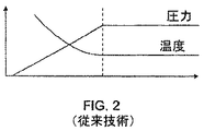
反応性イオンエッチング(RIE)中ウェーハの温度上昇の問題は、よく知られており、RIE中ウェーハの温度を制御するいろいろな試みが過去になされてきた。図1は、RIE中ウェーハ温度を制御するための一つの方法を示す。(ヘリウムのような)冷却ガスが、ウェーハ104の底とウェーハ104を保持するチャック106の上面との間の単一の薄い空間102内に単一の圧力で入れられる。
The problem of wafer temperature rise during reactive ion etching (RIE) is well known, and various attempts have been made in the past to control the temperature of the wafer during RIE. FIG. 1 illustrates one method for controlling wafer temperature during RIE. A cooling gas (such as helium) is introduced at a single pressure into a single
一般的に、冷却材漏れを減らすためにチャック106の外縁で約1mmないし約5mm延びる平滑密封ランドを除いてチャック外周部にはOリング或いは他の縁シールがない。必然的に、エラストマーシールなしでは、密封ランド全体にわたって顕著な漸進的圧力損失があり、ウェーハ104の縁が不適当に冷却されるかもしれない。従って、ウェーハ104の縁の近くに当たる熱流108は、チャックに効果的に導かれる前にかなり半径方向内方に流れなければならない。ウェーハ104の上の矢印106は、ウェーハ104を加熱する入り熱流を示す。ウェーハ104の中の熱の流れは、矢印110で示される。これは、チャックの縁帯域が何故表面の残部よりも常に熱くなる傾向があるかを説明する。図2は、ウェーハ104の代表的な温度分布を示す。ウェーハ104の周辺部分の圧力損失により、ウェーハ104の周辺部分がさらに熱くなる。
Generally, there is no O-ring or other edge seal on the outer periphery of the chuck except for a smooth sealing land that extends from about 1 mm to about 5 mm at the outer edge of the
ゾーン冷却の必要性に対処する一つの方法は、局部的な接触面積を効果的に変えるために表面粗さを変化させること或いはレリーフ(浮彫り)パターンを切ることにある。係る方式は、全く背面冷却材ガスなしで用いることができ、その場合には、接触面積、表面粗さ、及びクランプ力が熱伝導を決める。しかしながら、局部的な接触面積は、チャックを再加工することによってのみ調整することができる。ゾーン冷却の必要性に対処する別の方法は、冷却材ガスを用い、熱移動を増やしかつ微調整するために冷却材ガスの圧力を変えることである。しかしながら、レリーフパターンは、依然として実質的に固定される。チャックの表面を、ディバイダとしての小さい密封ランドの有無に関わらず、異なるゾーンに分割することによって、且つ別々の冷却ガスを各ゾーンに供給することによって、かなりの程度の独立の空間制御を達成しうる。各ゾーンへのガス供給は、異なる組成を有してもよいし、或いは異なる圧力に設定されてもよい、かくして熱伝導を変化させる。各ゾーンの作動条件は、レシピ制御の下に設定されてもよいし、或いは各加工段階中動的に安定化されてもよい。係る方式は、プラズマからの入り熱流を再分配し且つそれを異なる領域に引き出すことに依存する。これは、高電力熱流で比較的有効であるが、低電力熱流では小さな温度差を与えるだけである。例えば、約1W/cm2の均一熱流及び約3mmの密封ランドでは、ウェーハ周辺近くで10℃ないし30℃の温度増加に導く中心ないしエッジの熱勾配を得ることが可能である。この大きさの熱勾配は、加工制御パラメータとして非常に効果的でありうる。しかしながら、他の加工が低電力で行なわれてもよく、例えばポリゲート加工がほんの0.2W/cm2の熱流を有してもよい。非常に制御しにくく且つ不適当な全体冷却をもたらす傾向がある、平均伝導を極端に低くしない限り、典型的には5℃以下の非常に小さな差が存在だけである。 One way to address the need for zone cooling is to change the surface roughness or cut the relief pattern to effectively change the local contact area. Such a scheme can be used without any backside coolant gas, in which case the contact area, surface roughness, and clamping force determine the heat conduction. However, the local contact area can only be adjusted by reworking the chuck. Another way to address the need for zone cooling is to use coolant gas and vary the pressure of the coolant gas to increase and fine tune heat transfer. However, the relief pattern is still substantially fixed. A considerable degree of independent spatial control is achieved by dividing the surface of the chuck into different zones with or without a small sealed land as a divider and by supplying separate cooling gases to each zone. sell. The gas supply to each zone may have a different composition or may be set to a different pressure, thus changing the heat transfer. The operating conditions of each zone may be set under recipe control or may be dynamically stabilized during each processing stage. Such a scheme relies on redistributing the incoming heat flow from the plasma and drawing it to different regions. This is relatively effective at high power heat flow, but only gives a small temperature difference at low power heat flow. For example, with a uniform heat flow of about 1 W / cm 2 and a sealed land of about 3 mm, it is possible to obtain a center-to-edge thermal gradient leading to a temperature increase of 10 ° C. to 30 ° C. near the wafer periphery. A thermal gradient of this magnitude can be very effective as a process control parameter. However, other processing may be performed at low power, for example, polygate processing may have a heat flow of only 0.2 W / cm 2 . There is typically only a very small difference of 5 ° C. or less unless the average conduction is extremely low, which is very difficult to control and tends to result in inadequate overall cooling.
従って、かなりのプラズマ熱流を要求することなく反応性イオンエッチング及び同様な加工中半導体ウェーハの温度を制御するための方法及び装置の要求が存在する。本発明の主要な目的は、これらの要求を解決し且つ関連した利点を更に提供することにある。 Accordingly, there is a need for a method and apparatus for controlling the temperature of a semiconductor wafer during reactive ion etching and similar processing without requiring significant plasma heat flow. The main objective of the present invention is to solve these requirements and provide further related advantages.
プラズマ加工装置のためのチャックは、温度制御式ベースと、断熱材と、フラット支持体と、加熱器と、を含む。温度制御式ベースは、操作中、加工物の望ましい温度以下の温度に制御される。断熱材は、温度制御式ベースの少なくとも一部分の上に配置される。フラット支持体は、加工物を保持し且つ断熱材の上に配置される。加熱器は、フラット支持体内に埋め込まれ及び又はフラット支持体の下側に取り付けられる。加熱器は、複数の対応する加熱ゾーンを加熱する複数の加熱素子を含む。各加熱素子に供給される電力及び又は各加熱素子の温度は、独立に制御される。加熱器及びフラット支持体は、毎秒少なくとも1℃の組合せ温度割合変化を有する。 A chuck for a plasma processing apparatus includes a temperature-controlled base, a heat insulating material, a flat support, and a heater. The temperature controlled base is controlled to a temperature below the desired temperature of the workpiece during operation. The insulation is disposed on at least a portion of the temperature controlled base. A flat support holds the workpiece and is placed over the insulation. The heater is embedded in the flat support and / or attached to the underside of the flat support. The heater includes a plurality of heating elements that heat a plurality of corresponding heating zones. The power supplied to each heating element and / or the temperature of each heating element is controlled independently. The heater and flat support have a combined temperature rate change of at least 1 ° C. per second.
本発明の実施形態を加工物支持体に関連してここに記述する。当業者は、本発明の以下の詳細な説明が単に例証であり、いかなる意味においても限定になるものではない、ということを認識するであろう。本発明の他の実施形態は、それ自体をこの開示の利益を有するそのような当業者に容易に思付かせるであろう。今、添付図面に図示されるように本発明の実施例を詳細に参照する。同じ或いは同様の部分を示すために、図面及び以下の詳細な説明全体を通して同じ参照表示が用いられる。 Embodiments of the present invention are described herein in connection with a workpiece support. Those skilled in the art will recognize that the following detailed description of the present invention is merely illustrative and not limiting in any way. Other embodiments of the invention will readily come to mind to those skilled in the art having the benefit of this disclosure per se. Reference will now be made in detail to embodiments of the present invention as illustrated in the accompanying drawings. The same reference designations are used throughout the drawings and the following detailed description to refer to the same or like parts.
明瞭にするために、ここに記述される実施のごく普通の部分の全ては示されていないし又記述されてもいない。勿論、そのような実際の実施の開発において、多くの実施−特別の決定を、アプリケーション−及びビジネス関連制約の順守のような、開発者の特別の目標を達成するために行なわなければならないし、これらの特別の目標は、その実施により(一つの実施から別の実施まで)及びその開発者により(一人の開発者から別の開発者まで)変化するであろう、ということが理解されるであろう。さらに、そのような開発の努力は、複雑であり時間がかかるが、それにもかかわらず、この開示の利益を有する当業者にとっては、エンジニアリングの日常の仕事になるということが理解されるであろう。 For the sake of clarity, not all of the routine parts of the implementation described herein are shown or described. Of course, in the development of such an actual implementation, many implementation-specific decisions must be made to achieve the developer's special goals, such as compliance with application- and business-related constraints, It is understood that these special goals will vary from implementation to implementation (from one implementation to another) and from the developer (from one developer to another). I will. Further, it will be appreciated that such development efforts are complex and time consuming, but nevertheless will be a routine engineering task for those skilled in the art having the benefit of this disclosure. .
本発明の装置は、正確に著しい温度差制御、例えば5℃以上、を達成するが、しかし著しいプラズマ熱流、例えば2W/cm2以下、を必要としないことを求する。図3は、本発明の一実施形態に従って加工物の温度を制御するための装置を示す概略正面図である。温度制御式ベース302或いは熱交換機がウェーハ310の所望温度以下の一定温度を有する。ベース302は、断熱材304を支持する。好適にはフラットな、支持体306が、断熱材304の上に取り付けられる。加熱器308が支持体306に埋め込まれる。ウェーハ310が支持体306の上に配置される。熱導体312が支持体306とウェーハ310との間の親密な熱接触をもたらす。熱導体312は、好適にはヘリウムのようなガスであるのがよい。ヘリウムの圧力は、ウェーハ310と支持体306との間の熱伝導を制御する。しかしながら、熱導体312の熱伝導率は、20或いは30トルのようなより高い圧力で感圧性が低くてもよい。
The apparatus of the present invention achieves precisely significant temperature difference control, eg, 5 ° C. or higher, but does not require significant plasma heat flow, eg, 2 W / cm 2 or less. FIG. 3 is a schematic front view illustrating an apparatus for controlling the temperature of a workpiece in accordance with an embodiment of the present invention. The temperature controlled
一実施形態では、ベース302は、金属材料、好ましくは、アルミニウムベース低温板からなり、該アルミニウムベース低温板は、冷却/加熱流体ループのような在来の熱交換システムにより比較的一定の温度に維持され、かつ操作中水平方向に均一な温度に保持される。別の実施形態では、ベース302は、また、硝酸アルミニウムのような、非金属材料からなっていてもよい。しかしながら、ベース302を、加熱器308なしで標準操作におけるよりも大いに冷やさなければならない。例えば、ベース302の温度は、ウェーハの所望温度以下の10℃〜50℃であるのがよい。ベース302は、また、プラズマ加熱のために熱シンクを提供する。外部冷却液冷却装置(図示せず)をベース302の温度を維持するために用いてもよい。好ましくは、外部冷却液冷却装置によって取り除かれる熱量及び冷却液の温度は、2000W及び−20℃以下にそれぞれ制限されるのがよい。冷却装置側のより大きな容量は、熱応答を助ける−1〜2kW動作に制限することがより経済的に実用的である。ベース302は、いくつかの穴或いキャビティ(図示せず)を更に有し、加熱器電力線314或いは他のサービスラインがそれを通して配置される。係るサービスライン314は、加熱器、センサ、高電圧静電気クランピング、ガス供給、及びウェーハ吊り上げのための電力線からなるかもしれない。当業者は、サービスラインが先に示したものに限定されないということをいま認識するであろう。
In one embodiment, the
一実施形態では、断熱材304は、支持体306とベース302との間の重要なサーマルインピーダンスブレークとして作用する。断熱材304は、厚いRTV結合接着剤層からなってもよいし、或いはポリマー、プラスチック、或いはセラミックで作られてもよい。しかしながら、断熱材304のサーマルインピーダンスブレークは、過度すぎることがなく、そうでなければ、ウェーハ310は、十分に冷却されないであろう。例えば、断熱材は、約0.05W/mK〜約0.20W/mKの範囲の熱伝導率を有するのがよい。この場合の断熱材304は、熱抵抗素子と、支持体306とベース302との間の結合との両方として作用する。更に、断熱材304は、プラズマとベース302との間の適切なRF結合が維持されるようでなければならない。また、断熱材304は、層の上下に配置される異なる材料及び温度による大きな熱−機械的剪断力を許容しなければならない。断熱材304は、加熱器電力線314及び他のサービスラインの部分を収容するためのベース302のキャビティに隣接するいくつかのキャビティ或いはバイアス(図示せず)を更に有するのがよい。
In one embodiment, the
一実施形態では、支持体306は、セラミック材料からなる。セラミックは、例えば、セラミックアルミナのような、非導電性材料であるのがよい。支持体306の形状は、好ましくは、プラズマエッチングシステムで一般的に用いられる在来の円盤を含むのがよい。支持体306は、通常の静電気チャックであってもよいし或いはウェーハ310を抑えるための機械的クランプを有するセラミックであってもよい。別の実施形態によれば、支持体306構造は、“ベースに結合された薄い円盤”の種類であるか、そうでなければ、横方向の伝導があまりにも高いので加熱器入力が横方向に拡がり無効ゾーン分離をもたらす。支持体306は、熱を局所的に消散させるべきである。
In one embodiment, the
加熱器308は、少なくとも一つの抵抗加熱素子を含む。一実施形態によれば、加熱器308は、クランプ電極平面の下で支持体306に埋設され且つ望ましいパターン、例えば、対称或いは任意に成形されるのがよい。加熱器308は、また、一つ以上の平面加熱素子を含むのがよい。各加熱素子は、個別に制御されうる加熱ゾーン又は領域を画成する。マルチゾーンパターンは、支持体306に対する伝導冷却に反抗して機能する一つ以上の平面加熱素子を有する。支持体306に対する加熱器308によってもたらされる温度速度変化は、少なくとも毎秒1℃であるのがよい。
The
各加熱ゾーンと関連した少なくとも一つのセンサ309は、各加熱ゾーンの温度を測定し且つ信号をコントローラ或いはコンピュータシステム(図7参照)に送信して各個々の平面加熱素子を監視し且つ制御するのがよい。例えば、センサは、ウェーハ310から直接読み取るためにポートを通して取り付けることができる赤外線放射センサ或いは熱電対センサであるのがよい。センサ309は、また、支持体306内に或いはその背後に取り付けることができる。加熱器308には、断熱材304及びベース302の開口314を通して配置される電力線312によって電力が供給されるのがよい。
At least one
一実施形態では、加熱器308は、誘導加熱器からなる。別に実施形態では、加熱器308は、クリプトンランプ或いはクォーツランプのような、加熱ランプからなる。更に別の実施形態によれば、加熱器308は、冷却或いは加熱することができる熱電モジュールからなる。熱電モジュールにより、ベース及びサーマルブレークは、任意であってもよい。当業者は、支持体306を加熱するための多くの他の方法が存在するということをいま認識するであろう。
In one embodiment, the
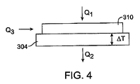
図4は、図3の装置の熱流動力学の簡易略図を示す。入力プラズマ熱流Q1は、ウェーハ310の表面上の温度T1に寄与する。加熱器308は、更なる熱流Q3をウェーハ支持体306、それによりウェーハ310にもたらす。冷却ベース302に支持体306及び断熱材304を通してシステムを出る熱流Q2は、入り熱流Q1及びQ3の両方に概ね等しい。従って:
FIG. 4 shows a simplified schematic diagram of the thermohydrodynamics of the apparatus of FIG. The input plasma
![]()
![]()
![]()
![]()
好ましくは、ベース302の温度は、入り熱流Q1がないときの概ねQ3の最大入り熱流の概ね半分の出る熱流Q2を生じさせるように設定されかつQ3の最大熱流は、Q1の最大熱流に概ね等しい:
Preferably, the temperature of

図5は、チャックの別の実施形態を示す。プラズマ加工装置用のチャックは、ウェーハ504の所望温度以下の温度を有する温度制御式ベース502を有する。断熱材料の層506は、ベース502の上に配置される。ウェーハ504を保持するために用いられるフラット支持体508は、断熱材料の層506の上に配置される。加熱器510は、フラット支持体508の下側に取り付けられる。ベース502及び断熱材料の層506は、加熱器電力線514或いは他のサービスラインが配置される穴或いはキャビティ(図示せず)を更に含む。係るサービスライン514は、加熱器、センサ、高電圧静電気クランピングのための電力線からなるのがよい。当業者は、サービスラインが先に示したものに限定されないということを認識するであろう。
FIG. 5 shows another embodiment of the chuck. The chuck for the plasma processing apparatus has a temperature
加熱器510には、断熱材506及びベース502の開口514を通して配置される電力線312によって電力が供給される。加熱器510は、少なくとも一つの抵抗加熱素子を含む。一実施形態によれば、加熱器510は、支持体508の下側に取り付けられかつ所望のパターン、例えば、対称或いは任意に成形されてもよい。(例えば、図8参照)。加熱器510は、一つ以上の平面加熱素子を含むのがよい。各加熱素子は、独立に制御される加熱ゾーン或いは領域を画成する。マルチゾーンパターンは、支持体508に対する伝導冷却に反対して作用する一つ以上の平面加熱素子を有する。
The
各加熱ゾーンと関連した少なくとも一つのセンサ516が、各加熱ゾーンの温度を測定し且つ信号をコントローラ或いはコンピュータシステム(図7参照)に送信して各個々の平面加熱素子を監視し且つ制御するのがよい。例えば、センサは、ウェーハ504から直接読み取るためにポートを通して取り付けられることができる赤外放射センサ或いは熱電対センサであるのがよい。センサ516は、支持体508内に埋設されるのがよい。
At least one sensor 516 associated with each heating zone measures the temperature of each heating zone and sends a signal to a controller or computer system (see FIG. 7) to monitor and control each individual planar heating element. Is good. For example, the sensor may be an infrared radiation sensor or a thermocouple sensor that can be mounted through a port to read directly from the
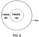
図8は、二重加熱領域:内側領域802及び外側領域804、を有する支持体508の一例を示す。各領域は、その領域自身の加熱器の組(図示せず)によって独立に加熱されるようにするのがよい。当業者は、支持体が多くの他の方法で幾何学的に画成される領域を含んでもよいということを認識するであろう。
FIG. 8 shows an example of a
半導体装置の複雑さが増すと、マルチステップ加工の使用を生じさせ、このマルチステップ加工では、単一のエッチレシピ(エッチ手段)が、エッチング加工が進行するに従ってエッチング条件を変えるために用いられる複数ステップを含む。マルチステップエッチング加工は、例えば、フォトレジストマスクが亜硝酸層をエッチするために用いられ、次いで後続する層のためのエッチングマスクとして用いられる。更に、特定層のエッチングは、エッチの実行中に変わる加工条件で高められる。特に、エッチング加工の一部分を初期温度で実行し、引き続いて、てエッチされる特定の層にとって最適なエッチング条件をもたらすようにこのレシピ内で後のステップの温度を変化させることがしばしば望ましい。 Increasing complexity of semiconductor devices results in the use of multi-step processing, where a single etch recipe (etching means) is used to change etching conditions as the etching progresses. Includes steps. Multi-step etching processes, for example, use a photoresist mask to etch the nitrite layer, and then use it as an etching mask for subsequent layers. Furthermore, the etching of specific layers is enhanced with processing conditions that change during the execution of the etch. In particular, it is often desirable to perform a portion of the etching process at an initial temperature and subsequently change the temperature of subsequent steps within this recipe to provide optimum etching conditions for the particular layer being etched.
あるエッチング加工条件は、他の加工条件よりも遥かに感温性であることが知られており、そのような場合には、エッチング加工のこの感温性であることを補償するか或いはそれを利用するために、エッチレシピ内でステップ毎にウェーハ温度を変えることができることが望ましい。例えば、相対的エッチ速度は、ある加工条件下で温度により縦方向及び横方向で異なり、この効果を、エッチング加工が進行するに従ってウェーハ温度を変えることによってエッチのそのテーパ角度を変えるために用いることができる。 Some etch processing conditions are known to be much more temperature sensitive than other processing conditions, and in such cases, this temperature sensitivity of the etching process can be compensated or reduced. For use, it is desirable to be able to change the wafer temperature from step to step within the etch recipe. For example, the relative etch rate varies longitudinally and laterally with temperature under certain processing conditions, and this effect can be used to change the taper angle of the etch by changing the wafer temperature as the etching process proceeds. Can do.
ある加工条件の下で、リアクタンスの局部濃度は、横方向エッチ速度がウェーハ全体にわたって変化するように、ウェーハ全体にわたって同様に変化する。これは、ウェーハ全体にわたってエッチされた部分の寸法形状の変化をもたらし、それは一般的に望ましくない。横方向エッチ速度の感温性を用いることにより、ウェーハ支持ゾーン温度を変えることによって径方向温度勾配を誘発することが可能であり、径方向温度勾配を誘発し、それにより局部リアクタント濃度の変化を補償してウェーハ全体にわたって一定の部分寸法形状をもたらす条件を生成するということが観測された。 Under certain processing conditions, the local concentration of reactance varies similarly across the wafer, such that the lateral etch rate varies across the wafer. This results in a change in the size and shape of the etched portion across the wafer, which is generally undesirable. By using the temperature sensitivity of the lateral etch rate, it is possible to induce a radial temperature gradient by changing the wafer support zone temperature, inducing a radial temperature gradient, thereby changing the local reactant concentration. It has been observed that a condition is created that compensates for a constant partial dimension shape across the wafer.
複数層がエッチされるような場合には、ウェーハ全体にわたって部分寸法形状を維持すること及び又は層内でテーパを生成することの必要性により、ステップ毎に基づいて並びに所与のステップ内で半径方向温度プロフィールを変えることが必要であるかもしれない。かくして、マルチゾーン温度制御式ウェーハ支持体が、ゾーンが異なる温度で作動される条件下で用いられ、且つエッチ中に加工条件を変えるマルチステップレシピが採用されるときには、異なるエッチング条件の異なる感温性を説明するか或いは利用するために温度制御式ウェーハ支持体ゾーンの温度を変えることもしばしば必要である。 In the case where multiple layers are etched, the radius is maintained on a step-by-step basis and within a given step, depending on the need to maintain partial dimensions and / or taper within the layer throughout the wafer. It may be necessary to change the directional temperature profile. Thus, when a multi-zone temperature controlled wafer support is used under conditions where the zones are operated at different temperatures, and a multi-step recipe is employed that changes the processing conditions during the etch, different temperature sensitivity of different etching conditions. It is often also necessary to change the temperature of the temperature controlled wafer support zone to account for or take advantage of the properties.
代表的なエッチングレシピの継続時間は、約20秒〜約2分であり、代表的なレシピは、レシピ内にいくつかのステップを有する。そのように、マルチステップ温度制御のために数秒内でウェーハ支持体ゾーン温度を変えることができることが必要である。興味があるほとんどの場合では、レシピ内のこれらの温度変化は、約10℃以下である。従って、毎秒約0.3℃の速度でゾーン温度を変えることができること、そして好ましくは毎秒1℃以上の速度でゾーン温度を変えることができるのが望ましい。 The duration of a typical etching recipe is about 20 seconds to about 2 minutes, and a typical recipe has several steps within the recipe. As such, it is necessary to be able to change the wafer support zone temperature within seconds for multi-step temperature control. In most cases of interest, these temperature changes within the recipe are about 10 ° C. or less. Therefore, it is desirable to be able to change the zone temperature at a rate of about 0.3 ° C. per second, and preferably to be able to change the zone temperature at a rate of 1 ° C. or more per second.
図3で説明した埋込み式加熱器を有するセラミックESCの場合について、高速ESCについての基本設計基準は、セラミックESCの熱質量が小さいこと及び加熱器電力密度が大きいことである。ESCの下の温度層の熱抵抗が比較的低い熱伝導率を有することも望ましい。かくして、ESCの厚み、加熱器電力密度、及び熱抵抗は、約毎秒1℃以上の温度変化を許容するように選択される。 In the case of a ceramic ESC having an embedded heater as described in FIG. 3, the basic design criteria for high speed ESC are a low thermal mass of the ceramic ESC and a high heater power density. It is also desirable that the thermal resistance of the temperature layer under the ESC has a relatively low thermal conductivity. Thus, the thickness of the ESC, the heater power density, and the thermal resistance are selected to allow temperature changes of about 1 ° C. or more per second.
図6は、エッチング加工中にフラット支持体の各領域の温度を空間的且つ時間的に制御することによって上記解決法を実施するフロー図を示す。特に、図6は、エッチング加工中にウェーハを加工するための方法も示す。ステップ602で、ベースが設けられる。ベースは、加工されるウェーハの温度以下である一定の温度に維持される。先に説明したように、断熱材料の層がベースの上に取り付けられる。ステップ604で、ウェーハは、異なる空間領域を含むフラット支持体の上面に保持される。先に説明したように、フラット支持体は、断熱材料の層の上に取り付けられる。ステップ606で、上記フラット支持体の各空間領域は、フラット支持体の下側に取り付けられるか或いはフラット支持体内に埋設される少なくとも一つの加熱器により初期温度まで独立に加熱される。各々の領域の初期温度は、互いに異なるようにしてもよい。ステップ608で、エッチング加工中のフラット支持体の少なくとも一つの空間領域の温度は、少なくと毎秒1℃の速度で別の温度に変えられる。各々の領域についての最終温度は、互いに異なるようにしてもよい。
FIG. 6 shows a flow diagram implementing the above solution by spatially and temporally controlling the temperature of each region of the flat support during the etching process. In particular, FIG. 6 also shows a method for processing a wafer during an etching process. At
別の実施形態によれば、各々の空間領域の温度を、各々の空間領域の内側に配置されたセンサで更に監視してもよい。センサによって生成された信号を、加熱器に供給される電力を変えることによって各々の空間領域の温度を調整するために用いてもよい。 According to another embodiment, the temperature of each spatial region may be further monitored with a sensor located inside each spatial region. The signal generated by the sensor may be used to adjust the temperature of each spatial region by changing the power supplied to the heater.
図7は、本発明の一実施形態によるチャックの温度を制御するためのシステムの略図である。ユーザ702がコンピュータ704への一組のパラメータを定義してもよい。係る一組のパラメータは、例えば、チャックの第1のゾーンの所望の温度、チャックの第2のゾーンの所望の温度であるのがよい。当業者は、チャックが一つ以上のゾーンを有してもよいということを認識するであろう。コンピュータ704は、記憶部品706と通信し、該記憶部品706は、図6のアルゴリズム、コンピュータ704の入力及び出力を記憶する。第1の組のセンサ708がチャックの第1のゾーンを測定する。第2の組のセンサ710がチャックの第2のゾーンを測定する。第1の組のセンサ708の温度測定に基づいて、コンピュータ704は、第1の組の加熱素子712に制御を送ってチャックの第1のゾーンの温度を調整する。第2の組のセンサ710の温度測定に基づいて、コンピュータ704は、第2の組の加熱素子714に制御を送ってチャックの第2のゾーンの温度を調整する。
FIG. 7 is a schematic diagram of a system for controlling the temperature of a chuck according to an embodiment of the present invention.
静電気チャックのウェーハの温度プロフィールを制御するためのこれらの一般化した方法は、誘導結合プラズマ(ICP)加工装置のアプリケーションに適するだけでなく、他のシステムアプリケーション、特にウェーハに対して低プラズマパワーフラックスを必要とするアプリケーションにも適する。この技法は、熱勾配緩和を生じさせる必要性が在る他のアプリケーションに適用してもよい。 These generalized methods for controlling the temperature profile of an electrostatic chuck wafer are not only suitable for inductively coupled plasma (ICP) processing equipment applications, but also have low plasma power flux for other system applications, especially wafers. Suitable for applications that require This technique may be applied to other applications where there is a need to cause thermal gradient relaxation.
この発明の実施形態及びアプリケーションを示し且つ説明したが、ここに示された発明の概念から逸脱することなく上記したものよりもさらに多くの変更が可能であるということは、この開示の利益を有する当業者に明らかであろう。従って、本発明は、添付した特許請求の範囲の精神以外では限定されるものではない。 While embodiments and applications of the present invention have been shown and described, it is within the benefit of this disclosure that many more modifications than those described above are possible without departing from the inventive concepts presented herein. It will be apparent to those skilled in the art. Accordingly, the invention is not limited except as by the spirit of the appended claims.
この明細書に援用されかつその一部を構成する添付図面は、本発明の一つ以上の実施形態を示し、詳細の説明と一緒に、本発明の原理及び実施例を説明する役割をする。 The accompanying drawings, which are incorporated in and constitute a part of this specification, illustrate one or more embodiments of the invention and, together with the detailed description, serve to explain the principles and examples of the invention.
302 温度制御式ベース
304 断熱材
306 支持体
308 加熱器
309 センサ
310 ウェーハ
312 熱導体
314 サービスライン
302
Claims (56)
加工物の所望温度以下の温度を有する温度制御式ベースと、
上記ベースの上に配置された断熱材料の層と、
上記断熱材料の層の上に配置され、上記加工物を保持するための平坦支持体と、
上記平坦支持体の下側に結合され、上記平坦支持体の複数の加熱領域に対応する複数の平面加熱素子を含む加熱器と、を含み、
上記加熱器は、毎秒少なくとも1℃の温度割合変化を有する、上記チャック。 A chuck for a plasma processing apparatus,
A temperature controlled base having a temperature below the desired temperature of the workpiece;
A layer of thermal insulation material disposed on the base;
A flat support disposed on the layer of thermal insulation material to hold the workpiece;
A heater coupled to the underside of the flat support and including a plurality of planar heating elements corresponding to a plurality of heating regions of the flat support;
The chuck, wherein the heater has a temperature rate change of at least 1 ° C. per second.
加工物の所望温度以下の温度を有する温度制御式ベースと、
上記ベースの上に配置された断熱材料の層と、
上記断熱材料の層の上に配置され、上記加工物を保持するための平坦支持体と、
上記平坦支持体内に埋め込まれ、上記平坦支持体の複数の加熱領域に対応する複数の平面加熱素子を含む加熱器と、を含み、
上記加熱器及び上記平坦支持体の温度は、毎秒少なくとも1℃の変化が可能であるように構成される、上記チャック。 A chuck for a plasma processing apparatus,
A temperature controlled base having a temperature below the desired temperature of the workpiece;
A layer of thermal insulation material disposed on the base;
A flat support disposed on the layer of thermal insulation material to hold the workpiece;
A heater embedded in the flat support and including a plurality of planar heating elements corresponding to a plurality of heating regions of the flat support,
The chuck, wherein the heater and the temperature of the flat support are configured to be capable of changing at least 1 ° C. per second.
加工物の温度以下である一定温度に維持され、上に取り付けられた断熱材料の層を有する、ベースを用意し、
上記加工物を複数の空間領域を有し、上記断熱材料の層の上に取り付けられた、平坦支持体の上面に保持し、
上記平坦支持体の各空間領域を上記平坦支持体の下側に取り付けられた複数の加熱器で独立に加熱し、
エッチング加工中上記平坦支持体の少なくとも一つの空間領域の温度を毎秒少なくとも1℃の割合変える、上記方法。 A method for controlling the temperature of a space across a workpiece,
Providing a base, having a layer of thermal insulation material mounted thereon, maintained at a constant temperature that is below the temperature of the workpiece;
Holding the work piece on the top surface of a flat support having a plurality of spatial regions and mounted on the layer of thermal insulation material;
Heating each space region of the flat support independently with a plurality of heaters attached to the underside of the flat support;
The method, wherein the temperature of at least one spatial region of the flat support is changed at a rate of at least 1 ° C. per second during the etching process.
加工物の温度以下である一定温度に維持され、上に取り付けられた断熱材料の層を有するベースを用意し、
複数の空間領域を有し、上記断熱材料の層の上に取り付けられた平坦支持体の上面に上記加工物を保持し、
上記平坦支持体の各空間領域を上記平坦支持体内に埋め込まれた複数の加熱器で独立に加熱し、
エッチング加工中上記平坦支持体の少なくとも一つの空間領域の温度を毎秒少なくとも1℃の割合で変える、上記方法。 A method for controlling the temperature of a space across a workpiece,
Prepare a base having a layer of thermal insulation material attached on top, maintained at a constant temperature that is below the temperature of the workpiece,
Holding the workpiece on the upper surface of a flat support having a plurality of spatial regions and mounted on the layer of thermal insulation material;
Heating each space region of the flat support independently with a plurality of heaters embedded in the flat support;
The method, wherein the temperature of at least one spatial region of the flat support is changed at a rate of at least 1 ° C. per second during the etching process.
上記加工物の温度以下である一定温度に維持され、上に取り付けられた断熱材料の層を有するベースを用意するための手段と、
複数の空間領域を有し、上記断熱材料の層の上に取り付けられた平坦支持体の上面に上記加工物を保持するための手段と、
上記平坦支持体の各空間領域を該平坦支持体の下側に取り付けられた複数の加熱器で独立に加熱するための手段と、
エッチング加工中上記平坦支持体の少なくとも一つの空間領域の温度を毎秒少なくとも1℃の割合で変えるための手段と、を含む上記装置。 A device for controlling the temperature of the space across the workpiece,
Means for providing a base that is maintained at a constant temperature that is less than or equal to the temperature of the workpiece and that has a layer of thermal insulating material mounted thereon;
Means for holding the workpiece on the upper surface of a flat support having a plurality of spatial regions and mounted on the layer of thermal insulation material;
Means for independently heating each spatial region of the flat support with a plurality of heaters attached to the underside of the flat support;
Means for changing the temperature of at least one spatial region of the flat support at a rate of at least 1 ° C per second during the etching process.
上記加工物の温度以下である一定温度に維持され、上に取り付けられた断熱材料の層を有するベースを用意するための手段と、
複数の空間領域を有し、上記断熱材料の層の上に取り付けられた平坦支持体の上面に上記加工物を保持するための手段と、
上記平坦支持体の各空間領域を該平坦支持体内に埋め込まれた複数の加熱器で独立に加熱するための手段と、
エッチング加工中上記平坦支持体の少なくとも一つの空間領域の温度を毎秒少なくとも1℃の割合で変えるための手段と、を含む上記装置。 A device for controlling the temperature of the space across the workpiece,
Means for providing a base that is maintained at a constant temperature that is less than or equal to the temperature of the workpiece and that has a layer of thermal insulating material mounted thereon;
Means for holding the workpiece on the upper surface of a flat support having a plurality of spatial regions and mounted on the layer of thermal insulation material;
Means for independently heating each spatial region of the flat support with a plurality of heaters embedded in the flat support;
Means for changing the temperature of at least one spatial region of the flat support at a rate of at least 1 ° C per second during the etching process.
少なくとも第1の部分及び第2の部分を含む、少なくとも二つの部分に、少なくとも一つの横方向サーマルブレークによって熱的に分離された単一ピースのベース素子と、
上記第1の部分及び上記第2の部分の上に配置されたウェーハ支持体素子と、を含み、
上記ウェーハ支持体は、上記ベースの上記第1の部分の上に配置された上記加工物の温度に影響を及ぼすように構成される少なくとも第1の熱素子と、上記ベースの上記第2の部分の上に配置された上記加工物の温度に影響を及ぼす第2の熱素子とを含む、チャック組立体。 A workpiece chuck assembly for a plasma processing apparatus,
A single piece base element thermally separated into at least two parts, including at least a first part and a second part, by at least one lateral thermal break; and
A wafer support element disposed on the first portion and the second portion, and
The wafer support includes at least a first thermal element configured to affect the temperature of the workpiece disposed on the first portion of the base, and the second portion of the base. And a second thermal element that affects the temperature of the workpiece disposed on the chuck assembly.
少なくとも内側円盤形部分と外側円盤形部分とを含む、少なくとも2つの円盤形部分に、垂直に配置された横方向サーマルブレークによって熱的に分離された単一ピースベース素子と、
上記内側及び外側円盤形部分の上に配置されたウェーハ支持体素子と、を含み、
上記ウェーハ支持体素子は、上記内側円盤形部分の上に配置された上記加工物の温度に影響を及ぼすように構成された少なくとも第1の熱素子と、上記外側円盤形部分の上に配置された上記加工物の温度に影響を及ぼす第2の熱素子とを含む、チャック組立体。 A workpiece chuck assembly for a plasma processing apparatus,
A single piece base element thermally separated by a transverse thermal break vertically disposed in at least two disk-shaped portions, including at least an inner disk-shaped portion and an outer disk-shaped portion;
Wafer support elements disposed on the inner and outer disk-shaped portions, and
The wafer support element is disposed on the outer disk-shaped portion and at least a first thermal element configured to affect the temperature of the workpiece disposed on the inner disk-shaped portion. And a second thermal element that affects the temperature of the workpiece.
Applications Claiming Priority (2)
| Application Number | Priority Date | Filing Date | Title |
|---|---|---|---|
| US11/004,179 US20050211385A1 (en) | 2001-04-30 | 2004-12-02 | Method and apparatus for controlling spatial temperature distribution |
| PCT/US2005/043801 WO2006068805A1 (en) | 2004-12-02 | 2005-12-01 | Method and apparatus for controlling spatial temperature distribution |
Related Child Applications (1)
| Application Number | Title | Priority Date | Filing Date |
|---|---|---|---|
| JP2011176261A Division JP2011244011A (en) | 2004-12-02 | 2011-08-11 | Method and apparatus for controlling spatial temperature distribution |
Publications (2)
| Publication Number | Publication Date |
|---|---|
| JP2008522446A true JP2008522446A (en) | 2008-06-26 |
| JP2008522446A5 JP2008522446A5 (en) | 2012-08-09 |
Family
ID=36295018
Family Applications (3)
| Application Number | Title | Priority Date | Filing Date |
|---|---|---|---|
| JP2007544574A Pending JP2008522446A (en) | 2004-12-02 | 2005-12-01 | Method and apparatus for controlling spatial temperature distribution |
| JP2011176261A Pending JP2011244011A (en) | 2004-12-02 | 2011-08-11 | Method and apparatus for controlling spatial temperature distribution |
| JP2014055288A Pending JP2014146822A (en) | 2004-12-02 | 2014-03-18 | Method and apparatus for controlling spatial temperature distribution |
Family Applications After (2)
| Application Number | Title | Priority Date | Filing Date |
|---|---|---|---|
| JP2011176261A Pending JP2011244011A (en) | 2004-12-02 | 2011-08-11 | Method and apparatus for controlling spatial temperature distribution |
| JP2014055288A Pending JP2014146822A (en) | 2004-12-02 | 2014-03-18 | Method and apparatus for controlling spatial temperature distribution |
Country Status (7)
| Country | Link |
|---|---|
| US (3) | US20050211385A1 (en) |
| JP (3) | JP2008522446A (en) |
| KR (1) | KR101109440B1 (en) |
| CN (2) | CN102122607B (en) |
| SG (3) | SG10201408008QA (en) |
| TW (1) | TWI481297B (en) |
| WO (1) | WO2006068805A1 (en) |
Cited By (10)
| Publication number | Priority date | Publication date | Assignee | Title |
|---|---|---|---|---|
| JP2008085329A (en) * | 2006-09-25 | 2008-04-10 | Tokyo Electron Ltd | Temperature controlled substrate holder having erosion resistant insulating layer used for substrate processing system |
| JP2010118551A (en) * | 2008-11-13 | 2010-05-27 | Tokyo Electron Ltd | Electrostatic chuck and substrate processing apparatus |
| JP2011049425A (en) * | 2009-08-28 | 2011-03-10 | Ngk Spark Plug Co Ltd | Component for semiconductor manufacturing device |
| JP2011258953A (en) * | 2010-06-07 | 2011-12-22 | Lam Research Corporation | Plasma processing chamber component having adaptive thermal conductor |
| JP2012508991A (en) * | 2008-11-12 | 2012-04-12 | ラム リサーチ コーポレーション | Improved substrate temperature control by liquid controlled multi-region substrate support |
| WO2012128348A1 (en) * | 2011-03-23 | 2012-09-27 | 住友大阪セメント株式会社 | Electrostatic chuck device |
| JP2013149977A (en) * | 2006-09-25 | 2013-08-01 | Tokyo Electron Ltd | Temperature controlled substrate holder with non-uniform insulation layer for substrate processing system |
| JP2015162586A (en) * | 2014-02-27 | 2015-09-07 | 東京エレクトロン株式会社 | Electrostatic chuck and temperature control method of electrostatic chuck |
| JP2016534556A (en) * | 2013-08-06 | 2016-11-04 | アプライド マテリアルズ インコーポレイテッドApplied Materials,Incorporated | Multi-zone substrate support heated locally |
| JP2016189425A (en) * | 2015-03-30 | 2016-11-04 | 日本特殊陶業株式会社 | Ceramic heater and control method therefor, electrostatic chuck and control method therefor |
Families Citing this family (64)
| Publication number | Priority date | Publication date | Assignee | Title |
|---|---|---|---|---|
| US20050211385A1 (en) | 2001-04-30 | 2005-09-29 | Lam Research Corporation, A Delaware Corporation | Method and apparatus for controlling spatial temperature distribution |
| US8038796B2 (en) | 2004-12-30 | 2011-10-18 | Lam Research Corporation | Apparatus for spatial and temporal control of temperature on a substrate |
| US7525787B2 (en) * | 2005-09-30 | 2009-04-28 | Lam Research Corporation | Electrostatic chuck assembly with dielectric material and/or cavity having varying thickness, profile and/or shape, method of use and apparatus incorporating same |
| TW200802553A (en) * | 2006-05-17 | 2008-01-01 | Eagle Ind Co Ltd | Heating apparatus |
| US7501605B2 (en) * | 2006-08-29 | 2009-03-10 | Lam Research Corporation | Method of tuning thermal conductivity of electrostatic chuck support assembly |
| KR101508026B1 (en) * | 2007-10-31 | 2015-04-08 | 램 리써치 코포레이션 | Temperature control module using gas pressure to control thermal conductance between liquid coolant and component body |
| JP5222442B2 (en) * | 2008-02-06 | 2013-06-26 | 東京エレクトロン株式会社 | Substrate mounting table, substrate processing apparatus, and temperature control method for substrate to be processed |
| US8133819B2 (en) * | 2008-02-21 | 2012-03-13 | Applied Materials, Inc. | Plasma etching carbonaceous layers with sulfur-based etchants |
| KR20100037765A (en) * | 2008-10-02 | 2010-04-12 | 삼성전자주식회사 | Plasma generating device |
| KR101691044B1 (en) * | 2009-02-04 | 2016-12-29 | 맷슨 테크놀로지, 인크. | Electrostatic chuck system and process for radially tuning the temperature profile across the surface of a substrate |
| US8637794B2 (en) | 2009-10-21 | 2014-01-28 | Lam Research Corporation | Heating plate with planar heating zones for semiconductor processing |
| KR101841378B1 (en) | 2009-12-15 | 2018-03-22 | 램 리써치 코포레이션 | Adjusting substrate temperature to improve cd uniformity |
| US8410393B2 (en) | 2010-05-24 | 2013-04-02 | Lam Research Corporation | Apparatus and method for temperature control of a semiconductor substrate support |
| US8580693B2 (en) * | 2010-08-27 | 2013-11-12 | Applied Materials, Inc. | Temperature enhanced electrostatic chucking in plasma processing apparatus |
| US8822876B2 (en) * | 2010-10-15 | 2014-09-02 | Applied Materials, Inc. | Multi-zoned plasma processing electrostatic chuck with improved temperature uniformity |
| US8791392B2 (en) | 2010-10-22 | 2014-07-29 | Lam Research Corporation | Methods of fault detection for multiplexed heater array |
| US8546732B2 (en) | 2010-11-10 | 2013-10-01 | Lam Research Corporation | Heating plate with planar heater zones for semiconductor processing |
| JP4980461B1 (en) * | 2010-12-24 | 2012-07-18 | 三井造船株式会社 | Induction heating device |
| JP6021006B2 (en) * | 2010-12-27 | 2016-11-02 | 株式会社クリエイティブテクノロジー | Work heating device and work processing device |
| WO2013033348A1 (en) * | 2011-08-30 | 2013-03-07 | Watlow Electric Manufacturing Company | System and method for controlling a thermal array |
| US10388493B2 (en) | 2011-09-16 | 2019-08-20 | Lam Research Corporation | Component of a substrate support assembly producing localized magnetic fields |
| US8624168B2 (en) | 2011-09-20 | 2014-01-07 | Lam Research Corporation | Heating plate with diode planar heater zones for semiconductor processing |
| CN103123906A (en) * | 2011-11-18 | 2013-05-29 | 中芯国际集成电路制造(北京)有限公司 | Reaction device for processing wafer, electrostatic chuck and wafer temperature control method |
| CN103137517B (en) * | 2011-11-25 | 2016-08-03 | 中芯国际集成电路制造(北京)有限公司 | For processing the reaction unit of wafer, electrostatic chuck and wafer temperature control method |
| JP6017781B2 (en) * | 2011-12-07 | 2016-11-02 | 新光電気工業株式会社 | Substrate temperature adjustment fixing device and manufacturing method thereof |
| NL2009858A (en) * | 2011-12-27 | 2013-07-01 | Asml Netherlands Bv | Substrate holder, lithographic apparatus, and device manufacturing method. |
| US9324589B2 (en) | 2012-02-28 | 2016-04-26 | Lam Research Corporation | Multiplexed heater array using AC drive for semiconductor processing |
| US8809747B2 (en) | 2012-04-13 | 2014-08-19 | Lam Research Corporation | Current peak spreading schemes for multiplexed heated array |
| US10049948B2 (en) * | 2012-11-30 | 2018-08-14 | Lam Research Corporation | Power switching system for ESC with array of thermal control elements |
| US9538583B2 (en) * | 2013-01-16 | 2017-01-03 | Applied Materials, Inc. | Substrate support with switchable multizone heater |
| US20140251214A1 (en) * | 2013-03-06 | 2014-09-11 | Applied Materials, Inc. | Heated substrate support with flatness control |
| US20140356985A1 (en) | 2013-06-03 | 2014-12-04 | Lam Research Corporation | Temperature controlled substrate support assembly |
| JP6159172B2 (en) * | 2013-06-26 | 2017-07-05 | 東京エレクトロン株式会社 | Temperature control method and plasma processing apparatus |
| US9541846B2 (en) * | 2013-09-06 | 2017-01-10 | Taiwan Semiconductor Manufacturing Co., Ltd. | Homogeneous thermal equalization with active device |
| US9417138B2 (en) * | 2013-09-10 | 2016-08-16 | Varian Semiconductor Equipment Associates, Inc. | Gas coupled probe for substrate temperature measurement |
| KR101458864B1 (en) * | 2013-09-30 | 2014-11-07 | (주)엘케이솔루션 | Electostatic chuck |
| CN104600000A (en) * | 2013-10-30 | 2015-05-06 | 沈阳芯源微电子设备有限公司 | Surrounding absorbing roasting structure of base plate |
| CN104637838B (en) * | 2013-11-15 | 2018-06-26 | 中微半导体设备(上海)有限公司 | A kind of semiconductor processing device |
| US10006717B2 (en) | 2014-03-07 | 2018-06-26 | Taiwan Semiconductor Manufacturing Company, Ltd. | Adaptive baking system and method of using the same |
| US9543171B2 (en) | 2014-06-17 | 2017-01-10 | Lam Research Corporation | Auto-correction of malfunctioning thermal control element in a temperature control plate of a semiconductor substrate support assembly that includes deactivating the malfunctioning thermal control element and modifying a power level of at least one functioning thermal control element |
| JP6392612B2 (en) * | 2014-09-30 | 2018-09-19 | 日本特殊陶業株式会社 | Electrostatic chuck |
| KR20160054153A (en) * | 2014-11-05 | 2016-05-16 | 삼성전자주식회사 | Laser annealing apparatus |
| JP6806704B2 (en) | 2015-05-22 | 2021-01-06 | アプライド マテリアルズ インコーポレイテッドApplied Materials,Incorporated | Multi-zone electrostatic chuck adjustable in azimuth direction |
| WO2017003646A1 (en) * | 2015-06-29 | 2017-01-05 | Varian Semiconductor Equipment Associates, Inc. | Thermal shield for electrostatic chuck |
| TWI757242B (en) * | 2015-08-06 | 2022-03-11 | 美商應用材料股份有限公司 | Thermal management systems and methods for wafer processing systems |
| US10690414B2 (en) * | 2015-12-11 | 2020-06-23 | Lam Research Corporation | Multi-plane heater for semiconductor substrate support |
| KR20180114088A (en) * | 2016-02-08 | 2018-10-17 | 와틀로 일렉트릭 매뉴팩츄어링 컴파니 | Temperature measurement system for rotatable wafer support assembly |
| CN107331595B (en) * | 2016-04-29 | 2019-08-13 | 中微半导体设备(上海)股份有限公司 | For plasma treatment appts and its temprature control method and calibration method |
| US11069553B2 (en) * | 2016-07-07 | 2021-07-20 | Lam Research Corporation | Electrostatic chuck with features for preventing electrical arcing and light-up and improving process uniformity |
| JP2018063974A (en) * | 2016-10-11 | 2018-04-19 | 東京エレクトロン株式会社 | Temperature controller, temperature control method, and placement table |
| CN108062124B (en) * | 2016-11-08 | 2020-04-07 | 中微半导体设备(上海)股份有限公司 | Temperature control wafer mounting table and temperature control method thereof |
| US10910195B2 (en) | 2017-01-05 | 2021-02-02 | Lam Research Corporation | Substrate support with improved process uniformity |
| US11062886B2 (en) * | 2017-11-28 | 2021-07-13 | Taiwan Semiconductor Manufacturing Co., Ltd. | Apparatus and method for controlling wafer uniformity |
| KR102091515B1 (en) * | 2018-02-22 | 2020-03-20 | 주식회사 에프에스티 | Electrostatic chuck and device of controlling a semiconductor processing apparatus |
| KR20200023988A (en) | 2018-08-27 | 2020-03-06 | 삼성전자주식회사 | Electro-static chuck and wafer etching device comprising the same |
| KR102225682B1 (en) * | 2018-09-28 | 2021-03-12 | 세메스 주식회사 | Heat treating method of substrate |
| CN109473381A (en) * | 2018-10-31 | 2019-03-15 | 上海华力微电子有限公司 | Wet etching cleaning device and method |
| KR102211817B1 (en) * | 2018-12-14 | 2021-02-05 | 세메스 주식회사 | Liquid supply unit and substrate processing apparatus |
| DE102019207772A1 (en) * | 2019-05-28 | 2020-12-03 | Siltronic Ag | Method for depositing an epitaxial layer on a front side of a semiconductor wafer and device for carrying out the method |
| CN110600419A (en) * | 2019-09-20 | 2019-12-20 | 上海华力微电子有限公司 | Electrostatic chuck and using method thereof |
| CN110707035A (en) * | 2019-10-16 | 2020-01-17 | 北京北方华创微电子装备有限公司 | Electrostatic chuck, semiconductor processing chamber and apparatus |
| CN110752171B (en) * | 2019-11-01 | 2022-07-29 | 长江存储科技有限责任公司 | Device and method for adjusting wafer curvature |
| JP7330078B2 (en) * | 2019-11-25 | 2023-08-21 | 東京エレクトロン株式会社 | Etching method and etching apparatus |
| US20220223425A1 (en) * | 2021-01-08 | 2022-07-14 | Taiwan Semiconductor Manufacturing Co., Ltd. | By-site-compensated etch back for local planarization/topography adjustment |
Citations (6)
| Publication number | Priority date | Publication date | Assignee | Title |
|---|---|---|---|---|
| JPH10144655A (en) * | 1996-11-06 | 1998-05-29 | Sony Corp | Method and apparatus for dry etching |
| JPH11243077A (en) * | 1997-12-26 | 1999-09-07 | Hitachi Ltd | Method and device for plasma treatment |
| JP2000332089A (en) * | 1999-05-18 | 2000-11-30 | Toshiba Ceramics Co Ltd | Electrostatic chuck for heating and holding wafer |
| JP2002057207A (en) * | 2000-01-20 | 2002-02-22 | Sumitomo Electric Ind Ltd | Wafer holder for semiconductor-manufacturing apparatus, manufacturing method of the same and the semiconductor-manufacturing apparatus |
| JP2002076103A (en) * | 2000-08-23 | 2002-03-15 | Hitachi Ltd | Method and apparatus for controlling temperature of sample stage, and method and apparatus for processing sample |
| JP2002252271A (en) * | 2001-02-26 | 2002-09-06 | Anelva Corp | Substrate holding device for substrate processing apparatus |
Family Cites Families (74)
| Publication number | Priority date | Publication date | Assignee | Title |
|---|---|---|---|---|
| US2152126A (en) * | 1936-10-02 | 1939-03-28 | John Wentworth | Heating device |
| US3634740A (en) * | 1970-04-20 | 1972-01-11 | Addressograph Multigraph | Electrostatic holddown |
| US4361749A (en) * | 1980-02-04 | 1982-11-30 | Western Electric Co., Inc. | Uniformly cooled plasma etching electrode |
| US4518848A (en) * | 1981-05-15 | 1985-05-21 | Gca Corporation | Apparatus for baking resist on semiconductor wafers |
| JPS6129127A (en) | 1984-07-20 | 1986-02-10 | Hitachi Hokkai Semiconductor Kk | Treating device |
| JPH079887B2 (en) | 1985-05-22 | 1995-02-01 | 三洋電機株式会社 | Liquid phase epitaxial growth method |
| JPH0310443U (en) | 1989-06-19 | 1991-01-31 | ||
| US5059770A (en) * | 1989-09-19 | 1991-10-22 | Watkins-Johnson Company | Multi-zone planar heater assembly and method of operation |
| US5192849A (en) * | 1990-08-10 | 1993-03-09 | Texas Instruments Incorporated | Multipurpose low-thermal-mass chuck for semiconductor processing equipment |
| JP3238925B2 (en) * | 1990-11-17 | 2001-12-17 | 株式会社東芝 | Electrostatic chuck |
| JPH04196528A (en) * | 1990-11-28 | 1992-07-16 | Toshiba Corp | Magnetron etching system |
| JPH04360526A (en) | 1991-06-07 | 1992-12-14 | Nec Corp | Fine pattern forming method |
| US5580607A (en) * | 1991-07-26 | 1996-12-03 | Tokyo Electron Limited | Coating apparatus and method |
| US5294778A (en) * | 1991-09-11 | 1994-03-15 | Lam Research Corporation | CVD platen heater system utilizing concentric electric heating elements |
| US5376213A (en) * | 1992-07-28 | 1994-12-27 | Tokyo Electron Limited | Plasma processing apparatus |
| JP2906006B2 (en) * | 1992-10-15 | 1999-06-14 | 東京エレクトロン株式会社 | Processing method and apparatus |
| US5413360A (en) * | 1992-12-01 | 1995-05-09 | Kyocera Corporation | Electrostatic chuck |
| US5460684A (en) * | 1992-12-04 | 1995-10-24 | Tokyo Electron Limited | Stage having electrostatic chuck and plasma processing apparatus using same |
| JPH06283594A (en) | 1993-03-24 | 1994-10-07 | Tokyo Electron Ltd | Electrostatic chuck |
| JPH06295888A (en) | 1993-04-09 | 1994-10-21 | Sony Corp | Fabrication of semiconductor device |
| US5591269A (en) * | 1993-06-24 | 1997-01-07 | Tokyo Electron Limited | Vacuum processing apparatus |
| TW277139B (en) * | 1993-09-16 | 1996-06-01 | Hitachi Seisakusyo Kk | |
| US5529657A (en) * | 1993-10-04 | 1996-06-25 | Tokyo Electron Limited | Plasma processing apparatus |
| JPH07201822A (en) | 1993-12-28 | 1995-08-04 | Hiroshima Nippon Denki Kk | Dry etching device |
| JP2647799B2 (en) * | 1994-02-04 | 1997-08-27 | 日本碍子株式会社 | Ceramic heater and manufacturing method thereof |
| JP3247249B2 (en) | 1994-05-12 | 2002-01-15 | 東京エレクトロン株式会社 | Plasma processing equipment |
| JP3208029B2 (en) * | 1994-11-22 | 2001-09-10 | 株式会社巴川製紙所 | Electrostatic chuck device and manufacturing method thereof |
| JPH08191059A (en) * | 1995-01-09 | 1996-07-23 | Hitachi Ltd | Plasma treating device |
| US5671116A (en) | 1995-03-10 | 1997-09-23 | Lam Research Corporation | Multilayered electrostatic chuck and method of manufacture thereof |
| JP3548634B2 (en) | 1995-07-14 | 2004-07-28 | 東京エレクトロン株式会社 | Film forming apparatus and method for removing deposited film in the apparatus |
| US5854468A (en) * | 1996-01-25 | 1998-12-29 | Brooks Automation, Inc. | Substrate heating apparatus with cantilevered lifting arm |
| JPH09260474A (en) | 1996-03-22 | 1997-10-03 | Sony Corp | Electrostatic chuck and wafer stage |
| JPH10256359A (en) | 1997-03-08 | 1998-09-25 | Seiichiro Miyata | Electrostatic chuck |
| DE69731740T2 (en) * | 1996-05-05 | 2005-12-15 | Tateho Chemical Industries Co., Ltd., Akou | ELECTRIC HEATING ELEMENT AND THIS VERSION OF TENSIONING DEVICE |
| JP3537269B2 (en) * | 1996-05-21 | 2004-06-14 | アネルバ株式会社 | Multi-chamber sputtering equipment |
| JPH1014266A (en) * | 1996-06-21 | 1998-01-16 | Sony Corp | Electrostatic chucking device and wafer retention/ removal therewith/therefrom |
| WO1998005060A1 (en) * | 1996-07-31 | 1998-02-05 | The Board Of Trustees Of The Leland Stanford Junior University | Multizone bake/chill thermal cycling module |
| US5846375A (en) * | 1996-09-26 | 1998-12-08 | Micron Technology, Inc. | Area specific temperature control for electrode plates and chucks used in semiconductor processing equipment |
| US6022587A (en) * | 1997-05-13 | 2000-02-08 | Applied Materials, Inc. | Method and apparatus for improving film deposition uniformity on a substrate |
| JP3665826B2 (en) * | 1997-05-29 | 2005-06-29 | Smc株式会社 | Substrate heat treatment equipment |
| US5978202A (en) * | 1997-06-27 | 1999-11-02 | Applied Materials, Inc. | Electrostatic chuck having a thermal transfer regulator pad |
| JP3318514B2 (en) * | 1997-08-06 | 2002-08-26 | 日本碍子株式会社 | Semiconductor support device |
| EP0915499B1 (en) * | 1997-11-05 | 2011-03-23 | Tokyo Electron Limited | Semiconductor wafer holding apparatus |
| JP3400692B2 (en) | 1997-11-05 | 2003-04-28 | 東京エレクトロン株式会社 | Wafer temperature control device and wafer storage room |
| US6482747B1 (en) * | 1997-12-26 | 2002-11-19 | Hitachi, Ltd. | Plasma treatment method and plasma treatment apparatus |
| JP3477062B2 (en) * | 1997-12-26 | 2003-12-10 | 京セラ株式会社 | Wafer heating device |
| JP4013386B2 (en) * | 1998-03-02 | 2007-11-28 | 住友電気工業株式会社 | Support for manufacturing semiconductor and method for manufacturing the same |
| US6020262A (en) * | 1998-03-06 | 2000-02-01 | Siemens Aktiengesellschaft | Methods and apparatus for chemical mechanical planarization (CMP) of a semiconductor wafer |
| US6190732B1 (en) | 1998-09-03 | 2001-02-20 | Cvc Products, Inc. | Method and system for dispensing process gas for fabricating a device on a substrate |
| US6259592B1 (en) * | 1998-11-19 | 2001-07-10 | Applied Materials, Inc. | Apparatus for retaining a workpiece upon a workpiece support and method of manufacturing same |
| JP2000216140A (en) | 1999-01-20 | 2000-08-04 | Hitachi Ltd | Wafer stage and wafer treating apparatus |
| JP2001102436A (en) | 1999-05-07 | 2001-04-13 | Applied Materials Inc | Electrostatic chuck and its manufacturing method |
| US6310755B1 (en) * | 1999-05-07 | 2001-10-30 | Applied Materials, Inc. | Electrostatic chuck having gas cavity and method |
| US6705394B1 (en) * | 1999-10-29 | 2004-03-16 | Cvc Products, Inc. | Rapid cycle chuck for low-pressure processing |
| JP4209057B2 (en) * | 1999-12-01 | 2009-01-14 | 東京エレクトロン株式会社 | Ceramic heater, substrate processing apparatus and substrate processing method using the same |
| JP2001203257A (en) * | 2000-01-20 | 2001-07-27 | Sumitomo Electric Ind Ltd | Wafer holder for semiconductor manufacturing apparatus |
| JP3228924B2 (en) * | 2000-01-21 | 2001-11-12 | イビデン株式会社 | Ceramic heater for semiconductor manufacturing and inspection equipment |
| US6472643B1 (en) * | 2000-03-07 | 2002-10-29 | Silicon Valley Group, Inc. | Substrate thermal management system |
| JP2001313155A (en) * | 2000-04-28 | 2001-11-09 | Kyocera Corp | Disc heater and wafer treatment device |
| JP2002009140A (en) | 2000-06-22 | 2002-01-11 | Mitsubishi Electric Corp | Electrostatic chuck apparatus |
| JP2002110647A (en) | 2000-09-29 | 2002-04-12 | Hitachi Ltd | Manufacturing method of semiconductor integrated circuit device |
| JP2002231804A (en) | 2001-01-31 | 2002-08-16 | Toshiba Corp | Semiconductor device and its manufacturing method |
| JP2002313901A (en) | 2001-04-12 | 2002-10-25 | Komatsu Ltd | Electrostatic chuck |
| US6847014B1 (en) * | 2001-04-30 | 2005-01-25 | Lam Research Corporation | Method and apparatus for controlling the spatial temperature distribution across the surface of a workpiece support |
| JP4549022B2 (en) * | 2001-04-30 | 2010-09-22 | ラム リサーチ コーポレイション | Method and apparatus for controlling spatial temperature distribution across the surface of a workpiece support |
| US20050211385A1 (en) | 2001-04-30 | 2005-09-29 | Lam Research Corporation, A Delaware Corporation | Method and apparatus for controlling spatial temperature distribution |
| JP2002359281A (en) | 2001-06-01 | 2002-12-13 | Ngk Spark Plug Co Ltd | Ceramic heater and manufacturing method therefor |
| JP2003060016A (en) | 2001-07-31 | 2003-02-28 | Applied Materials Inc | Current introducing terminal and semiconductor manufacturing apparatus |
| US6538872B1 (en) * | 2001-11-05 | 2003-03-25 | Applied Materials, Inc. | Electrostatic chuck having heater and method |
| US6664738B2 (en) | 2002-02-27 | 2003-12-16 | Hitachi, Ltd. | Plasma processing apparatus |
| US6921724B2 (en) * | 2002-04-02 | 2005-07-26 | Lam Research Corporation | Variable temperature processes for tunable electrostatic chuck |
| US20040163601A1 (en) | 2003-02-26 | 2004-08-26 | Masanori Kadotani | Plasma processing apparatus |
| US6770852B1 (en) * | 2003-02-27 | 2004-08-03 | Lam Research Corporation | Critical dimension variation compensation across a wafer by means of local wafer temperature control |
| KR101214520B1 (en) * | 2005-04-26 | 2012-12-24 | 가부시키가이샤 한도오따이 에네루기 켄큐쇼 | Light emitting device and method for driving thereof |
-
2004
- 2004-12-02 US US11/004,179 patent/US20050211385A1/en not_active Abandoned
-
2005
- 2005-12-01 SG SG10201408008QA patent/SG10201408008QA/en unknown
- 2005-12-01 KR KR1020077014977A patent/KR101109440B1/en active IP Right Grant
- 2005-12-01 WO PCT/US2005/043801 patent/WO2006068805A1/en active Application Filing
- 2005-12-01 SG SG10201609601XA patent/SG10201609601XA/en unknown
- 2005-12-01 CN CN2010106228155A patent/CN102122607B/en active Active
- 2005-12-01 SG SG200907998-9A patent/SG158101A1/en unknown
- 2005-12-01 JP JP2007544574A patent/JP2008522446A/en active Pending
- 2005-12-01 CN CNA2005800472891A patent/CN101111934A/en active Pending
- 2005-12-02 TW TW094142661A patent/TWI481297B/en active
-
2009
- 2009-05-06 US US12/436,443 patent/US8963052B2/en active Active
-
2011
- 2011-08-11 JP JP2011176261A patent/JP2011244011A/en active Pending
-
2014
- 2014-03-18 JP JP2014055288A patent/JP2014146822A/en active Pending
-
2015
- 2015-01-12 US US14/594,648 patent/US9824904B2/en not_active Expired - Lifetime
Patent Citations (6)
| Publication number | Priority date | Publication date | Assignee | Title |
|---|---|---|---|---|
| JPH10144655A (en) * | 1996-11-06 | 1998-05-29 | Sony Corp | Method and apparatus for dry etching |
| JPH11243077A (en) * | 1997-12-26 | 1999-09-07 | Hitachi Ltd | Method and device for plasma treatment |
| JP2000332089A (en) * | 1999-05-18 | 2000-11-30 | Toshiba Ceramics Co Ltd | Electrostatic chuck for heating and holding wafer |
| JP2002057207A (en) * | 2000-01-20 | 2002-02-22 | Sumitomo Electric Ind Ltd | Wafer holder for semiconductor-manufacturing apparatus, manufacturing method of the same and the semiconductor-manufacturing apparatus |
| JP2002076103A (en) * | 2000-08-23 | 2002-03-15 | Hitachi Ltd | Method and apparatus for controlling temperature of sample stage, and method and apparatus for processing sample |
| JP2002252271A (en) * | 2001-02-26 | 2002-09-06 | Anelva Corp | Substrate holding device for substrate processing apparatus |
Cited By (11)
| Publication number | Priority date | Publication date | Assignee | Title |
|---|---|---|---|---|
| JP2008085329A (en) * | 2006-09-25 | 2008-04-10 | Tokyo Electron Ltd | Temperature controlled substrate holder having erosion resistant insulating layer used for substrate processing system |
| JP2013149977A (en) * | 2006-09-25 | 2013-08-01 | Tokyo Electron Ltd | Temperature controlled substrate holder with non-uniform insulation layer for substrate processing system |
| JP2012508991A (en) * | 2008-11-12 | 2012-04-12 | ラム リサーチ コーポレーション | Improved substrate temperature control by liquid controlled multi-region substrate support |
| JP2010118551A (en) * | 2008-11-13 | 2010-05-27 | Tokyo Electron Ltd | Electrostatic chuck and substrate processing apparatus |
| JP2011049425A (en) * | 2009-08-28 | 2011-03-10 | Ngk Spark Plug Co Ltd | Component for semiconductor manufacturing device |
| JP2011258953A (en) * | 2010-06-07 | 2011-12-22 | Lam Research Corporation | Plasma processing chamber component having adaptive thermal conductor |
| WO2012128348A1 (en) * | 2011-03-23 | 2012-09-27 | 住友大阪セメント株式会社 | Electrostatic chuck device |
| US9330953B2 (en) | 2011-03-23 | 2016-05-03 | Sumitomo Osaka Cement Co., Ltd. | Electrostatic chuck device |
| JP2016534556A (en) * | 2013-08-06 | 2016-11-04 | アプライド マテリアルズ インコーポレイテッドApplied Materials,Incorporated | Multi-zone substrate support heated locally |
| JP2015162586A (en) * | 2014-02-27 | 2015-09-07 | 東京エレクトロン株式会社 | Electrostatic chuck and temperature control method of electrostatic chuck |
| JP2016189425A (en) * | 2015-03-30 | 2016-11-04 | 日本特殊陶業株式会社 | Ceramic heater and control method therefor, electrostatic chuck and control method therefor |
Also Published As
| Publication number | Publication date |
|---|---|
| CN102122607A (en) | 2011-07-13 |
| SG10201609601XA (en) | 2016-12-29 |
| KR101109440B1 (en) | 2012-01-31 |
| US8963052B2 (en) | 2015-02-24 |
| JP2011244011A (en) | 2011-12-01 |
| WO2006068805A9 (en) | 2006-08-24 |
| JP2014146822A (en) | 2014-08-14 |
| US20090215201A1 (en) | 2009-08-27 |
| CN102122607B (en) | 2013-03-20 |
| WO2006068805A1 (en) | 2006-06-29 |
| KR20070088758A (en) | 2007-08-29 |
| US20050211385A1 (en) | 2005-09-29 |
| US20150187619A1 (en) | 2015-07-02 |
| US9824904B2 (en) | 2017-11-21 |
| TWI481297B (en) | 2015-04-11 |
| SG158101A1 (en) | 2010-01-29 |
| SG10201408008QA (en) | 2015-01-29 |
| CN101111934A (en) | 2008-01-23 |
| TW200633567A (en) | 2006-09-16 |
Similar Documents
| Publication | Publication Date | Title |
|---|---|---|
| US9824904B2 (en) | Method and apparatus for controlling spatial temperature distribution | |
| JP4549022B2 (en) | Method and apparatus for controlling spatial temperature distribution across the surface of a workpiece support | |
| JP5388704B2 (en) | Method and apparatus for controlling spatial temperature distribution across the surface of a workpiece support | |
| US11302556B2 (en) | Apparatus for spatial and temporal control of temperature on a substrate | |
| JP5006200B2 (en) | Heat transfer system for improving semiconductor processing uniformity. | |
| KR20010017702A (en) | Apparatus for controlling the temperature of a wafer |
Legal Events
| Date | Code | Title | Description |
|---|---|---|---|
| A977 | Report on retrieval |
Free format text: JAPANESE INTERMEDIATE CODE: A971007 Effective date: 20100727 |
|
| A131 | Notification of reasons for refusal |
Free format text: JAPANESE INTERMEDIATE CODE: A131 Effective date: 20100802 |
|
| A601 | Written request for extension of time |
Free format text: JAPANESE INTERMEDIATE CODE: A601 Effective date: 20101028 |
|
| A602 | Written permission of extension of time |
Free format text: JAPANESE INTERMEDIATE CODE: A602 Effective date: 20101105 |
|
| A521 | Written amendment |
Free format text: JAPANESE INTERMEDIATE CODE: A523 Effective date: 20110128 |
|
| A02 | Decision of refusal |
Free format text: JAPANESE INTERMEDIATE CODE: A02 Effective date: 20110411 |
|
| A521 | Written amendment |
Free format text: JAPANESE INTERMEDIATE CODE: A523 Effective date: 20110811 |
|
| A521 | Written amendment |
Free format text: JAPANESE INTERMEDIATE CODE: A523 Effective date: 20110928 |
|
| A521 | Written amendment |
Free format text: JAPANESE INTERMEDIATE CODE: A523 Effective date: 20110921 |
|
| A911 | Transfer to examiner for re-examination before appeal (zenchi) |
Free format text: JAPANESE INTERMEDIATE CODE: A911 Effective date: 20111017 |
|
| A131 | Notification of reasons for refusal |
Free format text: JAPANESE INTERMEDIATE CODE: A131 Effective date: 20111219 |
|
| A601 | Written request for extension of time |
Free format text: JAPANESE INTERMEDIATE CODE: A601 Effective date: 20120315 |
|
| A602 | Written permission of extension of time |
Free format text: JAPANESE INTERMEDIATE CODE: A602 Effective date: 20120323 |
|
| A601 | Written request for extension of time |
Free format text: JAPANESE INTERMEDIATE CODE: A601 Effective date: 20120418 |
|
| A602 | Written permission of extension of time |
Free format text: JAPANESE INTERMEDIATE CODE: A602 Effective date: 20120425 |
|
| A601 | Written request for extension of time |
Free format text: JAPANESE INTERMEDIATE CODE: A601 Effective date: 20120521 |
|
| A602 | Written permission of extension of time |
Free format text: JAPANESE INTERMEDIATE CODE: A602 Effective date: 20120528 |
|
| A524 | Written submission of copy of amendment under section 19 (pct) |
Free format text: JAPANESE INTERMEDIATE CODE: A524 Effective date: 20120619 |
|
| A912 | Re-examination (zenchi) completed and case transferred to appeal board |
Free format text: JAPANESE INTERMEDIATE CODE: A912 Effective date: 20120713 |