JP2008252018A - Magnetoresistance effect element, and magnetic random access memory using the same - Google Patents
Magnetoresistance effect element, and magnetic random access memory using the same Download PDFInfo
- Publication number
- JP2008252018A JP2008252018A JP2007094625A JP2007094625A JP2008252018A JP 2008252018 A JP2008252018 A JP 2008252018A JP 2007094625 A JP2007094625 A JP 2007094625A JP 2007094625 A JP2007094625 A JP 2007094625A JP 2008252018 A JP2008252018 A JP 2008252018A
- Authority
- JP
- Japan
- Prior art keywords
- layer
- magnetization
- variable
- interface
- fixed
- Prior art date
- Legal status (The legal status is an assumption and is not a legal conclusion. Google has not performed a legal analysis and makes no representation as to the accuracy of the status listed.)
- Pending
Links
Images


Classifications
-
- H—ELECTRICITY
- H10—SEMICONDUCTOR DEVICES; ELECTRIC SOLID-STATE DEVICES NOT OTHERWISE PROVIDED FOR
- H10N—ELECTRIC SOLID-STATE DEVICES NOT OTHERWISE PROVIDED FOR
- H10N50/00—Galvanomagnetic devices
- H10N50/80—Constructional details
- H10N50/85—Magnetic active materials
-
- G—PHYSICS
- G11—INFORMATION STORAGE
- G11B—INFORMATION STORAGE BASED ON RELATIVE MOVEMENT BETWEEN RECORD CARRIER AND TRANSDUCER
- G11B5/00—Recording by magnetisation or demagnetisation of a record carrier; Reproducing by magnetic means; Record carriers therefor
- G11B5/127—Structure or manufacture of heads, e.g. inductive
- G11B5/33—Structure or manufacture of flux-sensitive heads, i.e. for reproduction only; Combination of such heads with means for recording or erasing only
- G11B5/39—Structure or manufacture of flux-sensitive heads, i.e. for reproduction only; Combination of such heads with means for recording or erasing only using magneto-resistive devices or effects
-
- G—PHYSICS
- G11—INFORMATION STORAGE
- G11C—STATIC STORES
- G11C11/00—Digital stores characterised by the use of particular electric or magnetic storage elements; Storage elements therefor
- G11C11/02—Digital stores characterised by the use of particular electric or magnetic storage elements; Storage elements therefor using magnetic elements
- G11C11/14—Digital stores characterised by the use of particular electric or magnetic storage elements; Storage elements therefor using magnetic elements using thin-film elements
- G11C11/15—Digital stores characterised by the use of particular electric or magnetic storage elements; Storage elements therefor using magnetic elements using thin-film elements using multiple magnetic layers
-
- G—PHYSICS
- G11—INFORMATION STORAGE
- G11C—STATIC STORES
- G11C11/00—Digital stores characterised by the use of particular electric or magnetic storage elements; Storage elements therefor
- G11C11/02—Digital stores characterised by the use of particular electric or magnetic storage elements; Storage elements therefor using magnetic elements
- G11C11/16—Digital stores characterised by the use of particular electric or magnetic storage elements; Storage elements therefor using magnetic elements using elements in which the storage effect is based on magnetic spin effect
- G11C11/161—Digital stores characterised by the use of particular electric or magnetic storage elements; Storage elements therefor using magnetic elements using elements in which the storage effect is based on magnetic spin effect details concerning the memory cell structure, e.g. the layers of the ferromagnetic memory cell
-
- H—ELECTRICITY
- H10—SEMICONDUCTOR DEVICES; ELECTRIC SOLID-STATE DEVICES NOT OTHERWISE PROVIDED FOR
- H10B—ELECTRONIC MEMORY DEVICES
- H10B61/00—Magnetic memory devices, e.g. magnetoresistive RAM [MRAM] devices
- H10B61/20—Magnetic memory devices, e.g. magnetoresistive RAM [MRAM] devices comprising components having three or more electrodes, e.g. transistors
- H10B61/22—Magnetic memory devices, e.g. magnetoresistive RAM [MRAM] devices comprising components having three or more electrodes, e.g. transistors of the field-effect transistor [FET] type
-
- Y—GENERAL TAGGING OF NEW TECHNOLOGICAL DEVELOPMENTS; GENERAL TAGGING OF CROSS-SECTIONAL TECHNOLOGIES SPANNING OVER SEVERAL SECTIONS OF THE IPC; TECHNICAL SUBJECTS COVERED BY FORMER USPC CROSS-REFERENCE ART COLLECTIONS [XRACs] AND DIGESTS
- Y10—TECHNICAL SUBJECTS COVERED BY FORMER USPC
- Y10S—TECHNICAL SUBJECTS COVERED BY FORMER USPC CROSS-REFERENCE ART COLLECTIONS [XRACs] AND DIGESTS
- Y10S977/00—Nanotechnology
- Y10S977/902—Specified use of nanostructure
- Y10S977/932—Specified use of nanostructure for electronic or optoelectronic application
- Y10S977/933—Spintronics or quantum computing
- Y10S977/935—Spin dependent tunnel, SDT, junction, e.g. tunneling magnetoresistance, TMR
Abstract
Description
本発明は、磁気抵抗効果素子およびそれを用いた磁気ランダムアクセスメモリに関し、例えば、スピン注入書き込み方式の磁気抵抗効果素子に関する。 The present invention relates to a magnetoresistive effect element and a magnetic random access memory using the magnetoresistive effect element, for example, a spin injection writing type magnetoresistive effect element.
近年、新しい原理に基づいて情報を記録する固体メモリが多数提案されている。中でも、固体磁気メモリとして、トンネル磁気抵抗効果(TMR: tunneling magnetoresistance)を利用する磁気ランダムアクセスメモリ(MRAM:magnetoresistive random access memory)が知られている。MRAMは、トンネル磁気抵抗効果を発現する磁気抵抗効果素子(TMR素子)をメモリセルとして用いて、TMR素子の磁化の状態によってメモリセルが情報を記憶する。 In recent years, many solid-state memories for recording information based on a new principle have been proposed. Among them, a magnetic random access memory (MRAM) that uses a tunneling magnetoresistance (TMR) is known as a solid magnetic memory. MRAM uses a magnetoresistive effect element (TMR element) that exhibits a tunnel magnetoresistive effect as a memory cell, and the memory cell stores information according to the magnetization state of the TMR element.
TMR素子は磁化が可変の層と磁化が固定された層とを含んでいる。磁化が可変の層の磁化の向きが、磁化が固定された層の磁化の向きと平行なときに低抵抗状態となり、反平行のときに高抵抗状態となる。この抵抗状態の違いが情報の記憶に用いられる。 The TMR element includes a layer whose magnetization is variable and a layer whose magnetization is fixed. When the magnetization direction of the variable magnetization layer is parallel to the magnetization direction of the fixed layer, the low resistance state is obtained, and when the magnetization direction is antiparallel, the high resistance state is obtained. This difference in resistance state is used for storing information.
TMR素子に情報を書き込む方法として、いわゆる電流磁場書き込み方式が知られている。この方式では、TMR素子の近傍に配線が配置され、この配線を流れる電流によって生じる磁場によって、TMR素子の磁化の状態を変化させる。MRAMの微細化を行うためにTMR素子のサイズを小さくすると、TMR素子の保持力Hcが大きくなる。このため、磁場書き込み方式のMRAMでは、微細化の進展に伴い、書き込みに必要な電流が大きくなる傾向がある。この結果、256Mbitを超えるような大容量化に向けたセルサイズの微細化と低電流化の両立は困難である。 As a method for writing information to the TMR element, a so-called current magnetic field writing method is known. In this method, a wiring is arranged in the vicinity of the TMR element, and the magnetization state of the TMR element is changed by a magnetic field generated by a current flowing through the wiring. When the size of the TMR element is reduced in order to reduce the size of the MRAM, the holding force Hc of the TMR element is increased. For this reason, in the magnetic field writing type MRAM, the current required for writing tends to increase with the progress of miniaturization. As a result, it is difficult to achieve both a reduction in cell size and a reduction in current for a capacity increase exceeding 256 Mbits.
この課題を克服する書き込み方式としてスピン角運動量移動(SMT:spin-momentum-transfer)を用いた書込み(スピン注入書き込み)方式が提案されている(特許文献1)。スピン注入書き込み方式では、トンネル磁気抵抗効果を奏する素子の、各膜が相対する方向に垂直に電流を流すことにより、TMR素子の磁化の状態を変化(反転)させる。 As a writing method for overcoming this problem, a writing (spin injection writing) method using spin angular momentum transfer (SMT) has been proposed (Patent Document 1). In the spin injection writing method, the state of magnetization of the TMR element is changed (reversed) by flowing a current perpendicular to the direction in which each film of the element exhibiting the tunnel magnetoresistive effect faces.
スピン注入による磁化反転では、磁化反転に必要な電流Icは、電流密度Jcでよく規定される。したがって、TMR素子の、電流が通過する面の面積が小さくなれば、磁化を反転させるための注入電流Icも小さくなる。電流密度一定で書込む場合、TMR素子サイズが小さくなれば、電流Icも小さくなるために、スピン注入書き込み方式は、原理的には、磁場書き込み方式に比べてスケーラビリティ性に優れる。 In the magnetization reversal by spin injection, the current Ic necessary for the magnetization reversal is well defined by the current density Jc. Therefore, if the area of the surface through which the current passes of the TMR element is reduced, the injection current Ic for reversing the magnetization is also reduced. When writing at a constant current density, if the TMR element size is reduced, the current Ic is also reduced. Therefore, in principle, the spin injection writing method is superior to the magnetic field writing method in terms of scalability.
しかしながら、スピン注入書き込み方式を利用してMRAMを実現する際に、以下の問題が生じる。すなわち、磁化反転に必要な電流は、現状、MRAM実現の際に多く利用されている選択トランジスタで発生可能な電流値よりも大きい。このため、スピン注入書き込み方式を用いてメモリとして動作させることが、実質的にはできない。 However, when the MRAM is realized using the spin injection writing method, the following problems occur. That is, the current required for the magnetization reversal is larger than the current value that can be generated by a selection transistor that is currently widely used in the realization of MRAM. For this reason, it is practically impossible to operate as a memory using the spin injection writing method.
一般的に、非特許文献1に記載されているように、スピン注入によって磁化を反転させるための反転電流は、磁化自由層の飽和磁化Msに依存する。このため、低電流のスピン注入によって磁化自由層の磁化を反転させるには、飽和磁化Msを小さくすることが重要である。しかしながら、現在の技術では、飽和磁化を小さくすると、同時に、メモリとしての情報保持特性で必要な熱安定性もが低下してしまう。
本発明は、熱的に安定であると同時に低電流の磁化反転を可能とするスピン注入書き込み方式用の磁気抵抗効果素子およびそれを用いた磁気ランダムアクセスメモリを提供しようとするものである。 An object of the present invention is to provide a magnetoresistance effect element for a spin-injection writing system and a magnetic random access memory using the same, which are thermally stable and at the same time enable a magnetization reversal at a low current.
本発明の一態様による磁気抵抗効果素子は、(A)磁化の方向が固定された第1磁化固定層と、(B)磁化の方向が可変で、Fe、Co、Niから選ばれる少なくとも1つの元素と、Ru、Rh、Pd、Ag、Re、Os、Ir、Pt、Auから選ばれる少なくとも1つの元素と、V、Cr、Mnから選ばれる少なくとも1つの元素と、を含む磁化可変層と、(C)前記第1磁化固定層と前記磁化可変層との間に設けられ、非磁性材料からなる第1中間層と、を具備し、前記第1磁化固定層と前記第1中間層と前記磁化可変層とを貫く双方向電流によって前記磁化可変層の磁化の方向が可変とされることを特徴とする。 A magnetoresistive effect element according to an aspect of the present invention includes (A) a first magnetization fixed layer in which the direction of magnetization is fixed, and (B) at least one selected from Fe, Co, and Ni that has a variable magnetization direction. A magnetization variable layer including an element, at least one element selected from Ru, Rh, Pd, Ag, Re, Os, Ir, Pt, Au, and at least one element selected from V, Cr, Mn; (C) a first intermediate layer that is provided between the first magnetization fixed layer and the magnetization variable layer and is made of a nonmagnetic material, the first magnetization fixed layer, the first intermediate layer, The direction of magnetization of the magnetization variable layer is variable by a bidirectional current passing through the magnetization variable layer.
本発明の一態様による磁気抵抗効果素子は、(A)磁化の方向が固定された第1磁化固定層と、磁化の方向が可変で、MnAl合金からなり、Mnの含有量が30at%以上70at%であり、強磁性体またはフェリ磁性体からなる磁化可変層と、前記第1磁化固定層と前記磁化可変層との間に設けられ、非磁性材料からなる第1中間層と、を具備し、前記第1磁化固定層と前記第1中間層と前記磁化可変層とを貫く双方向電流によって前記磁化可変層の磁化の方向が可変とされることを特徴とする。 A magnetoresistive effect element according to an aspect of the present invention includes: (A) a first magnetization fixed layer in which the magnetization direction is fixed; %, A magnetization variable layer made of a ferromagnetic material or a ferrimagnetic material, and a first intermediate layer made of a nonmagnetic material and provided between the first magnetization fixed layer and the magnetization variable layer. The magnetization direction of the magnetization variable layer is variable by a bidirectional current passing through the first magnetization fixed layer, the first intermediate layer, and the magnetization variable layer.
本発明によれば、熱的に安定であると同時に低電流の磁化反転を可能とするスピン注入書き込み方式用の磁気抵抗効果素子およびそれを用いた磁気ランダムアクセスメモリを提供できる。 According to the present invention, it is possible to provide a magnetoresistance effect element for a spin injection writing method and a magnetic random access memory using the same, which are thermally stable and at the same time enable reversal of magnetization at a low current.
以下に本発明の実施形態について図面を参照して説明する。なお、以下の説明において、略同一の機能及び構成を有する構成要素については、同一符号を付し、重複説明は必要な場合にのみ行う。ただし、図面は模式的なものであり、厚みと平面寸法との関係、各層の厚みの比率等は現実のものとは異なることに留意すべきである。したがって、具体的な厚みや寸法は以下の説明を参酌して判断すべきものである。また、図面相互間においても互いの寸法の関係や比率が異なる部分が含まれていることはもちろんである。 Embodiments of the present invention will be described below with reference to the drawings. In the following description, components having substantially the same function and configuration are denoted by the same reference numerals, and redundant description will be given only when necessary. However, it should be noted that the drawings are schematic, and the relationship between the thickness and the planar dimensions, the ratio of the thickness of each layer, and the like are different from the actual ones. Therefore, specific thicknesses and dimensions should be determined in consideration of the following description. Moreover, it is a matter of course that portions having different dimensional relationships and ratios are included between the drawings.
また、以下に示す各実施形態は、この発明の技術的思想を具体化するための装置や方法を例示するものであって、この発明の技術的思想は、構成部品の材質、形状、構造、配置等を下記のものに特定するものでない。この発明の技術的思想は、特許請求の範囲において、種々の変更を加えることができる。 In addition, each embodiment shown below exemplifies an apparatus and a method for embodying the technical idea of the present invention, and the technical idea of the present invention includes the material, shape, structure, The layout is not specified as follows. The technical idea of the present invention can be variously modified within the scope of the claims.
(第1実施形態)
第1実施形態は、MR素子に関する。
(First embodiment)
The first embodiment relates to an MR element.
(1)MR素子の構造
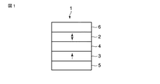
図1は、本発明の第1実施形態に係るMR素子の主要部を示している。図1は、いわゆるシングルピン構造のMR素子を示している。図1において、矢印は磁化方向を示している。本明細書および特許請求の範囲でいうMR素子とは、金属スペーサ層を用いたGMR(巨大磁気抵抗効果)素子と、半導体あるいは絶縁体をスペーサ層に用いるTMR(トンネル磁気抵抗効果)素子とを総称している。以下の図では、MR素子の主要部を示しているが、図示の構成を含んでいれば、さらなる層を含んでいても構わない。
(1) Structure of MR Element FIG. 1 shows a main part of the MR element according to the first embodiment of the present invention. FIG. 1 shows an MR element having a so-called single pin structure. In FIG. 1, the arrow indicates the magnetization direction. The MR element referred to in this specification and claims includes a GMR (giant magnetoresistive effect) element using a metal spacer layer and a TMR (tunnel magnetoresistive effect) element using a semiconductor or an insulator for the spacer layer. Collectively. In the following drawings, the main part of the MR element is shown. However, as long as the configuration shown in the figure is included, a further layer may be included.
MR素子1は、各層が相互に面する面(膜面)を貫いて流れる電流の方向に応じて、2つの定常状態の一方を取るように構成された素子である。各定常状態を、“0”データ、“1”データに対応させることによって、MR素子1は2値のデータを記憶できる。そして、MR素子1は、スピン注入書き込み(スピン注入磁化反転)方式によって、磁化の状態が変化し、この状態に応じた情報を記憶する。
The
図1に示すように、MR素子1は、少なくとも、2つの磁性層2、3と、磁性層2、3の間に設けられたスペーサ層(中間層)4を有する。磁性層2は、膜面を貫く方向、典型例として膜面に垂直な方向を向いて磁化容易軸を有し、膜面と交わる面に沿って回転する。以下、磁性層2をフリー層(自由層、磁化自由層、磁化可変層、記録層)と称する。フリー層2のより詳細な性質については後述する。以下、膜面を貫く方向の磁化を垂直磁化と称する。
As shown in FIG. 1, the
磁性層3は、その磁化を膜面と交わる方向、典型例として膜面に垂直な方向に固定されている。または、フリー層2の保持力よりも大きい保持力を有する構成とされていてもよい。以下、磁性層3を、ピン層(固定層、磁化固定層、参照層、磁化参照層、基準層、磁化基準層)と称する。典型例として、フリー層2の磁化容易軸の方向は、ピン層3の磁化の方向に沿っている。ピン層3のより詳細な性質については後述する。なお、ピン層3の磁化方向は、図では、上を向いているが、下を向いていても構わない。
The
スペーサ層(中間層)4は、非磁性金属、非磁性半導体、絶縁膜等から構成される。スペーサ層4のより詳細な性質については、後述する。
The spacer layer (intermediate layer) 4 is made of a nonmagnetic metal, a nonmagnetic semiconductor, an insulating film, or the like. More detailed properties of the
MR素子1は、いわゆる、スピン注入書込み方式に用いるMR素子である。すなわち、書き込みの際は、ピン層3からフリー層2へ、またはフリー層2からピン層3へ、膜面を貫く(典型的には膜面に垂直な)方向に電流を流すことによって、スピン情報を蓄積された電子がピン層3からフリー層2へ注入される。この注入された電子のスピン角運動量が、スピン角運動量の保存則に従ってフリー層2の電子に移動されることによって、フリー層2の磁化が反転する。
The
また、図1は、スペーサ層4の上にフリー層2が形成され、スペーサ層4の下にピン層3が形成される、いわゆるボトムピン構造を例示している。しかしながら、スペーサ層4の下にフリー層2が形成され、スペーサ層4の上にピン層3が形成される、いわゆるトップピン構造であっても構わない。
FIG. 1 illustrates a so-called bottom pin structure in which the
ピン層3の下には下地層5がさらに形成されてもよい。下地層5は、ピン層3より上の層の結晶の配向性および結晶粒径などの結晶性を制御するために用いられる。
An
フリー層2上にはキャップ層6がさらに形成されていてもよい。キャップ層6は、保護層として機能し、ボトムピン層構造のフリー層2、あるいは、トップピン層構造のピン層3を酸化から保護する。同時に、キャップ層6はポストアニールにおいて原子(分子)が拡散することを抑制する機能も有する。また、キャップ層6はフリー層2あるいはピン層4が相変化を伴う場合、格子のミスフィットなどを考慮するとエネルギー的に相変化をアシストする効果を有する場合もある。
A
図1では、後述する界面層が挿入されていない。図1の構成は、フリー層2およびピン層4が、十分なTMRを発現させたり、スピン注入効率をもたらしたりするに足るスピン分極率を有する場合に用いることができる。
In FIG. 1, the interface layer described later is not inserted. The configuration of FIG. 1 can be used when the
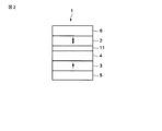
図2に示すように、フリー層2とスペーサ層4との間に界面層11が挿入されていても良い。界面層11、および後述の界面層12、13は、強磁性体からなる。界面層11乃至13のより詳細な性質については後に詳述する。界面層11は、スペーサ層4とフリー層2との界面での結晶格子ミスフィットを低減する効果も有する。すなわち、スペーサ層4上のフリー層2あるいはピン層3のバッファ層としての機能を有する。
As shown in FIG. 2, an
また、図3に示すように、ピン層3とスペーサ層4との間に界面層12が挿入されていても良い。界面層12は、MR素子1のTMR比を向上させ、スピン供給側の分極率を向上させ、スピン注入効率を向上させることを目的として挿入される。界面層12はスペーサ層4とピン層3との界面での結晶格子のミスフィットを低減する効果も有する。すなわち、ボトムピン構造またはトップピン構造に応じてピン層3上あるいはフリー層2上のスペーサ層4のバッファ層としての機能を有する。特に結晶質なスペーサ層4を用いる場合に重要となる。
As shown in FIG. 3, an
また、図4に示すように、フリー層2とスペーサ層4との間、ピン層3とスペーサ層4との間に、界面層11、12がそれぞれ挿入されていても良い。この構成により、図2、図3の説明において記載した効果の両方を得られる。
As shown in FIG. 4, interface layers 11 and 12 may be inserted between the
MR素子1は、いわゆるデュアルピン構造を有していても良い。図5は、本発明の実施形態に係るMR素子の主要部を示しており、いわゆるデュアルピン構造のMR素子を示している。
The
図5に示すように、フリー層2の、スペーサ層4と反対の面上に、さらなるスペーサ層21、さらなるピン層22が設けられている。キャップ層6は、ピン層22上に位置する。ピン層22は、ピン層3と同じく垂直磁化を有する。スペーサ層21の材料はスペーサ層4に用いられるのと同じ材料から選択することができ、ピン層22の材料はピン層3に用いられるのと同じ材料から選択することができる。ピン層3の磁化とピン層22の磁化とは反平行となっている。
As shown in FIG. 5, a
スピン注入磁化反転においては、デュアルピン構造にすることにより、電子の注入源が2箇所となる。この結果、電子の注入効率が上昇して、反転電流を下げる効果を得られる。 In the spin transfer magnetization reversal, the dual pin structure is used to provide two electron injection sources. As a result, the electron injection efficiency is increased, and the effect of reducing the reversal current can be obtained.
デュアルピン構造の場合、TMRを発現させるために、スペーサ層4、21の一方が、トンネルバリアとしての機能を有していれば良い。すなわち、スペーサ層4、21の一方が、絶縁体または半導体から形成される。また、スペーサ層4、21の一方が、Cu、Ag、Au、Pt、Pd、Al、Mgなどの金属でも構わない。スペーサ層4および21が共にトンネルバリア層である場合、スペーサ層4および21に抵抗差をつければよく、その時の面抵抗(R・A(Rは抵抗値、Aは面積を表す))の差が2倍から5倍であることが好ましい。そうすることで、スピン蓄積の効果を最大限に利用することができる。 In the case of a dual pin structure, one of the spacer layers 4 and 21 may have a function as a tunnel barrier in order to develop TMR. That is, one of the spacer layers 4 and 21 is formed from an insulator or a semiconductor. One of the spacer layers 4 and 21 may be a metal such as Cu, Ag, Au, Pt, Pd, Al, or Mg. When both the spacer layers 4 and 21 are tunnel barrier layers, a difference in resistance may be given to the spacer layers 4 and 21, and a difference in sheet resistance (R · A (R is a resistance value, A is an area)) at that time Is preferably 2 to 5 times. By doing so, the effect of spin accumulation can be maximized.
また、図6に示すように、図2と同様に、フリー層2とスペーサ層4との間に界面層11が挿入されていても良い。また、図7に示すように、フリー層2とスペーサ層21との間に界面層13が挿入されていても良い。また、図8に示すように、フリー層2とスペーサ層4との間、フリー層2とスペーサ層21との間に、界面層11、13がそれぞれ挿入されていても良い。さらに、図3と同様に、デュアルピン構造において、ピン層3とスペーサ層4との間、ピン層22とスペーサ層21との間の、一方または両方に界面層12が挿入されても良い。デュアルピン構造において、フリー層2とスペーサ層4との間、フリー層2とスペーサ層21との間に、ピン層3とスペーサ層4との間、ピン層22とスペーサ層21との間に界面層11、12、13が挿入されても良い。
Further, as shown in FIG. 6, the
なお、本明細書では垂直磁化を有する磁性層を用いたMR素子を主に扱っている。しかしながら、本発明を、面内磁化(膜面に沿った方向の磁化)を有する磁性層を用いたMR素子に適用することも可能である。 In this specification, an MR element using a magnetic layer having perpendicular magnetization is mainly handled. However, the present invention can also be applied to an MR element using a magnetic layer having in-plane magnetization (magnetization in the direction along the film surface).
(2)フリー層
フリー層2が垂直磁化を有するため、以下の利点を得られる。すなわち、垂直磁化膜は情報の保持に必要な磁気異方性エネルギーを結晶磁気異方性エネルギーで賄う。このため、垂直磁化膜を用いたMR素子に対しては、面内磁化膜を用いたMR素子と異なり、形状の制約がなくなる。このため、MR素子のアスペクト比を1まで小さくすることが可能となる。具体的には、磁気記憶装置の製造工程における最小寸法をFとすると、MR素子を、4F2で形成することが可能となる。MRAMの1つのメモリセルは、1つのMR素子と1つの選択トランジスタから構成されるので、セルサイズは、選択トランジスタの形状によって規定される。このため、サイズが4F2のMR素子が形成されたとしても、選択トランジスタが6F2のサイズを有するため、サイズが6F2のセルを有するMRAMが形成される。
(2) Free layer Since the
(2−1)フリー層に求められる性質
ある層が垂直磁化を有するためには、結晶磁気異方性エネルギーKuが高くなければならず、実効的な(有効)異方性エネルギーKeが、
Ke=Ku−2πMs2>0 ・・・(式1)
ただし、
Ms:飽和磁化
でなければ垂直磁化状態が安定ではない。したがって、安定な垂直磁化膜を形成するには、適度な実効的異方性エネルギーKeを確保することが重要である。このためには、結晶磁気異方性エネルギーKuを大きくするか、飽和磁化Msを低減することが考えられる。結晶磁気異方性エネルギーKuは、材料の性質に大きく依存するため、結晶磁気異方性エネルギーKuを大きくすることには限界がある。
(2-1) Properties Required for Free Layer In order for a layer to have perpendicular magnetization, the magnetocrystalline anisotropy energy Ku must be high, and the effective (effective) anisotropy energy Ke is
Ke = Ku−2πMs 2 > 0 (Expression 1)
However,
Ms: If the magnetization is not saturated, the perpendicular magnetization state is not stable. Therefore, in order to form a stable perpendicular magnetization film, it is important to secure an appropriate effective anisotropic energy Ke. For this purpose, it is conceivable to increase the magnetocrystalline anisotropy energy Ku or reduce the saturation magnetization Ms. Since the magnetocrystalline anisotropy energy Ku largely depends on the properties of the material, there is a limit to increasing the magnetocrystalline anisotropy energy Ku.
また、フリー層2が情報を保持するために必要な活性化エネルギーEaは、
Ea=Ke・VM
ただし、
Ke:実効磁気異方性エネルギー
VM:有効磁化体積
で表される。
The activation energy Ea necessary for the
Ea = Ke · V M
However,
Ke: Effective magnetic anisotropy energy V M : Expressed by effective magnetization volume.
ここで垂直磁化膜の実効磁気異方性エネルギーKeは、
Ke=Ku−2πMs2
で表される。Msは、飽和磁化を表す。
Here, the effective magnetic anisotropy energy Ke of the perpendicular magnetization film is
Ke = Ku-2πMs 2
It is represented by Ms represents saturation magnetization.
このように活性化エネルギーEaは、実効的異方性エネルギーKeに、ひいては、結晶磁気異方性エネルギーKuに依存する。このため、安定な垂直磁化膜を形成するために結晶磁気異方性エネルギーKuを大きくし過ぎると、情報の保持に必要な活性化エネルギーEaが大きくなり過ぎてしまうことが懸念される。 As described above, the activation energy Ea depends on the effective anisotropy energy Ke, and thus on the magnetocrystalline anisotropy energy Ku. For this reason, there is a concern that if the magnetocrystalline anisotropy energy Ku is excessively increased in order to form a stable perpendicular magnetization film, the activation energy Ea necessary for holding information is excessively increased.
以上の制約から、安定な垂直磁化膜を形成する、すなわち、十分な熱耐性を有する垂直磁化膜を形成するためには、飽和磁化Msを低減することが重要である。 In view of the above restrictions, in order to form a stable perpendicular magnetization film, that is, to form a perpendicular magnetization film having sufficient heat resistance, it is important to reduce the saturation magnetization Ms.
また、一般的に、ある層におけるスピン注入磁化反転に必要な臨界電流(磁化反転電流)Icは、
Ic∝α・η・Ms・Δ ・・・(式2)
ただし、
α:ダンピング定数
η:スピン注入効率係数
Δ:熱安定指標
である。ここで、熱安定性指標Δは、
Δ=Ke・VM/(kb・T)である。
In general, the critical current (magnetization reversal current) Ic necessary for spin injection magnetization reversal in a certain layer is
Ic∝α · η · Ms · Δ (Formula 2)
However,
α: Damping constant η: Spin injection efficiency coefficient Δ: Thermal stability index. Here, the thermal stability index Δ is
Δ = Ke · V M / (k b · T).
ただし、
VM:有効磁化体積
kb:ボルツマン定数
T:絶対温度
である。熱安定指標Δは、ある層に記録された情報の保持能力の指標となる。したがって、熱安定指標Δは維持しつつ飽和磁化Msを低減することが、磁化反転電流を下げ且つ情報の保持能力を上げることにつながる。
However,
V M : Effective magnetization volume k b : Boltzmann constant T: Absolute temperature. The thermal stability index Δ is an index of the ability to retain information recorded in a certain layer. Therefore, reducing the saturation magnetization Ms while maintaining the thermal stability index Δ leads to a decrease in magnetization reversal current and an increase in information retention capability.
以上の事項を考慮して、フリー層2として、垂直磁化および高い熱安定指標を保てるように正の範囲で高い値の実効的磁気異方性エネルギーを維持しながら、小さな結晶磁気異方性エネルギーKuおよび飽和磁化Msを有する材料が好ましい。
In consideration of the above matters, the
(2−2)フリー層の具体例
(2−2−1)性質
上記のように、ある層が、垂直磁化を有し、少ない電流で磁化が反転し、高い情報保持能力を有するには、正の範囲で高い値の実効的磁気異方性エネルギーKeを保ちつつ、活性化エネルギーEaを抑制できる程度に小さい結晶磁気異方性エネルギーKuと小さい飽和磁化Msとを有する材料が好ましい。このような要請を満たす材料として、以下の材料が考えられる。
(2-2) Specific Example of Free Layer (2-2-1) Properties As described above, a certain layer has perpendicular magnetization, magnetization is reversed with a small current, and high information retention capability. A material having a magnetocrystalline anisotropy energy Ku and a small saturation magnetization Ms that are small enough to suppress the activation energy Ea while maintaining a high effective magnetic anisotropy energy Ke in a positive range is preferable. The following materials can be considered as materials satisfying such requirements.
第1実施形態に係るMR素子1のフリー層2は、Fe、Co、Niから選ばれる少なくとも1つ以上の元素Aと、Ru、Rh、Pd、Ag、Re、Os、Ir、Pt、Auから選ばれる少なくとも1つ以上の元素Bと、V、Cr、Mnから選ばれる少なくとも1つ以上の元素Cとを含有する磁性体合金から構成される。
The
元素B(Ru、Rh、Pd、Ag、Re、Os、Ir、Pt、Au)は、多くの4d電子および5d電子を有している。3d、4d、5d電子を多く有する元素は、高い結晶磁気異方性エネルギーを有する。このため、元素Aと元素Bからなる合金(AB合金と称する)は、高い結晶磁気異方性エネルギーKuを有し、正の高い値の実効的磁気異方性エネルギーKeを有する。なお、AB合金は、フェロ磁性合金である。元素Bの組成は、30at%以上70at%以下であることが好ましい。その理由は、下記で詳細を説明するが、この組成領域において、1x10⁶erg/cc以上の大きな結晶磁気異方性エネルギーKuを有するL10規則構造相を有することが可能だからである。 Element B (Ru, Rh, Pd, Ag, Re, Os, Ir, Pt, Au) has many 4d electrons and 5d electrons. Elements having many 3d, 4d, and 5d electrons have high magnetocrystalline anisotropy energy. For this reason, an alloy composed of the elements A and B (referred to as an AB alloy) has a high magnetocrystalline anisotropy energy Ku, and has a positive positive effective magnetic anisotropy energy Ke. The AB alloy is a ferromagnetic alloy. The composition of element B is preferably 30 at% or more and 70 at% or less. The reason for this will be described in detail below, because it is possible to have an L1 0 ordered structure phase having a large magnetocrystalline anisotropy energy Ku of 1 × 10 6 erg / cc or more in this composition region.
AB合金のうちで、特に、室温において垂直磁化特性を示すものとしては、FePt合金、FePd合金、CoPt合金、CoPd合金、NiPt合金が挙げられる。ここで、垂直磁気異方性を示す条件としては、実効磁気異方性エネルギーKe>0であることである。これらの合金は、元素Aの組成比が40乃至60at%の範囲内で、面心正方(FCT : face-centered tetragonal)構造を基本格子として有するL10型(CuAu型)規則構造相を安定相として有している。L10規則構造相は、基本的にFCT構造を基本格子としており、単位胞の格子定数(a,b,c)の関係は、a=b、a≠c、a>cである。また、元素Aの組成比が30乃至70at%の範囲においても、L10規則構造相が形成される。ここで、L10構造層は、体積比で50%以上である。L10規則構造層では元素Aで形成される(001)面であるA面、および、元素Bで形成される(001)面であるB面が、[001]方向に、A面、B面、A面、B面、A面・・・・のように交互に積層される。L10規則相においては、X線回折あるいは電子ビーム回折において、規則化に伴う禁制反射が観測される。すなわち、FCT構造で見られる(002)面に起因する回折像と同時に、(001)面に起因する回折像も得られることになる。 Among the AB alloys, those that exhibit the perpendicular magnetization characteristics particularly at room temperature include FePt alloys, FePd alloys, CoPt alloys, CoPd alloys, and NiPt alloys. Here, the condition indicating the perpendicular magnetic anisotropy is that the effective magnetic anisotropy energy Ke> 0. These alloys within the composition ratio of the element A is 40 to 60at%, a face-centered tetragonal (FCT: face-centered tetragonal) structure L1 0 type having as a basic grid (CuAu type) ordered structure phase stable phase Have as. The L1 0 ordered structure phase basically has an FCT structure as the basic lattice, and the relation of the lattice constants (a, b, c) of the unit cell is a = b, a ≠ c, a> c. The composition ratio of the element A is also in the range of 30 to 70 at%, L1 0 ordered structure phase is formed. Here, the L1 0 structure layer is 50% or more by volume ratio. In the L1 0 ordered structure layer, the A plane that is the (001) plane formed by the element A and the B plane that is the (001) plane formed by the element B are in the [001] direction in the A plane and the B plane. , A surface, B surface, A surface,... In the L1 0 ordered phase, forbidden reflection accompanying ordering is observed in X-ray diffraction or electron beam diffraction. That is, a diffraction image attributed to the (001) plane can be obtained simultaneously with a diffraction image attributed to the (002) plane seen in the FCT structure.
また、上述したABABABという積層構造を有するL10構造は、スパッタリング法あるいはMBE法(モレキュラー・ビーム・エピタキシー法)によって、多数の周期を有する人工格子によっても人工的に形成が可能である。従って、必ずしも、2元系あるいは3元系相状態図に安定相として存在する必要性はない。 Also, L1 0 structure having a laminated structure of ABABAB described above, the sputtering method or MBE method by (molecular beam epitaxy), it is possible to artificially formed by an artificial lattice having a large number of cycles. Therefore, it is not always necessary to exist as a stable phase in the binary or ternary phase diagram.
また、元素Aの組成比が30乃至50at%の範囲では、AB3で表されるL12規則構造相が局所的に形成されることがある。また、元素Aの組成比が50乃至70at%の範囲では、A3Bで表されるL12規則構造相が局所的に形成されることがある。 In addition, when the composition ratio of the element A is in the range of 30 to 50 at%, the L1 2 ordered structure phase represented by AB 3 may be locally formed. In addition, when the composition ratio of the element A is in the range of 50 to 70 at%, an L1 2 ordered structure phase represented by A 3 B may be locally formed.
L10構造のAB合金は、高い一軸結晶磁気異方性エネルギーKuを[001]方向に有しており、(001)面が膜面に対して平行に優先配向すると垂直磁化が安定となる。しかしながら、L10規則構造相を有する2元系のAB合金では、飽和磁化Msが1000emu/cc程度と大きい。このため、磁化反転電流Icを下げるためには、飽和磁化Msを小さくする必要がある。飽和磁化Msを小さくする際に、同時に、正の高い値の実効的磁気異方性エネルギー(Ke>0)を維持できる程度に高く且つ活性エネルギーEaを小さく抑える程度に小さな結晶磁気異方性エネルギーKuを維持しなければならない。 The AB alloy having an L1 0 structure has a high uniaxial crystal magnetic anisotropy energy Ku in the [001] direction, and when the (001) plane is preferentially oriented parallel to the film surface, the perpendicular magnetization becomes stable. However, the binary AB alloy having the L1 0 ordered structure phase has a saturation magnetization Ms as large as about 1000 emu / cc. For this reason, in order to lower the magnetization reversal current Ic, it is necessary to reduce the saturation magnetization Ms. When the saturation magnetization Ms is reduced, at the same time, the magnetocrystalline anisotropy energy is high enough to maintain a positive positive effective magnetic anisotropy energy (Ke> 0) and small enough to keep the active energy Ea small. Ku must be maintained.
一般的に、フェロ磁性体に非磁性元素を添加していくと、添加量にほぼ比例する形で飽和磁化Msおよび結晶磁気異方性エネルギーKuが低下する。しかしながら、結晶磁気異方性エネルギーKuの低下率のほうが、飽和磁化Msの低下率より大きい。このため、非磁性元素の添加量の増加に伴い、式1から分かるように、実効的磁気異方性エネルギーKe>0を維持できず、垂直磁化を維持するのが非常に困難となる。
In general, when a nonmagnetic element is added to a ferromagnetic material, the saturation magnetization Ms and the magnetocrystalline anisotropy energy Ku decrease in a manner that is approximately proportional to the amount added. However, the rate of decrease in magnetocrystalline anisotropy energy Ku is greater than the rate of decrease in saturation magnetization Ms. For this reason, as the amount of nonmagnetic element added increases, as can be seen from
そこで、フェロ磁性体であるL10構造のAB合金をフェリ磁性体化すればよい。フェリ磁性体を作成する方法としては、フェロ磁性体に、反強磁性的振る舞いをする元素を添加することが挙げられる。このために、AB合金に元素Cが添加される。元素Cは、元素Aに対して置換型で固溶することが好ましい。ここで、反強磁性的な振る舞いをする元素Cとして、上記のように、V、Cr、Mnがある。AB合金をフェリ磁性体化することによって、正の高い値の実効異方性エネルギーKeを維持しつつ、結晶磁気異方性エネルギーKuと実効的な飽和磁化Ms(ネットMs)とを小さく抑制することができる。元素Cを元素Aと置換する場合、ネットの飽和磁化Msが0以上となるように添加しなくてはならない。ネットの飽和磁化Msがゼロになる組成は、補償点組成と呼ばれ、本発明のL10構造のAB合金の場合、元素Cの置換量が全体に対して25%未満となることが好ましい。すなわち、元素Aと元素Cの原子組成比はA:C=50:50(at%)、換言すれば元素Aに対する元素Cの組成比が1以下(0を除く)が最大の置換量となる。これを超えるとABC合金は反強磁性合金となり、TMR比が激減する。 Therefore, the AB alloy of L1 0 structure is ferro-magnetic material may be ferrimagnetic body of. As a method for producing a ferrimagnetic material, an element having antiferromagnetic behavior is added to the ferromagnetic material. For this purpose, the element C is added to the AB alloy. The element C is preferably dissolved in substitutional form with respect to the element A. Here, as described above, there are V, Cr, and Mn as the element C that behaves antiferromagnetically. By making the AB alloy a ferrimagnetic material, the magnetocrystalline anisotropy energy Ku and the effective saturation magnetization Ms (net Ms) are suppressed to a small value while maintaining a positive positive effective anisotropy energy Ke. be able to. When the element C is replaced with the element A, it must be added so that the saturation magnetization Ms of the net becomes 0 or more. Composition saturation magnetization Ms of the net is zero is called the compensation point composition, when the L1 0 structure AB alloy of the present invention, it is preferred that less than 25% relative to the total replacement of the element C. That is, the atomic composition ratio of element A and element C is A: C = 50: 50 (at%). In other words, the maximum substitution amount is when the composition ratio of element C to element A is 1 or less (except 0). . Above this, the ABC alloy becomes an antiferromagnetic alloy, and the TMR ratio is drastically reduced.
元素Bとして、元素Aと元素Cとからなる材料が、フェリ的な磁化配列を維持しながら、高い結晶磁気異方性エネルギーKuを有し、ひいては正の高い値の実効的磁気異方性エネルギーKeを維持できるものが選択されている。元素Bは、4d電子、5d電子を多く有する元素である。このような元素として、他にも該当するものがあるが、これらは空き準位を有していないか非常に少ないため、元素A、Cからなる材料の結晶磁気異方性エネルギーKuの増加に寄与しない。そこで、本実施形態では、上に列挙した元素Bが用いられている。ただし、電子数的にいうと5d、4f元素を含まないB元素がダンピング定数低減、すなわち、スピン注入磁化反転電流の低減には好ましく、この観点からいうと、元素Bとしては、Ru、Rh、Pd、Agが好ましい。 A material composed of the elements A and C as the element B has a high magnetocrystalline anisotropy energy Ku while maintaining a ferrimagnetic magnetization arrangement, and thus a high positive effective magnetic anisotropy energy. Those capable of maintaining Ke are selected. Element B is an element having many 4d electrons and 5d electrons. There are other such elements, but these elements have no vacancies or are very small, and therefore increase the magnetocrystalline anisotropy energy Ku of the material composed of the elements A and C. Does not contribute. Therefore, in the present embodiment, the element B listed above is used. However, in terms of the number of electrons, the B element not including the 5d and 4f elements is preferable for reducing the damping constant, that is, reducing the spin-injection magnetization reversal current. From this viewpoint, as the element B, Ru, Rh, Pd and Ag are preferred.
このように、フリー層2が、元素A、B、Cを含んだ材料から構成される。フリー層2が元素A、Bの合金から構成されることによって、フリー層2の実効的磁気異方性エネルギーKeを正の範囲で高く維持することができる。同時に、元素A、Cによってフェリ磁性体を構成することによって、実効的磁気異方性エネルギーKeを正の範囲で高く維持しつつ結晶磁気異方性エネルギーKuおよび飽和磁化Msの小さなフリー層2を実現できる。この結果、フリー層2の垂直磁化を維持しやすい状態を保ちながら、磁化反転電流Icおよび活性化エネルギーEaを小さくすることができる。
Thus, the
本実施形態では、3d遷移元素をフェリ磁性体化して、フリー層2に用いている。これに対して、希土類元素を用いてフェリ磁性体を実現することも考えられる。希土類元素を用いると、フェリ磁性体の飽和磁化Msを正負両方の範囲で制御することができるので、飽和磁化Msの制御の観点からは望ましい。しかしながら、希土類元素を用いたフェリ磁性体、例えばFeCo−RE材料(REは希土類元素)は、アモルファス構造を有し、アモルファス構造が崩れるとフェロ磁性体となってしまう。また、希土類元素は耐食性が非常に低い。このように、希土類元素は、フリー層2に用いるには、扱いが難しい。また、スピン注入書き込み用のMR素子では、飽和磁化Msを最低で0まで低下できれば十分であり、飽和磁化に負の値を持たせることは求められない。以上の要素を考慮して、本実施形態では、元素Aと元素Cを用いてフェリ磁性金属を実現している。
In the present embodiment, the 3d transition element is converted into a ferrimagnetic material and used for the
また、フリー層2の材料として、MnAl合金を用いることができる。MnAl合金によっても、実効的磁気異方性エネルギーKeを正の範囲で高く維持しつつ結晶磁気異方性エネルギーKuおよび飽和磁化Msの小さなフリー層2を実現できる。
Further, a MnAl alloy can be used as the material of the
また、垂直磁化を有するフェリ磁性金属を得る方法として、貴金属元素と3d遷移金属元素による反強磁性合金に強磁性元素Fe、Co、Niを添加することも可能である。貴金属元素と3d遷移金属元素による反強磁性合金は、RhFe合金、PdMn合金、PtMn合金、PtCr合金、RhMn合金、AuMn合金、AuCr合金、CrMn合金、PdCr合金、RuCr合金、ReCr合金などがある。これらの反強磁性の2元系合金は、おおよそ1:1の組成比である。ただし、厳密な意味ではなく、含有可能なRh、Pt、Pd、Au、Re、Ruの原子組成は、40at%から60at%の範囲である。 Further, as a method for obtaining a ferrimagnetic metal having perpendicular magnetization, it is also possible to add ferromagnetic elements Fe, Co, and Ni to an antiferromagnetic alloy composed of a noble metal element and a 3d transition metal element. Antiferromagnetic alloys composed of noble metal elements and 3d transition metal elements include RhFe alloys, PdMn alloys, PtMn alloys, PtCr alloys, RhMn alloys, AuMn alloys, AuCr alloys, CrMn alloys, PdCr alloys, RuCr alloys, and ReCr alloys. These antiferromagnetic binary alloys have a composition ratio of approximately 1: 1. However, this is not a strict meaning, and the atomic composition of Rh, Pt, Pd, Au, Re, and Ru that can be contained is in the range of 40 at% to 60 at%.
これら合金の中では、RhMn合金、AuMn合金、AuCr合金、CrMn合金、PdCr合金、RuCr合金、ReCr合金などは結晶磁気異方性エネルギーKuが小さいために垂直磁気異方性を示さない可能性が高い。これらに対しては、Ptを添加することで、結晶磁気異方性エネルギーKuを上げることが可能である。 Among these alloys, RhMn alloy, AuMn alloy, AuCr alloy, CrMn alloy, PdCr alloy, RuCr alloy, ReCr alloy, etc. may not show perpendicular magnetic anisotropy because of low magnetocrystalline anisotropy energy Ku. high. For these, the magnetocrystalline anisotropy energy Ku can be increased by adding Pt.
フェリ磁性体であることを調べるには、XMCD法を用いるとよい。XMCDとは、X-ray Magnetic circular dichroismの略であり、X線磁気円二色性測定法という。XMCD法により、A元素およびB元素、さらには、C元素が磁性を有する場合において、各元素についての磁化応答曲線を取得することが可能である。これにより、含有元素の磁気特性を分解できるため、磁場の応答性が元素ごとで異なれば、フェリ磁性体であることが判別できる。 The XMCD method may be used to examine the ferrimagnetic material. XMCD is an abbreviation for X-ray Magnetic circular dichroism and is called an X-ray magnetic circular dichroism measurement method. By the XMCD method, when the A element, the B element, and further the C element have magnetism, it is possible to obtain a magnetization response curve for each element. Thereby, since the magnetic characteristics of the contained element can be decomposed, if the responsiveness of the magnetic field differs for each element, it can be determined that the element is a ferrimagnetic material.
また、フリー層2は、以下の面関係および方位関係を有することができる。すなわち、NaCl構造を有する酸化物層上に、
面関係:NaCl構造酸化物(100)//L10構造合金(001)
方位関係:NaCl構造酸化物[100]//L10構造合金[100]
で結晶成長させることによって、L10規則構造のc軸が膜面に対して垂直な層を形成することが可能となる。ここで、//は、平行であることを意味している。そこで、後述のように、スペーサ層4として用いることができるNaCl構造を有する酸化物層上に、上記の面関係および方位関係を持って結晶成長させることができる。これにより、より安定な垂直磁化を実現できる。
Moreover, the
Surface relationship: NaCl structure oxide (100) // L1 0 structure alloy (001)
Orientation relationship: NaCl structure oxide [100] // L1 0 structure alloy [100]
It is possible to form a layer in which the c-axis of the L1 0 ordered structure is perpendicular to the film surface. Here, // means parallel. Therefore, as will be described later, a crystal can be grown on the oxide layer having the NaCl structure that can be used as the
(2−2−2)実施例(FePt合金)
具体的な実施例として、FePt合金膜へのMnの添加について説明する。
(2-2-2) Example (FePt alloy)
As a specific example, the addition of Mn to the FePt alloy film will be described.
FePt合金は、Feの組成比がおおよそ50at%(30at%から70at%の範囲)でL10構造を主構造とする。Feの組成比がPtの組成比より大きくなるとFe3Pt組成のL12構造合金が部分的に形成されやすく、Ptの組成比がFeの組成比より大きくなるとFePt3組成のL12構造合金が部分的に形成されやすくなる。 FePt alloys, the L1 0 structure and the main structure at the composition ratio of Fe is approximately 50at% (ranging from 30 at% of 70 at%). When the Fe composition ratio is larger than the Pt composition ratio, an L1 2 structural alloy having an Fe 3 Pt composition is likely to be partially formed, and when the Pt composition ratio is larger than the Fe composition ratio, an L1 2 structural alloy having an FePt 3 composition is formed. It becomes easy to form partially.
L10構造のFePt合金は、a=0.385nm±0.005nm、c=0.371nm±0.005nm、c/a≒0.96を有するFCT格子を有する規則相合金である。L10構造のFePt合金は、飽和磁化Msが800emu/cc、結晶磁気異方性エネルギーKu>1×107erg/ccを有し、理想的な高Ku膜である。 The FePt alloy having the L1 0 structure is an ordered phase alloy having an FCT lattice having a = 0.385 nm ± 0.005 nm, c = 0.371 nm ± 0.005 nm, and c / a≈0.96. The FePt alloy having the L1 0 structure is an ideal high Ku film having a saturation magnetization Ms of 800 emu / cc and a magnetocrystalline anisotropy energy Ku> 1 × 10 7 erg / cc.
FePt合金にV、Cr、Mnを添加することにより、結晶磁気異方性エネルギーKuおよび飽和磁化Msを小さくすることが可能である。V、Cr、MnはFeサイトへ置換型で添加される。置換されたV、Cr、Mnは、磁気モーメントを持つが、Feとは反平行の磁化方向を有する。この結果、V、Cr、Mnを添加されたFePt膜全体としてはフェリ磁性体となる。このことは、Ptを部分的あるいは全体をPdで置換した場合にも同様である。 By adding V, Cr, or Mn to the FePt alloy, it is possible to reduce the magnetocrystalline anisotropy energy Ku and the saturation magnetization Ms. V, Cr, and Mn are added to the Fe site in a substitutional form. The substituted V, Cr, and Mn have a magnetic moment but have a magnetization direction antiparallel to Fe. As a result, the entire FePt film to which V, Cr, and Mn are added becomes a ferrimagnetic material. The same applies to the case where Pt is partially or entirely replaced with Pd.
図9には、5nmの厚さを有する、L10構造のFePt膜へのMnの添加量と、飽和磁化Msおよび垂直磁化保磁力Hc⊥と、の関係を示した。FeMnPt膜のMn原子の組成比で25at%まで、すなわちFeとの置換率で50%程度までは、垂直磁化特性を維持しながら、結晶磁気異方性エネルギーKuおよび飽和磁化Msを低減できることが分かった。 FIG 9 has a thickness of 5 nm, it showed the addition amount of Mn in the FePt film of L1 0 structure, and the saturation magnetization Ms and the perpendicular magnetic coercive force Hc⊥, the relationship. It can be seen that the magnetocrystalline anisotropy energy Ku and the saturation magnetization Ms can be reduced while maintaining the perpendicular magnetization characteristics up to 25 at% in the composition ratio of Mn atoms in the FeMnPt film, that is, up to about 50% in substitution rate with Fe. It was.
飽和磁化MsはMnの添加量に応じて減少し、Mnの添加量が25at%付近で400emu/cc程度の垂直保持力が得られた。また、MgOからなるスペーサ層4上に、厚さ1nmのFeからなる界面層11、FeMnPt合金膜からなるフリー層2を形成し、フリー層2が垂直磁化を有することを確認した。
The saturation magnetization Ms decreased according to the added amount of Mn, and a perpendicular coercive force of about 400 emu / cc was obtained when the added amount of Mn was around 25 at%. Further, an
(2−2−3)実施例(MnAl合金)
別の具体的な実施例として、MnAl合金について説明する。
(2-2-3) Example (MnAl alloy)
As another specific example, a MnAl alloy will be described.
MnAl合金は、Mnの組成比が30乃至70at%の付近で、L10構造規則相を有する。より安定にL10構造規則相を形成するためには、Mnの組成比が40乃至60at%であることが好ましい。MnAl合金は、100emu/cc以下の飽和磁化Msで、かつ5×105erg/cc以上の高い結晶磁気異方性エネルギーKuを有する。バルク的なキュリー点は、およそ645Kである。相図上、τ相あるいはε’相と呼ばれる。単位胞をFCT構造とすると、a=0.394nm、c=0.358nm、c/a=0.908である。 MnAl alloy, the composition ratio of Mn is in the vicinity of 30 to 70 at%, having an L1 0 structure ordered phase. In order to form a more stable L1 0 structure ordered phase is preferably the composition ratio of Mn is 40 to 60at%. The MnAl alloy has a saturation magnetization Ms of 100 emu / cc or less and a high magnetocrystalline anisotropy energy Ku of 5 × 10 5 erg / cc or more. The bulk Curie point is approximately 645K. On the phase diagram, it is called τ phase or ε 'phase. When the unit cell has an FCT structure, a = 0.394 nm, c = 0.358 nm, and c / a = 0.908.
L10構造のMnAl合金は、Mnの組成比が50at%で強磁性体である。Mnの組成比がこれよりも多くなると、MnのAlサイトへの置換が起こり、AlサイトのMnは、MnサイトのMnと反平行なスピン配列をとる。この結果、このようなMnAl合金は、フェリ磁性体となる。 MnAl alloy of L1 0 structure, the composition ratio of Mn is ferromagnetic at 50at%. When the composition ratio of Mn is larger than this, substitution of Mn to Al sites occurs, and Mn at the Al site takes a spin arrangement antiparallel to Mn at the Mn site. As a result, such a MnAl alloy becomes a ferrimagnetic material.
Alの原子組成が50at%以上の場合においても、Mn50Al50(at%)をAlで希釈する効果となる。したがって、結晶磁気異方性エネルギーKuも単純に減少し、同時に、飽和磁化Msも低下する。従って、L10構造のMnAl規則相を析出させることが、高い結晶磁気異方性エネルギーKuの維持のためには必要である。その観点から、L10構造のMnAl規則相を析出させるためには、Alの原子組成は70at%以下であることが好ましいといえる。 Even when the atomic composition of Al is 50 at% or more, Mn 50 Al 50 (at%) is diluted with Al. Accordingly, the magnetocrystalline anisotropy energy Ku is simply reduced, and at the same time, the saturation magnetization Ms is also lowered. Therefore, it is necessary to precipitate the MnAl ordered phase having the L1 0 structure in order to maintain a high magnetocrystalline anisotropy energy Ku. From this point of view, in order to precipitate the L1 0 structure MnAl ordered phase of the atomic composition of Al can be said that it is preferably not more than 70 at%.
L10構造のMnAl合金は、低い飽和磁化Msで高い結晶磁気異方性エネルギーKuを有するがために、高い活性化エネルギーEaを有する。そこで、活性化エネルギーEaを適切な値へと調整するために、第3の元素Xおよび第4の元素Yが添加される。また、第3の元素Xは、MnAl合金の分極率を向上させ、TMR比を向上させる効果も有する。同時に、第3の元素Xは、飽和磁化Msを上げて、活性化エネルギーEaを下げるための添加元素である。 The MnAl alloy having the L1 0 structure has a high crystal energy anisotropy energy Ku with a low saturation magnetization Ms, and therefore has a high activation energy Ea. Therefore, in order to adjust the activation energy Ea to an appropriate value, the third element X and the fourth element Y are added. The third element X also has the effect of improving the polarizability of the MnAl alloy and improving the TMR ratio. At the same time, the third element X is an additive element for increasing the saturation magnetization Ms and decreasing the activation energy Ea.
第3の元素Xとしては、Fe、Co、Niがある。Fe、Co、Ni元素は、Mnサイトに置換型に配置される。これにより、MnXAlとなり、飽和磁化Msが増大するために、実効的な垂直磁化の結晶磁気異方性エネルギーKu−effectを下げることが可能となり、これによっても活性化エネルギーEaを下げることができる。ここで、Ku−effectは、
Ku−effect=Ku−2πMs2
で表される。第3の元素Xは、Mnサイトに置換されるが、置換する量としては、Mnと元素Xの原子組成比で、1以下(0を除く)であることが好ましい。これは、Feの原子組成比が1を超えると、急激に飽和磁化Msが増大すると考えられるからである。
The third element X includes Fe, Co, and Ni. Fe, Co, and Ni elements are arranged in substitutional form at the Mn site. Thereby, since it becomes MnXAl and the saturation magnetization Ms increases, it becomes possible to reduce the crystal magnetic anisotropy energy Ku-effect of effective perpendicular magnetization, and this can also reduce the activation energy Ea. Here, Ku-effect is
Ku-effect = Ku-2πMs 2
It is represented by The third element X is substituted at the Mn site. The substitution amount is preferably 1 or less (excluding 0) in terms of the atomic composition ratio of Mn to the element X. This is because when the atomic composition ratio of Fe exceeds 1, it is considered that the saturation magnetization Ms rapidly increases.
また、第3の元素Xの添加量は、第4の元素Yの添加量によっても、上記の範囲内で依存関係がある。飽和磁化Msを上げる際、垂直磁化特性を維持するためには、実効的磁気異方性エネルギーKe>0を確保することが求められる。第3の元素Xを添加し、高いTMRを発揮しつつ、実効的な垂直磁化の結晶磁気異方性エネルギーKu−effectを0以上に維持するためには、第3の元素Xの添加による飽和時Msの増大分の結晶磁気異方性エネルギーKuを増大させる必要が出てくる場合がある。この場合、第4の元素YであるRu、Rh、Pd、Ag、Re、Os、Ir、Pt、Auを添加する必要が出てくる。結晶磁気異方性エネルギーKuの増大の効果としては、PtとPdが好ましい添加元素と言えるので、可能な範囲で、PtあるいはPdを含めて添加するのが良い。第4の元素Yは、第3の元素XおよびMnと相互作用し、結晶磁気異方性エネルギーKuを増大させる効果がある。第4の元素Yの添加量は、第3の元素Xの添加量に依存関係があるが、MnAl合金をベースに考えると、Alに対する原子組成比で1以下であることが好ましい。 Further, the addition amount of the third element X also has a dependency within the above range depending on the addition amount of the fourth element Y. When increasing the saturation magnetization Ms, in order to maintain the perpendicular magnetization characteristics, it is required to ensure effective magnetic anisotropy energy Ke> 0. In order to maintain the effective perpendicular magnetization of magnetocrystalline anisotropy energy Ku-effect to 0 or more while adding the third element X and exhibiting high TMR, saturation due to the addition of the third element X It may be necessary to increase the magnetocrystalline anisotropy energy Ku corresponding to the increase in time Ms. In this case, it is necessary to add the fourth element Y, Ru, Rh, Pd, Ag, Re, Os, Ir, Pt, and Au. As an effect of increasing the magnetocrystalline anisotropy energy Ku, it can be said that Pt and Pd are preferable additive elements. Therefore, it is preferable to add Pt or Pd as much as possible. The fourth element Y interacts with the third element X and Mn and has an effect of increasing the magnetocrystalline anisotropy energy Ku. The amount of addition of the fourth element Y depends on the amount of addition of the third element X, but considering the MnAl alloy as a base, the atomic composition ratio with respect to Al is preferably 1 or less.
また、MnAl合金は、NaCl構造を有する酸化物層上に、下記の面関係および方位関係を持って結晶成長させることができる。 Further, the MnAl alloy can be crystal-grown on the oxide layer having the NaCl structure with the following plane relationship and orientation relationship.
面関係:NaCl構造酸化物(100)//L10構造MnAl合金(001)
方位関係:NaCl構造酸化物[100]//L10構造MnAl合金[100]
この規則に沿って形成されることにより、L10構造結晶のMnAlのc軸を膜面に対して垂直にすることが可能となり、より安定な垂直磁化を実現できる。例えば、MgOの(100)面上では、MnAl合金が(100)面の優先配向で成長すると、格子ミスフィット量は、非常に小さい。
Surface relationship: NaCl structure oxide (100) // L1 0 structure MnAl alloy (001)
Orientation relationship: NaCl structure oxide [100] // L1 0 structure MnAl alloy [100]
By being formed along this rule, it is possible to perpendicular to the film plane c-axis of MnAl of L1 0 structure crystal, it is possible to realize a more stable magnetization perpendicular. For example, on the (100) plane of MgO, when the MnAl alloy grows with the preferred orientation of the (100) plane, the amount of lattice misfit is very small.
高いTMR比を狙う場合においては、後述する界面層を挿入することが好ましい。より具体的には、例えば、MgOからなるスペーサ層4上に、厚さ2nmのFeからなる界面層11、厚さ5nmのMnAlからなるフリー層2が積層された構成が取られる。
When aiming at a high TMR ratio, it is preferable to insert an interface layer described later. More specifically, for example, a configuration is adopted in which an
(3)スペーサ層
次に、スペーサ層についてより詳しく説明する。以下の説明で、スペーサ層4と記載した場合、スペーサ層21も含むことが意図されている。
(3) Spacer layer Next, the spacer layer will be described in more detail. In the following description, when the
スペーサ層4の材料として、従来のアモルファス構造を有するAlOx酸化物よりは、NaCl構造を有する酸化物が好ましい。NaCl構造を有する酸化物としては、MgO、CaO、SrO、TiO、VO、NbOなどがある。これらの酸化物は安定相としてNaCl構造を有する。これらのNaCl構造酸化物は、Fe、Co、Niを主成分として含む、例えばアモルファスCoFeNiB合金上、あるいは体心立方(BCC : body-centered cubic)構造で(100)優先配向面を有するFeCoNi合金あるいは単元素金属上、FCT構造の層の(001)面で結晶成長させると、(100)面を優先配向面として成長しやすい。特に、B、C、Nなどを添加したCoFeアモルファス合金上では、非常に容易に(100)面を優先配向させることが可能である。
As a material for the
上記の酸化物の格子定数を示す。 The lattice constant of the above oxide is shown.
MgO:0.42112nm
CaO:0.48105nm
SrO:0.51602nm
TiO:0.41766nm
VO:0.4062nm
NbO:0.42101nm
格子の伸縮もあるので、実際のX線での格子定数測定では、上記の格子定数に±0.01nm程度の誤差を生じる。
MgO: 0.42112 nm
CaO: 0.48105 nm
SrO: 0.51602 nm
TiO: 0.41766 nm
VO: 0.4062nm
NbO: 0.42101 nm
Since there is expansion and contraction of the lattice, an error of about ± 0.01 nm occurs in the lattice constant in the actual lattice constant measurement with X-rays.
上記の(100)面に優先配向した酸化物層上では、L10構造の層は、(001)面優先配向の場合、格子の整合性が良く、ミスフィットが10%以下である。 On the oxide layer preferentially oriented in the (100) plane, the layer having the L1 0 structure has good lattice matching and a misfit of 10% or less in the case of the (001) plane preferential orientation.
フリー層2の磁化とピン層3の磁化とが反平行であると、スピン分極したΔ1バンドがトンネル伝導の担い手となるため、マジョリティースピン電子しか伝導に寄与できなくなる。この結果、MR素子1の伝導率Gが低下し、抵抗値が大きくなる。反対に、フリー層2の磁化とピン層3の磁化とが平行であると、スピン偏極していないΔ5バンドが伝導を支配するために、MR素子1の伝導率Gが上昇し、抵抗値が小さくなる。したがって、Δ1バンドの形成が高TMRを出すためのキーとなる。Δ1バンドを形成するためには、NaCl構造の酸化物からなるスペーサ層4の(100)面とフリー層2との界面が整合性よくつながらなければならない。
If the magnetization of the
NaCl構造の酸化物層のからなるスペーサ層4の(100)面での格子整合性をさらに良くするために、界面層11が挿入される。界面層11として、スペーサ層4との(100)面での格子整合が、5%以下となるような材料を選択することがΔ1バンド形成には好ましい。
In order to further improve the lattice matching on the (100) plane of the
(4)ピン層
次に、ピン層3についてより詳しく説明する。以下の説明で、スペーサ層3と記載した場合、ピン層22も含むことが意図されている。
(4) Pin Layer Next, the
垂直磁化を有するピン層3は、フリー層2より厚く、飽和磁化Msと厚さtの積あるいは結晶磁気異方性エネルギーKuがフリー層2より十分に大きいことが好ましい。これは、ピン層3内でのスピン蓄積効果、すなわち、磁化スピンから伝導電子への角運動量の移動を効率よく行うためであり、フリー層2からのスピンの注入によりピン層3の磁化が揺らぐことを最小限に抑えるためである。
The pinned
ピン層3が垂直磁化を有する場合、ピン層3からの漏洩磁場を低減することが好ましい。ピン層3の漏洩磁場は、スピン注入によってフリー層2の磁化とピン層3の磁化方向を平行から反平行にする磁化反転を阻害する。したがって、ピン層3の見かけ上の飽和磁化Ms(net−Ms)は小さい方が良い。
When the pinned
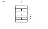
このための1つの方法として、ピン層3をシンセティックアンチフェロ(SAF)構造とすることができる。SAF構造のピン層3は、図10に示すように、強磁性層3a、中間層3b、磁性層3cの積層構造からなる。強磁性層3aと強磁性層3cは、反平行な磁化配列で安定となるように構成されている。中間層3bとしては、例えばRuやOsなどの元素が用いられる。
As one method for this purpose, the pinned
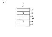
また、垂直磁化を有するピン層3の漏洩磁場を減ずるため別の方法として、ピン層3をフェリ磁性材料から構成することができる。この場合、図11に示すように、ピン層3とスペーサ層4との界面に界面ピン層23を挿入し、MR比を発現させる。フェリ磁性材料としては、FeCo−RE材料が代表的である。REとしては、Gd、Tb、Dy、Hoが垂直磁化を安定化する意味では好ましい。FeCo−RE合金はアモルファス構造である。FeCo−RE合金では、補償点付近のRE組成で、飽和磁化Msがほぼゼロになり、飽和磁化Msの担い手がFeCoからRE元素へと移り、保持力Hcが極大化する。よって、RE元素が50at%を超える組成にすることで、界面ピン層23とピン層3を合わせた見かけ上の飽和磁化net−Msをほぼゼロに設定できる。なお、これらの材料をピン層3に用いても、フリー層2について述べた問題は生じない。
As another method for reducing the leakage magnetic field of the pinned
スピン注入書き込み用の、垂直磁化を有するMR膜1の場合、フリー層2とピン層3の保磁力に十分な差をつけることが好ましい。フリー層2の保磁力Hcfとピン層の保磁力Hcpの関係は、Hcp>Hcfとなる。また、飽和磁化Msと磁性層の厚さtの積については、ピン層2がMsp・tpであり、フリー層3がMsf・tfであるとすると、Msp・tp>Msf・tfとなることが好ましい。
In the case of the
ピン層3に十分な一方向性を付与するために、ピン層3を反強磁性層と交換結合させることも好ましい。例えば、PtMn、FeMn、NiMn、PdMn、IrMnなどの反強磁性体合金層と、ピン層3として、フリー層2で用いたようなL10構造合金層との組み合わせが挙げられる。反強磁性合金体層とL10構造合金層とは、交換結合される。反強磁性体合金層とL10構造合金層からなるピン層3との格子ミスフィットは小さいので、反強磁性体合金層は、交換結合に加えて、より良い結晶性を有するピン層3を形成するための下地層としての役割も担うことが可能となる。
In order to impart sufficient unidirectionality to the pinned
(5)界面層
次に、界面層についてより詳しく説明する。
(5) Interface layer Next, the interface layer will be described in more detail.
シングルピン構造の場合、図2に示すように、界面層11はスペーサ層4とフリー層2との間に設けることができる。デュアルピン構造の場合、図6乃至図8に示すように、スペーサ層4とフリー層2との間の界面層11、スペーサ層21とフリー層2との間の界面層13の、いずれかまたは両方を設けることができる。
In the case of a single pin structure, the
界面層11、13は、Fe、Co、Niから選ばれる元素を主成分として含有する強磁性体からなる。ここで、主成分とは、主成分としての元素が50at%以上の組成で含有されていることを意味する。 The interface layers 11 and 13 are made of a ferromagnetic material containing an element selected from Fe, Co, and Ni as a main component. Here, the main component means that the element as the main component is contained in a composition of 50 at% or more.
界面層11、13の厚さは、0.5nm以上3.0nm以下である。0.5nm未満では、界面層11、13を挿入することにより得られる効果が得られない。一方、3.0nmを越えると、MR素子1の各層が垂直磁化を維持できなくなる。
The thickness of the interface layers 11 and 13 is 0.5 nm or more and 3.0 nm or less. If the thickness is less than 0.5 nm, the effect obtained by inserting the interface layers 11 and 13 cannot be obtained. On the other hand, if it exceeds 3.0 nm, each layer of the
ここで、界面層11、13を挿入することにより、例えばMgOからなるスペーサ層4、21とフリー層2との界面において、フリー層2に強磁性体としての磁化配列を与えることができる。これにより、MR素子1のMR比の変化率の劣化を抑制できる。フェリ磁性体では、界面付近でも元素が反平行の磁化状態を取リ得るためである。より詳細には、フリー層2の表面が確率的に50%以上、強磁性体で被覆されていれば効果を発揮する。したがって、Fe、Co、Niから選ばれる少なくとも1つ以上の元素からのみで構成される場合、界面層11、13が、原子層単位(ML:モノレイヤー)を用いて0.5ML(原子層)以上あればよい。
Here, by inserting the interface layers 11 and 13, for example, at the interface between the spacer layers 4 and 21 made of MgO and the
一方、1MLを基準として考えると、界面層11、13は、Fe、Co、Niから選ばれる少なくとも1つ以上の元素を50at%より多く含有する強磁性体からなることが要求される。ただし、この規定は置換型でFe、Co、Ni以外の元素が添加される場合である。B、C、Nなどのような侵入型で添加される元素については、添加量は無視することができる。これらの例としては、(Co1-YFeY)100-xBx、Fe100-xBx、Co100-xBxなどが挙げられる。 On the other hand, considering 1 ML as a reference, the interface layers 11 and 13 are required to be made of a ferromagnetic material containing at least one element selected from Fe, Co, and Ni in an amount of more than 50 at%. However, this rule is a case where substitutional elements other than Fe, Co, and Ni are added. For elements added in an interstitial form such as B, C, N, etc., the addition amount can be ignored. Examples of these, and the like (Co 1-Y Fe Y) 100-x B x, Fe 100-x B x, Co 100-x B x.
上述したCoFeB膜は、膜形成後のアニールでアモルファス(非晶質)構造からBCC構造となる組成が好ましい。成膜直後の膜において、Bを15at%以上30at%以下で含む場合、形成直後のCoFeB膜はアモルファス(非晶質)構造となり、膜形成後の熱処理によりCoFeを再結晶化させることができる。この場合においては、FeとCoの原子組成比は問わない。再結晶化したCoFeは、その組成によらず、BCC構造相を再結晶化させることが可能である。 The above-described CoFeB film preferably has a composition that changes from an amorphous structure to a BCC structure by annealing after film formation. When the film immediately after the film formation contains B at 15 at% or more and 30 at% or less, the CoFeB film immediately after the formation has an amorphous (amorphous) structure, and CoFe can be recrystallized by heat treatment after the film formation. In this case, the atomic composition ratio of Fe and Co does not matter. The recrystallized CoFe can recrystallize the BCC structural phase regardless of its composition.
上記のように、界面層11、13の厚さの上限は、3.0nmである。これは、強磁性体からなる界面層11、13のスピン拡散長から決まっている。また、垂直磁化の観点からも、界面層11、13が3.0nmを超えると垂直磁化特性の劣化がはなはだしくなる。 As described above, the upper limit of the thickness of the interface layers 11 and 13 is 3.0 nm. This is determined from the spin diffusion length of the interface layers 11 and 13 made of a ferromagnetic material. Further, also from the viewpoint of perpendicular magnetization, when the interface layers 11 and 13 exceed 3.0 nm, the perpendicular magnetization characteristics are hardly deteriorated.
NaCl構造を有する酸化物層からなるスペーサ層4上に界面層11が形成される場合の(100)面での格子整合性を考えると、Fe、Co、Niを主成分とする界面層11は、BCC構造であることが好ましい。このとき、BCC構造の界面層11は、(100)面に優先配向している。BCC構造の界面層11とNaCl構造のスペーサ層4の方位関係は以下のようになる。
Considering the lattice matching on the (100) plane when the
面関係:NaCl構造層(100)//BCC構造層(001)
方位関係:NaCl構造層[100]//BCC構層[110]
Fe、Co、Niを主成分とするBCC構造の界面層11、13は、格子定数が0.288nm±0.05nmであり、NaCl構造のスペーサ層4の(100)面との格子整合は小さい。
Surface relationship: NaCl structure layer (100) // BCC structure layer (001)
Orientation relationship: NaCl structure layer [100] // BCC structure layer [110]
The interface layers 11 and 13 having a BCC structure mainly composed of Fe, Co, and Ni have a lattice constant of 0.288 nm ± 0.05 nm, and the lattice matching with the (100) plane of the
Feからなる界面層の効果について検証した結果を以下に示す。面内磁化を有する、Fe40Mn10Pt50[2nm]/Fe[tnm]/MgO[1nm]/Mg[0.4nm]/CoFeB[3nm]([]内は厚さを示し、スラッシュ/の左側の材料からなる層が右側の材料からなる層の上に形成されていることを示す)の積層構造を有するMR素子を作成した。そして、このMR素子のMR比の、Fe界面層の厚さtに対する依存性を評価した。Fe界面層が厚くなるに従いMR比が向上した。Fe界面層の厚さtが2nmでおよそ100%のMR比が得られた。MR比は、磁化容易軸が面内か垂直かに依存するものではないので、界面層の挿入はMR比の増大につながることが確認された。 The result of having verified about the effect of the interface layer which consists of Fe is shown below. Fe 40 Mn 10 Pt 50 [2 nm] / Fe [tnm] / MgO [1 nm] / Mg [0.4 nm] / CoFeB [3 nm] (inside [] indicates the thickness, and the slash / An MR element having a laminated structure of (showing that the layer made of the left material is formed on the layer made of the right material) was produced. Then, the dependency of the MR ratio of this MR element on the thickness t of the Fe interface layer was evaluated. The MR ratio improved with increasing thickness of the Fe interface layer. An MR ratio of approximately 100% was obtained when the thickness t of the Fe interface layer was 2 nm. Since the MR ratio does not depend on whether the easy axis is in-plane or perpendicular, it has been confirmed that the insertion of the interface layer leads to an increase in the MR ratio.
以上の述べたように、第1実施形態に係る磁気抵抗効果素子によれば、スピン注入によって磁化状態が反転し、フリー層2が上記の元素A、B、Cを含んでいる。このため、フリー層2の垂直磁化を維持しやすい状態を保ちながら、磁化反転電流Icおよび活性化エネルギーEaを小さくすることができる。この結果、熱的に安定であると同時に低電流での磁化反転が可能なスピン注入書き込み方式用の磁気抵抗効果素子を得られる。
As described above, according to the magnetoresistive effect element according to the first embodiment, the magnetization state is reversed by the spin injection, and the
(第2実施形態)
第2実施形態は、第1実施形態のMR素子を用いたMRAMに関する。
(Second Embodiment)
The second embodiment relates to an MRAM using the MR element of the first embodiment.
スピン注入書き込み型のMRAMについて説明する。 A spin injection writing type MRAM will be described.
図12は、本発明の第2実施形態に係るMRAMの1つのメモリセルの主要部を示す断面図である。図12に示すように、MR素子1の上面は、上部電極31を介してビット線32と接続されている。また、MR素子1の下面は、下部電極33、導電層(引き出し線)34、プラグ35を介して、半導体基板36の表面のソース/ドレイン拡散領域37aと接続されている。
FIG. 12 is a cross-sectional view showing a main part of one memory cell of the MRAM according to the second embodiment of the present invention. As shown in FIG. 12, the upper surface of the
ソース/ドレイン拡散領域37aは、ソース/ドレイン拡散領域37b、基板36上に形成されたゲート絶縁膜38、ゲート絶縁膜38上に形成されたゲート電極39と共に、選択トランジスタTrを構成する。選択トランジスタTrとMR素子1とは、MRAMの1つのメモリセルを構成する。
The source /
ソース/ドレイン拡散領域37bは、プラグ41を介してもう1つのビット線42と接続されている。
The source /
なお、引き出し線34を用いずに、下部電極33の下方にプラグ35が設けられ、下部電極33とプラグ35が直接接続されていてもよい。
Instead of using the
ビット線32、42、電極31、33、導電層34、プラグ35、41は、W、Al、AlCu、Cu等から構成されている。
The bit lines 32 and 42, the
図12に示す1つのメモリセルが例えば行列状に複数個設けられることにより、MRAMのメモリセルアレイが形成される。図13は、本発明の第2実施形態に係るMRAMの主要部を示す回路図である。 A memory cell array of MRAM is formed by providing a plurality of memory cells shown in FIG. 12, for example, in a matrix. FIG. 13 is a circuit diagram showing the main part of the MRAM according to the second embodiment of the present invention.
図13に示すように、MR素子1と選択トランジスタTrとからなる複数のメモリセル53が行列状に配置されている。同じ列に属するメモリセル53の一端は同じビット線32と接続され、他端は同じビット線42と接続されている。同じ行に属するメモリセル53のゲート電極(ワード線)39は相互に接続され、さらにロウデコーダ51と接続されている。
As shown in FIG. 13, a plurality of
ビット線32は、トランジスタ等のスイッチ回路54を介して電流ソース/シンク回路55と接続されている。また、ビット線42は、トランジスタ等のスイッチ回路56を介して電流ソース/シンク回路57と接続されている。電流ソース/シンク回路55、57は、書き込み電流(反転電流)を、接続されたビット線32、42に供給したり、接続されたビット線32、42から引き抜いたりする。
The
ビット線42は、また、読み出し回路52と接続されている。読み出し回路52は、ビット線32と接続されていてもよい。読み出し回路52は、読み出し電流回路、センスアンプ等を含んでいる。
The
書き込みの際、書き込み対象のメモリセルと接続されたスイッチ回路54、56および選択トランジスタTrがオンされることにより、対象のメモリセルを介する電流経路が形成される。そして、電流ソース/シンク回路55、57のうち、書き込まれるべき情報に応じて、一方が電流ソースとして機能し、他方が電流シンクとして機能する。この結果、書き込まれるべき情報に応じた方向に書き込み電流が流れる。
At the time of writing, the
書き込み速度としては、数ナノ秒から数マイクロ秒までのパルス幅を有する電流でスピン注入書込みを行うことが可能である。 As the writing speed, it is possible to perform spin injection writing with a current having a pulse width of several nanoseconds to several microseconds.
読み出しの際、書き込みと同様にして指定されたMR素子1に、読み出し電流回路によって磁化反転を起こさない程度の小さな読み出し電流が供給される。そして、読み出し回路32は、MR素子1の磁化の状態に応じた抵抗値に起因する電流値あるいは電圧値を、参照値と比較することで、その抵抗状態を判定する。
At the time of reading, a read current that is small enough not to cause magnetization reversal by the read current circuit is supplied to the
なお、読み出し時は、書き込み時よりも電流パルス幅が短いことが望ましい。これにより、読み出し時の電流での誤書込みが低減される。これは、書き込み電流のパルス幅が短い方が、書き込み電流値の絶対値が大きくなるということに基づいている。 Note that it is desirable that the current pulse width is shorter at the time of reading than at the time of writing. As a result, erroneous writing due to current during reading is reduced. This is based on the fact that the absolute value of the write current value increases as the pulse width of the write current is shorter.
第2実施形態によれば、第1実施形態の磁気抵抗効果素子を用いることによって、熱的に安定であると同時に低電流での磁化反転が可能なスピン注入書き込み方式の磁気ランダムアクセスメモリを得られる。 According to the second embodiment, by using the magnetoresistive effect element according to the first embodiment, a magnetic random access memory of a spin injection writing method capable of reversing magnetization at a low current while being thermally stable can be obtained. It is done.
その他、本発明の思想の範疇において、当業者であれば、各種の変更例及び修正例に想到し得るものであり、それら変更例及び修正例についても本発明の範囲に属するものと了解される。 In addition, in the category of the idea of the present invention, those skilled in the art can conceive various changes and modifications, and it is understood that these changes and modifications also belong to the scope of the present invention. .
1…MR素子、2…強磁性層(ピン層)、3…強磁性層(フリー層)、4…スペーサ層、5…下地層、6…キャップ層。
DESCRIPTION OF
Claims (16)
磁化の方向が可変で、Fe、Co、Niから選ばれる少なくとも1つの元素と、Ru、Rh、Pd、Ag、Re、Os、Ir、Pt、Auから選ばれる少なくとも1つの元素と、V、Cr、Mnから選ばれる少なくとも1つの元素と、を含む磁化可変層と、
前記第1磁化固定層と前記磁化可変層との間に設けられ、非磁性材料からなる第1中間層と、
を具備し、前記第1磁化固定層と前記第1中間層と前記磁化可変層とを貫く双方向電流によって前記磁化可変層の磁化の方向が可変とされることを特徴とする磁気抵抗効果素子。 A first magnetization fixed layer in which the direction of magnetization is fixed;
The direction of magnetization is variable, at least one element selected from Fe, Co, Ni, at least one element selected from Ru, Rh, Pd, Ag, Re, Os, Ir, Pt, Au, and V, Cr And a magnetization variable layer including at least one element selected from Mn,
A first intermediate layer made of a nonmagnetic material and provided between the first magnetization fixed layer and the magnetization variable layer;
And the direction of magnetization of the magnetization variable layer is variable by a bidirectional current passing through the first magnetization fixed layer, the first intermediate layer, and the magnetization variable layer. .
磁化の方向が可変で、MnAl合金からなり、Mnの含有量が30at%以上70at%であり、強磁性体またはフェリ磁性体からなる磁化可変層と、
前記第1磁化固定層と前記磁化可変層との間に設けられ、非磁性材料からなる第1中間層と、
を具備し、前記第1磁化固定層と前記第1中間層と前記磁化可変層とを貫く双方向電流によって前記磁化可変層の磁化の方向が可変とされることを特徴とする磁気抵抗効果素子。 A first magnetization fixed layer in which the direction of magnetization is fixed;
The magnetization direction is variable, made of a MnAl alloy, the content of Mn is not less than 30 at% and not more than 70 at%, a magnetization variable layer made of a ferromagnetic material or a ferrimagnetic material,
A first intermediate layer made of a nonmagnetic material and provided between the first magnetization fixed layer and the magnetization variable layer;
And the direction of magnetization of the magnetization variable layer is variable by a bidirectional current passing through the first magnetization fixed layer, the first intermediate layer, and the magnetization variable layer. .
磁化方向が前記第1磁化固定層の磁化方向と反平行方向に固定され、前記第2中間層の前記磁化可変層と反対の面側に設けられた第2磁化固定層と、
をさらに具備することを特徴とする請求項1乃至9のいずれか1項に記載の磁気抵抗効果素子。 A second intermediate layer made of a non-magnetic material and provided on the surface of the magnetization variable layer opposite to the first intermediate layer;
A second magnetization fixed layer provided in a direction opposite to the magnetization variable layer of the second intermediate layer, the magnetization direction of which is fixed in a direction antiparallel to the magnetization direction of the first magnetization fixed layer;
The magnetoresistive effect element according to claim 1, further comprising:
前記メモリセルに対して双方向に電流を供給する電流供給回路と、
を具備することを特徴とする磁気ランダムアクセスメモリ。 A memory cell array including a plurality of memory cells each including the magnetoresistive effect element according to any one of claims 1 to 15 as a storage element;
A current supply circuit for supplying current to the memory cell bidirectionally;
A magnetic random access memory comprising:
Priority Applications (5)
| Application Number | Priority Date | Filing Date | Title |
|---|---|---|---|
| JP2007094625A JP2008252018A (en) | 2007-03-30 | 2007-03-30 | Magnetoresistance effect element, and magnetic random access memory using the same |
| US12/047,749 US7924607B2 (en) | 2007-03-30 | 2008-03-13 | Magnetoresistance effect element and magnetoresistive random access memory using the same |
| KR1020080026038A KR20080089189A (en) | 2007-03-30 | 2008-03-20 | Magnetoresistance effect element and magnetoresistive random access memory using the same |
| CN201110103692.9A CN102176510B (en) | 2007-03-30 | 2008-03-21 | Magnetoresistance effect element and magnetoresistive random access memory using the same |
| CNA2008101092768A CN101308901A (en) | 2007-03-30 | 2008-03-21 | Magnetoresistance effect element and magnetoresistive random access memory using the same |
Applications Claiming Priority (1)
| Application Number | Priority Date | Filing Date | Title |
|---|---|---|---|
| JP2007094625A JP2008252018A (en) | 2007-03-30 | 2007-03-30 | Magnetoresistance effect element, and magnetic random access memory using the same |
Publications (1)
| Publication Number | Publication Date |
|---|---|
| JP2008252018A true JP2008252018A (en) | 2008-10-16 |
Family
ID=39853558
Family Applications (1)
| Application Number | Title | Priority Date | Filing Date |
|---|---|---|---|
| JP2007094625A Pending JP2008252018A (en) | 2007-03-30 | 2007-03-30 | Magnetoresistance effect element, and magnetic random access memory using the same |
Country Status (4)
| Country | Link |
|---|---|
| US (1) | US7924607B2 (en) |
| JP (1) | JP2008252018A (en) |
| KR (1) | KR20080089189A (en) |
| CN (2) | CN102176510B (en) |
Cited By (19)
| Publication number | Priority date | Publication date | Assignee | Title |
|---|---|---|---|---|
| WO2010032527A1 (en) * | 2008-09-18 | 2010-03-25 | 国立大学法人大阪大学 | Magnetoresistive effect film, magnetoresistive effect element comprising the same, and magnetic device |
| JP2010226063A (en) * | 2009-03-25 | 2010-10-07 | Toshiba Corp | Spin mosfet and reconfigurable logic circuit |
| JP2011071352A (en) * | 2009-09-25 | 2011-04-07 | Toshiba Corp | Magnetoresistive element and magnetic memory |
| JP2011223010A (en) * | 2011-05-17 | 2011-11-04 | Toshiba Corp | Spin mosfet and reconfigurable logic circuit |
| JP2012525710A (en) * | 2009-04-28 | 2012-10-22 | シーゲイト テクノロジー エルエルシー | Magnetic layered body having spin torque switching and having a layer for assisting switching of spin torque |
| JP2013048210A (en) * | 2011-07-22 | 2013-03-07 | Toshiba Corp | Magnetic resistance element |
| JP2013069729A (en) * | 2011-09-20 | 2013-04-18 | Toshiba Corp | Magnetoresistance effect element and manufacturing method thereof |
| US8467149B2 (en) | 2010-11-26 | 2013-06-18 | Kabushiki Kaisha Toshiba | Spin torque oscillator and magnetic recording apparatus |
| JP2014022735A (en) * | 2012-07-13 | 2014-02-03 | Samsung Electronics Co Ltd | Method and system for providing magnetic tunneling junctions usable in spin transfer torque magnetic memories |
| JP2014072392A (en) * | 2012-09-28 | 2014-04-21 | Sony Corp | Storage element, storage device, magnetic head |
| JP2014139852A (en) * | 2013-01-21 | 2014-07-31 | Toshiba Corp | Magnetoresistive effect element, magnetic head, magnetic head assembly, and magnetic recording reproducing device |
| US8946837B2 (en) | 2011-07-04 | 2015-02-03 | Kabushiki Kaisha Toshiba | Semiconductor storage device with magnetoresistive element |
| US8953369B2 (en) | 2011-07-04 | 2015-02-10 | Kabushiki Kaisha Toshiba | Magnetoresistive element and magnetic memory using the same |
| US9165585B2 (en) | 2010-09-16 | 2015-10-20 | Kabushiki Kaisha Toshiba | Magnetoresistive element including a nitrogen-containing buffer layer |
| US9231192B2 (en) | 2011-02-28 | 2016-01-05 | Kabushiki Kaisha Toshiba | Semiconductor memory device and method for manufacturing the same |
| JP2016039313A (en) * | 2014-08-08 | 2016-03-22 | 株式会社デンソー | Magnetic resistance element |
| WO2017010549A1 (en) * | 2015-07-16 | 2017-01-19 | 国立大学法人東北大学 | Magnetoresistive element and magnetic memory |
| JP2017085076A (en) * | 2015-10-27 | 2017-05-18 | 国立大学法人東北大学 | Manganese based ferromagnetic thin film, method for manufacturing the same, and magnetic tunnel junction device with manganese based ferromagnetic thin film |
| JPWO2018030224A1 (en) * | 2016-08-10 | 2019-06-06 | アルプスアルパイン株式会社 | Exchange coupling film and magnetoresistive effect element and magnetic detection device using the same |
Families Citing this family (62)
| Publication number | Priority date | Publication date | Assignee | Title |
|---|---|---|---|---|
| US20100218858A1 (en) * | 2005-10-27 | 2010-09-02 | Ian Baker | Nanostructured mn-al permanent magnets and methods of producing same |
| US8999233B2 (en) | 2005-10-27 | 2015-04-07 | The Trustees Of Dartmouth College | Nanostructured Mn-Al permanent magnets and methods of producing same |
| US20120003114A1 (en) * | 2005-10-27 | 2012-01-05 | Ian Baker | Nanostructured Mn-Al Permanent Magnets And Methods of Producing Same |
| US8084835B2 (en) | 2006-10-20 | 2011-12-27 | Avalanche Technology, Inc. | Non-uniform switching based non-volatile magnetic based memory |
| US8018011B2 (en) | 2007-02-12 | 2011-09-13 | Avalanche Technology, Inc. | Low cost multi-state magnetic memory |
| US8183652B2 (en) * | 2007-02-12 | 2012-05-22 | Avalanche Technology, Inc. | Non-volatile magnetic memory with low switching current and high thermal stability |
| US8063459B2 (en) | 2007-02-12 | 2011-11-22 | Avalanche Technologies, Inc. | Non-volatile magnetic memory element with graded layer |
| US8058696B2 (en) * | 2006-02-25 | 2011-11-15 | Avalanche Technology, Inc. | High capacity low cost multi-state magnetic memory |
| US20070253245A1 (en) * | 2006-04-27 | 2007-11-01 | Yadav Technology | High Capacity Low Cost Multi-Stacked Cross-Line Magnetic Memory |
| US8593862B2 (en) * | 2007-02-12 | 2013-11-26 | Avalanche Technology, Inc. | Spin-transfer torque magnetic random access memory having magnetic tunnel junction with perpendicular magnetic anisotropy |
| JP2009239121A (en) * | 2008-03-27 | 2009-10-15 | Toshiba Corp | Magnetoresistive element and magnetic random access memory |
| WO2010100728A1 (en) * | 2009-03-04 | 2010-09-10 | 株式会社日立製作所 | Magnetic memory |
| JP5491757B2 (en) * | 2009-03-27 | 2014-05-14 | 株式会社東芝 | Magnetoresistive element and magnetic memory |
| US8331063B2 (en) * | 2009-07-10 | 2012-12-11 | Tdk Corporation | Magnetoresistive effect element in CPP-type structure and magnetic disk device |
| US8154828B2 (en) * | 2009-07-10 | 2012-04-10 | Tdk Corporation | Magnetoresistive effect element in CPP-type structure and magnetic disk device |
| JP5526707B2 (en) * | 2009-10-27 | 2014-06-18 | ソニー株式会社 | Driving method of information storage element |
| US8283741B2 (en) * | 2010-01-08 | 2012-10-09 | International Business Machines Corporation | Optimized free layer for spin torque magnetic random access memory |
| US9450177B2 (en) | 2010-03-10 | 2016-09-20 | Tohoku University | Magnetoresistive element and magnetic memory |
| US8324697B2 (en) | 2010-06-15 | 2012-12-04 | International Business Machines Corporation | Seed layer and free magnetic layer for perpendicular anisotropy in a spin-torque magnetic random access memory |
| JP5703641B2 (en) * | 2010-09-09 | 2015-04-22 | ソニー株式会社 | Memory element and memory |
| JP5123365B2 (en) | 2010-09-16 | 2013-01-23 | 株式会社東芝 | Magnetoresistive element and magnetic memory |
| US9666639B2 (en) | 2010-09-17 | 2017-05-30 | Micron Technology, Inc. | Spin torque transfer memory cell structures and methods |
| US8300454B2 (en) | 2010-09-17 | 2012-10-30 | Micron Technology, Inc. | Spin torque transfer memory cell structures and methods |
| US8310868B2 (en) | 2010-09-17 | 2012-11-13 | Micron Technology, Inc. | Spin torque transfer memory cell structures and methods |
| US8358534B2 (en) | 2010-09-17 | 2013-01-22 | Micron Technology, Inc. | Spin torque transfer memory cell structures and methods |
| US8514615B2 (en) * | 2010-09-30 | 2013-08-20 | Everspin Technologies, Inc. | Structures and methods for a field-reset spin-torque MRAM |
| US8427791B2 (en) * | 2010-11-23 | 2013-04-23 | HGST Netherlands B.V. | Magnetic tunnel junction having a magnetic insertion layer and methods of producing the same |
| JP5739685B2 (en) * | 2011-02-14 | 2015-06-24 | 株式会社東芝 | Magnetoresistive element, magnetic head assembly, and magnetic recording / reproducing apparatus |
| JP5761788B2 (en) | 2011-03-25 | 2015-08-12 | 株式会社東芝 | Magnetoresistive element and magnetic memory |
| US9070456B2 (en) | 2011-04-07 | 2015-06-30 | Tom A. Agan | High density magnetic random access memory |
| US8976577B2 (en) | 2011-04-07 | 2015-03-10 | Tom A. Agan | High density magnetic random access memory |
| US8790798B2 (en) | 2011-04-18 | 2014-07-29 | Alexander Mikhailovich Shukh | Magnetoresistive element and method of manufacturing the same |
| US8758909B2 (en) | 2011-04-20 | 2014-06-24 | Alexander Mikhailovich Shukh | Scalable magnetoresistive element |
| US8541855B2 (en) * | 2011-05-10 | 2013-09-24 | Magic Technologies, Inc. | Co/Ni multilayers with improved out-of-plane anisotropy for magnetic device applications |
| US8686484B2 (en) * | 2011-06-10 | 2014-04-01 | Everspin Technologies, Inc. | Spin-torque magnetoresistive memory element and method of fabricating same |
| JP2013012681A (en) * | 2011-06-30 | 2013-01-17 | Toshiba Corp | Magnetoresistance effect element and manufacturing method of the same |
| JP5722137B2 (en) * | 2011-06-30 | 2015-05-20 | 株式会社東芝 | Magnetoresistive element and magnetic memory |
| US8665638B2 (en) * | 2011-07-11 | 2014-03-04 | Qualcomm Incorporated | MRAM sensing with magnetically annealed reference cell |
| US8946834B2 (en) | 2012-03-01 | 2015-02-03 | Headway Technologies, Inc. | High thermal stability free layer with high out-of-plane anisotropy for magnetic device applications |
| JP5499264B2 (en) | 2012-03-21 | 2014-05-21 | 株式会社東芝 | Magnetoresistive element and magnetic memory |
| US9368176B2 (en) | 2012-04-20 | 2016-06-14 | Alexander Mikhailovich Shukh | Scalable magnetoresistive element |
| US9287323B2 (en) * | 2013-01-08 | 2016-03-15 | Yimin Guo | Perpendicular magnetoresistive elements |
| US20140203383A1 (en) * | 2013-01-24 | 2014-07-24 | T3Memory, Inc. | Perpendicular magnetoresistive memory element |
| US9341685B2 (en) * | 2013-05-13 | 2016-05-17 | HGST Netherlands B.V. | Antiferromagnetic (AFM) grain growth controlled random telegraph noise (RTN) suppressed magnetic head |
| US9343132B2 (en) | 2013-05-22 | 2016-05-17 | Headway Technologies, Inc. | MRAM write pulses to dissipate intermediate state domains |
| US9293695B2 (en) * | 2013-09-09 | 2016-03-22 | Koji Ueda | Magnetoresistive element and magnetic random access memory |
| US9280996B2 (en) * | 2013-12-13 | 2016-03-08 | HGST Netherlands B.V. | All-optical magnetic recording system using FeMnPt media |
| KR102161610B1 (en) * | 2014-03-11 | 2020-10-05 | 에스케이하이닉스 주식회사 | Electronic device and method for fabricating the same |
| KR102335104B1 (en) | 2014-05-23 | 2021-12-03 | 삼성전자 주식회사 | Magnetic device |
| US9842988B2 (en) | 2015-07-20 | 2017-12-12 | Headway Technologies, Inc. | Magnetic tunnel junction with low defect rate after high temperature anneal for magnetic device applications |
| CN105679358B (en) * | 2015-09-22 | 2018-05-25 | 上海磁宇信息科技有限公司 | Vertical-type spin-transfer torque magnetic RAM mnemon |
| KR102482371B1 (en) * | 2015-10-15 | 2022-12-29 | 삼성전자주식회사 | Mtj structure and magnetoresistive random access device including the same |
| US10109676B2 (en) * | 2015-10-15 | 2018-10-23 | Samsung Electronics Co., Ltd. | MTJ structures including magnetism induction pattern and magnetoresistive random access memory devices including the same |
| US9614003B1 (en) * | 2015-10-21 | 2017-04-04 | Globalfoundries Inc. | Method of forming a memory device structure and memory device structure |
| US20170263678A1 (en) * | 2016-03-11 | 2017-09-14 | Kabushiki Kaisha Toshiba | Magnetic memory device |
| US10205092B2 (en) | 2016-10-07 | 2019-02-12 | Samsung Electronics Co., Ltd. | Method and system for providing a diluted free layer magnetic junction usable in spin transfer or spin-orbit torque applications |
| US10003015B2 (en) | 2016-10-07 | 2018-06-19 | Samsung Electronics Co., Ltd. | Method and system for providing a diluted free layer magnetic junction usable in spin transfer torque applications |
| CN106783907A (en) * | 2016-12-30 | 2017-05-31 | 上海集成电路研发中心有限公司 | STT-MRAM memory cell |
| CN110352456B (en) * | 2018-02-01 | 2023-07-28 | Tdk株式会社 | Data writing method, data checking method, method for manufacturing spin element, and magneto-resistance effect element |
| EP3570301A1 (en) * | 2018-05-15 | 2019-11-20 | Max-Planck-Gesellschaft zur Förderung der Wissenschaften e.V. | Rare earth metal-free hard magnets |
| DE112019006539T5 (en) * | 2018-12-27 | 2021-10-07 | Alps Alpine Co., Ltd. | Exchange-coupled film and magnetoresistive element and magnetism detection device equipped therewith |
| CN110112286B (en) * | 2019-04-23 | 2021-10-15 | 中国科学院上海微系统与信息技术研究所 | Magnetic tunnel junction device for magnetic random access memory |
Citations (4)
| Publication number | Priority date | Publication date | Assignee | Title |
|---|---|---|---|---|
| WO2005079528A2 (en) * | 2004-02-19 | 2005-09-01 | Grandis, Inc. | Spin transfer magnetic element having low saturation magnetization free layers |
| JP2006019728A (en) * | 2004-06-30 | 2006-01-19 | Hitachi Global Storage Technologies Netherlands Bv | Anomalous magnetic resistance sensor having perpendicular magnetic biasing by exchange-coupled antiferromagnetism/ferromagnetic structure |
| JP2006080287A (en) * | 2004-09-09 | 2006-03-23 | Toshiba Corp | Magnetic random access memory |
| JP2006295001A (en) * | 2005-04-13 | 2006-10-26 | Sony Corp | Storage element and memory |
Family Cites Families (13)
| Publication number | Priority date | Publication date | Assignee | Title |
|---|---|---|---|---|
| JP3664416B2 (en) | 1996-06-18 | 2005-06-29 | Ykk Ap株式会社 | Building fence structure |
| JP3597948B2 (en) | 1996-06-18 | 2004-12-08 | ダイコー化学工業株式会社 | Mesh panel attachment method and fixture |
| US6130814A (en) * | 1998-07-28 | 2000-10-10 | International Business Machines Corporation | Current-induced magnetic switching device and memory including the same |
| TWI222630B (en) | 2001-04-24 | 2004-10-21 | Matsushita Electric Ind Co Ltd | Magnetoresistive element and magnetoresistive memory device using the same |
| JP4024499B2 (en) * | 2001-08-15 | 2007-12-19 | 株式会社東芝 | Magnetoresistive element, magnetic head, and magnetic reproducing apparatus |
| JP2005116923A (en) | 2003-10-10 | 2005-04-28 | Hitachi Ltd | Nonvolatile magnetic memory cell using spin torque and magnetic random access memory using same |
| KR100624417B1 (en) * | 2004-01-31 | 2006-09-18 | 삼성전자주식회사 | Tunneling Magnetoresisance Device |
| US6967863B2 (en) | 2004-02-25 | 2005-11-22 | Grandis, Inc. | Perpendicular magnetization magnetic element utilizing spin transfer |
| US7289356B2 (en) | 2005-06-08 | 2007-10-30 | Grandis, Inc. | Fast magnetic memory devices utilizing spin transfer and magnetic elements used therein |
| US20070096229A1 (en) * | 2005-10-28 | 2007-05-03 | Masatoshi Yoshikawa | Magnetoresistive element and magnetic memory device |
| US20070297220A1 (en) * | 2006-06-22 | 2007-12-27 | Masatoshi Yoshikawa | Magnetoresistive element and magnetic memory |
| JP2008098523A (en) * | 2006-10-13 | 2008-04-24 | Toshiba Corp | Magneto-resistance effect element, and magnetic memory |
| JP4969999B2 (en) * | 2006-11-09 | 2012-07-04 | 株式会社東芝 | Magnetic storage |
-
2007
- 2007-03-30 JP JP2007094625A patent/JP2008252018A/en active Pending
-
2008
- 2008-03-13 US US12/047,749 patent/US7924607B2/en active Active
- 2008-03-20 KR KR1020080026038A patent/KR20080089189A/en not_active Application Discontinuation
- 2008-03-21 CN CN201110103692.9A patent/CN102176510B/en active Active
- 2008-03-21 CN CNA2008101092768A patent/CN101308901A/en active Pending
Patent Citations (5)
| Publication number | Priority date | Publication date | Assignee | Title |
|---|---|---|---|---|
| WO2005079528A2 (en) * | 2004-02-19 | 2005-09-01 | Grandis, Inc. | Spin transfer magnetic element having low saturation magnetization free layers |
| JP2007525839A (en) * | 2004-02-19 | 2007-09-06 | グランディス インコーポレイテッド | Spin transfer magnetic element with low saturation magnetization free layer |
| JP2006019728A (en) * | 2004-06-30 | 2006-01-19 | Hitachi Global Storage Technologies Netherlands Bv | Anomalous magnetic resistance sensor having perpendicular magnetic biasing by exchange-coupled antiferromagnetism/ferromagnetic structure |
| JP2006080287A (en) * | 2004-09-09 | 2006-03-23 | Toshiba Corp | Magnetic random access memory |
| JP2006295001A (en) * | 2005-04-13 | 2006-10-26 | Sony Corp | Storage element and memory |
Cited By (32)
| Publication number | Priority date | Publication date | Assignee | Title |
|---|---|---|---|---|
| WO2010032527A1 (en) * | 2008-09-18 | 2010-03-25 | 国立大学法人大阪大学 | Magnetoresistive effect film, magnetoresistive effect element comprising the same, and magnetic device |
| JP2010226063A (en) * | 2009-03-25 | 2010-10-07 | Toshiba Corp | Spin mosfet and reconfigurable logic circuit |
| US9112131B2 (en) | 2009-03-25 | 2015-08-18 | Kabushiki Kaisha Toshiba | Spin MOSFET and reconfigurable logic circuit |
| US8026561B2 (en) | 2009-03-25 | 2011-09-27 | Kabushiki Kaisha Toshiba | Spin MOSFET and reconfigurable logic circuit |
| US8637946B2 (en) | 2009-03-25 | 2014-01-28 | Kabushiki Kaisha Toshiba | Spin MOSFET and reconfigurable logic circuit |
| JP2012525710A (en) * | 2009-04-28 | 2012-10-22 | シーゲイト テクノロジー エルエルシー | Magnetic layered body having spin torque switching and having a layer for assisting switching of spin torque |
| US8208292B2 (en) | 2009-09-25 | 2012-06-26 | Kabushiki Kaisha Toshiba | Magnetoresistive element and magnetic memory |
| US8107281B2 (en) | 2009-09-25 | 2012-01-31 | Kabushiki Kaisha Toshiba | Magnetoresistive element and magnetic memory |
| JP2011071352A (en) * | 2009-09-25 | 2011-04-07 | Toshiba Corp | Magnetoresistive element and magnetic memory |
| US9780298B2 (en) | 2010-09-16 | 2017-10-03 | Kabushiki Kaisha Toshiba | Magnetoresistive element |
| US9165585B2 (en) | 2010-09-16 | 2015-10-20 | Kabushiki Kaisha Toshiba | Magnetoresistive element including a nitrogen-containing buffer layer |
| US8467149B2 (en) | 2010-11-26 | 2013-06-18 | Kabushiki Kaisha Toshiba | Spin torque oscillator and magnetic recording apparatus |
| US9231192B2 (en) | 2011-02-28 | 2016-01-05 | Kabushiki Kaisha Toshiba | Semiconductor memory device and method for manufacturing the same |
| JP2011223010A (en) * | 2011-05-17 | 2011-11-04 | Toshiba Corp | Spin mosfet and reconfigurable logic circuit |
| US9312477B2 (en) | 2011-07-04 | 2016-04-12 | Kabushiki Kaisha Toshiba | Semiconductor storage device with magnetoresistive element |
| US8946837B2 (en) | 2011-07-04 | 2015-02-03 | Kabushiki Kaisha Toshiba | Semiconductor storage device with magnetoresistive element |
| US8953369B2 (en) | 2011-07-04 | 2015-02-10 | Kabushiki Kaisha Toshiba | Magnetoresistive element and magnetic memory using the same |
| US9373776B2 (en) | 2011-07-04 | 2016-06-21 | Kabushiki Kaisha Toshiba | Magnetoresistive element and magnetic memory using the same |
| JP2013048210A (en) * | 2011-07-22 | 2013-03-07 | Toshiba Corp | Magnetic resistance element |
| US9640752B2 (en) | 2011-07-22 | 2017-05-02 | Kabushiki Kaisha Toshiba | Magnetoresistive element |
| US9178133B2 (en) | 2011-07-22 | 2015-11-03 | Kabushiki Kaisha Toshiba | Magnetoresistive element using specific underlayer material |
| JP2013069729A (en) * | 2011-09-20 | 2013-04-18 | Toshiba Corp | Magnetoresistance effect element and manufacturing method thereof |
| JP2014022735A (en) * | 2012-07-13 | 2014-02-03 | Samsung Electronics Co Ltd | Method and system for providing magnetic tunneling junctions usable in spin transfer torque magnetic memories |
| JP2014072392A (en) * | 2012-09-28 | 2014-04-21 | Sony Corp | Storage element, storage device, magnetic head |
| JP2014139852A (en) * | 2013-01-21 | 2014-07-31 | Toshiba Corp | Magnetoresistive effect element, magnetic head, magnetic head assembly, and magnetic recording reproducing device |
| JP2016039313A (en) * | 2014-08-08 | 2016-03-22 | 株式会社デンソー | Magnetic resistance element |
| WO2017010549A1 (en) * | 2015-07-16 | 2017-01-19 | 国立大学法人東北大学 | Magnetoresistive element and magnetic memory |
| JPWO2017010549A1 (en) * | 2015-07-16 | 2018-05-31 | 国立大学法人東北大学 | Magnetoresistive element and magnetic memory |
| US10164174B2 (en) | 2015-07-16 | 2018-12-25 | Tohoku University | Magnetoresistance effect element and magnetic memory |
| US10658572B2 (en) | 2015-07-16 | 2020-05-19 | Tohoku University | Magnetoresistance effect element and magnetic memory |
| JP2017085076A (en) * | 2015-10-27 | 2017-05-18 | 国立大学法人東北大学 | Manganese based ferromagnetic thin film, method for manufacturing the same, and magnetic tunnel junction device with manganese based ferromagnetic thin film |
| JPWO2018030224A1 (en) * | 2016-08-10 | 2019-06-06 | アルプスアルパイン株式会社 | Exchange coupling film and magnetoresistive effect element and magnetic detection device using the same |
Also Published As
| Publication number | Publication date |
|---|---|
| KR20080089189A (en) | 2008-10-06 |
| US7924607B2 (en) | 2011-04-12 |
| CN101308901A (en) | 2008-11-19 |
| CN102176510B (en) | 2014-07-02 |
| CN102176510A (en) | 2011-09-07 |
| US20080253174A1 (en) | 2008-10-16 |
Similar Documents
| Publication | Publication Date | Title |
|---|---|---|
| US7924607B2 (en) | Magnetoresistance effect element and magnetoresistive random access memory using the same | |
| US11349067B2 (en) | Storage element and memory | |
| JP6090800B2 (en) | Magnetoresistive element and magnetic memory | |
| US8758909B2 (en) | Scalable magnetoresistive element | |
| US7973349B2 (en) | Magnetic device having multilayered free ferromagnetic layer | |
| US7859034B2 (en) | Magnetic devices having oxide antiferromagnetic layer next to free ferromagnetic layer | |
| US20090080124A1 (en) | Magnetoresistive element and magnetoresistive random access memory including the same | |
| JP6244617B2 (en) | Storage element, storage device, magnetic head | |
| US8742518B2 (en) | Magnetic tunnel junction with free layer having exchange coupled magnetic elements | |
| JP4277870B2 (en) | Storage element and memory | |
| JP5367739B2 (en) | Magnetoresistive element and magnetic random access memory using the same | |
| JP2008109118A (en) | Magnetoresistance effect element and magnetic random access memory using it | |
| JP6194752B2 (en) | Storage element, storage device, magnetic head | |
| JP2008028362A (en) | Magnetoresistive element and magnetic memory | |
| JP2013115413A (en) | Storage element, storage device | |
| JP2008252036A (en) | Magnetoresistive element and magnetic memory | |
| JP2010010720A (en) | Magnetoresistance effect element and magnetic random access memory utilizing the same | |
| JP2010010720A5 (en) | ||
| JP2013115399A (en) | Storage element, storage device | |
| JP2006295001A (en) | Storage element and memory | |
| JP2013115412A (en) | Storage element, storage device | |
| JP2014140077A (en) | Methods of manufacturing magnetoresistance effect element and magnetic random access memory | |
| JP2017212464A (en) | Storage element, storage device, and magnetic head |
Legal Events
| Date | Code | Title | Description |
|---|---|---|---|
| A977 | Report on retrieval |
Free format text: JAPANESE INTERMEDIATE CODE: A971007 Effective date: 20090311 |
|
| A131 | Notification of reasons for refusal |
Free format text: JAPANESE INTERMEDIATE CODE: A131 Effective date: 20090324 |
|
| A521 | Request for written amendment filed |
Free format text: JAPANESE INTERMEDIATE CODE: A523 Effective date: 20090525 |
|
| A02 | Decision of refusal |
Free format text: JAPANESE INTERMEDIATE CODE: A02 Effective date: 20100323 |