US8946837B2 - Semiconductor storage device with magnetoresistive element - Google Patents
Semiconductor storage device with magnetoresistive element Download PDFInfo
- Publication number
- US8946837B2 US8946837B2 US14/152,286 US201414152286A US8946837B2 US 8946837 B2 US8946837 B2 US 8946837B2 US 201414152286 A US201414152286 A US 201414152286A US 8946837 B2 US8946837 B2 US 8946837B2
- Authority
- US
- United States
- Prior art keywords
- layer
- magnetic
- nonmagnetic
- magnetic material
- material film
- Prior art date
- Legal status (The legal status is an assumption and is not a legal conclusion. Google has not performed a legal analysis and makes no representation as to the accuracy of the status listed.)
- Active
Links
- 238000003860 storage Methods 0.000 title claims abstract description 91
- 239000004065 semiconductor Substances 0.000 title claims abstract description 16
- 239000000696 magnetic material Substances 0.000 claims abstract description 123
- 230000005291 magnetic effect Effects 0.000 claims abstract description 112
- 239000000463 material Substances 0.000 claims abstract description 82
- 229910052719 titanium Inorganic materials 0.000 claims abstract description 11
- 229910052804 chromium Inorganic materials 0.000 claims abstract description 10
- 229910052726 zirconium Inorganic materials 0.000 claims abstract description 10
- 229910052735 hafnium Inorganic materials 0.000 claims abstract description 9
- 229910052707 ruthenium Inorganic materials 0.000 claims abstract description 9
- 229910052720 vanadium Inorganic materials 0.000 claims abstract description 9
- 229910052758 niobium Inorganic materials 0.000 claims abstract description 8
- 229910052715 tantalum Inorganic materials 0.000 claims abstract description 8
- 229910052721 tungsten Inorganic materials 0.000 claims abstract description 8
- 229910052750 molybdenum Inorganic materials 0.000 claims abstract description 7
- 230000005415 magnetization Effects 0.000 claims description 105
- 229910000684 Cobalt-chrome Inorganic materials 0.000 claims description 5
- 239000010952 cobalt-chrome Substances 0.000 claims description 5
- 239000010410 layer Substances 0.000 description 351
- 229910045601 alloy Inorganic materials 0.000 description 43
- 239000000956 alloy Substances 0.000 description 43
- 230000015654 memory Effects 0.000 description 38
- 238000012546 transfer Methods 0.000 description 28
- 229910052759 nickel Inorganic materials 0.000 description 17
- 229910052742 iron Inorganic materials 0.000 description 15
- 238000000034 method Methods 0.000 description 14
- 230000000694 effects Effects 0.000 description 13
- 238000010438 heat treatment Methods 0.000 description 13
- 229910052751 metal Inorganic materials 0.000 description 12
- 239000013078 crystal Substances 0.000 description 11
- 239000002184 metal Substances 0.000 description 10
- 239000000758 substrate Substances 0.000 description 9
- 230000006870 function Effects 0.000 description 8
- 229910052697 platinum Inorganic materials 0.000 description 8
- 230000005294 ferromagnetic effect Effects 0.000 description 7
- FAPWRFPIFSIZLT-UHFFFAOYSA-M Sodium chloride Chemical group [Na+].[Cl-] FAPWRFPIFSIZLT-UHFFFAOYSA-M 0.000 description 6
- 230000008859 change Effects 0.000 description 6
- 238000003780 insertion Methods 0.000 description 6
- 230000037431 insertion Effects 0.000 description 6
- 229910052763 palladium Inorganic materials 0.000 description 6
- 229910052796 boron Inorganic materials 0.000 description 5
- 229910052802 copper Inorganic materials 0.000 description 5
- 150000002739 metals Chemical class 0.000 description 5
- 229910018936 CoPd Inorganic materials 0.000 description 4
- 229910052782 aluminium Inorganic materials 0.000 description 4
- 230000004888 barrier function Effects 0.000 description 4
- 230000015572 biosynthetic process Effects 0.000 description 4
- 230000007423 decrease Effects 0.000 description 4
- 238000010586 diagram Methods 0.000 description 4
- 239000003302 ferromagnetic material Substances 0.000 description 4
- 229910052737 gold Inorganic materials 0.000 description 4
- 238000002955 isolation Methods 0.000 description 4
- 229910052761 rare earth metal Inorganic materials 0.000 description 4
- 150000002910 rare earth metals Chemical class 0.000 description 4
- 229910052702 rhenium Inorganic materials 0.000 description 4
- 229910018979 CoPt Inorganic materials 0.000 description 3
- 230000005540 biological transmission Effects 0.000 description 3
- 238000004891 communication Methods 0.000 description 3
- 238000002425 crystallisation Methods 0.000 description 3
- 230000008025 crystallization Effects 0.000 description 3
- 230000006866 deterioration Effects 0.000 description 3
- 238000009826 distribution Methods 0.000 description 3
- 239000002902 ferrimagnetic material Substances 0.000 description 3
- 239000012535 impurity Substances 0.000 description 3
- 239000012212 insulator Substances 0.000 description 3
- 229910052741 iridium Inorganic materials 0.000 description 3
- 230000009467 reduction Effects 0.000 description 3
- 230000005641 tunneling Effects 0.000 description 3
- 229910019236 CoFeB Inorganic materials 0.000 description 2
- 229910052692 Dysprosium Inorganic materials 0.000 description 2
- VYPSYNLAJGMNEJ-UHFFFAOYSA-N Silicium dioxide Chemical compound O=[Si]=O VYPSYNLAJGMNEJ-UHFFFAOYSA-N 0.000 description 2
- 229910052771 Terbium Inorganic materials 0.000 description 2
- 229910000808 amorphous metal alloy Inorganic materials 0.000 description 2
- 230000008901 benefit Effects 0.000 description 2
- 230000008878 coupling Effects 0.000 description 2
- 238000010168 coupling process Methods 0.000 description 2
- 238000005859 coupling reaction Methods 0.000 description 2
- 238000005430 electron energy loss spectroscopy Methods 0.000 description 2
- 238000012423 maintenance Methods 0.000 description 2
- 238000004519 manufacturing process Methods 0.000 description 2
- 239000000203 mixture Substances 0.000 description 2
- 229910052762 osmium Inorganic materials 0.000 description 2
- 230000010287 polarization Effects 0.000 description 2
- 229910052703 rhodium Inorganic materials 0.000 description 2
- 229910052710 silicon Inorganic materials 0.000 description 2
- 229910052814 silicon oxide Inorganic materials 0.000 description 2
- 229910052709 silver Inorganic materials 0.000 description 2
- 229910052723 transition metal Inorganic materials 0.000 description 2
- ZOXJGFHDIHLPTG-UHFFFAOYSA-N Boron Chemical compound [B] ZOXJGFHDIHLPTG-UHFFFAOYSA-N 0.000 description 1
- 229910021302 Co50Pt50 Inorganic materials 0.000 description 1
- 229910019222 CoCrPt Inorganic materials 0.000 description 1
- 229910015368 Fe50Pd50 Inorganic materials 0.000 description 1
- 229910015366 Fe50Pt50 Inorganic materials 0.000 description 1
- 229910052688 Gadolinium Inorganic materials 0.000 description 1
- 229910052689 Holmium Inorganic materials 0.000 description 1
- 229910052779 Neodymium Inorganic materials 0.000 description 1
- 229910002668 Pd-Cu Inorganic materials 0.000 description 1
- 229910002835 Pt–Ir Inorganic materials 0.000 description 1
- 229910018885 Pt—Au Inorganic materials 0.000 description 1
- 229910018883 Pt—Cu Inorganic materials 0.000 description 1
- 229910018879 Pt—Pd Inorganic materials 0.000 description 1
- 229910052772 Samarium Inorganic materials 0.000 description 1
- 238000004458 analytical method Methods 0.000 description 1
- 230000005290 antiferromagnetic effect Effects 0.000 description 1
- -1 at least one of Co Substances 0.000 description 1
- 230000000903 blocking effect Effects 0.000 description 1
- 239000000919 ceramic Substances 0.000 description 1
- 229910017052 cobalt Inorganic materials 0.000 description 1
- 239000010941 cobalt Substances 0.000 description 1
- GUTLYIVDDKVIGB-UHFFFAOYSA-N cobalt atom Chemical compound [Co] GUTLYIVDDKVIGB-UHFFFAOYSA-N 0.000 description 1
- 239000000470 constituent Substances 0.000 description 1
- 230000005347 demagnetization Effects 0.000 description 1
- 238000009792 diffusion process Methods 0.000 description 1
- 230000008034 disappearance Effects 0.000 description 1
- 239000006185 dispersion Substances 0.000 description 1
- 238000002149 energy-dispersive X-ray emission spectroscopy Methods 0.000 description 1
- 239000011229 interlayer Substances 0.000 description 1
- 239000004973 liquid crystal related substance Substances 0.000 description 1
- 230000005381 magnetic domain Effects 0.000 description 1
- 239000011159 matrix material Substances 0.000 description 1
- 238000002844 melting Methods 0.000 description 1
- 230000008018 melting Effects 0.000 description 1
- 239000007769 metal material Substances 0.000 description 1
- 238000012986 modification Methods 0.000 description 1
- 230000004048 modification Effects 0.000 description 1
- 229910001172 neodymium magnet Inorganic materials 0.000 description 1
- 230000001590 oxidative effect Effects 0.000 description 1
- 230000008569 process Effects 0.000 description 1
- 239000011241 protective layer Substances 0.000 description 1
- 230000004044 response Effects 0.000 description 1
- 238000001004 secondary ion mass spectrometry Methods 0.000 description 1
- 238000006467 substitution reaction Methods 0.000 description 1
- 150000003624 transition metals Chemical class 0.000 description 1
Images


Classifications
-
- H01L43/02—
-
- H—ELECTRICITY
- H10—SEMICONDUCTOR DEVICES; ELECTRIC SOLID-STATE DEVICES NOT OTHERWISE PROVIDED FOR
- H10N—ELECTRIC SOLID-STATE DEVICES NOT OTHERWISE PROVIDED FOR
- H10N50/00—Galvanomagnetic devices
- H10N50/80—Constructional details
- H10N50/85—Magnetic active materials
-
- H01L27/228—
-
- H01L43/08—
-
- H01L43/10—
-
- H—ELECTRICITY
- H10—SEMICONDUCTOR DEVICES; ELECTRIC SOLID-STATE DEVICES NOT OTHERWISE PROVIDED FOR
- H10B—ELECTRONIC MEMORY DEVICES
- H10B61/00—Magnetic memory devices, e.g. magnetoresistive RAM [MRAM] devices
- H10B61/20—Magnetic memory devices, e.g. magnetoresistive RAM [MRAM] devices comprising components having three or more electrodes, e.g. transistors
- H10B61/22—Magnetic memory devices, e.g. magnetoresistive RAM [MRAM] devices comprising components having three or more electrodes, e.g. transistors of the field-effect transistor [FET] type
-
- H—ELECTRICITY
- H10—SEMICONDUCTOR DEVICES; ELECTRIC SOLID-STATE DEVICES NOT OTHERWISE PROVIDED FOR
- H10N—ELECTRIC SOLID-STATE DEVICES NOT OTHERWISE PROVIDED FOR
- H10N50/00—Galvanomagnetic devices
- H10N50/10—Magnetoresistive devices
-
- H—ELECTRICITY
- H10—SEMICONDUCTOR DEVICES; ELECTRIC SOLID-STATE DEVICES NOT OTHERWISE PROVIDED FOR
- H10N—ELECTRIC SOLID-STATE DEVICES NOT OTHERWISE PROVIDED FOR
- H10N50/00—Galvanomagnetic devices
- H10N50/80—Constructional details
Definitions
- Embodiments described herein relate generally to a semiconductor storage device.
- a magnetic random access memory (hereinafter referred to as an MRAM) that uses the magnetoresistive effect of a ferromagnetic body has been drawing more attention as a next-generation solid-state nonvolatile memory which has a high capacity and which is capable of high-speed reading/writing and capable of operating with low power consumption.
- a magnetoresistive element having a ferromagnetic tunnel junction has been drawing attention since the discovery of a high magnetoresistance change rate shown by the magnetoresistive element.
- the ferromagnetic tunnel junction has a three-layer stack structure comprising a storage layer variable in magnetization direction, an insulator layer, and a fixed layer which faces the storage layer and which maintains a predetermined magnetization direction.
- This magnetoresistive element having the ferromagnetic tunnel junction is also referred to as a magnetic tunnel junction (MTJ) element.
- MTJ magnetic tunnel junction
- a writing method for this element a writing (spin transfer torque writing) method that uses spin-momentum-transfer (SMT) has been proposed. According to this method, a spin-polarized current is passed through the magnetoresistive element to switch the magnetization direction of the storage layer. The amount of spin-polarized electrons to be injected may be smaller if the volume of a magnetic layer that constitutes the storage layer is smaller. Thus, this writing method is expected to enable both element miniaturization and current reduction.
- a perpendicular magnetization film having a magnetization easy axis (an axis of easy magnetization) in a direction perpendicular to a film plane When magnetocrystalline anisotropy is used in a perpendicular magnetization configuration, shape anisotropy is not used, so that the element shape can be smaller than that of an in-plane magnetization configuration. Dispersion in a magnetization easy direction can also be reduced. Therefore, the use of a material having high magnetocrystalline anisotropy is expected to enable the maintenance of thermal disturbance resistance and also enable both miniaturization and current reduction.
- the problem that arises when the MTJ is formed by the perpendicular magnetization type is that materials included in an underlying layer for adjusting crystal orientation and the storage layer diffuse due to a heat treatment and the magnetoresistance ratio (MR ratio) deteriorates.
- MR ratio magnetoresistance ratio
- a technique that addresses this problem has been known.
- a crystallization accelerating film for accelerating crystallization is formed in contact with an interface magnetic film having an amorphous structure. Thereby, crystallization is accelerated from the side of a tunnel barrier layer, and the interface between the tunnel barrier layer and the interface magnetic film is aligned to achieve a high MR ratio.
- the use of this technique enables a high MR ratio.
- the MR ratio or resistance value
- FIG. 1 is a sectional view of a magnetoresistive element according to a first embodiment
- FIG. 2 is a sectional view of a magnetoresistive element according to a second embodiment
- FIG. 3 is a sectional view of a magnetoresistive element according to a third embodiment
- FIG. 4 is a sectional view of a magnetoresistive element according to a fourth embodiment
- FIG. 5 is a sectional view of a magnetoresistive element according to a fifth embodiment
- FIG. 6 is a sectional view of a magnetoresistive element according to a sixth embodiment
- FIG. 7 is a graph showing the Pd concentration dependence of perpendicular magnetic anisotropy in a storage layer
- FIGS. 8A and 8B are graphs showing the thickness dependence and heat treatment temperature dependence of a TMR ratio according to the embodiment.
- FIG. 9 is a sectional view of a stack structure including an underlying layer and a storage layer in the magnetoresistive element according to the embodiment.
- FIG. 10 is a circuit diagram showing the configuration of an MRAM according to a seventh embodiment
- FIG. 11 is a sectional view of a memory cell in the MRAM according to the seventh embodiment.
- FIG. 12 is a block diagram showing a DSL data path unit of a DSL modem as an application example
- FIG. 13 is a block diagram showing a cell phone terminal as an application example
- FIG. 14 is a top view of an MRAM card as an application example
- FIG. 15 is a plan view of a card insertion type transfer apparatus as an application example
- FIG. 16 is a sectional view of the card insertion type transfer apparatus as an application example
- FIG. 17 is a sectional view of a fitting type transfer apparatus as an application example.
- FIG. 18 is a sectional view of a sliding type transfer apparatus as an application example.
- a semiconductor storage device in general, according to one embodiment, includes a first magnetic layer, a second magnetic layer, a first nonmagnetic layer provided between the first magnetic layer and the second magnetic layer.
- the first magnetic layer includes a structure in which a first magnetic material film, a second magnetic material film, and a nonmagnetic material film provided between the first magnetic material film and the second magnetic material film are stacked, the first magnetic material film being nearest to the first nonmagnetic layer in the first magnetic layer, the nonmagnetic material film including at least one of Ta, Zr, Nb, Mo, Ru, Ti, V, Cr, W, and Hf.
- the second magnetic material film includes a stacked plurality of materials, the stacked plurality of materials including a first magnetic material being nearest to the first nonmagnetic layer among the stacked plurality of materials, and a second magnetic material being same magnetic material as the first magnetic material and having smaller thickness than the first magnetic material.
- FIG. 1 is a sectional view of a magnetoresistive element according to the first embodiment.
- magnetoresistive element in the present specification and claims means a tunneling magnetoresistive (TMR) element that uses a semiconductor or an insulator as a tunnel barrier layer.
- TMR tunneling magnetoresistive
- a magnetoresistive element 1 By a spin transfer torque magnetization reversal method. That is, the magnetoresistive element 1 changes the relative angle between the magnetizations of a storage layer and a fixed layer into a parallel or antiparallel state (i.e., minimum or maximum resistance) in accordance with the direction of a spin-polarized current which is passed through each layer in a direction perpendicular to a film plane.
- the magnetoresistive element 1 thus associates the state with binary information “0” or “1” and thereby stores the information.
- the magnetoresistive element 1 includes at least two magnetic layers 2 and 3 , and a nonmagnetic layer 4 provided between the magnetic layer 2 and the magnetic layer 3 .
- the magnetic layer 3 is provided on an underlying layer 5 , and has a magnetization easy axis in the direction perpendicular to the film plane.
- the magnetization direction of the magnetic layer 3 is variable.
- the variable magnetization direction means that the magnetization direction changes before and after writing.
- the film plane means the upper surface of a target layer.
- the magnetic layer 3 is referred to as a storage layer (free layer, magnetization free layer, magnetization variable layer, or recording layer). Detailed properties of the storage layer 3 will be described later.
- the magnetization in the direction perpendicular to the film plane is referred to as perpendicular magnetization.
- the magnetic layer 2 has a magnetization easy axis in the direction perpendicular to the film plane, and its magnetization direction is invariable in contrast to the storage layer 3 .
- the invariable magnetization direction means that the magnetization direction does not change before and after writing.
- the magnetic layer 2 is referred to as a fixed layer (magnetization fixed layer, reference layer, pin layer, standard layer, or magnetization standard layer).
- the fixed layer 2 according to the present embodiment has a structure in which a first magnetic material film 2 a , a nonmagnetic material film 2 b , a second magnetic material film 2 c , and a third magnetic material film 2 d are stacked in this order from the side contacting the nonmagnetic layer 4 .
- the magnetization direction of the fixed layer 2 is, by way of example, opposite (upward) to an unshown substrate provided under the underlying layer 5 in FIG. 1 , but may be toward (downward) the substrate.
- FIG. 1 also illustrates an enlarged sectional view of the second magnetic material film 2 c and the third magnetic material film 2 d .
- the enlarged sectional view will be described later.
- the nonmagnetic layer 4 is also referred to as a tunnel barrier layer, and is made of an insulating film of, for example, an oxide. Detailed properties of the nonmagnetic layer 4 will be described later.
- the magnetoresistive element 1 is a magnetoresistive element used for the spin transfer torque writing method. That is, in writing, a current is passed from the fixed layer 2 to the storage layer 3 or from the storage layer 3 to the fixed layer 2 in the direction perpendicular to the film plane such that electrons having spin information are transferred from the fixed layer 2 to the storage layer 3 .
- the spin angular momentum of the transferred electrons is moved to the electrons in the storage layer 3 in accordance with the conservation law of the spin angular momentum such that the magnetization of the storage layer 3 is switched.
- the magnetization direction of the storage layer 3 is antiparallel to the magnetization direction of the fixed layer 2
- a current is passed from the storage layer 3 to the fixed layer 2 .
- electrons run from the fixed layer 2 to the storage layer 3 .
- electrons spin-polarized by the fixed layer 2 runs to the storage layer 3 through the nonmagnetic layer 4 , and the spin angular momentum is moved to the storage layer 3 so that the magnetization direction of the storage layer 3 is switched and becomes parallel to the magnetization direction of the fixed layer 2 .
- a read current that does not switch the magnetization of the storage layer 3 is passed across the storage layer 3 and the fixed layer 2 through the nonmagnetic layer 4 .
- the information can be read from the magnetoresistive element 1 .
- the magnetoresistive element 1 according to the first embodiment shown in FIG. 1 shows what is known as a top pin structure in which the storage layer 3 is formed on the underlying layer 5 , and the fixed layer 2 is formed on the nonmagnetic layer 4 .
- the underlying layer 5 is used to control crystallinity such as crystal orientation and crystal grain diameter of the layers higher than the storage layer 3 . Detailed properties of the underlying layer 5 will be described later.
- a cap layer 6 may be further formed on the fixed layer 2 .
- the cap layer 6 mainly function as a protective layer, for example, to prevent the oxidizing of the magnetic layers.
- FIG. 2 is a sectional view of a magnetoresistive element according to the second embodiment.
- a magnetoresistive element 1 A according to the second embodiment has the configuration of the magnetoresistive element 1 according to the first embodiment shown in FIG. 1 wherein a storage layer 3 has a structure in which a magnetic film 3 a and a interface magnetic film 3 b that contacts a nonmagnetic layer 4 are stacked.
- the magnetic film 3 a and the interface magnetic film 3 b are made of different materials.
- the interface magnetic film 3 b is in contact with the nonmagnetic layer 4 , and therefore has the effect of lessening a lattice mismatch at the interface.
- the use of a material having high spin polarization for the interface magnetic film 3 b allows high tunneling magnetoresistance ratio (TMR ratio) and high spin transfer torque efficiency. Detailed properties of the magnetic film 3 a and the interface magnetic film 3 b will be described later.
- FIG. 3 is a sectional view of a magnetoresistive element according to the third embodiment.
- a magnetoresistive element 1 B according to the third embodiment has the configuration of the magnetoresistive element 1 according to the first embodiment shown in FIG. 1 wherein a nonmagnetic layer 21 and a bias layer (shift adjustment layer) 22 are inserted between a fixed layer 2 and a cap layer 6 .
- the bias layer 22 is a perpendicular magnetization film made of a ferromagnetic body and having a magnetization easy axis in the direction perpendicular to the film plane.
- the magnetization direction of the bias layer 22 is fixed to a direction opposite (reverse or antiparallel) to the magnetization direction of the fixed layer 2 .
- the bias layer 22 has the effect of adjusting, to an opposite direction, an offset of storage layer switching characteristics which results from a leakage magnetic field from the fixed layer 2 and which is a drawback when the magnetoresistive element is miniaturized. That is, the bias layer 22 has the effect of lessening and adjusting the shift of a switching current of a storage layer 3 resulting from the leakage magnetic field from the fixed layer 2 .
- Detailed properties of the nonmagnetic layer 21 and the bias layer 22 will be described later.
- FIG. 4 is a sectional view of a magnetoresistive element according to the fourth embodiment.
- a magnetoresistive element 10 according to the fourth embodiment has the configuration of the magnetoresistive element 1 A according to the second embodiment shown in FIG. 2 wherein a nonmagnetic layer 21 and a bias layer 22 are inserted between a fixed layer 2 and a cap layer 6 .
- an interface magnetic film 3 b is in contact with a nonmagnetic layer 4 , and therefore has the effect of lessening a lattice mismatch at the interface, as in the second embodiment.
- the use of a material having high spin polarization for the interface magnetic film 3 b allows a high TMR ratio and high spin transfer torque efficiency.
- the bias layer 22 is a perpendicular magnetization film made of a ferromagnetic body and having a magnetization easy axis in the direction perpendicular to the film plane.
- the magnetization direction of the bias layer 22 is fixed to a direction opposite to the magnetization direction of the fixed layer 2 .
- the bias layer 22 has the effect of lessening and adjusting the shift of a switching current of a storage layer 3 which results from the leakage magnetic field from the fixed layer 2 and which is a drawback when the element is fabricated.
- FIG. 5 is a sectional view of a magnetoresistive element according to the fifth embodiment.
- a magnetoresistive element 1 D according to the fifth embodiment has the configuration of the magnetoresistive element 1 B according to the third embodiment shown in FIG. 3 wherein a third magnetic material film 2 d included in a fixed layer 2 is eliminated.
- the magnetizations of the fixed layer 2 and a bias layer 22 are magnetically coupled via a nonmagnetic layer 21 and are fixed to opposite directions.
- the bias layer 22 has the effect of lessening and adjusting the shift of a switching current of a storage layer 3 which results from the leakage magnetic field from the fixed layer 2 and which is a drawback when the element is fabricated.
- FIG. 6 is a sectional view of a magnetoresistive element according to the sixth embodiment.
- a magnetoresistive element 1 E according to the sixth embodiment has the configuration of the magnetoresistive element 1 C according to the fourth embodiment shown in FIG. 4 wherein a third magnetic material film 2 d included in a fixed layer 2 is eliminated.
- the magnetizations of the fixed layer 2 and a bias layer 22 are magnetically coupled via a nonmagnetic layer 21 and are fixed to opposite directions.
- the configuration and advantageous effects are similar in other respects to those according to the fourth embodiment.
- the storage layer in the first to sixth embodiments is described below.
- a perpendicular magnetization film is used as the storage layer 3
- shape anisotropy is not used, as described above. Therefore, the element shape can be smaller than that of an in-plane magnetization configuration.
- the use of a material having high perpendicular magnetic anisotropy enables the maintenance of thermal disturbance resistance and also enables both miniaturization and current reduction.
- the properties to be provided in the storage layer 3 and specific examples of materials to be selected are described below in detail.
- V volume of perpendicular magnetization material
- T temperature of perpendicular magnetization material
- Va magnetization reversal unit volume
- the thermal disturbance index ⁇ preferably shows a value higher than 60.
- a critical current I C necessary for magnetization reversal by the perpendicular magnetization type spin transfer torque writing is generally proportional to ⁇ /( ⁇ ), wherein
- the material of the storage layer has low saturation magnetization M S , has perpendicular magnetic anisotropy K u high enough to maintain the thermal disturbance index ⁇ , and shows high polarizability.
- the storage layer 3 includes Co and Pd, an alloy containing Pt, or an alloy in which 0 to 30 at % of boron (B) is added to one or more of Co, Fe, and Ni, or a stack structure of these materials.
- An underlying layer having an oriented close-packed face is properly selected as the underlying layer 5 shown in FIG. 1 to FIG. 6 to control the crystal orientation of the storage layer 3 so that the storage layer 3 is a perpendicular magnetization film. Details of the underlying layer 5 and its specific manufacturing method will be described later.
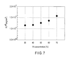
- FIG. 7 shows the Pd concentration dependence of the effective perpendicular magnetic anisotropy K u eff of a CoPd film used as the storage layer 3 .
- the horizontal axis indicates the Pd concentration, and the vertical axis indicates the effective magnetic anisotropy K u eff .
- a Pd concentration of 30 at % or more permits a high perpendicular magnetic anisotropy of 1 ⁇ 10 7 (erg/cm 3 ) or more.
- This high perpendicular magnetic anisotropy enables a magnetoresistive element showing high thermal stability to be provided despite miniaturization.
- the storage layer 3 may contain additional elements such as Fe, Ni, B, and V.
- the fixed layer 2 according to the first to sixth embodiments is described.
- the fixed layer 2 it is preferable to select a material and a multilayer film structure which do not easily change the magnetization direction, in contrast to the storage layer 3 . That is, it is preferable to select a material and a multilayer film structure which are high in effective magnetic anisotropy K u eff and saturation magnetization M S and which are high in magnetic relaxation constant ⁇ .
- the following materials are used for the third magnetic material film 2 d that constitutes the fixed layer 2 in the first to fourth embodiments.
- Artificial lattice includes a structure having alternately stacked layers of an alloy (magnetic layer) which includes at least one of Fe, Co, and Ni and an alloy (nonmagnetic layer) which includes at least one of Cr, Pt, Pd, Ag, Ir, Rh, Ru, Os, Re, Au, Cu, Gd, Tb, and Dy.
- such artificial lattice includes Co/Pt artificial lattice, Co/Pd artificial lattice, CoCr/Pt artificial lattice, Co/Ru artificial lattice, Co/Os artificial lattice, Co/Au artificial lattice, and Ni/Cu artificial lattice.
- Examples of an artificial lattice structure that uses two magnetic layers include Co/Ni artificial lattice and Fe/Ni artificial lattice.
- the effective magnetic anisotropy and the saturation magnetization of such artificial lattice can be adjusted by adjusting the addition of an element to the magnetic layer, the thickness ratio between the magnetic layer and the nonmagnetic layer, and the stacking period.
- Ordered alloys include an alloy which includes one or more of Fe, Co, and Ni and which include one or more of Pt and Pd.
- the crystal structure of this alloy is an L1 0 ordered alloy.
- the L1 0 ordered alloy includes, for example, Fe 50 Pt 50 , Fe 50 Pd 50 , Co 50 Pt 50 , Fe 30 Ni 20 Pt 50 , Co 30 Fe 20 Pt 50 , and Co 30 Ni 20 Pt 50 .
- the composition ratios in these ordered alloys are illustrative are not limited.
- the effective magnetic anisotropy and the saturation magnetization can be adjusted by adding, to these ordered alloys, an impurity element such as Cu, Cr, Ag, or B, or an alloy of these elements, or an insulator.
- an impurity element such as Cu, Cr, Ag, or B, or an alloy of these elements, or an insulator.
- Disordered alloys include a metal which includes cobalt (Co) as the main component and which includes one or more of Cr, Ta, Nb, V, W, Hf, Ti, Zr, Pt, Pd, B, Fe, and Ni.
- Co cobalt
- the disordered alloys include, for example, a CoCr alloy, a CoPt alloy, a CoCrPt alloy, a CoCrPtTa alloy, and a CoCrNb alloy.
- the effective magnetic anisotropy and the saturation magnetization of these alloys can be adjusted by changing the ratio of a nonmagnetic element.
- An alloy of a rare earth metal and a transition metal enables both a ferrimagnetic material and a ferromagnetic material to be obtained by the material of the rare earth metal.
- ferrimagnetic material examples include an alloy which includes Tb, Dy, or Gd, and an at least one of Fe, Co, and Ni.
- ferrimagnetic materials include, for example, TbFe, TbCo, TbFeCo, DyTbFeCo, and GdTbCo.
- the ferromagnetic material include an alloy which includes Sm, Nd, Ho, and at least one of Fe, Co, and Ni.
- Such ferromagnetic materials include, for example, SmCo 5 and NdFeB. The magnetic anisotropy and the saturation magnetization of these alloys can be adjusted by adjusting the composition ratio.
- the fixed layer 2 has a structure in which the first magnetic material film 2 a , the nonmagnetic material film 2 b , the second magnetic material film 2 c , and the third magnetic material film 2 d are stacked in this order from the side contacting the nonmagnetic layer 4 .
- the first magnetic material film 2 a is made of a material including at least one of Co, Fe, and Ni, or an alloy in which 0 to 30 at % of at least one of B, Al, and Si is added to the above material, or a multilayer film structure that includes the above materials.
- the nonmagnetic material film 2 b is made of a material comprising at least one of Ta, Zr, Nb, Mo, Ru, Ti, V, Cr, W, Hf, Pt, Pd, Rh, and Ir.
- the second magnetic material film 2 c is made of a material which includes Co as the main component and which may include, as an additional element, at least one of Fe, Ni, B, Al, Si, Ta, Zr, Nb, Mo, Ru, Ti, V, Cr, W, and Hf.
- the enlarged sectional view in FIG. 1 illustrates that the second magnetic material film 2 c is Co and the third magnetic material film 2 d is Co/Pt artificial lattice.
- the Co of second magnetic material film 2 c is thicker than the Co of the Co/Pt artificial lattice.
- the Co thickness of second magnetic material film 2 c is 7 ⁇
- the Co thickness of the Co/Pt artificial lattice is 3 ⁇
- the Pt thickness of the Co/Pt artificial lattice is 7 ⁇ .
- the Co thickness of the second magnetic material film 2 c , the Co thickness of the Co/Pt artificial lattice, and the Pt thickness of the Co/Pt artificial lattice are respectively not limited 7 ⁇ , 3 ⁇ , and 7 ⁇ .
- the Co thickness of second magnetic material film 2 c , the Co thickness of the Co/Pt artificial lattice, and the Pt thickness of the Co/Pt artificial lattice may respectively range from 4 ⁇ to 20 ⁇ , from 2 ⁇ to 8 ⁇ , and from 2 ⁇ to 15 ⁇ .
- the Co of the second magnetic material film 2 c is thicker than the Co of the Co/Pt artificial lattice.
- the fixed layer 2 can be thinner by adopting the Co/Pt artificial lattice with the smaller Co thickness than the Co thickness of the second magnetic material film 2 c .
- the thinner fixed layer 2 brings about the thinner bias layer (shift adjustment layer) 22 .
- the third magnetic material film 2 d may employ other artificial lattice except for the Co/Pt artificial lattice.
- the other artificial lattice is, for example, CoCr/Pt artificial lattice, Co/Ru artificial lattice, Co/Os artificial lattice, Co/Au artificial lattice, and Ni/Cu artificial lattice, Co/Ni artificial lattice, or Fe/Ni artificial lattice.
- the thickness of Co and the thickness of nonmagnetic metal are respectively 2 ⁇ -8 ⁇ , and 2 ⁇ -15 ⁇ as in the case of Co/Pt artificial lattice.
- the thickness of nonmagnetic metal is 2 ⁇ -15 ⁇ as in the case of Co/Pt artificial lattice.
- the Co concentration of the second magnetic material film 2 c is higher than the Co concentration of the first magnetic material film 2 a .
- the surface of the second magnetic material film 2 c where the second magnetic material film 2 c contacts the third magnetic material film 2 d is higher in Co concentration than the surface of the first magnetic material film 2 a where the nonmagnetic layer 4 contacts the first magnetic material film 2 a.
- FIG. 8A shows the dependence of the TMR ratio on the thickness of the second magnetic material film 2 c in the magnetoresistive element.
- Sample A is the magnetoresistive element in which the second magnetic material film 2 c is higher in Co concentration than the first magnetic material film 2 a .
- Sample B is the magnetoresistive element in which the second magnetic material film 2 c has the same Co concentration as the first magnetic material film 2 a.
- Sample A shows higher TMR ratio than Sample B at all thickness. That is, Sample A shows a TMR ratio of 120% and satisfactory characteristics at a thickness of 5 ⁇ to 30 ⁇ .
- Sample B the magnetization easy axis of the fixed layer 2 is in a in-plane direction when the thickness of the second magnetic material film 2 c is 13 ⁇ . Therefore, the antiparallel magnetization state is not obtained, and no TMR ratio is obtained. It is found out from magnetization curves that, in the whole thickness region of Sample A, the fixed layer 2 is magnetized in the direction perpendicular to the film plane even if no external magnetic field is applied thereto.
- FIG. 8B shows the change of the TMR ratio with the heat treatment temperature.
- the vertical axis indicates the TMR ratio after the heat treatment wherein the TMR ratio before the heat treatment is 1, and the horizontal axis indicates the heat treatment temperature.
- Samples a, b, and c are produced from Sample A by setting the thickness of the second magnetic material film 2 c to 13 ⁇ , 10 ⁇ , and 4 ⁇ , respectively.
- Sample d is produced from Sample B by setting the thickness of the second magnetic material film 2 c to 4 ⁇ .
- Sample c is greater than Samples a and b in the deterioration of the TMR ratio at 300° C. or more.
- the thickness of the second magnetic material film 2 c cannot be more than 20 ⁇ . It is thus preferable that the thickness of the second magnetic material film 2 c is more than 4 ⁇ and is 20 ⁇ or less.
- a stack structure in which the first magnetic material film 2 a , the nonmagnetic material film 2 b , and the second magnetic material film 2 c are stacked in this order from the side of the nonmagnetic layer 4 is shown as an experimental example.
- a stack structure having two or more magnetic material films and two or more nonmagnetic material films for example, a stack structure comprising the first magnetic material film 2 a , the nonmagnetic material film 2 b , the first magnetic material film 2 a , the nonmagnetic material film 2 b , and the second magnetic material film 2 c from the side of the nonmagnetic layer 4 , or a stack structure comprising the first magnetic material film 2 a , the nonmagnetic material film 2 b , the second magnetic material film 2 c , the nonmagnetic material film 2 b , and the second magnetic material film 2 c from the side of the nonmagnetic layer 4 .
- the concentration distributions and thickness of the first magnetic material film 2 a and the second magnetic material film 2 c that contain C can be identified by an analysis that uses electron energy loss spectroscopy (TEM-EELS) for a transmission electron microscope or secondary ion mass spectrometry (SIMS). Moreover, the concentration distributions and thickness can also be identified in the magnetoresistive element by using energy dispersive X-ray spectrometry (TEM-EDX).
- TEM-EELS electron energy loss spectroscopy
- SIMS secondary ion mass spectrometry
- concentration distributions and thickness can also be identified in the magnetoresistive element by using energy dispersive X-ray spectrometry (TEM-EDX).
- the constituent films other than a third magnetic material film 2 d have the above-mentioned materials and characteristics, so that similar advantageous effects can be expected.
- the interface magnetic film is the first magnetic material film 2 a that constitutes the fixed layer 2 in the first to sixth embodiments, and is the interface magnetic film 3 b that constitutes the storage layer 3 in the second and fourth to sixth embodiments.
- These interface magnetic films have a configuration in which magnetic material layers and nonmagnetic material layers are repeatedly stacked for one or more periods.
- the interface magnetic film is an alloy which includes at least one of Co, Fe, and Ni.
- oxides having an NaCl structure When oxides having an NaCl structure are used for the nonmagnetic layer 4 , the oxides having an NaCl structure allow a (100) face to be easily grown as a preferential orientation face if crystals of these oxides are grown
- the magnetic material layer contacting the nonmagnetic layer 4 is an alloy (Co 100-x Fe x ) 100-y B y (0 ⁇ y ⁇ 30 at %) which contains Co, Fe, and Ni.
- An element having a high melting point which includes at least one of Ta, W, Hf, Zr, Nb, Mo, Ti, V, and Cr, or an alloy of these elements is preferably used for the nonmagnetic material layer included in the interface magnetic film.
- Ta is used for the nonmagnetic material layer
- CoFeB is used for the magnetic material layer
- the distribution shows that the concentration of B is higher at points closer to the Ta layer because B in CoFeB of the magnetic material layer is drawn to Ta after the heat treatment.
- the interface magnetic film has a configuration in which magnetic material layers and nonmagnetic material layers are repeatedly stacked for one or more periods.
- the magnetic material layer preferably has magnetic exchange coupling via the nonmagnetic material layer, that the nonmagnetic material layer is preferably 10 ⁇ or less and particularly preferably 5 ⁇ or less. This permits the magnetization direction of the interface magnetic film to be aligned with the magnetization directions of the magnetic film 3 a and the magnetic film 2 a.
- the storage layer it is necessary to have a structure that allows an atom dense face to be easily oriented, in order to form a perpendicular magnetization film having a magnetization easy axis in the direction perpendicular to the film plane. That is, the crystal orientation needs to be controlled so that the (111) face of the face-centered cubic (FCC) structure and the (001) face of a hexagonal close-packed (HCP) structure are oriented. Therefore, the selection of an underlying layer material and a stack configuration is important.
- FCC face-centered cubic
- HCP hexagonal close-packed
- FIG. 9 is a sectional view of a stack structure comprising the underlying layer 5 and the storage layer 3 in the magnetoresistive element according to the embodiment.
- Ta having a thickness of about 5 nm is provided as a contact layer 8 between a lower electrode 7 and the underlying layer 5 .
- the underlying layer 5 has a stack structure in which underlying films 5 a , 5 b , and 5 c are stacked in this order.
- a CoPd layer having a thickness of about 2 nm is provided as the storage layer 3 on the underlying layer 5 .
- the configuration above the storage layer 3 is as shown in FIG. 1 to FIG. 6 .
- the underlying film 5 c included in the underlying layer 5 is preferably made of a metal material that lattice-matches the storage layer 3 .
- the underlying film 5 a preferably include a material and a configuration that allow the underlying films 5 b and 5 c to be smooth and to be improved in crystal orientation.
- the underlying films 5 b and 5 c are preferably made of a Ru layer having a thickness of about 3 nm and a Pt layer having a thickness of about 3 nm, respectively.
- a metal having a dense structure is used as the underlying film 5 c .
- Metals which lattice-match the storage layer 3 include, for example, Pt, Pd, Ir, and Ru.
- a CoPd alloy or a CoPt alloy and which have a close-packed structure include, for example, Pt, Pd, Ir, and Ru.
- an alloy comprising two metal elements such as Pt—Pd or Pt—Ir or three or more metal elements may be used.
- alloys of the above-mentioned metals and fcc metals such as Cu, Au, and Al: Pt—Cu, Pd—Cu, Ir—Cu, Pt—Au, Ru—Au, Pt—Al, and Ir—Al, or to use alloys of Re, Ti, Zr, and Hf and hcp metals: Pt—Re, Pt—Ti, Ru—Re, Ru—Ti, Ru—Zr, and Ru—Hf.
- the thickness range of the underlying layer 5 is preferably 30 nm or less.
- the underlying films 5 b and 5 c are stacked in order to stack materials having different lattice constants so that the lattice constant is adjusted before the formation of a CoPd alloy or a CoPt alloy. For example, if Ru is formed for the underlying film 5 b and Pt is formed for the underlying film 5 c , Pt of the underlying film 5 c will have a lattice constant different from a bulk lattice constant due to Ru of the underlying film 5 b . However, as described above, the lattice constant can be adjusted even when an alloy is used. Therefore, one of the underlying films 5 b and 5 c can be omitted.
- the underlying film 5 a is used to improve smoothness and to improve the crystal orientation of the metals of the underlying films 5 b and 5 c having close-packed structures. More specifically, Ta, for example, is used for the underlying film 5 a . If the thickness of the underlying film 5 a is too large, it takes a long time to form the underlying film 5 a , leading to lower productivity. If the thickness of the underlying film 5 a is too small, the above-mentioned effect of controlling orientation is lost. It is therefore preferable that the thickness of the underlying film 5 a ranges from 1 nm to 10 nm.
- the material of the nonmagnetic layer 4 in the first to sixth embodiments is preferably an oxide having an NaCl structure.
- Such an oxide includes, for example, MgO, CaO, SrO, TiO, VO, and NbO. These oxides having an NaCl structure allow a (100) face to be easily grown as a preferential orientation face if crystals of these oxides are grown
- the (100) face can be extremely easily preferentially oriented on a CoFeX (X represents at least one of the elements B, C, and N) amorphous alloy to which B, C, or N is added.
- X represents at least one of the elements B, C, and N
- the magnetoresistive element increases in conductivity and decreases in resistance value.
- the formation of the ⁇ 1 band is the point in developing a high TMR ratio.
- the interfaces between the (100) face of the nonmagnetic layer 4 made of an oxide having an NaCl structure and the storage layer 3 as well as the fixed layer 2 have to be well consistent.
- the storage layer and the fixed layer have stack structures as described above to further improve the lattice match in the (100) face of the nonmagnetic layer 4 made of an oxide layer having an NaCl structure. From the viewpoint of forming the ⁇ 1 band, it is preferable that such materials that the lattice mismatch in the (100) face of the nonmagnetic layer 4 is 5% or less are selected as the interface magnetic film 3 b that constitutes the storage layer 3 and the interface magnetic film 2 a that constitutes the fixed layer 2 .
- the nonmagnetic layer 21 and the bias layer (shift adjustment layer) 22 may be disposed between the fixed layer 2 and the cap layer 6 . This makes it possible to lessen and adjust of the shift of a switching current of the storage layer 3 resulting from the leakage magnetic field from the fixed layer 2 .
- the nonmagnetic layer 21 has thermal resistance that prevents the fixed layer 2 and the bias layer 22 from being mixed by a thermal process and also has a function to control crystal orientation during the formation of the bias layer 22 .
- the thickness of the nonmagnetic layer 21 is 5 nm or less.
- the bias layer 22 is made of a ferromagnetic body having a magnetization easy axis in the direction perpendicular to the film plane. More specifically, the materials listed for the fixed layer 2 can be used. However, as the bias layer 22 is farther from the storage layer 3 than the fixed layer 2 , the thickness or the saturation magnetization Ms of the bias layer 22 needs to be set to be more than that of the fixed layer 2 so that the leakage magnetic field applied to the storage layer 3 is adjusted by the bias layer 22 .
- Equation ( 2 ) below needs to be satisfied M S2 ⁇ t 2 ⁇ M S22 ⁇ t 22 (2) wherein t 2 and M S2 are the thickness or the saturation magnetization of the fixed layer 2 , and t 22 and M S22 are the thickness or the saturation magnetization of the bias layer 22 .
- the element is fabricated into a size of 50 nm.
- a magnetic material having a saturation magnetization M S of 1000 emu/cm 3 and a thickness of 5 nm is used for the fixed layer 2 to offset the shift of the switching current.
- the required characteristics are as follows:
- the thickness of the nonmagnetic layer 21 is 3 nm.
- the saturation magnetization M S of the bias layer 22 is 1000 emu/cm 3 .
- the thickness of the bias layer 22 is about 15 nm.
- the magnetization directions of the fixed layer 2 and the bias layer 22 need to be set to be antiparallel to each other.
- the coercive force H c2 of the fixed layer 2 and the coercive force H c22 of the bias layer 22 satisfy the relation H c2 >H c22 or H c2 ⁇ H c22 .
- the magnetization directions of the fixed layer 2 and the bias layer 22 can be set to be antiparallel to each other by switching the magnetization direction of the layer lower in coercive force by minor loop magnetization in advance.
- the magnetization directions of the fixed layer 2 and the bias layer 22 can also be set to be antiparallel to each other by the synthetic anti-ferromagnetic (SAF) coupling of the fixed layer 2 and the bias layer 22 via the nonmagnetic layer 21 .
- SAF synthetic anti-ferromagnetic
- Ru for example, is used as the material of the nonmagnetic layer 21 so that the magnetization directions of the fixed layer 2 and the bias layer 22 can also be coupled to be antiparallel to each other.
- the magnetic field leaking from the fixed layer 2 can be reduced by the bias layer 22 , so that the shift of the switching current of the storage layer 3 can be reduced.
- element-to-element variation of the switching current of the storage layer 3 can also be reduced.
- the nonmagnetic layer 21 and the bias layer 22 are disposed between the fixed layer 2 and the cap layer 6 in the example described above, the nonmagnetic layer and the bias layer (shift adjustment layer) may be disposed between the storage layer 3 and the underlying layer 5 . In this case, the shift of the switching current of the storage layer 3 resulting from the leakage magnetic field from the fixed layer 2 can be lessened and adjusted.
- the nonmagnetic layers and the bias layers (shift adjustment layers) may be disposed between the fixed layer 2 and the cap layer 6 and between the storage layer 3 and the underlying layer 5 .
- the Co concentration of the second magnetic material film 2 c included in the fixed layer 2 is higher than the Co concentration of the first magnetic material film 2 a , and the thickness of the second magnetic material film 2 c is larger, so that it is possible to provide a magnetoresistive element which shows only a slight change in electric characteristics in response to a heat treatment after film formation and which has high thermal resistance. That is, it is possible to provide a magnetoresistive element for the spin transfer torque writing method which is thermally stable and which can inhibit the decrease of the magnetoresistance ratio.
- a magnetic random access memory (MRAM) according to the seventh embodiment is described with reference to FIG. 10 and FIG. 11 .
- the MRAM according to the seventh embodiment is configured to use the magnetoresistive element according to one of the first to sixth embodiments as a storage element.
- the magnetoresistive element 1 according to the first embodiment is used as a magnetoresistive element.
- FIG. 10 is a circuit diagram showing the configuration of the MRAM according to the seventh embodiment.
- the MRAM according to the seventh embodiment includes a memory cell array 40 having memory cells MC arranged in matrix form. Pairs of bit lines BL,/BL are provided in the memory cell array 40 to extend in a column direction. Word lines WL are also provided in the memory cell array 40 to extend in a row direction.
- a memory cell MC is located at the intersection of the bit line BL and the word line WL.
- Each memory cell MC includes the magnetoresistive element 1 and a select transistor (e.g. n-channel MOS transistor) 41 .
- One end of the magnetoresistive element 1 is connected to the bit line BL.
- the other end of the magnetoresistive element 1 is connected to the drain terminal of the select transistor 41 .
- the source terminal of the select transistor 41 is connected to the bit line/BL.
- the gate terminal of the select transistor 41 is connected to the word line WL.
- a row decoder 42 is connected to the word line WL.
- a write circuit 44 and a read circuit 45 are connected to the pairs of bit lines BL,/BL.
- a column decoder 43 is connected to the write circuit 44 and the read circuit 45 .
- Each memory cell MC is selected by the row decoder 42 and the column decoder 43 .
- Data is written into the memory cell MC as follows. First, in order to select a memory cell MC to write data into, the word line WL connected to this memory cell MC is activated. As a result, the select transistor 41 is turned on.
- a bi-directional write current Iw is supplied to the magnetoresistive element 1 in accordance with the data to be written. More specifically, when the write current Iw is supplied to the magnetoresistive element 1 from left to right, the write circuit 44 applies a positive voltage to the bit line BL, and applies a ground voltage to the bit line/BL. When the write current Iw is supplied to the magnetoresistive element 1 from right to left, the write circuit 44 applies a positive voltage to the bit line/BL, and applies a ground voltage to the bit line BL. In this way, data “0” or data “1” can be written into the memory cell MC.
- Data is read from the memory cell MC as follows. First, the select transistor 41 of a memory cell MC to be selected is turned on.
- the read circuit 45 supplies the magnetoresistive element 1 with, for example, a read current Ir running from right to left, that is, supplies the read current Ir from the bit line/BL to the bit line BL.
- the read circuit 45 detects the resistance value of the magnetoresistive element 1 in accordance with the read current Ir. Further, the read circuit 45 reads data stored in the magnetoresistive element 1 from the detected resistance value.
- FIG. 11 is a sectional view showing the structure of one memory cell MC.
- the memory cell MC has the magnetoresistive element (MTJ) 1 and the select transistor 41 .
- An element isolation insulating layer 46 is provided in the surface area of a p-type semiconductor substrate 51 .
- the surface area of the semiconductor substrate 51 in which the element isolation insulating layer 46 is not provided is an element area (active area) in which elements are formed.
- the element isolation insulating layer 46 includes, for example, shallow trench isolation (STI).
- STI shallow trench isolation
- silicon oxide is used for the STI.
- a source area S and a drain area D that are separated from each other are formed in the element area of the semiconductor substrate 51 .
- the source area S and the drain area D include n+ type diffusion areas formed by introducing a high-concentration impurity, for example, an n+ type impurity into the semiconductor substrate 51 .
- a gate insulating film 41 A is formed on the semiconductor substrate 51 between the source area S and the drain area D.
- a gate electrode 41 B is formed on the gate insulating film 41 A. This gate electrode 41 B functions as the word line WL.
- the select transistor 41 is provided on the semiconductor substrate 51 .
- a interconnect layer 53 is formed on the source area S via a contact 52 .
- the interconnect layer 53 functions as the bit line/BL.
- a leader line 55 is formed above the drain area D via a contact 54 .
- the magnetoresistive element 1 intervening between a lower electrode 7 and an upper electrode 9 is provided above the leader line 55 .
- a interconnect layer 56 is formed on the upper electrode 9 .
- the interconnect layer 56 functions as the bit line BL.
- the space between the semiconductor substrate 51 and the interconnect layer 56 is filled with an interlayer insulating film 57 made of, for example, silicon oxide.
- an MRAM can be configured by using the magnetoresistive element 1 .
- the magnetoresistive element 1 can be used not only as a magnetic memory of a spin transfer torque writing type but also as a magnetic domain wall motion magnetic memory.
- the MRAM shown in the seventh embodiment is applicable to various devices. Several applications of the MRAM are described below.
- FIG. 12 shows an extracted DSL data path unit of a digital subscriber line (DSL) modem.
- DSL digital subscriber line
- This modem includes, for example, a programmable digital signal processor (DSP) 100 , an analog-digital (A/D) converter 110 , a digital-analog (D/A) converter 120 , a transmission driver 130 , and a receiver amplifier 140 .
- DSP programmable digital signal processor
- A/D analog-digital
- D/A digital-analog
- a band pass filter is not shown in FIG. 12 .
- an MRAM 170 according to the seventh embodiment and an electrically erasable and programmable ROM (EEPROM) 180 are shown as various types of optional memories for holding a line code program (program which is executed by the DSP and which selects and operates the modem in accordance with, for example, coded subscriber's line information and transmission conditions (line code: QAM, CAP, RSK, FM, AM, PAM, or DWMT)).
- line code program program which is executed by the DSP and which selects and operates the modem in accordance with, for example, coded subscriber's line information and transmission conditions (line code: QAM, CAP, RSK, FM, AM, PAM, or DWMT)).
- the MRAM 170 and the EEPROM 180 are used as the memories for holding the line code program in this application, the EEPROM 180 may be replaced by an MRAM. That is, the MRAM alone may be used instead of using two kinds of memories.
- FIG. 13 shows a mobile telephone terminal 300 as another application.
- a communication section 200 that enables a communication function includes, for example, a sending/receiving antenna 201 , an antenna duplexer 202 , a receiver 203 , a baseband processor 204 , a digital signal processor (DSP) 205 used as an audio codec, a speaker (receiver) 206 , a microphone (transmitter) 207 , a transmitter 208 , and a frequency synthesizer 209 .
- DSP digital signal processor
- the mobile telephone terminal 300 is also provided with a control section 220 for controlling the components of the mobile telephone terminal 300 .
- the control section 220 is a microcomputer which is formed by connecting a CPU 221 , a ROM 222 , an MRAM 223 according to the seventh embodiment, and a flash memory 224 via a bus 225 .
- Programs to be executed by the CPU 221 and necessary display data such as fonts are stored in the ROM 222 in advance.
- the MRAM 223 is mainly used as a work area, and is used by the CPU 221 to store, as needed, data being calculated during the execution of the program, or used to temporarily store data exchanged between the control section 220 and each component.
- the flash memory 224 is used to store setting parameters so that even if the mobile telephone terminal 300 is powered off, conditions set immediately before the power-off are stored to enable the same setting when the mobile telephone terminal 300 is powered on next. This prevents the disappearance of the stored setting parameters even if the mobile telephone terminal 300 is powered off.
- the mobile telephone terminal 300 is also provided with an audio data reproduction processor 211 , an external output terminal 212 , an LCD controller 213 , a liquid crystal display (LCD) 214 for display, and a ringer 215 which generates a ringing tone.
- an audio data reproduction processor 211 an external output terminal 212 , an LCD controller 213 , a liquid crystal display (LCD) 214 for display, and a ringer 215 which generates a ringing tone.
- LCD liquid crystal display
- the audio data reproduction processor 211 reproduces audio data input to the mobile telephone terminal 300 (or audio information (audio data) stored in a later-described external memory 240 ).
- the reproduced audio data (audio information) can be transmitted to a headphone or a mobile speaker via the external output terminal 212 and thereby taken out.
- the audio information can be reproduced by providing the audio data reproduction processor 211 .
- the LCD controller 213 receives, for example, display information from the CPU 221 via the bus 225 , converts the display information to LCD control information for controlling the LCD 214 , and drives the LCD 214 to display the information.
- the mobile telephone terminal 300 is provided with interface circuits (I/F) 231 , 233 , and 235 , the external memory 240 , an external memory slot 232 , a key operation unit 234 , and an external input/output terminal 236 .
- the external memory 240 for example, a memory card is inserted into the external memory slot 232 .
- the external memory slot 232 is connected to the bus 225 via the interface circuit (I/F) 231 .
- the slot 232 is thus provided in the mobile telephone terminal 300 such that information in the mobile telephone terminal 300 can be written into the external memory 240 or information (e.g. audio information) stored in the external memory 240 can be input to the mobile telephone terminal 300 .
- the key operation unit 234 is connected to the bus 225 via the interface circuit (I/F) 233 . Key input information input from the key operation unit 234 is transmitted to, for example, the CPU 221 .
- the external input/output terminal 236 is connected to the bus 225 via the interface circuit (I/F) 235 .
- the external input/output terminal 236 functions as a terminal for inputting various kinds of information to the mobile telephone terminal 300 from the outside or outputting information from the mobile telephone terminal 300 to the outside.
- the flash memory 224 may be replaced by an MRAM, and the ROM 222 can also be replaced by an MRAM.
- FIG. 14 to FIG. 18 respectively show examples of how the MRAM is applied to cards (MRAM cards) such as smart media for storing media content.
- an MRAM card body 400 has an MRAM chip 401 therein.
- the card body 400 has an opening 402 formed in a position corresponding to the MRAM chip 401 so that the MRAM chip 401 is exposed.
- This opening 402 is provided with a shutter 403 so that the MRAM chip 401 is protected by the shutter 403 when the MRAM card is carried.
- the shutter 403 is made of a material such as ceramics having the effect of blocking an external magnetic field.
- the shutter 403 is opened to expose the MRAM chip 401 .
- An external terminal 404 takes out content data stored in the MRAM card.
- FIG. 15 and FIG. 16 show a card insertion type transfer device for transferring data to the MRAM card.
- a data transfer device 500 has a storage portion 500 a .
- a first MRAM card 550 is stored in the storage portion 500 a .
- the storage portion 500 a is provided with an external terminal 530 which is electrically connected to the first MRAM card 550 . This external terminal 530 is used to rewrite data in the first MRAM card 550 .
- a second MRAM card 450 used by an end user is inserted from an insertion portion 510 of the data transfer device 500 as indicated by an arrow, and pushed in until stopped by a stopper 520 .
- This stopper 520 also serves as a member to align the first MRAM card 550 with the second MRAM card 450 .
- a control signal is supplied to the external terminal 530 from a first MRAM data rewrite controller, and data stored in the first MRAM card 550 is transferred to the second MRAM card 450 .
- FIG. 17 is a sectional view showing a fit type transfer device for transferring data to the MRAM card.
- a transfer device 600 is a type that mounts the second MRAM card 450 on the first MRAM card 550 in a fitting manner using the stopper 520 as a mark, as indicated by an arrow.
- the transfer method is the same as that of the card insertion type and is therefore not described.
- FIG. 18 is a sectional view showing a slide type transfer device for transferring data to the MRAM card.
- a transfer device 700 is provided with a tray slide 560 as in a CD-ROM drive or a DVD drive. This tray slide 560 moves as indicated by an arrow. When the tray slide 560 has moved to the position indicated by a broken line, the second MRAM card 450 is mounted on the tray slide 560 , and the tray slide 560 then moves to convey the second MRAM card 450 into the transfer device 700 .
- the slide type transfer device is the same as the card insertion type transfer device in that the second MRAM card 450 is conveyed so that the tip of the second MRAM card 450 comes into contact with the stopper 520 , and in the transfer method. Therefore, no explanations are given in these respects.
- the MRAM described in the seventh embodiment can be used in a file memory capable of high-speed random writing, a mobile terminal capable of high-speed downloading, a mobile player capable of high-speed downloading, a semiconductor memory for broadcasting devices, a drive recorder, a home video, a high-capacity buffer memory for communication, and a semiconductor memory for a security camera, thus providing many industrial advantages.
- a magnetoresistive element for the spin transfer torque writing method which is thermally stable and which can inhibit the decrease of the magnetoresistance ratio, and also provide a magnetic memory that uses such a magnetoresistive element.
Landscapes
- Mram Or Spin Memory Techniques (AREA)
- Hall/Mr Elements (AREA)
Abstract
Description
Δ=K u eff ·V/(k B T)=(K u−2πNM S 2)·Va/(k B T) (1)
M S2 ×t 2 <M S22 ×t 22 (2)
wherein t2 and MS2 are the thickness or the saturation magnetization of the fixed
Claims (19)
Priority Applications (2)
| Application Number | Priority Date | Filing Date | Title |
|---|---|---|---|
| US14/152,286 US8946837B2 (en) | 2011-07-04 | 2014-01-10 | Semiconductor storage device with magnetoresistive element |
| US14/573,231 US9312477B2 (en) | 2011-07-04 | 2014-12-17 | Semiconductor storage device with magnetoresistive element |
Applications Claiming Priority (4)
| Application Number | Priority Date | Filing Date | Title |
|---|---|---|---|
| JP2011148444A JP5728311B2 (en) | 2011-07-04 | 2011-07-04 | Magnetoresistive element and magnetic memory |
| JP2011-148444 | 2011-07-04 | ||
| US13/424,136 US8659103B2 (en) | 2011-07-04 | 2012-03-19 | Magnetoresistive element and magnetic memory using the same |
| US14/152,286 US8946837B2 (en) | 2011-07-04 | 2014-01-10 | Semiconductor storage device with magnetoresistive element |
Related Parent Applications (1)
| Application Number | Title | Priority Date | Filing Date |
|---|---|---|---|
| US13/424,136 Continuation-In-Part US8659103B2 (en) | 2011-07-04 | 2012-03-19 | Magnetoresistive element and magnetic memory using the same |
Related Child Applications (1)
| Application Number | Title | Priority Date | Filing Date |
|---|---|---|---|
| US14/573,231 Continuation US9312477B2 (en) | 2011-07-04 | 2014-12-17 | Semiconductor storage device with magnetoresistive element |
Publications (2)
| Publication Number | Publication Date |
|---|---|
| US20140124884A1 US20140124884A1 (en) | 2014-05-08 |
| US8946837B2 true US8946837B2 (en) | 2015-02-03 |
Family
ID=50621578
Family Applications (2)
| Application Number | Title | Priority Date | Filing Date |
|---|---|---|---|
| US14/152,286 Active US8946837B2 (en) | 2011-07-04 | 2014-01-10 | Semiconductor storage device with magnetoresistive element |
| US14/573,231 Active US9312477B2 (en) | 2011-07-04 | 2014-12-17 | Semiconductor storage device with magnetoresistive element |
Family Applications After (1)
| Application Number | Title | Priority Date | Filing Date |
|---|---|---|---|
| US14/573,231 Active US9312477B2 (en) | 2011-07-04 | 2014-12-17 | Semiconductor storage device with magnetoresistive element |
Country Status (1)
| Country | Link |
|---|---|
| US (2) | US8946837B2 (en) |
Cited By (5)
| Publication number | Priority date | Publication date | Assignee | Title |
|---|---|---|---|---|
| US9231192B2 (en) | 2011-02-28 | 2016-01-05 | Kabushiki Kaisha Toshiba | Semiconductor memory device and method for manufacturing the same |
| US9373776B2 (en) | 2011-07-04 | 2016-06-21 | Kabushiki Kaisha Toshiba | Magnetoresistive element and magnetic memory using the same |
| US20170047375A1 (en) * | 2015-08-11 | 2017-02-16 | Kabushiki Kaisha Toshiba | Magnetoresistive memory device and manufacturing method of the same |
| US9837468B2 (en) | 2015-10-15 | 2017-12-05 | Samsung Electronics Co., Ltd. | Magnetoresistive random access memory device and method of manufacturing the same |
| US20190207085A1 (en) * | 2017-12-29 | 2019-07-04 | Spin Memory, Inc. | Magnetic Memory having a Pinning Synthetic Antiferromagnetic Structure (SAF) with Cobalt over Platinum (Pt/Co) Bilayers |
Families Citing this family (7)
| Publication number | Priority date | Publication date | Assignee | Title |
|---|---|---|---|---|
| US8946837B2 (en) | 2011-07-04 | 2015-02-03 | Kabushiki Kaisha Toshiba | Semiconductor storage device with magnetoresistive element |
| JP2014072393A (en) * | 2012-09-28 | 2014-04-21 | Sony Corp | Storage element, storage device, magnetic head |
| JP6427396B2 (en) | 2014-11-19 | 2018-11-21 | 株式会社東芝 | Magnetoresistance element and magnetic memory |
| DE112016002318B4 (en) * | 2015-05-22 | 2021-01-14 | Canon Anelva Corporation | Magnetoresistance effect device |
| WO2017010549A1 (en) * | 2015-07-16 | 2017-01-19 | 国立大学法人東北大学 | Magnetoresistive element and magnetic memory |
| WO2019125366A1 (en) * | 2017-12-18 | 2019-06-27 | Intel Corporation | Spin orbit coupling based memory with resistivity modulation |
| JP2020035975A (en) * | 2018-08-31 | 2020-03-05 | キオクシア株式会社 | Magnetic storage device |
Citations (32)
| Publication number | Priority date | Publication date | Assignee | Title |
|---|---|---|---|---|
| US20020044479A1 (en) | 2000-10-13 | 2002-04-18 | Takashi Ikeda | Magnetoresistive element, and magnetic memory using the same |
| US20040100855A1 (en) * | 2002-11-22 | 2004-05-27 | Kabushiki Kaisha Toshiba | Magneto-resistance effect element, magnetic memory and magnetic head |
| US6816347B2 (en) | 1999-12-28 | 2004-11-09 | Kabushiki Kaisha Toshiba | Magnetoresistive element and magnetic recording apparatus |
| US20060114714A1 (en) | 2004-11-29 | 2006-06-01 | Yoshiharu Kanegae | Magnetroresistive random access memory and method of manufacturing the same |
| US20070206333A1 (en) | 2006-02-14 | 2007-09-06 | Hitachi Global Storage Technologies Netherlands B.V. | Magnetoresistive head and a manufacturing method thereof |
| JP2008252018A (en) | 2007-03-30 | 2008-10-16 | Toshiba Corp | Magnetoresistance effect element, and magnetic random access memory using the same |
| US20090080238A1 (en) | 2007-09-25 | 2009-03-26 | Kabushiki Kaisha Toshiba | Magnetoresistive element and magnetoresistive random access memory including the same |
| US20090080239A1 (en) | 2007-09-26 | 2009-03-26 | Toshihiko Nagase | Magnetoresistive element and magnetic memory |
| US20090141410A1 (en) | 2007-12-03 | 2009-06-04 | Fujitsu Limited | Current-perpendicular-to-the-plane structure magnetoresistive element and method of making the same and storage apparatus |
| JP2009239052A (en) | 2008-03-27 | 2009-10-15 | Toshiba Corp | Magnetoresistance element and magnetic memory |
| JP2010010720A (en) | 2009-10-13 | 2010-01-14 | Toshiba Corp | Magnetoresistance effect element and magnetic random access memory utilizing the same |
| JP2010016408A (en) | 2009-10-19 | 2010-01-21 | Toshiba Corp | Magnetoresistive element and magnetic memory |
| US7663197B2 (en) | 2005-10-19 | 2010-02-16 | Kabushiki Kaisha Toshiba | Magnetoresistive element |
| US20100096716A1 (en) * | 2007-02-12 | 2010-04-22 | Yadav Technology Inc. | Spin-transfer torque magnetic random access memory having magnetic tunnel junction with perpendicular magnetic anisotropy |
| JP2010232499A (en) | 2009-03-27 | 2010-10-14 | Toshiba Corp | Magnetoresistive element and magnetic memory |
| WO2010137679A1 (en) | 2009-05-28 | 2010-12-02 | 株式会社日立製作所 | Magneto-resistance effect element and random access memory using same |
| US20110007560A1 (en) | 2009-05-27 | 2011-01-13 | Commissariat A L'energie Atomique Et Aux Energies Alternatives | Spin polarised magnetic device |
| WO2011036795A1 (en) | 2009-09-28 | 2011-03-31 | 株式会社 東芝 | Magnetoresistive effect element and magnetic memory |
| US20110073970A1 (en) | 2009-09-25 | 2011-03-31 | Tadashi Kai | Magnetoresistive element and magnetic memory |
| US20110116305A1 (en) | 2005-06-23 | 2011-05-19 | Makoto Nagamine | Magnetoresistive element |
| US20120068284A1 (en) | 2010-09-17 | 2012-03-22 | Kabushiki Kaisha Toshiba | Magnetoresistive effect element and magnetic memory |
| US20120069640A1 (en) | 2010-09-16 | 2012-03-22 | Kabushiki Kaisha Toshiba | Magnetoresistive element and magnetic memory |
| US20120068285A1 (en) | 2010-09-17 | 2012-03-22 | Kabushiki Kaisha Toshiba | Magnetoresistive effect element, magnetic memory, and method of manufacturing magnetoresistive effect element |
| US20120217476A1 (en) | 2011-02-28 | 2012-08-30 | Kabushiki Kaisha Toshiba | Semiconductor memory device and method for manufacturing the same |
| US20120241881A1 (en) | 2011-03-25 | 2012-09-27 | Tohoku University | Magnetoresistive element and magnetic memory |
| US8299552B2 (en) | 2007-09-26 | 2012-10-30 | Kabushiki Kaisha Toshiba | Magnetoresistive element and magnetic memory |
| US8305801B2 (en) | 2010-09-16 | 2012-11-06 | Kabushiki Kaisha Toshiba | Magnetoresistive element and magnetic memory |
| US20120294079A1 (en) | 2011-05-19 | 2012-11-22 | Sony Corporation | Memory element and memory device |
| US20130001713A1 (en) | 2011-06-30 | 2013-01-03 | Kabushiki Kaisha Toshiba | Magnetoresistive element and magnetic memory using the same |
| US20130001714A1 (en) | 2011-06-30 | 2013-01-03 | Kabushiki Kaisha Toshiba | Magnetoresistive element and magnetic memory |
| US20130009259A1 (en) | 2011-07-04 | 2013-01-10 | Kabushiki Kaisha Toshiba | Magnetoresistive element and magnetic memory using the same |
| US8670268B2 (en) | 2011-07-04 | 2014-03-11 | Kabushiki Kaisha Toshiba | Magnetoresistive element and magnetic memory using the same |
Family Cites Families (4)
| Publication number | Priority date | Publication date | Assignee | Title |
|---|---|---|---|---|
| KR20080029819A (en) | 2006-09-29 | 2008-04-03 | 가부시끼가이샤 도시바 | Magnetoresistive effect device and magnetic random access memory using the same |
| JP2008109118A (en) | 2006-09-29 | 2008-05-08 | Toshiba Corp | Magnetoresistance effect element and magnetic random access memory using it |
| JP2012099741A (en) | 2010-11-04 | 2012-05-24 | Toshiba Corp | Magnetic random access memory and method of manufacturing the same |
| US8946837B2 (en) | 2011-07-04 | 2015-02-03 | Kabushiki Kaisha Toshiba | Semiconductor storage device with magnetoresistive element |
-
2014
- 2014-01-10 US US14/152,286 patent/US8946837B2/en active Active
- 2014-12-17 US US14/573,231 patent/US9312477B2/en active Active
Patent Citations (53)
| Publication number | Priority date | Publication date | Assignee | Title |
|---|---|---|---|---|
| US6816347B2 (en) | 1999-12-28 | 2004-11-09 | Kabushiki Kaisha Toshiba | Magnetoresistive element and magnetic recording apparatus |
| JP2002124716A (en) | 2000-10-13 | 2002-04-26 | Canon Inc | Magnetoresistance element and memory element using the element |
| US20020044479A1 (en) | 2000-10-13 | 2002-04-18 | Takashi Ikeda | Magnetoresistive element, and magnetic memory using the same |
| US20040100855A1 (en) * | 2002-11-22 | 2004-05-27 | Kabushiki Kaisha Toshiba | Magneto-resistance effect element, magnetic memory and magnetic head |
| US20060114714A1 (en) | 2004-11-29 | 2006-06-01 | Yoshiharu Kanegae | Magnetroresistive random access memory and method of manufacturing the same |
| US20110116305A1 (en) | 2005-06-23 | 2011-05-19 | Makoto Nagamine | Magnetoresistive element |
| US8036025B2 (en) | 2005-10-19 | 2011-10-11 | Kabushiki Kaisha Toshiba | Magnetoresistive element |
| US7663197B2 (en) | 2005-10-19 | 2010-02-16 | Kabushiki Kaisha Toshiba | Magnetoresistive element |
| US20120008381A1 (en) | 2005-10-19 | 2012-01-12 | Toshihiko Nagase | Magnetoresistive element |
| US20070206333A1 (en) | 2006-02-14 | 2007-09-06 | Hitachi Global Storage Technologies Netherlands B.V. | Magnetoresistive head and a manufacturing method thereof |
| US20100096716A1 (en) * | 2007-02-12 | 2010-04-22 | Yadav Technology Inc. | Spin-transfer torque magnetic random access memory having magnetic tunnel junction with perpendicular magnetic anisotropy |
| US20080253174A1 (en) | 2007-03-30 | 2008-10-16 | Masatoshi Yoshikawa | Magnetoresistance effect element and magnetoresistive random access memory using the same |
| JP2008252018A (en) | 2007-03-30 | 2008-10-16 | Toshiba Corp | Magnetoresistance effect element, and magnetic random access memory using the same |
| US7924607B2 (en) | 2007-03-30 | 2011-04-12 | Kabushiki Kaisha Toshiba | Magnetoresistance effect element and magnetoresistive random access memory using the same |
| US7768824B2 (en) | 2007-09-25 | 2010-08-03 | Kabushiki Kaisha Toshiba | Magnetoresistive element and magnetoresistive random access memory including the same |
| US20100230770A1 (en) | 2007-09-25 | 2010-09-16 | Kabushiki Kaisha Toshiba | Magnetoresistive element and magnetoresistive random access memory including the same |
| JP2009081216A (en) | 2007-09-25 | 2009-04-16 | Toshiba Corp | Magnetoresistance effect element and magnetic random access memory using the same |
| US20110222335A1 (en) | 2007-09-25 | 2011-09-15 | Kabushiki Kaisha Toshiba | Magnetoresistive element and magnetoresistive random access memory including the same |
| US20110211389A1 (en) | 2007-09-25 | 2011-09-01 | Kabushiki Kaisha Toshiba | Magnetoresistive element and magnetoresistive random access memory including the same |
| US20090080238A1 (en) | 2007-09-25 | 2009-03-26 | Kabushiki Kaisha Toshiba | Magnetoresistive element and magnetoresistive random access memory including the same |
| US8098514B2 (en) * | 2007-09-26 | 2012-01-17 | Kabushiki Kaisha Toshiba | Magnetoresistive element and magnetic memory |
| US8299552B2 (en) | 2007-09-26 | 2012-10-30 | Kabushiki Kaisha Toshiba | Magnetoresistive element and magnetic memory |
| JP2009081315A (en) | 2007-09-26 | 2009-04-16 | Toshiba Corp | Magnetoresistive element, and magnetic memory |
| US20090080239A1 (en) | 2007-09-26 | 2009-03-26 | Toshihiko Nagase | Magnetoresistive element and magnetic memory |
| US20090141410A1 (en) | 2007-12-03 | 2009-06-04 | Fujitsu Limited | Current-perpendicular-to-the-plane structure magnetoresistive element and method of making the same and storage apparatus |
| JP2009239052A (en) | 2008-03-27 | 2009-10-15 | Toshiba Corp | Magnetoresistance element and magnetic memory |
| US20120088125A1 (en) | 2009-03-27 | 2012-04-12 | National University Corporation Tohoku University | Magnetoresistive element and magnetic memory |
| JP2010232499A (en) | 2009-03-27 | 2010-10-14 | Toshiba Corp | Magnetoresistive element and magnetic memory |
| US20110007560A1 (en) | 2009-05-27 | 2011-01-13 | Commissariat A L'energie Atomique Et Aux Energies Alternatives | Spin polarised magnetic device |
| WO2010137679A1 (en) | 2009-05-28 | 2010-12-02 | 株式会社日立製作所 | Magneto-resistance effect element and random access memory using same |
| US20110073970A1 (en) | 2009-09-25 | 2011-03-31 | Tadashi Kai | Magnetoresistive element and magnetic memory |
| JP2011071352A (en) | 2009-09-25 | 2011-04-07 | Toshiba Corp | Magnetoresistive element and magnetic memory |
| US20120099369A1 (en) | 2009-09-25 | 2012-04-26 | Tadashi Kai | Magnetoresistive element and magnetic memory |
| WO2011036795A1 (en) | 2009-09-28 | 2011-03-31 | 株式会社 東芝 | Magnetoresistive effect element and magnetic memory |
| US20120243305A1 (en) | 2009-09-28 | 2012-09-27 | Masahiko Nakayama | Magnetoresistance effect element and magnetic memory |
| JP2010010720A (en) | 2009-10-13 | 2010-01-14 | Toshiba Corp | Magnetoresistance effect element and magnetic random access memory utilizing the same |
| JP2010016408A (en) | 2009-10-19 | 2010-01-21 | Toshiba Corp | Magnetoresistive element and magnetic memory |
| US20120069640A1 (en) | 2010-09-16 | 2012-03-22 | Kabushiki Kaisha Toshiba | Magnetoresistive element and magnetic memory |
| US8305801B2 (en) | 2010-09-16 | 2012-11-06 | Kabushiki Kaisha Toshiba | Magnetoresistive element and magnetic memory |
| US20120068285A1 (en) | 2010-09-17 | 2012-03-22 | Kabushiki Kaisha Toshiba | Magnetoresistive effect element, magnetic memory, and method of manufacturing magnetoresistive effect element |
| US20120068284A1 (en) | 2010-09-17 | 2012-03-22 | Kabushiki Kaisha Toshiba | Magnetoresistive effect element and magnetic memory |
| US20120217476A1 (en) | 2011-02-28 | 2012-08-30 | Kabushiki Kaisha Toshiba | Semiconductor memory device and method for manufacturing the same |
| US8653614B2 (en) | 2011-02-28 | 2014-02-18 | Kabushiki Kaisha Toshiba | Semiconductor memory device and method for manufacturing the same |
| US20140117478A1 (en) | 2011-02-28 | 2014-05-01 | Kabushiki Kaisha Toshiba | Semiconductor memory device and method for manufacturing the same |
| US20120241881A1 (en) | 2011-03-25 | 2012-09-27 | Tohoku University | Magnetoresistive element and magnetic memory |
| US20120294079A1 (en) | 2011-05-19 | 2012-11-22 | Sony Corporation | Memory element and memory device |
| JP2012243933A (en) | 2011-05-19 | 2012-12-10 | Sony Corp | Storage element and storage device |
| US20130001713A1 (en) | 2011-06-30 | 2013-01-03 | Kabushiki Kaisha Toshiba | Magnetoresistive element and magnetic memory using the same |
| US20130001714A1 (en) | 2011-06-30 | 2013-01-03 | Kabushiki Kaisha Toshiba | Magnetoresistive element and magnetic memory |
| US20130009259A1 (en) | 2011-07-04 | 2013-01-10 | Kabushiki Kaisha Toshiba | Magnetoresistive element and magnetic memory using the same |
| US8659103B2 (en) | 2011-07-04 | 2014-02-25 | Kabushiki Kaisha Toshiba | Magnetoresistive element and magnetic memory using the same |
| US8670268B2 (en) | 2011-07-04 | 2014-03-11 | Kabushiki Kaisha Toshiba | Magnetoresistive element and magnetic memory using the same |
| US20140131823A1 (en) | 2011-07-04 | 2014-05-15 | Kabushiki Kaisha Toshiba | Magnetoresistive element and magnetic memory using the same |
Non-Patent Citations (13)
| Title |
|---|
| Background Art Information (Concise Explanation for JP 2009-81216), Toshiba, Jan. 19, 2011. |
| Background Art Information, Toshiba, Dec. 8, 2011. |
| Ikeda et al., "A Perpedicular-Anisotrophy CoFeB-MgO Magnetic Tunnel Junction", Nature Materials, 2804 pp. 1-3 Jul. 2010. |
| Japanese Office Action dated Oct. 14, 2014 for JP Application No. 2011-148444 filed Jul. 4, 2011. |
| U.S. Appl. No. 13/049,806, filed Mar. 16, 2011, Yamakawa. |
| U.S. Appl. No. 13/233,906, filed Sep. 15, 2011, Nagase. |
| U.S. Appl. No. 13/407,630, filed Feb. 28, 2012, Ikeno et al. |
| U.S. Appl. No. 13/424,136, filed Mar. 19, 2012, Watanabe et al. |
| U.S. Appl. No. 13/427,732, filed Mar. 22, 2012, Nagase. |
| U.S. Appl. No. 13/432,626, filed Mar. 28, 2012, Nakayama. |
| U.S. Appl. No. 14/147,903, filed Jan. 6, 2014, Ikeno et al. |
| U.S. Appl. No. 14/159,057, filed Jan. 20, 2014, Nagase. |
| Worledge, D.C., et al. "Spin torque switching of perpendicular Ta|CoFeB|MgO-based magnetic tunnel junctions", Applied Physics Letters 98, 022501 (2011), in 3 pages. |
Cited By (8)
| Publication number | Priority date | Publication date | Assignee | Title |
|---|---|---|---|---|
| US9231192B2 (en) | 2011-02-28 | 2016-01-05 | Kabushiki Kaisha Toshiba | Semiconductor memory device and method for manufacturing the same |
| US9373776B2 (en) | 2011-07-04 | 2016-06-21 | Kabushiki Kaisha Toshiba | Magnetoresistive element and magnetic memory using the same |
| US20170047375A1 (en) * | 2015-08-11 | 2017-02-16 | Kabushiki Kaisha Toshiba | Magnetoresistive memory device and manufacturing method of the same |
| US10043852B2 (en) * | 2015-08-11 | 2018-08-07 | Toshiba Memory Corporation | Magnetoresistive memory device and manufacturing method of the same |
| US9837468B2 (en) | 2015-10-15 | 2017-12-05 | Samsung Electronics Co., Ltd. | Magnetoresistive random access memory device and method of manufacturing the same |
| US10096650B2 (en) | 2015-10-15 | 2018-10-09 | Samsung Electronics Co., Ltd. | Method of manufacturing magnetoresistive random access memory device |
| US20190207085A1 (en) * | 2017-12-29 | 2019-07-04 | Spin Memory, Inc. | Magnetic Memory having a Pinning Synthetic Antiferromagnetic Structure (SAF) with Cobalt over Platinum (Pt/Co) Bilayers |
| US10388853B2 (en) * | 2017-12-29 | 2019-08-20 | Spin Memory, Inc. | Magnetic memory having a pinning synthetic antiferromagnetic structure (SAF) with cobalt over platinum (Pt/Co) bilayers |
Also Published As
| Publication number | Publication date |
|---|---|
| US20140124884A1 (en) | 2014-05-08 |
| US20150171317A1 (en) | 2015-06-18 |
| US9312477B2 (en) | 2016-04-12 |
Similar Documents
| Publication | Publication Date | Title |
|---|---|---|
| US9312477B2 (en) | Semiconductor storage device with magnetoresistive element | |
| US8659103B2 (en) | Magnetoresistive element and magnetic memory using the same | |
| JP4599425B2 (en) | Magnetoresistive element and magnetic memory | |
| US8705269B2 (en) | Magnetoresistive element and magnetic memory | |
| US9373776B2 (en) | Magnetoresistive element and magnetic memory using the same | |
| US8665639B2 (en) | Magnetoresistive element and magnetic memory | |
| JP5072120B2 (en) | Magnetoresistive element and magnetic memory | |
| US9153770B2 (en) | Magnetoresistive element and magnetic memory | |
| US9018719B2 (en) | Magnetoresistive element and magnetic memory | |
| JP5010565B2 (en) | Magnetoresistive element and magnetic memory | |
| US9312475B2 (en) | Magnetoresistive element, magnetic memory, and method of manufacturing magnetoresistive element | |
| US8669628B2 (en) | Magnetoresistive element and magnetic memory using the same |
Legal Events
| Date | Code | Title | Description |
|---|---|---|---|
| AS | Assignment |
Owner name: KABUSHIKI KAISHA TOSHIBA, JAPAN Free format text: ASSIGNMENT OF ASSIGNORS INTEREST;ASSIGNORS:WATANABE, DAISUKE;NISHIYAMA, KATSUYA;NAGASE, TOSHIHIKO;AND OTHERS;SIGNING DATES FROM 20120412 TO 20120515;REEL/FRAME:031941/0512 |
|
| AS | Assignment |
Owner name: KABUSHIKI KAISHA TOSHIBA, JAPAN Free format text: ASSIGNMENT OF ASSIGNORS INTEREST;ASSIGNORS:WATANABE, DAISUKE;NISHIYAMA, KATSUYA;NAGASE, TOSHIHIKO;AND OTHERS;SIGNING DATES FROM 20140225 TO 20140403;REEL/FRAME:033480/0383 |
|
| STCF | Information on status: patent grant |
Free format text: PATENTED CASE |
|
| MAFP | Maintenance fee payment |
Free format text: PAYMENT OF MAINTENANCE FEE, 4TH YEAR, LARGE ENTITY (ORIGINAL EVENT CODE: M1551) Year of fee payment: 4 |
|
| AS | Assignment |
Owner name: TOSHIBA MEMORY CORPORATION, JAPAN Free format text: DE-MERGER;ASSIGNOR:KABUSHIKI KAISHA TOSHIBA;REEL/FRAME:051260/0291 Effective date: 20170401 Owner name: KIOXIA CORPORATION, JAPAN Free format text: CHANGE OF NAME AND ADDRESS;ASSIGNOR:TOSHIBA MEMORY CORPORATION;REEL/FRAME:051262/0881 Effective date: 20191001 Owner name: TOSHIBA MEMORY CORPORATION, JAPAN Free format text: MERGER;ASSIGNORS:TOSHIBA MEMORY CORPORATION;K.K PANGEA;REEL/FRAME:051262/0776 Effective date: 20180801 |
|
| MAFP | Maintenance fee payment |
Free format text: PAYMENT OF MAINTENANCE FEE, 8TH YEAR, LARGE ENTITY (ORIGINAL EVENT CODE: M1552); ENTITY STATUS OF PATENT OWNER: LARGE ENTITY Year of fee payment: 8 |