JP2008231218A - Phosphor material and white light-emitting diode - Google Patents
Phosphor material and white light-emitting diode Download PDFInfo
- Publication number
- JP2008231218A JP2008231218A JP2007071818A JP2007071818A JP2008231218A JP 2008231218 A JP2008231218 A JP 2008231218A JP 2007071818 A JP2007071818 A JP 2007071818A JP 2007071818 A JP2007071818 A JP 2007071818A JP 2008231218 A JP2008231218 A JP 2008231218A
- Authority
- JP
- Japan
- Prior art keywords
- light
- phosphor material
- excitation
- polycrystal
- fluorescence
- Prior art date
- Legal status (The legal status is an assumption and is not a legal conclusion. Google has not performed a legal analysis and makes no representation as to the accuracy of the status listed.)
- Pending
Links
Images


Classifications
-
- Y—GENERAL TAGGING OF NEW TECHNOLOGICAL DEVELOPMENTS; GENERAL TAGGING OF CROSS-SECTIONAL TECHNOLOGIES SPANNING OVER SEVERAL SECTIONS OF THE IPC; TECHNICAL SUBJECTS COVERED BY FORMER USPC CROSS-REFERENCE ART COLLECTIONS [XRACs] AND DIGESTS
- Y02—TECHNOLOGIES OR APPLICATIONS FOR MITIGATION OR ADAPTATION AGAINST CLIMATE CHANGE
- Y02B—CLIMATE CHANGE MITIGATION TECHNOLOGIES RELATED TO BUILDINGS, e.g. HOUSING, HOUSE APPLIANCES OR RELATED END-USER APPLICATIONS
- Y02B20/00—Energy efficient lighting technologies, e.g. halogen lamps or gas discharge lamps
Abstract
Description
本発明は、蛍光体材料に関するものであり、詳細には、励起光により蛍光を発し、透過励起光と蛍光の合成により白色光などを発光することができる蛍光体材料及びそれを用いた白色LEDに関するものである。 The present invention relates to a phosphor material, and more specifically, a phosphor material capable of emitting fluorescence by excitation light and emitting white light by synthesizing transmitted excitation light and fluorescence, and a white LED using the phosphor material It is about.
青色LED(Light Emitting Diode)チップと、青色LEDチップから発せられた青色光線によって黄色に発光するYAG蛍光体を組合せた白色LEDが開発されている(特許文献1)。この白色LEDは、従来の照明装置等の光源に比べ、長寿命、低消費電力、環境負荷物質を含まない等の利点を有しているため、白熱電球や蛍光灯に替わる次世代の光源として期待されている。 A white LED that combines a blue LED (Light Emitting Diode) chip and a YAG phosphor that emits yellow light by blue light emitted from the blue LED chip has been developed (Patent Document 1). This white LED has advantages such as long life, low power consumption, and no inclusion of environmentally hazardous substances, as compared to conventional light sources such as lighting devices, so it can be used as a next-generation light source to replace incandescent bulbs and fluorescent lamps. Expected.
しかしながら、特許文献1に開示されている白色LEDは、蛍光体が粉末状態であるため、透明樹脂に混合して励起用LED上に設ける構造を有している。このため、LEDチップから発せられる熱あるいは光によって透明樹脂が劣化し、変色を引き起こす。その結果、発光強度の低下や色度ずれが起こり、LEDの寿命が短くなるという問題がある。このような問題を解消するため、透明樹脂に変えてガラスを用い、ガラスマトリックス中に蛍光体となる結晶を保持する構造が考えられる。このような構造によれば、LEDチップから発せられる熱による劣化を抑制することができる。しかしながら、発光効率が市販の白色LEDに比べて低くなるという課題がある。
However, the white LED disclosed in
また、市販の白色LEDは、上述のような青色LEDの上に黄色発光する蛍光体を設けた構造を有しているが、得られる白色光の色調が中心部分と端部分で異なる、いわゆる配光特性が悪いといった問題も有している。これは、LEDチップの上に設けられる蛍光体の厚みのばらつきや、蛍光体を塗り付ける部分の形状が影響していると考えられる。このような配光特性を改善する方法として、蛍光体を分散している樹脂中に光を散乱させる散乱剤を混入させたり、あるいは蛍光体に濃度分布をつけるなどの方法が考えられるが、コスト面で高くなる。 Further, a commercially available white LED has a structure in which a phosphor emitting yellow light is provided on a blue LED as described above, but the so-called arrangement in which the color tone of the obtained white light is different between the central portion and the end portion. There is also a problem that optical characteristics are poor. This is considered to be due to the variation in the thickness of the phosphor provided on the LED chip and the shape of the portion to which the phosphor is applied. As a method for improving such a light distribution characteristic, a method of mixing a scattering agent that scatters light in a resin in which a phosphor is dispersed or a concentration distribution on the phosphor can be considered. In terms of height.
本発明は、後述するようにセラミックからなる蛍光体材料を用いるものである。特許文献2においては、セラミックからなる蛍光体材料を用い、波長変換層をこの蛍光体材料から形成することが開示されている。しかしながら、この従来技術に開示されているセラミックからなる波長変換層は、入射した光を波長変換して出射することを目的とするものであり、本発明のように光を透過させる性質と光を散乱させる性質の両方を有する半透明の多結晶体ではない。
本発明の目的は、蛍光体を励起するための励起光と、蛍光体から発せられる蛍光とが均質に混合された光を発することができる蛍光体材料及びそれを用いた白色LEDを提供することにある。 An object of the present invention is to provide a phosphor material capable of emitting light in which excitation light for exciting a phosphor and fluorescence emitted from the phosphor are homogeneously mixed, and a white LED using the phosphor material. It is in.
本発明の蛍光体材料は、光を透過させる性質と光を散乱させる性質の両方を有し、波長550nmにおける散乱係数が10〜700cm−1である半透明の多結晶体からなり、可視光からなる励起光を照射すると、その励起光の一部を吸収し励起光とは異なる波長域の蛍光を発し、多結晶体内部で励起光と蛍光とが散乱を繰り返すことにより、励起光が照射される励起面と反対側の発光面から励起光と蛍光とが均質に混合された光を発することを特徴としている。 The phosphor material of the present invention has both a property of transmitting light and a property of scattering light, and is composed of a translucent polycrystalline body having a scattering coefficient of 10 to 700 cm −1 at a wavelength of 550 nm, and from visible light. When the excitation light is irradiated, a part of the excitation light is absorbed and fluorescence in a wavelength region different from that of the excitation light is emitted, and the excitation light and the fluorescence are scattered inside the polycrystal to be irradiated with the excitation light. It is characterized by emitting light in which excitation light and fluorescence are uniformly mixed from a light emitting surface opposite to the excitation surface.
本発明の蛍光体材料は、光を透過させる性質と光を散乱させる性質の両方を有し、波長550nmにおける散乱係数が10〜700cm−1である半透明の多結晶体からなる。このため、可視光からなる励起光を照射すると、その励起光の一部は、多結晶体中を透過して、励起光が照射される励起面と反対側の発光面から出射される。また、励起光の一部は吸収されて、励起光と異なる波長域の蛍光を発する。また、多結晶体内部では、上記の励起光と蛍光とが散乱を繰り返すことにより、励起光が照射される励起面と反対側の発光面から励起光と蛍光とが均質に混合された光が発光される。従って、本発明によれば、蛍光体を励起するための励起光と蛍光体から発射される蛍光とが均質に混合された光を発する蛍光体材料とすることができる。 The phosphor material of the present invention comprises a translucent polycrystal having both a property of transmitting light and a property of scattering light, and a scattering coefficient of 10 to 700 cm −1 at a wavelength of 550 nm. For this reason, when excitation light composed of visible light is irradiated, a part of the excitation light is transmitted through the polycrystalline body and emitted from the light emitting surface opposite to the excitation surface irradiated with the excitation light. Further, part of the excitation light is absorbed and emits fluorescence in a wavelength region different from that of the excitation light. In addition, inside the polycrystal, the excitation light and the fluorescence are repeatedly scattered, so that the light in which the excitation light and the fluorescence are homogeneously mixed from the light emitting surface opposite to the excitation surface irradiated with the excitation light. Emits light. Therefore, according to the present invention, a phosphor material that emits light in which excitation light for exciting the phosphor and fluorescence emitted from the phosphor are homogeneously mixed can be obtained.
本発明の蛍光体材料は、波長550nmにおける散乱係数が10〜700cm−1であることを特徴としている。この散乱係数は、半透明の多結晶体における光を透過させる性質と光を散乱させる性質の度合を示す指標である。散乱係数が10cm−1よりも小さいと、励起光が多結晶体中を吸収或いは反射されることなく直進する確率が高くなり、結果として、発光面から発せられる光に中心部と周辺部で色度に差が生じ、配光性が悪くなる。また、散乱係数が700cm−1よりも大きいと、光散乱による損失が大きくなり、得られる光の強度が小さくなる。散乱係数が10〜700cm−1の範囲内にあることにより、励起光及び蛍光が多結晶体内部で適度に散乱し、両者が均質に混合される。その結果、配光性に優れた色むらの無い発光を得ることができる。散乱係数は、より好ましくは20〜500cm−1の範囲であり、さらに好ましくは50〜400cm−1の範囲であり、特に好ましくは、100〜300cm−1の範囲である。なお、散乱係数μは、以下の式によって定義され、式中、Lはサンプルの厚さ(cm)であり、Tは透過率、Rは反射率を表す。 The phosphor material of the present invention is characterized in that the scattering coefficient at a wavelength of 550 nm is 10 to 700 cm −1 . This scattering coefficient is an index indicating the degree of the property of transmitting light and the property of scattering light in the translucent polycrystalline body. When the scattering coefficient is smaller than 10 cm −1, the probability that the excitation light travels straight without being absorbed or reflected in the polycrystalline body is increased, and as a result, the color emitted from the light emitting surface is colored in the central portion and the peripheral portion. A difference occurs in the degree, resulting in poor light distribution. On the other hand, if the scattering coefficient is larger than 700 cm −1, the loss due to light scattering increases and the intensity of the obtained light decreases. When the scattering coefficient is in the range of 10 to 700 cm −1 , excitation light and fluorescence are appropriately scattered inside the polycrystalline body, and both are uniformly mixed. As a result, light emission with excellent color distribution and no color unevenness can be obtained. Scattering coefficient is more preferably within a range of 20~500Cm -1, more preferably in the range of 50~400Cm -1, particularly preferably in the range of 100~300cm -1. The scattering coefficient μ is defined by the following equation, where L is the thickness (cm) of the sample, T is the transmittance, and R is the reflectance.
μ=−(1/L)×ln(T/(1−R)2)
本発明において、多結晶体における微結晶粒子の大きさは、10〜100μmの範囲内にあることが好ましい。多結晶体における結晶粒子径を10〜100μmの範囲内にすることにより、励起光とその励起光によって発する蛍光を微結晶界面で多重反射させ、より効果的に散乱させることができる。微結晶粒子の粒子径が10μmより小さいと、光の散乱量が大きくなりすぎ、得られる光の強度が低下する。また、微結晶の粒子径が100μmよりも大きいと、励起光の蛍光体材料中の直線透過性が増加し、色度にばらつきが生じる。
μ = − (1 / L) × ln (T / (1-R) 2 )
In the present invention, the size of the microcrystalline particles in the polycrystal is preferably in the range of 10 to 100 μm. By setting the crystal particle diameter in the polycrystal within the range of 10 to 100 μm, the excitation light and the fluorescence emitted by the excitation light can be multiple-reflected at the microcrystal interface and scattered more effectively. When the particle diameter of the microcrystalline particles is smaller than 10 μm, the amount of light scattering becomes too large, and the intensity of the obtained light is lowered. On the other hand, when the particle diameter of the microcrystal is larger than 100 μm, the linear transmittance of the excitation light in the phosphor material increases, and the chromaticity varies.
本発明における散乱係数は、結晶粒子径の大きさによって制御することが可能である。結晶粒子径が大きくなると、光を散乱させるための結晶粒子界面の面積が小さくなるため、光を透過させる性質が大きくなり、光を散乱させる性質が小さくなる。その結果、散乱係数が小さくなり、発光強度は高くなるが、配光性が低下する。 The scattering coefficient in the present invention can be controlled by the size of the crystal particle diameter. As the crystal particle diameter increases, the area of the crystal particle interface for scattering light decreases, so that the property of transmitting light increases and the property of scattering light decreases. As a result, the scattering coefficient is reduced and the light emission intensity is increased, but the light distribution is lowered.
結晶粒子径が小さくなると、光散乱をさせるための結晶粒子界面の面積が大きくなるため、光を散乱させる性質が大きくなり、光を透過させる性質が小さくなる。その結果、散乱係数が大きくなり、発光強度が低くなる。 As the crystal particle diameter decreases, the area of the crystal particle interface for light scattering increases, so that the property of scattering light increases and the property of transmitting light decreases. As a result, the scattering coefficient increases and the emission intensity decreases.
多結晶体における微結晶粒子の結晶粒子径の範囲は、さらに好ましくは、15〜70μmであり、特に好ましくは、20〜50μmである。 The range of the crystal particle diameter of the microcrystalline particles in the polycrystal is more preferably 15 to 70 μm, and particularly preferably 20 to 50 μm.
多結晶体における微結晶粒子の大きさは、電子顕微鏡観察により平均値として測定することができる。 The size of the microcrystalline particles in the polycrystal can be measured as an average value by observation with an electron microscope.
また、多結晶体における微結晶粒子の粒子径は、材料を焼成して部材にする際の焼成温度及び焼成時間を調整することにより制御することができる。焼成温度が高くなるほど、結晶粒子径は大きくなり、逆に焼成温度が低くなるほど結晶粒子径は小さくなる。また、焼成時間が長くなるほど結晶粒子は大きくなり、逆に焼成時間が短くなるほど、結晶粒子径は小さくなる。 The particle diameter of the microcrystalline particles in the polycrystal can be controlled by adjusting the firing temperature and firing time when firing the material into a member. The higher the firing temperature, the larger the crystal particle size, and conversely, the lower the firing temperature, the smaller the crystal particle size. Further, the longer the firing time, the larger the crystal particles, and conversely, the shorter the firing time, the smaller the crystal particle diameter.
本発明において、多結晶体は、波長400〜500nmの光を吸収し、波長450〜780nmの光の蛍光を発する性質を有するものであることが好ましい。より好ましくは、青色の光を吸収し、黄色の蛍光を発する性質を有することが好ましい。このような多結晶体を用いることにより、多結晶体から発光する光と多結晶体中を透過する励起光とが合成されて、白色光を発することができる。なお、青色光とは、波長430〜480nmに中心波長を有する光を意味し、黄色光とは、波長535〜590nmに中心波長を有する光を意味する。 In the present invention, the polycrystalline body preferably has a property of absorbing light having a wavelength of 400 to 500 nm and emitting fluorescence of light having a wavelength of 450 to 780 nm. More preferably, it has a property of absorbing blue light and emitting yellow fluorescence. By using such a polycrystal, the light emitted from the polycrystal and the excitation light transmitted through the polycrystal are synthesized, and white light can be emitted. Blue light means light having a central wavelength at a wavelength of 430 to 480 nm, and yellow light means light having a central wavelength at a wavelength of 535 to 590 nm.
本発明における多結晶体は、ガーネット結晶中にCe3+を含む微結晶からなることが好ましい。ガーネット結晶中にCe3+を含む構造とすることにより、Ce3+が発光中心となり、青色の励起光を吸収し、黄色の蛍光を発せることができる。 The polycrystal in the present invention is preferably composed of a microcrystal containing Ce 3+ in a garnet crystal. By adopting a structure containing Ce 3+ in the garnet crystal, Ce 3+ becomes the emission center, absorbs blue excitation light, and can emit yellow fluorescence.
多結晶体中のCe2O3の濃度は、0.001〜0.5モル%であることが好ましい。Ce2O3の含有量が少なくなると、Ce3+から発せられる黄色の蛍光強度が弱くなり、白色光が得られにくくなる。一方、Ce2O3の含有量が多くなると、励起青色光の光のほとんどが吸収され、黄色の蛍光のみが得られるため、白色光が得られにくくなる。Ce2O3の含有量のさらに好ましい範囲は、0.002〜0.2モル%であり、特に好ましくは、0.005〜0.1モル%の範囲である。 The concentration of Ce 2 O 3 in the polycrystal is preferably 0.001 to 0.5 mol%. When the content of Ce 2 O 3 is reduced, the intensity of yellow fluorescence emitted from Ce 3+ becomes weak and it becomes difficult to obtain white light. On the other hand, when the content of Ce 2 O 3 is increased, most of the excitation blue light is absorbed and only yellow fluorescence is obtained, so that it is difficult to obtain white light. The more preferable range of the content of Ce 2 O 3 is 0.002 to 0.2 mol%, and particularly preferably 0.005 to 0.1 mol%.
なお、ガーネット結晶とは、一般的にはA3B2C3O12で表される結晶(A=Mg、Mn、Fe、Ca、Y、Gd等:B=Al、Cr、Fe、Ga、Sc等:C=Al、Si、Ga、Ge等)であり、上記したガーネット結晶として、特に、YAG結晶(Y3Al5O12結晶)またはYAG結晶固溶体であると、所望の黄色の蛍光を発するため好ましい。YAG結晶固溶体としては、Yの一部をGd、Sc、Ca及びMgからなる群から選択された少なくとも1種の元素で、及び/またはAlの一部をGa、Si、Ge及びScからなる群から選択された少なくとも1種の元素で置換したYAG結晶固溶体であってもよい。 The garnet crystal is generally a crystal represented by A 3 B 2 C 3 O 12 (A = Mg, Mn, Fe, Ca, Y, Gd, etc .: B = Al, Cr, Fe, Ga, Sc, etc .: C = Al, Si, Ga, Ge, etc.) As the above-mentioned garnet crystal, particularly a YAG crystal (Y 3 Al 5 O 12 crystal) or a YAG crystal solid solution, a desired yellow fluorescence can be obtained. It is preferable because it emits light. As a YAG crystal solid solution, a part of Y is at least one element selected from the group consisting of Gd, Sc, Ca and Mg, and / or a part of Al is a group consisting of Ga, Si, Ge and Sc. YAG crystal solid solution substituted with at least one element selected from
上記の蛍光体材料を得るには、まず、A3B2C3O12(A=Mg、Ca、Y、Gd等:B=Al、Ga、Sc等:C=Al、Si、Ga、Ge等)の量論組成となるように、高純度かつ数μm以下の粒径を有するA,BおよびCの酸化物原料を秤量し、これにCe2O3を0.001〜0.5モル%添加する。次にボールミル等により十分攪拌混合した後、得られた粉体を150〜250MPaの圧力でプレス成形する。続いて、得られた成形体を1500℃〜1800℃の温度で焼成する。この際、昇温過程の一部において1000Pa以下の減圧雰囲気中で焼成する。このようにすることで、上記のような波長400〜500nmの光を吸収し、波長450〜780nmの光の蛍光を発する性質を有する蛍光体材料を得ることができる。 To obtain the phosphor material, first, A 3 B 2 C 3 O 12 (A = Mg, Ca, Y, Gd, etc .: B = Al, Ga, Sc, etc .: C = Al, Si, Ga, Ge, etc.) Etc.), A, B and C oxide raw materials having a high purity and a particle size of several μm or less are weighed, and Ce 2 O 3 is added in an amount of 0.001 to 0.5 mol. %Added. Next, after sufficiently stirring and mixing with a ball mill or the like, the obtained powder is press-molded at a pressure of 150 to 250 MPa. Subsequently, the obtained molded body is fired at a temperature of 1500 ° C. to 1800 ° C. At this time, firing is performed in a reduced pressure atmosphere of 1000 Pa or less in a part of the temperature raising process. By doing so, it is possible to obtain a phosphor material having a property of absorbing light having a wavelength of 400 to 500 nm as described above and emitting fluorescence of light having a wavelength of 450 to 780 nm.
本発明における蛍光体材料、すなわち多結晶体は、任意の形状を有していてもよく、例えば、円盤状、柱状、棒状等の形状を有していてもよい。このような形状は、蛍光体材料を切断及び研磨加工等することにより形成することができる。 The phosphor material in the present invention, that is, the polycrystalline body, may have an arbitrary shape, for example, a disk shape, a columnar shape, a rod shape, or the like. Such a shape can be formed by cutting and polishing the phosphor material.
本発明における蛍光体材料、すなわち多結晶体は、上記のように任意の形状を有していてもよいものであるが、特に板状形状であることが好ましい。その理由は、蛍光体材料が板状であると、厚みを全体に均一にし易くなるため、励起光が入射し、励起にされた際、得られる色度に分布が生じにくくなるからである。 The phosphor material in the present invention, that is, the polycrystalline body may have an arbitrary shape as described above, but it is particularly preferable to have a plate shape. The reason is that if the phosphor material is plate-like, the thickness can be easily made uniform throughout, so that when the excitation light is incident and excited, the resulting chromaticity is less likely to be distributed.
本発明の蛍光体材料を板状にした場合の厚みは、0.01〜1.0mmであることが好ましい。蛍光体材料の厚みが薄くなりすぎると、蛍光体材料中の結晶量が少なくなり、例えば黄色の蛍光強度が弱くなり、白色光が得られなくなる場合がある。また、厚みが厚くなりすぎると、例えば、青色の励起光が吸収され透過しにくくなり、結果として、白色光を発する蛍光体材料が得にくくなるからである。蛍光体材料を板状とした場合の厚みのさらに好ましい範囲は、0.05〜0.8mmであり、特に好ましくは0.1〜0.5mmの範囲である。 The thickness when the phosphor material of the present invention is plate-shaped is preferably 0.01 to 1.0 mm. If the thickness of the phosphor material is too thin, the amount of crystals in the phosphor material is reduced, for example, the yellow fluorescence intensity becomes weak, and white light may not be obtained. Moreover, if the thickness is too thick, for example, blue excitation light is hardly absorbed and transmitted, and as a result, it is difficult to obtain a phosphor material that emits white light. A more preferable range of the thickness when the phosphor material is plate-shaped is 0.05 to 0.8 mm, particularly preferably 0.1 to 0.5 mm.
本発明の白色LEDは、上記本発明の蛍光体材料を用いたことを特徴としている。具体的には、蛍光体材料に励起光を照射するための励起光の光源と、本発明の蛍光体材料とを備えている。具体的には、励起光の光源として、青色LED素子などを備えている。白色LEDにおいては、蛍光体材料に入射した青色光の一部が蛍光体によって黄色の蛍光に波長変換され、また、残部の青色光が透過する。この波長変換された黄色光と、蛍光体材料中を透過した青色光とが合わさって、白色調に近いスペクトルを合成することにより、青色光を白色光に変換することができる。 The white LED of the present invention is characterized by using the phosphor material of the present invention. Specifically, a light source of excitation light for irradiating the phosphor material with excitation light and the phosphor material of the present invention are provided. Specifically, a blue LED element or the like is provided as a light source for excitation light. In the white LED, part of the blue light incident on the phosphor material is wavelength-converted to yellow fluorescence by the phosphor, and the remaining blue light is transmitted. By combining the wavelength-converted yellow light and the blue light transmitted through the phosphor material to synthesize a spectrum close to white tone, the blue light can be converted into white light.
本発明によれば、蛍光体を励起するための励起光と蛍光体から発せられる蛍光とが均質に混合された光を発する蛍光体材料とすることができる。本発明の蛍光体材料は、従来の波長変換部材のように樹脂材料をマトリックスとするものでないため、樹脂の劣化による発光強度の低下や短寿命化を抑制することができ、高い発光強度を有し、発光配光性に優れた蛍光体材料とすることができる。 ADVANTAGE OF THE INVENTION According to this invention, it can be set as the fluorescent substance material which emits the light with which the excitation light for exciting a fluorescent substance and the fluorescence emitted from a fluorescent substance were mixed uniformly. Since the phosphor material of the present invention does not use a resin material as a matrix unlike the conventional wavelength conversion member, it can suppress a decrease in emission intensity and a shortened life due to deterioration of the resin, and has a high emission intensity. And it can be set as the fluorescent material excellent in light emission light distribution.
また、本発明の白色LEDは、本発明の蛍光体材料を用いるものであるので、発光強度の低下や短寿命化を抑制することができ、高い発光強度で、発光配光性に優れた白色LEDとすることができる。 In addition, since the white LED of the present invention uses the phosphor material of the present invention, it is possible to suppress a decrease in light emission intensity and a shortened life, and a white light having high light emission intensity and excellent light emission light distribution. It can be an LED.
本発明の蛍光体材料及び白色LEDは、配光性に優れ、高強度で発光することができるものであるので、照明、ディスプレイ等の発光装置、自動車等の前照光の光源に用いる材料として好適なものである。 Since the phosphor material and the white LED of the present invention are excellent in light distribution and can emit light with high intensity, they are suitable as materials used for light sources for lighting, displays and the like, and light sources for headlights such as automobiles. It is a thing.
以下、本発明を具体的な実施例により説明するが、本発明は以下の実施例に限定されるものではない。 Hereinafter, the present invention will be described with reference to specific examples, but the present invention is not limited to the following examples.
(実施例1〜10及び比較例11〜12)
蛍光体材料を以下のようにして焼成し、作製した。
(Examples 1-10 and Comparative Examples 11-12)
The phosphor material was fired and manufactured as follows.
まず、表1及び表2に示す組成となるように、高純度かつ2μm以下の粒子径を有する酸化物原料を秤量した。秤量した酸化物原料に対して、焼結助剤としてテトラエトキシシランをそれぞれ0.6重量%となるように添加した。次に、エタノール中でアルミナボールミルを用い、17時間撹拌混合した。その後、減圧雰囲気で粉体を乾燥し、得られた粉体を200MPaの圧力でプレス成形してプレス成形体を得た。次に、このプレス成形体を、表1及び表2に示すそれぞれの焼成条件で焼成した。なお、昇温速度は、1000℃まで10℃/分とし、1000℃からは昇温速度を5℃/分とした。表1及び表2に示す焼成条件の温度を最高温度とし、この最高温度を表1及び表2に示す時間保持した後、5℃/分の降温速度で室温まで冷却した。温度プロファイルを図7に示す。 First, oxide raw materials having high purity and a particle diameter of 2 μm or less were weighed so as to have the compositions shown in Tables 1 and 2. Tetraethoxysilane was added as a sintering aid to the weighed oxide raw materials so that each amount would be 0.6% by weight. Next, the mixture was stirred and mixed in ethanol using an alumina ball mill for 17 hours. Thereafter, the powder was dried in a reduced-pressure atmosphere, and the obtained powder was press-molded at a pressure of 200 MPa to obtain a press-molded body. Next, this press-molded body was fired under the firing conditions shown in Tables 1 and 2. The rate of temperature increase was 10 ° C./min up to 1000 ° C., and the rate of temperature increase from 1000 ° C. was 5 ° C./min. The temperature of the firing conditions shown in Table 1 and Table 2 was set as the maximum temperature, and the maximum temperature was maintained for the time shown in Table 1 and Table 2, and then cooled to room temperature at a temperature decrease rate of 5 ° C / min. A temperature profile is shown in FIG.
なお、室温から1000℃に昇温する際に、雰囲気の圧力を、表1及び表2に示す昇温時の気圧まで減圧した。この減圧は、最高温度より50℃低い温度まで行った。最高温度より50℃低い温度になるまで上記の減圧状態を維持し、最高温度より50℃低い温度で真空ポンプを停止した。真空ポンプを停止したので、その後は気圧が徐々に高くなった。気圧のプロファイルを図7に示す。表1及び表2に示す昇温時の気圧は、図7に示す気圧プロファイルにおける最も低いときの圧力である。 When the temperature was raised from room temperature to 1000 ° C., the pressure of the atmosphere was reduced to the atmospheric pressure at the time of temperature rise shown in Tables 1 and 2. This decompression was carried out to a temperature 50 ° C. lower than the maximum temperature. The above reduced pressure state was maintained until the temperature reached 50 ° C. below the maximum temperature, and the vacuum pump was stopped at a temperature 50 ° C. below the maximum temperature. Since the vacuum pump was stopped, the atmospheric pressure gradually increased thereafter. The atmospheric pressure profile is shown in FIG. The atmospheric pressure at the time of temperature increase shown in Table 1 and Table 2 is the lowest pressure in the atmospheric pressure profile shown in FIG.
得られた蛍光体材料を、表1及び表2に示す厚みとなるまで研磨し、板状の蛍光材料を作製した。この板状の蛍光体材料について、全光束、波長550mmにおける散乱係数、結晶粒子径、色度、発光色及び配光性をそれぞれ測定した。 The obtained phosphor material was polished until the thickness shown in Tables 1 and 2 was obtained, and a plate-like phosphor material was produced. With respect to this plate-like phosphor material, the total luminous flux, the scattering coefficient at a wavelength of 550 mm, the crystal particle diameter, the chromaticity, the emission color and the light distribution were measured.
全光束の測定は、積分球内で蛍光体材料を青色LED(波長465nm、操作電流20mA)で励起し、小型分光器を通して発光スペクトルをPCに取り込み、計算によって測定した。 In measuring the total luminous flux, the phosphor material was excited with a blue LED (wavelength 465 nm, operating current 20 mA) in an integrating sphere, the emission spectrum was taken into a PC through a small spectroscope, and measured by calculation.
色度は、得られた発光スペクトルから計算によって算出した。 The chromaticity was calculated from the obtained emission spectrum.
散乱係数μは、μ=−(1/L)×ln(T/(1−R)2)の式から、サンプルの厚さL(cm)、直線透過率T、反射率Rを用いて算出した。 The scattering coefficient μ is calculated from the formula μ = − (1 / L) × ln (T / (1-R) 2 ) using the sample thickness L (cm), linear transmittance T, and reflectance R. did.
結晶粒子径は、蛍光体材料の破断面を電子顕微鏡で観察し、得られた像から算出した。なお、結晶粒子径は、数平均粒子径である。 The crystal particle diameter was calculated from an image obtained by observing the fracture surface of the phosphor material with an electron microscope. The crystal particle diameter is a number average particle diameter.
発光色は、目視観察により判断した。 The luminescent color was judged by visual observation.
また、配光性は、発光された光で紙面を照らした際に、紙面上で色度に差が確認される場合×とし、紙面上で色度に差が確認されない場合〇として評価した。 The light distribution was evaluated as x when a difference in chromaticity was confirmed on the paper surface when the paper surface was illuminated with emitted light, and was evaluated as ◯ when no difference was confirmed in the chromaticity on the paper surface.
評価結果を表1及び表2に示す。 The evaluation results are shown in Tables 1 and 2.

表1に示すように、本発明に従う実施例1〜10においては、配光性に優れた白色光が得られ、全光束の値も高い値を示した。これに対し、表2に示すように、比較例11は、散乱係数が5cm−1と小さいため、配光性に劣っていることがわかる。また、比較例12は、散乱係数が770cm−1と大きいため、全光束が0.5lmと低く、発光強度が低くなっている。 As shown in Table 1, in Examples 1 to 10 according to the present invention, white light having excellent light distribution was obtained, and the value of the total luminous flux was also high. On the other hand, as shown in Table 2, it can be seen that Comparative Example 11 is inferior in light distribution because the scattering coefficient is as small as 5 cm −1 . In Comparative Example 12, since the scattering coefficient is as large as 770 cm −1 , the total luminous flux is as low as 0.5 lm, and the light emission intensity is low.
(白色LED)
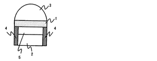
図1〜図6は、本発明に従う白色LEDの実施形態を示す模式的断面図である。図1〜図3に示す実施形態において、蛍光体部材1は、LEDチップ2の上に接触させて設置されている。図1〜図3に示すように蛍光体部材1と、LEDチップ2とを接触させて設置する場合、蛍光体部材1とLEDチップ2の接触部の少なくとも一部に接着剤を塗布し、これにより蛍光体部材1とLEDチップ2とを接着させる。なお、接着剤としては、シリコン、無機接着剤、低融点ガラス等を用いることができる。蛍光体部材1の形状としては、図1に示すような板状、図2に示すような半球レンズ状、図3に示すようなLEDチップ2を覆う蓋形状など様々な形状なものを用いることができる。
(White LED)
1-6 is typical sectional drawing which shows embodiment of white LED according to this invention. In the embodiment shown in FIGS. 1 to 3, the
図4〜図6に示す実施形態2においては、蛍光体部材1を、空気層5を介してLEDチップ2から離して設けている。蛍光体部材1をLEDチップ2から離して設置する場合、蛍光体部材1を支持するための支持部材4などが用いられる。このような支持部材4を用いて、蛍光体部材1が、LEDチップ2から離れるように設置することができる。LEDチップ2から発せられる光を効率的に取り出せるように、図5及び図6に示すように、蛍光体部材1あるいはLEDチップ2の上に、光学部品3(例えばレンズ部品)を設置してもよい。なお、支持部材4への蛍光体部材1の取付け、並びに蛍光体部材1またはLEDチップ2上の光学部品3の取付けは、各部材間の接触部の少なくとも一部に、上記の接着剤を塗布し、接着して取付けることができる。
In the second embodiment shown in FIGS. 4 to 6, the
LEDチップ2としては、GaNにInを添加したInGaNを発光層とする量子井戸構造のLEDチップ等が例示される。なお、電極、n型半導体、p型半導体、サファイア基板などがLEDチップ2に含まれているが図示省略している。光学部品(レンズ部品)3としては、光を効率的に蛍光体部材1に照射するか、あるいは蛍光体部材から発せられる光を集光させるレンズ効果を有する形状であればよく、材質としてはガラス、プラスチック等を用いることができる。支持部材4としては、蛍光体部材1を支持可能な形状を有するものであればよく、ガラス、セラミック、金属等を用いることができる。
Examples of the
本発明の蛍光体材料は、上述のように、白色LEDにおける波長変換部材として用いることができるものであるが、LEDのみならず、レーザダイオード(LD)等のハイパワーの励起光を有する光学部品の蛍光体として用いることができ、一般照明や部分照明、ディスプレイ等の発光装置、自動車等の前照光等に用いることができるものである。 As described above, the phosphor material of the present invention can be used as a wavelength conversion member in a white LED. However, not only the LED but also an optical component having high-power excitation light such as a laser diode (LD). It can be used as general phosphors, partial illuminations, light emitting devices such as displays, headlights of automobiles, and the like.
1…蛍光体部材
2…LEDチップ
3…光学部品
4…支持部材
5…空気層
DESCRIPTION OF
Claims (11)
Priority Applications (1)
| Application Number | Priority Date | Filing Date | Title |
|---|---|---|---|
| JP2007071818A JP2008231218A (en) | 2007-03-20 | 2007-03-20 | Phosphor material and white light-emitting diode |
Applications Claiming Priority (1)
| Application Number | Priority Date | Filing Date | Title |
|---|---|---|---|
| JP2007071818A JP2008231218A (en) | 2007-03-20 | 2007-03-20 | Phosphor material and white light-emitting diode |
Publications (1)
| Publication Number | Publication Date |
|---|---|
| JP2008231218A true JP2008231218A (en) | 2008-10-02 |
Family
ID=39904418
Family Applications (1)
| Application Number | Title | Priority Date | Filing Date |
|---|---|---|---|
| JP2007071818A Pending JP2008231218A (en) | 2007-03-20 | 2007-03-20 | Phosphor material and white light-emitting diode |
Country Status (1)
| Country | Link |
|---|---|
| JP (1) | JP2008231218A (en) |
Cited By (12)
| Publication number | Priority date | Publication date | Assignee | Title |
|---|---|---|---|---|
| JP2010024278A (en) * | 2008-07-16 | 2010-02-04 | Stanley Electric Co Ltd | Phosphor ceramic plate and light-emitting element using it |
| JP2011505450A (en) * | 2007-12-03 | 2011-02-24 | コーニンクレッカ フィリップス エレクトロニクス エヌ ヴィ | Ceramic material for LED with low scattering degree and manufacturing method thereof |
| JP2011108889A (en) * | 2009-11-18 | 2011-06-02 | Asahi Rubber Inc | Light-emitting device |
| JP2012064484A (en) * | 2010-09-17 | 2012-03-29 | Stanley Electric Co Ltd | Light source device |
| JPWO2010103840A1 (en) * | 2009-03-13 | 2012-09-13 | 株式会社小糸製作所 | Light emitting module and lamp unit |
| WO2013136709A1 (en) * | 2012-03-15 | 2013-09-19 | 株式会社小糸製作所 | Light-emitting device and lighting apparatus for vehicle |
| WO2014065028A1 (en) * | 2012-10-23 | 2014-05-01 | 浜松ホトニクス株式会社 | Target for ultraviolet light generation, electron beam-excited ultraviolet light source, and production method for target for ultraviolet light generation |
| JP2016001756A (en) * | 2009-09-17 | 2016-01-07 | コーニンクレッカ フィリップス エヌ ヴェKoninklijke Philips N.V. | Led module with high index lens |
| WO2018037775A1 (en) * | 2016-08-24 | 2018-03-01 | シャープ株式会社 | Light source device and backlight device provided with same, and display device |
| WO2019150747A1 (en) * | 2018-01-30 | 2019-08-08 | パナソニックIpマネジメント株式会社 | Phosphor and method for producing same |
| US11945987B2 (en) | 2018-07-31 | 2024-04-02 | Niterra Co., Ltd. | Light wavelength conversion member and light-emitting device |
| JP7469719B2 (en) | 2021-01-12 | 2024-04-17 | 日亜化学工業株式会社 | Light-emitting device |
Citations (12)
| Publication number | Priority date | Publication date | Assignee | Title |
|---|---|---|---|---|
| JP2001163637A (en) * | 1999-12-08 | 2001-06-19 | Noritake Co Ltd | Method for firing glass film and continuous firing device |
| JP2001203383A (en) * | 1999-09-27 | 2001-07-27 | Lumileds Lighting Us Llc | Light emitting diode device having luminescent substrate performing phosphorescence conversion |
| JP2004146835A (en) * | 2002-10-22 | 2004-05-20 | Osram Opto Semiconductors Gmbh | Light source having led and emitter converter, and method for manufacturing the emitter converter |
| WO2005097938A1 (en) * | 2004-03-31 | 2005-10-20 | Nippon Electric Glass Co., Ltd. | Fluorescent substance and light emitting diode |
| WO2005100281A1 (en) * | 2004-04-07 | 2005-10-27 | Centre National De La Recherche Scientifique (C.N.R.S.) | Preparation of transparent ceramics of yag dope by lanthanides |
| JP2007031196A (en) * | 2005-07-26 | 2007-02-08 | Kyoto Univ | Phosphor, and light emitting diode |
| JP2008019421A (en) * | 2006-06-14 | 2008-01-31 | Nippon Electric Glass Co Ltd | Phosphor composite material and phosphor composite member |
| JP2008021868A (en) * | 2006-07-13 | 2008-01-31 | Nippon Electric Glass Co Ltd | Phosphor composite member |
| JP2008143978A (en) * | 2006-12-07 | 2008-06-26 | Nippon Electric Glass Co Ltd | Luminescent color converting material |
| JP2008530812A (en) * | 2005-02-17 | 2008-08-07 | コーニンクレッカ フィリップス エレクトロニクス エヌ ヴィ | Light source system including a green emissive ceramic luminescence converter |
| JP2008537002A (en) * | 2005-04-19 | 2008-09-11 | コーニンクレッカ フィリップス エレクトロニクス エヌ ヴィ | Lighting system consisting of a ceramic luminescence converter that emits red light |
| JP2008538652A (en) * | 2005-04-20 | 2008-10-30 | コーニンクレッカ フィリップス エレクトロニクス エヌ ヴィ | Lighting system including ceramic luminescence converter |
-
2007
- 2007-03-20 JP JP2007071818A patent/JP2008231218A/en active Pending
Patent Citations (12)
| Publication number | Priority date | Publication date | Assignee | Title |
|---|---|---|---|---|
| JP2001203383A (en) * | 1999-09-27 | 2001-07-27 | Lumileds Lighting Us Llc | Light emitting diode device having luminescent substrate performing phosphorescence conversion |
| JP2001163637A (en) * | 1999-12-08 | 2001-06-19 | Noritake Co Ltd | Method for firing glass film and continuous firing device |
| JP2004146835A (en) * | 2002-10-22 | 2004-05-20 | Osram Opto Semiconductors Gmbh | Light source having led and emitter converter, and method for manufacturing the emitter converter |
| WO2005097938A1 (en) * | 2004-03-31 | 2005-10-20 | Nippon Electric Glass Co., Ltd. | Fluorescent substance and light emitting diode |
| WO2005100281A1 (en) * | 2004-04-07 | 2005-10-27 | Centre National De La Recherche Scientifique (C.N.R.S.) | Preparation of transparent ceramics of yag dope by lanthanides |
| JP2008530812A (en) * | 2005-02-17 | 2008-08-07 | コーニンクレッカ フィリップス エレクトロニクス エヌ ヴィ | Light source system including a green emissive ceramic luminescence converter |
| JP2008537002A (en) * | 2005-04-19 | 2008-09-11 | コーニンクレッカ フィリップス エレクトロニクス エヌ ヴィ | Lighting system consisting of a ceramic luminescence converter that emits red light |
| JP2008538652A (en) * | 2005-04-20 | 2008-10-30 | コーニンクレッカ フィリップス エレクトロニクス エヌ ヴィ | Lighting system including ceramic luminescence converter |
| JP2007031196A (en) * | 2005-07-26 | 2007-02-08 | Kyoto Univ | Phosphor, and light emitting diode |
| JP2008019421A (en) * | 2006-06-14 | 2008-01-31 | Nippon Electric Glass Co Ltd | Phosphor composite material and phosphor composite member |
| JP2008021868A (en) * | 2006-07-13 | 2008-01-31 | Nippon Electric Glass Co Ltd | Phosphor composite member |
| JP2008143978A (en) * | 2006-12-07 | 2008-06-26 | Nippon Electric Glass Co Ltd | Luminescent color converting material |
Non-Patent Citations (4)
| Title |
|---|
| 日本化学会第87春季年会講演予稿集,, JPN6012026434, pages 47 - 2, ISSN: 0002232049 * |
| 第52回応用物理学関係連合講演会講演予稿集,, JPN6012026437, pages 1616 - 30, ISSN: 0002232051 * |
| 第65回応用物理学会学術講演会講演予稿集,, JPN6012026436, pages 1286 - 3, ISSN: 0002232050 * |
| 第66回応用物理学会学術講演会講演予稿集,, JPN6012026439, pages 52 - 9, ISSN: 0002232052 * |
Cited By (20)
| Publication number | Priority date | Publication date | Assignee | Title |
|---|---|---|---|---|
| JP2011505450A (en) * | 2007-12-03 | 2011-02-24 | コーニンクレッカ フィリップス エレクトロニクス エヌ ヴィ | Ceramic material for LED with low scattering degree and manufacturing method thereof |
| JP2010024278A (en) * | 2008-07-16 | 2010-02-04 | Stanley Electric Co Ltd | Phosphor ceramic plate and light-emitting element using it |
| JPWO2010103840A1 (en) * | 2009-03-13 | 2012-09-13 | 株式会社小糸製作所 | Light emitting module and lamp unit |
| JP2016001756A (en) * | 2009-09-17 | 2016-01-07 | コーニンクレッカ フィリップス エヌ ヴェKoninklijke Philips N.V. | Led module with high index lens |
| JP2011108889A (en) * | 2009-11-18 | 2011-06-02 | Asahi Rubber Inc | Light-emitting device |
| JP2012064484A (en) * | 2010-09-17 | 2012-03-29 | Stanley Electric Co Ltd | Light source device |
| US9404631B2 (en) | 2012-03-15 | 2016-08-02 | Koito Manufacturing Co., Ltd. | Light emitting apparatus and automotive lamp |
| JPWO2013136709A1 (en) * | 2012-03-15 | 2015-08-03 | 株式会社小糸製作所 | Light emitting device and vehicle lamp |
| WO2013136709A1 (en) * | 2012-03-15 | 2013-09-19 | 株式会社小糸製作所 | Light-emitting device and lighting apparatus for vehicle |
| WO2014065028A1 (en) * | 2012-10-23 | 2014-05-01 | 浜松ホトニクス株式会社 | Target for ultraviolet light generation, electron beam-excited ultraviolet light source, and production method for target for ultraviolet light generation |
| US9240313B2 (en) | 2012-10-23 | 2016-01-19 | Hamamatsu Photonics K.K. | Target for ultraviolet light generation, electron beam-excited ultraviolet light source, and production method for target for ultraviolet light generation |
| WO2018037775A1 (en) * | 2016-08-24 | 2018-03-01 | シャープ株式会社 | Light source device and backlight device provided with same, and display device |
| CN111051932A (en) * | 2018-01-30 | 2020-04-21 | 松下知识产权经营株式会社 | Phosphor and method for producing same |
| WO2019150747A1 (en) * | 2018-01-30 | 2019-08-08 | パナソニックIpマネジメント株式会社 | Phosphor and method for producing same |
| JPWO2019150747A1 (en) * | 2018-01-30 | 2021-02-04 | パナソニックIpマネジメント株式会社 | Fluorescent material and its manufacturing method |
| EP3748406A4 (en) * | 2018-01-30 | 2021-03-24 | Panasonic Intellectual Property Management Co., Ltd. | Phosphor and method for producing same |
| US10995935B2 (en) | 2018-01-30 | 2021-05-04 | Panasonic Intellectual Property Management Co., Ltd. | Phosphor and method for producing same |
| CN111051932B (en) * | 2018-01-30 | 2022-03-22 | 松下知识产权经营株式会社 | Phosphor and method for producing same |
| US11945987B2 (en) | 2018-07-31 | 2024-04-02 | Niterra Co., Ltd. | Light wavelength conversion member and light-emitting device |
| JP7469719B2 (en) | 2021-01-12 | 2024-04-17 | 日亜化学工業株式会社 | Light-emitting device |
Similar Documents
| Publication | Publication Date | Title |
|---|---|---|
| JP2008231218A (en) | Phosphor material and white light-emitting diode | |
| KR102271648B1 (en) | Wavelength conversion member and light emitting device using same | |
| JP6273799B2 (en) | Glass used for wavelength conversion material, wavelength conversion material, wavelength conversion member, and light emitting device | |
| JP6941821B2 (en) | Wavelength converter, its manufacturing method, and light emitting device using the wavelength converter | |
| JP2008088257A (en) | Phosphor material, phosphor material sheet, method for producing phosphor material, and light-emitting device by using the phosphor material | |
| CN111213075B (en) | Wavelength conversion member and light emitting device | |
| JP2006310817A (en) | Incandescent emitting device and luminaire | |
| JP6718991B2 (en) | Lutetium nitride fluorescent powder and light emitting device having the fluorescent powder | |
| TWI668295B (en) | Optical wavelength conversion member and light emitting device | |
| JP6365828B2 (en) | Glass used for wavelength conversion material, wavelength conversion material, wavelength conversion member, and light emitting device | |
| JP2007059898A (en) | Semiconductor light-emitting device | |
| WO2009099234A1 (en) | Light emitting device and manufacturing method of same | |
| JP2014221890A (en) | Phosphor, phosphor-containing composition, light-emitting device, image display device, and lighting device | |
| JP6591951B2 (en) | Light wavelength conversion member and light emitting device | |
| JP2009215495A (en) | Fluorescent material | |
| JP6989307B2 (en) | Ceramic complexes, as well as fluorescent and light-emitting devices for projectors containing them | |
| JP6273464B2 (en) | Red phosphor material and light emitting device | |
| JP2006332202A (en) | Light emitting device, manufacturing method thereof, and lighting apparatus using it, backlight for image display apparatus, and image display apparatus | |
| JP2014003070A (en) | Light-emitting device and lighting apparatus | |
| JP7147138B2 (en) | Light-emitting device, lighting device, image display device, and vehicle indicator light | |
| JP6499237B2 (en) | Light wavelength conversion member and light emitting device | |
| JP2011225803A (en) | Fluorescent material, method for manufacturing the same, and light-emitting device having the same | |
| TWI619906B (en) | Phosphor plate using light diffusing agent | |
| JP6486315B2 (en) | Light wavelength conversion member and light emitting device | |
| JP5807780B2 (en) | Wavelength converting member and light emitting device using the same |
Legal Events
| Date | Code | Title | Description |
|---|---|---|---|
| A621 | Written request for application examination |
Free format text: JAPANESE INTERMEDIATE CODE: A621 Effective date: 20091204 |
|
| A977 | Report on retrieval |
Free format text: JAPANESE INTERMEDIATE CODE: A971007 Effective date: 20120511 |
|
| A131 | Notification of reasons for refusal |
Free format text: JAPANESE INTERMEDIATE CODE: A131 Effective date: 20120529 |
|
| A02 | Decision of refusal |
Free format text: JAPANESE INTERMEDIATE CODE: A02 Effective date: 20121002 |