JP2008227251A - Insulated gate transistor - Google Patents
Insulated gate transistor Download PDFInfo
- Publication number
- JP2008227251A JP2008227251A JP2007064995A JP2007064995A JP2008227251A JP 2008227251 A JP2008227251 A JP 2008227251A JP 2007064995 A JP2007064995 A JP 2007064995A JP 2007064995 A JP2007064995 A JP 2007064995A JP 2008227251 A JP2008227251 A JP 2008227251A
- Authority
- JP
- Japan
- Prior art keywords
- trench
- layer
- source
- base layer
- charge storage
- Prior art date
- Legal status (The legal status is an assumption and is not a legal conclusion. Google has not performed a legal analysis and makes no representation as to the accuracy of the status listed.)
- Pending
Links
- 239000004065 semiconductor Substances 0.000 claims abstract description 12
- 239000000758 substrate Substances 0.000 claims abstract description 12
- 230000000149 penetrating effect Effects 0.000 claims description 4
- 238000009413 insulation Methods 0.000 claims 1
- 230000015556 catabolic process Effects 0.000 abstract description 5
- 230000006866 deterioration Effects 0.000 abstract 1
- 230000006378 damage Effects 0.000 description 4
- 239000006185 dispersion Substances 0.000 description 3
- 230000015572 biosynthetic process Effects 0.000 description 2
- 230000007423 decrease Effects 0.000 description 2
- 238000000034 method Methods 0.000 description 2
- 238000013459 approach Methods 0.000 description 1
- 230000003071 parasitic effect Effects 0.000 description 1
Images


Classifications
-
- H—ELECTRICITY
- H01—ELECTRIC ELEMENTS
- H01L—SEMICONDUCTOR DEVICES NOT COVERED BY CLASS H10
- H01L29/00—Semiconductor devices adapted for rectifying, amplifying, oscillating or switching, or capacitors or resistors with at least one potential-jump barrier or surface barrier, e.g. PN junction depletion layer or carrier concentration layer; Details of semiconductor bodies or of electrodes thereof ; Multistep manufacturing processes therefor
- H01L29/66—Types of semiconductor device ; Multistep manufacturing processes therefor
- H01L29/68—Types of semiconductor device ; Multistep manufacturing processes therefor controllable by only the electric current supplied, or only the electric potential applied, to an electrode which does not carry the current to be rectified, amplified or switched
- H01L29/70—Bipolar devices
- H01L29/72—Transistor-type devices, i.e. able to continuously respond to applied control signals
- H01L29/739—Transistor-type devices, i.e. able to continuously respond to applied control signals controlled by field-effect, e.g. bipolar static induction transistors [BSIT]
- H01L29/7393—Insulated gate bipolar mode transistors, i.e. IGBT; IGT; COMFET
- H01L29/7395—Vertical transistors, e.g. vertical IGBT
- H01L29/7396—Vertical transistors, e.g. vertical IGBT with a non planar surface, e.g. with a non planar gate or with a trench or recess or pillar in the surface of the emitter, base or collector region for improving current density or short circuiting the emitter and base regions
- H01L29/7397—Vertical transistors, e.g. vertical IGBT with a non planar surface, e.g. with a non planar gate or with a trench or recess or pillar in the surface of the emitter, base or collector region for improving current density or short circuiting the emitter and base regions and a gate structure lying on a slanted or vertical surface or formed in a groove, e.g. trench gate IGBT
-
- H—ELECTRICITY
- H01—ELECTRIC ELEMENTS
- H01L—SEMICONDUCTOR DEVICES NOT COVERED BY CLASS H10
- H01L29/00—Semiconductor devices adapted for rectifying, amplifying, oscillating or switching, or capacitors or resistors with at least one potential-jump barrier or surface barrier, e.g. PN junction depletion layer or carrier concentration layer; Details of semiconductor bodies or of electrodes thereof ; Multistep manufacturing processes therefor
- H01L29/02—Semiconductor bodies ; Multistep manufacturing processes therefor
- H01L29/06—Semiconductor bodies ; Multistep manufacturing processes therefor characterised by their shape; characterised by the shapes, relative sizes, or dispositions of the semiconductor regions ; characterised by the concentration or distribution of impurities within semiconductor regions
- H01L29/0684—Semiconductor bodies ; Multistep manufacturing processes therefor characterised by their shape; characterised by the shapes, relative sizes, or dispositions of the semiconductor regions ; characterised by the concentration or distribution of impurities within semiconductor regions characterised by the shape, relative sizes or dispositions of the semiconductor regions or junctions between the regions
- H01L29/0692—Surface layout
- H01L29/0696—Surface layout of cellular field-effect devices, e.g. multicellular DMOS transistors or IGBTs
-
- H—ELECTRICITY
- H01—ELECTRIC ELEMENTS
- H01L—SEMICONDUCTOR DEVICES NOT COVERED BY CLASS H10
- H01L29/00—Semiconductor devices adapted for rectifying, amplifying, oscillating or switching, or capacitors or resistors with at least one potential-jump barrier or surface barrier, e.g. PN junction depletion layer or carrier concentration layer; Details of semiconductor bodies or of electrodes thereof ; Multistep manufacturing processes therefor
- H01L29/02—Semiconductor bodies ; Multistep manufacturing processes therefor
- H01L29/06—Semiconductor bodies ; Multistep manufacturing processes therefor characterised by their shape; characterised by the shapes, relative sizes, or dispositions of the semiconductor regions ; characterised by the concentration or distribution of impurities within semiconductor regions
- H01L29/08—Semiconductor bodies ; Multistep manufacturing processes therefor characterised by their shape; characterised by the shapes, relative sizes, or dispositions of the semiconductor regions ; characterised by the concentration or distribution of impurities within semiconductor regions with semiconductor regions connected to an electrode carrying current to be rectified, amplified or switched and such electrode being part of a semiconductor device which comprises three or more electrodes
- H01L29/083—Anode or cathode regions of thyristors or gated bipolar-mode devices
- H01L29/0834—Anode regions of thyristors or gated bipolar-mode devices, e.g. supplementary regions surrounding anode regions
-
- H—ELECTRICITY
- H01—ELECTRIC ELEMENTS
- H01L—SEMICONDUCTOR DEVICES NOT COVERED BY CLASS H10
- H01L29/00—Semiconductor devices adapted for rectifying, amplifying, oscillating or switching, or capacitors or resistors with at least one potential-jump barrier or surface barrier, e.g. PN junction depletion layer or carrier concentration layer; Details of semiconductor bodies or of electrodes thereof ; Multistep manufacturing processes therefor
- H01L29/66—Types of semiconductor device ; Multistep manufacturing processes therefor
- H01L29/66007—Multistep manufacturing processes
- H01L29/66075—Multistep manufacturing processes of devices having semiconductor bodies comprising group 14 or group 13/15 materials
- H01L29/66227—Multistep manufacturing processes of devices having semiconductor bodies comprising group 14 or group 13/15 materials the devices being controllable only by the electric current supplied or the electric potential applied, to an electrode which does not carry the current to be rectified, amplified or switched, e.g. three-terminal devices
- H01L29/66234—Bipolar junction transistors [BJT]
- H01L29/66325—Bipolar junction transistors [BJT] controlled by field-effect, e.g. insulated gate bipolar transistors [IGBT]
Abstract
Description
本発明は、インバータ装置等を構成する絶縁ゲート型トランジスタに関し、特に短絡モード時の電流ばらつきや破壊耐量の低下を抑制することができる絶縁ゲート型トランジスタに関するものである。 The present invention relates to an insulated gate transistor that constitutes an inverter device and the like, and more particularly to an insulated gate transistor that can suppress current variation and a reduction in breakdown resistance in a short-circuit mode.
トレンチゲート構造の絶縁ゲート型トランジスタ(IGBT)において、短絡モード時の電流低減及び破壊を防ぐために、ダミートレンチを設けてチャネルが形成されない領域を設けている品種がある(例えば、特許文献1参照)。 In an insulated gate transistor (IGBT) having a trench gate structure, there is a product type in which a dummy trench is provided to provide a region where a channel is not formed in order to prevent current reduction and destruction in a short-circuit mode (see, for example, Patent Document 1). .
図4は、従来の絶縁ゲート型トランジスタを示す上面図である。トレンチ14の両側にダミートレンチ17が形成されている。トレンチ14の側壁に接するようにp型のベース層13の表面にn型のソース層21が選択的に形成されている。ベース層13の表面においてトレンチ14とダミートレンチ17との間にp+型のコンタクト層22が形成されている。
FIG. 4 is a top view showing a conventional insulated gate transistor. Dummy
従来の絶縁ゲート型トランジスタでは、コンタクト層22とトレンチ14との間の領域にソース層21が存在していた。そして、この領域がソースバラスト抵抗27となっていた。しかし、ソース形成工程とトレンチ形成工程のパターン加工精度により、ソースバラスト抵抗27の抵抗値にばらつきが発生していた。これにより、短絡モード時の電流ばらつきや破壊耐量の低下を引き起こすという問題があった。
In the conventional insulated gate transistor, the
本発明は、上述のような課題を解決するためになされたもので、その目的は、短絡モード時の電流ばらつきや破壊耐量の低下を抑制することができる絶縁ゲート型トランジスタを得るものである。 The present invention has been made to solve the above-described problems, and an object of the present invention is to obtain an insulated gate transistor capable of suppressing current variations and a reduction in breakdown resistance in the short-circuit mode.
本発明に係る絶縁ゲート型トランジスタは、第1及び第2主面を有する第1導電型の半導体基板と、半導体基板の第1主面に形成された第1導電型の電荷蓄積層と、電荷蓄積層上に形成された第2導電型のベース層と、ベース層及び電荷蓄積層を貫通するトレンチの内部に絶縁膜を介して埋め込まれたトレンチゲート電極と、トレンチの両側に配置されてベース層及び電荷蓄積層を貫通するダミートレンチの内部に絶縁膜を介して埋め込まれ、トレンチゲート電極とは電気的に非接続であるダミートレンチゲート電極と、トレンチの側壁に接するようにベース層の表面に選択的に形成され、トレンチの長手方向に離散的に並んだ第1導電型のソース層と、ベース層の表面において、トレンチの長手方向に並んだソース層同士の間に形成された第2導電型のコンタクト層と、半導体基板の第2主面に形成された第2導電型のコレクタ層と、ソース層及びコンタクト層に接続されたエミッタ電極と、コレクタ層に接続されたコレクタ電極とを有する。本発明のその他の特徴は以下に明らかにする。 An insulated gate transistor according to the present invention includes a first conductive type semiconductor substrate having first and second main surfaces, a first conductive type charge storage layer formed on the first main surface of the semiconductor substrate, A base layer of a second conductivity type formed on the storage layer; a trench gate electrode embedded through an insulating film in a trench penetrating the base layer and the charge storage layer; and a base disposed on both sides of the trench A dummy trench gate electrode embedded in an inside of a dummy trench penetrating the layer and the charge storage layer via an insulating film, and being electrically disconnected from the trench gate electrode, and a surface of the base layer so as to be in contact with the side wall of the trench Formed between the source layers of the first conductivity type discretely arranged in the longitudinal direction of the trench and the source layers arranged in the longitudinal direction of the trench on the surface of the base layer. A second conductivity type contact layer; a second conductivity type collector layer formed on the second main surface of the semiconductor substrate; an emitter electrode connected to the source layer and the contact layer; a collector electrode connected to the collector layer; Have Other features of the present invention will become apparent below.
本発明により、短絡モード時の電流ばらつきや破壊耐量の低下を抑制することができる。 According to the present invention, it is possible to suppress current variation and breakdown resistance reduction in the short circuit mode.
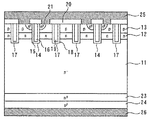
実施の形態1.
図1は、本発明の実施の形態1に係る絶縁ゲート型トランジスタを示す上面図であり、図2は図1のA−A´における断面図である。
Embodiment 1 FIG.
FIG. 1 is a top view showing an insulated gate transistor according to Embodiment 1 of the present invention, and FIG. 2 is a cross-sectional view taken along line AA ′ of FIG.
n−型の半導体基板11の上面(第1主面)に、n型の電荷蓄積層12が形成されている。電荷蓄積層12上にp型のベース層13が形成されている。
An n - type
ベース層13及び電荷蓄積層12を貫通するようにストライプ状のトレンチ14が複数個、平行に形成されている。このトレンチ14の内部に絶縁膜15を介してトレンチゲート電極16が埋め込まれている。トレンチ14の両側に、ベース層13及び電荷蓄積層12を貫通するようにストライプ状のダミートレンチ17が平行に形成されている。このダミートレンチ17の内部に絶縁膜18を介してダミートレンチゲート電極19が埋め込まれている。ダミートレンチゲート電極19は、トレンチゲート電極16とは電気的に非接続である。トレンチゲート電極16及びダミートレンチゲート電極19上には絶縁膜20が形成されている。
A plurality of stripe-
トレンチ14の側壁に接するようにベース層13の表面にn+型のソース層21が選択的に形成されている。ソース層21はトレンチ14の長手方向に離散的に並んでいる。ベース層13の表面において、トレンチ14の長手方向に並んだソース層21同士の間にp+型のコンタクト層22が形成されている。
An n + -
半導体基板11の下面(第2主面)に、n+型のバッファ層23が形成されている。バッファ層23の下にp+型のコレクタ層24が形成されている。エミッタ電極25がソース層21及びコンタクト層22に接続され、コレクタ電極26がコレクタ層24に接続されている。
An n + -type buffer layer 23 is formed on the lower surface (second main surface) of the
上記のように、本実施の形態に係る絶縁ゲート型トランジスタは、p型のベース層13の下にキャリア蓄積のためにn型の電荷蓄積層12を形成したキャリア蓄積型トレンチIGBTである。従来のトレンチIGBTでは正孔密度がエミッタ側に近付くにつれて減少していたのに対し、このキャリア蓄積型トレンチIGBTでは、エミッタ側でも高い正孔濃度が保てるためオン電圧(飽和電圧)も減少する。その結果、飽和電圧とターン・オフ・エネルギーのトレードオフの関係も改善することができる。
As described above, the insulated gate transistor according to the present embodiment is a carrier storage trench IGBT in which the n-type
また、n+型のソース層21とp+型のコンタクト層22はトレンチ14の長手方向に交互に形成されているため、n+型のソース層21とp型のベース層13とはエミッタ電極25によってチャネル幅方向で短絡する。これにより、n型のソース層21、p型のベース層13、n型の半導体基板11及びp型のコレクタ層24で構成されたnpnpサイリスタのラッチアップを防止することができる。
Further, since the n + -
また、本実施の形態では、ソース層21をトレンチ14の長手方向に離散的に並べている。従って、コンタクト層22とトレンチ14との間の領域にソース層21が存在しない。即ち、パターン加工精度によって抵抗値がばらつくソースバラスト抵抗が存在しない。これにより、短絡モード時の電流ばらつきや破壊耐量の低下を抑制することができる。
In the present embodiment, the
ここで、通電能力と短絡電流のトレードオフにより最適なソース層21のパターンを選定する必要がある。そこで、トレンチ14の長手方向に並んだソース層21同士の間隔Wgateに対するトレンチ14の長手方向におけるソース層21の幅(チャネル幅)Wchの比率(Wch/Wgate)が1/2〜1/10となるように、ソース層21のパターンを形成するのが好ましい。これにより、短絡電流ばらつき及び破壊耐量低下を抑制することができる。
Here, it is necessary to select an optimum pattern of the
また、ダミートレンチゲート電極19をエミッタ電極25と同電位(GND)とするのが好ましい。これにより、ゲート容量を低減することができる。
The dummy trench gate electrode 19 is preferably set to the same potential (GND) as the
また、ソース層21の幅Wchを1.0μm以上とするのが好ましい。これにより、ソース層21形成時のパターン加工精度が±0.2μmの場合、ソース層21の幅Wchのばらつきによる短絡電流ばらつきを20%以内に抑制することができる。従って、短絡電流ばらつきを抑制しつつ、最適なソース層21のパターンを選定することができる。
The width Wch of the
実施の形態2.
図3は、本発明の実施の形態2に係る絶縁ゲート型トランジスタを示す上面図である。図示のように、ソース層21は部分的な切り欠きを有する。その他の構成は実施の形態1と同様である。これにより、ソース層21下のベース層13の抵抗を低減することができる。従って、絶縁ゲート型トランジスタの寄生トランジスタによるラッチアップを抑制し、破壊耐量低下を抑制することができる。
FIG. 3 is a top view showing an insulated gate transistor according to the second embodiment of the present invention. As shown, the
11 半導体基板
12 電荷蓄積層
13 ベース層
14 トレンチ
15 絶縁膜
16 トレンチゲート電極
17 ダミートレンチ
18,20 絶縁膜
19 ダミートレンチゲート電極
21 ソース層
22 コンタクト層
24 コレクタ層
25 エミッタ電極
26 コレクタ電極
11
Claims (5)
前記半導体基板の第1主面に形成された第1導電型の電荷蓄積層と、
前記電荷蓄積層上に形成された第2導電型のベース層と、
前記ベース層及び前記電荷蓄積層を貫通するストライプ状のトレンチの内部に絶縁膜を介して埋め込まれたトレンチゲート電極と、
前記トレンチの両側に配置されて前記ベース層及び前記電荷蓄積層を貫通するストライプ状のダミートレンチの内部に絶縁膜を介して埋め込まれ、前記トレンチゲート電極とは電気的に非接続であるダミートレンチゲート電極と、
前記トレンチの側壁に接するように前記ベース層の表面に選択的に形成され、前記トレンチの長手方向に離散的に並んだ第1導電型のソース層と、
前記ベース層の表面において、前記トレンチの長手方向に並んだ前記ソース層同士の間に形成された第2導電型のコンタクト層と、
前記半導体基板の第2主面に形成された第2導電型のコレクタ層と、
前記ソース層及び前記コンタクト層に接続されたエミッタ電極と、
前記コレクタ層に接続されたコレクタ電極とを有する絶縁ゲート型トランジスタ。 A first conductivity type semiconductor substrate having first and second main surfaces;
A charge storage layer of a first conductivity type formed on the first main surface of the semiconductor substrate;
A second conductivity type base layer formed on the charge storage layer;
A trench gate electrode embedded through an insulating film inside a stripe-shaped trench penetrating the base layer and the charge storage layer;
A dummy trench which is disposed on both sides of the trench and is embedded in an inside of a striped dummy trench penetrating the base layer and the charge storage layer via an insulating film, and is electrically disconnected from the trench gate electrode A gate electrode;
A source layer of a first conductivity type selectively formed on the surface of the base layer so as to be in contact with a sidewall of the trench and discretely arranged in a longitudinal direction of the trench;
A contact layer of a second conductivity type formed between the source layers arranged in the longitudinal direction of the trench on the surface of the base layer;
A collector layer of a second conductivity type formed on the second main surface of the semiconductor substrate;
An emitter electrode connected to the source layer and the contact layer;
An insulated gate transistor having a collector electrode connected to the collector layer.
The insulated gate transistor according to claim 1, wherein the source layer has a partial notch.
Priority Applications (4)
| Application Number | Priority Date | Filing Date | Title |
|---|---|---|---|
| JP2007064995A JP2008227251A (en) | 2007-03-14 | 2007-03-14 | Insulated gate transistor |
| US11/843,301 US7675113B2 (en) | 2007-03-14 | 2007-08-22 | Insulated gate transistor |
| DE102007057222A DE102007057222B4 (en) | 2007-03-14 | 2007-11-28 | Isolated gate transistor |
| KR1020070123240A KR100935165B1 (en) | 2007-03-14 | 2007-11-30 | Insulated Gate Transistor |
Applications Claiming Priority (1)
| Application Number | Priority Date | Filing Date | Title |
|---|---|---|---|
| JP2007064995A JP2008227251A (en) | 2007-03-14 | 2007-03-14 | Insulated gate transistor |
Publications (1)
| Publication Number | Publication Date |
|---|---|
| JP2008227251A true JP2008227251A (en) | 2008-09-25 |
Family
ID=39713294
Family Applications (1)
| Application Number | Title | Priority Date | Filing Date |
|---|---|---|---|
| JP2007064995A Pending JP2008227251A (en) | 2007-03-14 | 2007-03-14 | Insulated gate transistor |
Country Status (4)
| Country | Link |
|---|---|
| US (1) | US7675113B2 (en) |
| JP (1) | JP2008227251A (en) |
| KR (1) | KR100935165B1 (en) |
| DE (1) | DE102007057222B4 (en) |
Cited By (8)
| Publication number | Priority date | Publication date | Assignee | Title |
|---|---|---|---|---|
| JP2012114321A (en) * | 2010-11-26 | 2012-06-14 | Mitsubishi Electric Corp | Semiconductor device |
| US8604544B2 (en) | 2010-03-24 | 2013-12-10 | Kabushiki Kaisha Toshiba | Semiconductor device |
| JP2016082167A (en) * | 2014-10-21 | 2016-05-16 | 株式会社デンソー | Semiconductor device |
| JP2017147300A (en) * | 2016-02-16 | 2017-08-24 | 富士電機株式会社 | Semiconductor device |
| CN109524396A (en) * | 2017-09-20 | 2019-03-26 | 株式会社东芝 | Semiconductor device |
| US11282949B2 (en) | 2020-03-19 | 2022-03-22 | Kabushiki Kaisha Toshiba | Semiconductor device and semiconductor circuit |
| JP2022059083A (en) * | 2017-05-16 | 2022-04-12 | 富士電機株式会社 | Semiconductor device |
| JP7320910B2 (en) | 2020-09-18 | 2023-08-04 | 株式会社東芝 | Semiconductor device and its control method |
Families Citing this family (32)
| Publication number | Priority date | Publication date | Assignee | Title |
|---|---|---|---|---|
| US7785946B2 (en) | 2007-09-25 | 2010-08-31 | Infineon Technologies Ag | Integrated circuits and methods of design and manufacture thereof |
| JP4256901B1 (en) * | 2007-12-21 | 2009-04-22 | 株式会社豊田中央研究所 | Semiconductor device |
| JP4688901B2 (en) * | 2008-05-13 | 2011-05-25 | 三菱電機株式会社 | Semiconductor device |
| WO2014125583A1 (en) | 2013-02-13 | 2014-08-21 | トヨタ自動車株式会社 | Semiconductor device |
| US10249721B2 (en) | 2013-04-04 | 2019-04-02 | Infineon Technologies Austria Ag | Semiconductor device including a gate trench and a source trench |
| US9666663B2 (en) | 2013-08-09 | 2017-05-30 | Infineon Technologies Ag | Semiconductor device with cell trench structures and contacts and method of manufacturing a semiconductor device |
| US9076838B2 (en) | 2013-09-13 | 2015-07-07 | Infineon Technologies Ag | Insulated gate bipolar transistor with mesa sections between cell trench structures and method of manufacturing |
| US9385228B2 (en) | 2013-11-27 | 2016-07-05 | Infineon Technologies Ag | Semiconductor device with cell trench structures and contacts and method of manufacturing a semiconductor device |
| US9105679B2 (en) * | 2013-11-27 | 2015-08-11 | Infineon Technologies Ag | Semiconductor device and insulated gate bipolar transistor with barrier regions |
| US9553179B2 (en) | 2014-01-31 | 2017-01-24 | Infineon Technologies Ag | Semiconductor device and insulated gate bipolar transistor with barrier structure |
| US10608104B2 (en) | 2014-03-28 | 2020-03-31 | Infineon Technologies Ag | Trench transistor device |
| CN103956379B (en) * | 2014-05-09 | 2017-01-04 | 常州中明半导体技术有限公司 | Have and optimize the CSTBT device embedding primitive cell structure |
| CN104157684B (en) * | 2014-08-25 | 2017-02-08 | 株洲南车时代电气股份有限公司 | Trench gate IGBT chip |
| KR101955055B1 (en) | 2014-11-28 | 2019-03-07 | 매그나칩 반도체 유한회사 | Power semiconductor device and method of fabricating the same |
| CN107534053A (en) * | 2015-01-14 | 2018-01-02 | 三菱电机株式会社 | Semiconductor device and its manufacture method |
| US9583605B2 (en) * | 2015-02-05 | 2017-02-28 | Changzhou ZhongMin Semi-Tech Co. Ltd | Method of forming a trench in a semiconductor device |
| US10529839B2 (en) * | 2015-05-15 | 2020-01-07 | Fuji Electric Co., Ltd. | Semiconductor device |
| CN105304697B (en) * | 2015-11-10 | 2019-02-15 | 株洲南车时代电气股份有限公司 | A kind of igbt chip and preparation method thereof |
| CN105390537B (en) * | 2015-11-10 | 2018-12-21 | 株洲南车时代电气股份有限公司 | A kind of trench gate IGBT and preparation method thereof |
| CN105226090B (en) * | 2015-11-10 | 2018-07-13 | 株洲中车时代电气股份有限公司 | A kind of igbt and preparation method thereof |
| CN108292676B (en) * | 2015-12-07 | 2020-11-13 | 三菱电机株式会社 | Silicon carbide semiconductor device |
| DE112017000063T5 (en) * | 2016-02-15 | 2018-03-22 | Fuji Electric Co., Ltd. | Semiconductor device |
| KR101836256B1 (en) | 2016-06-24 | 2018-03-08 | 현대자동차 주식회사 | Semiconductor device and method manufacturing the same |
| CN109075192B (en) * | 2016-10-17 | 2021-10-26 | 富士电机株式会社 | Semiconductor device with a plurality of semiconductor chips |
| CN109155332B (en) * | 2016-11-17 | 2021-07-23 | 富士电机株式会社 | Semiconductor device with a plurality of semiconductor chips |
| CN106783951B (en) * | 2016-12-23 | 2020-03-24 | 株洲中车时代电气股份有限公司 | Semiconductor device and forming method thereof |
| CN109478570B (en) * | 2017-02-15 | 2021-08-31 | 富士电机株式会社 | Semiconductor device with a plurality of semiconductor chips |
| US10388726B2 (en) * | 2017-10-24 | 2019-08-20 | Semiconductor Components Industries, Llc | Accumulation enhanced insulated gate bipolar transistor (AEGT) and methods of use thereof |
| CN109192771B (en) * | 2018-08-29 | 2020-06-30 | 电子科技大学 | Charge storage type insulated gate bipolar transistor and preparation method thereof |
| CN110504305B (en) * | 2019-08-06 | 2021-02-05 | 电子科技大学 | SOI-LIGBT device with self-biased pmos clamp carrier storage layer |
| CN113054009B (en) * | 2019-12-27 | 2024-02-23 | 株洲中车时代半导体有限公司 | Groove IGBT chip |
| JP7459703B2 (en) * | 2020-07-15 | 2024-04-02 | 富士電機株式会社 | Semiconductor Device |
Citations (8)
| Publication number | Priority date | Publication date | Assignee | Title |
|---|---|---|---|---|
| JPH11345969A (en) * | 1998-06-01 | 1999-12-14 | Toshiba Corp | Power semiconductor device |
| JP2000106434A (en) * | 1998-09-29 | 2000-04-11 | Toshiba Corp | High-breakdown voltage semiconductor device |
| JP2002100770A (en) * | 2000-09-22 | 2002-04-05 | Toshiba Corp | Insulating gate type semiconductor device |
| WO2002058160A1 (en) * | 2001-01-19 | 2002-07-25 | Mitsubishi Denki Kabushiki Kaisha | Semiconductor device |
| JP2004022941A (en) * | 2002-06-19 | 2004-01-22 | Toshiba Corp | Semiconductor device |
| JP2004153112A (en) * | 2002-10-31 | 2004-05-27 | Toshiba Corp | Power semiconductor device |
| JP2006203550A (en) * | 2005-01-20 | 2006-08-03 | Hitachi Kokusai Electric Inc | Radio base station apparatus |
| JP2006253636A (en) * | 2005-02-10 | 2006-09-21 | Sanken Electric Co Ltd | Semiconductor element |
Family Cites Families (8)
| Publication number | Priority date | Publication date | Assignee | Title |
|---|---|---|---|---|
| JP3647676B2 (en) * | 1999-06-30 | 2005-05-18 | 株式会社東芝 | Semiconductor device |
| JP3344381B2 (en) * | 1999-08-23 | 2002-11-11 | 日本電気株式会社 | Semiconductor device and manufacturing method thereof |
| JP2002016252A (en) | 2000-06-27 | 2002-01-18 | Toshiba Corp | Insulation gate type semiconductor element |
| JP4823435B2 (en) | 2001-05-29 | 2011-11-24 | 三菱電機株式会社 | Semiconductor device and manufacturing method thereof |
| JP3971327B2 (en) * | 2003-03-11 | 2007-09-05 | 株式会社東芝 | Insulated gate semiconductor device |
| US7423316B2 (en) | 2004-05-12 | 2008-09-09 | Kabushiki Kaisha Toyota Chuo Kenkyusho | Semiconductor devices |
| JP4575713B2 (en) * | 2004-05-31 | 2010-11-04 | 三菱電機株式会社 | Insulated gate semiconductor device |
| JP5040240B2 (en) * | 2006-09-29 | 2012-10-03 | 三菱電機株式会社 | Insulated gate semiconductor device |
-
2007
- 2007-03-14 JP JP2007064995A patent/JP2008227251A/en active Pending
- 2007-08-22 US US11/843,301 patent/US7675113B2/en not_active Expired - Fee Related
- 2007-11-28 DE DE102007057222A patent/DE102007057222B4/en not_active Expired - Fee Related
- 2007-11-30 KR KR1020070123240A patent/KR100935165B1/en not_active IP Right Cessation
Patent Citations (8)
| Publication number | Priority date | Publication date | Assignee | Title |
|---|---|---|---|---|
| JPH11345969A (en) * | 1998-06-01 | 1999-12-14 | Toshiba Corp | Power semiconductor device |
| JP2000106434A (en) * | 1998-09-29 | 2000-04-11 | Toshiba Corp | High-breakdown voltage semiconductor device |
| JP2002100770A (en) * | 2000-09-22 | 2002-04-05 | Toshiba Corp | Insulating gate type semiconductor device |
| WO2002058160A1 (en) * | 2001-01-19 | 2002-07-25 | Mitsubishi Denki Kabushiki Kaisha | Semiconductor device |
| JP2004022941A (en) * | 2002-06-19 | 2004-01-22 | Toshiba Corp | Semiconductor device |
| JP2004153112A (en) * | 2002-10-31 | 2004-05-27 | Toshiba Corp | Power semiconductor device |
| JP2006203550A (en) * | 2005-01-20 | 2006-08-03 | Hitachi Kokusai Electric Inc | Radio base station apparatus |
| JP2006253636A (en) * | 2005-02-10 | 2006-09-21 | Sanken Electric Co Ltd | Semiconductor element |
Cited By (10)
| Publication number | Priority date | Publication date | Assignee | Title |
|---|---|---|---|---|
| US8604544B2 (en) | 2010-03-24 | 2013-12-10 | Kabushiki Kaisha Toshiba | Semiconductor device |
| US9299695B2 (en) | 2010-03-24 | 2016-03-29 | Kabushiki Kaisha Toshiba | Semiconductor device |
| JP2012114321A (en) * | 2010-11-26 | 2012-06-14 | Mitsubishi Electric Corp | Semiconductor device |
| JP2016082167A (en) * | 2014-10-21 | 2016-05-16 | 株式会社デンソー | Semiconductor device |
| JP2017147300A (en) * | 2016-02-16 | 2017-08-24 | 富士電機株式会社 | Semiconductor device |
| JP2022059083A (en) * | 2017-05-16 | 2022-04-12 | 富士電機株式会社 | Semiconductor device |
| JP7435645B2 (en) | 2017-05-16 | 2024-02-21 | 富士電機株式会社 | semiconductor equipment |
| CN109524396A (en) * | 2017-09-20 | 2019-03-26 | 株式会社东芝 | Semiconductor device |
| US11282949B2 (en) | 2020-03-19 | 2022-03-22 | Kabushiki Kaisha Toshiba | Semiconductor device and semiconductor circuit |
| JP7320910B2 (en) | 2020-09-18 | 2023-08-04 | 株式会社東芝 | Semiconductor device and its control method |
Also Published As
| Publication number | Publication date |
|---|---|
| US7675113B2 (en) | 2010-03-09 |
| DE102007057222A1 (en) | 2008-09-25 |
| DE102007057222B4 (en) | 2012-05-31 |
| KR100935165B1 (en) | 2010-01-06 |
| US20080224207A1 (en) | 2008-09-18 |
| KR20080086963A (en) | 2008-09-29 |
Similar Documents
| Publication | Publication Date | Title |
|---|---|---|
| JP2008227251A (en) | Insulated gate transistor | |
| US10192978B2 (en) | Semiconductor apparatus | |
| JP5340695B2 (en) | Trench gate type insulated gate bipolar transistor | |
| US20150091055A1 (en) | Semiconductor device | |
| WO2017199679A1 (en) | Semiconductor device | |
| JP6356803B2 (en) | Insulated gate bipolar transistor | |
| JP2012064641A (en) | Semiconductor device | |
| JP5821320B2 (en) | diode | |
| JP6471508B2 (en) | Semiconductor device | |
| JP2007258363A (en) | Semiconductor device | |
| JP2014060362A (en) | Semiconductor device | |
| JP5762353B2 (en) | Semiconductor device | |
| JP2002016252A (en) | Insulation gate type semiconductor element | |
| US8829563B2 (en) | Power semiconductor device and method for manufacturing such a power semiconductor device | |
| JP2013026534A (en) | Semiconductor device | |
| US10553710B2 (en) | Semiconductor device | |
| JP2012064686A (en) | Semiconductor device | |
| JP2010232335A (en) | Insulated gate bipolar transistor | |
| JP2006303287A (en) | Power semiconductor apparatus | |
| JP5487956B2 (en) | Semiconductor device | |
| US9530874B2 (en) | Semiconductor device | |
| JP4947230B2 (en) | Semiconductor device | |
| JP2008244466A (en) | Semiconductor device | |
| JP7297709B2 (en) | Semiconductor devices and semiconductor circuits | |
| TW201635487A (en) | Semiconductor device |
Legal Events
| Date | Code | Title | Description |
|---|---|---|---|
| A621 | Written request for application examination |
Free format text: JAPANESE INTERMEDIATE CODE: A621 Effective date: 20090605 |
|
| A977 | Report on retrieval |
Free format text: JAPANESE INTERMEDIATE CODE: A971007 Effective date: 20120405 |
|
| A131 | Notification of reasons for refusal |
Free format text: JAPANESE INTERMEDIATE CODE: A131 Effective date: 20120501 |
|
| A521 | Written amendment |
Free format text: JAPANESE INTERMEDIATE CODE: A523 Effective date: 20120615 |
|
| A131 | Notification of reasons for refusal |
Free format text: JAPANESE INTERMEDIATE CODE: A131 Effective date: 20120703 |
|
| A02 | Decision of refusal |
Free format text: JAPANESE INTERMEDIATE CODE: A02 Effective date: 20130402 |