JP2008166350A - Printed circuit board, apparatus and method for manufacturing printed circuit board - Google Patents
Printed circuit board, apparatus and method for manufacturing printed circuit board Download PDFInfo
- Publication number
- JP2008166350A JP2008166350A JP2006351465A JP2006351465A JP2008166350A JP 2008166350 A JP2008166350 A JP 2008166350A JP 2006351465 A JP2006351465 A JP 2006351465A JP 2006351465 A JP2006351465 A JP 2006351465A JP 2008166350 A JP2008166350 A JP 2008166350A
- Authority
- JP
- Japan
- Prior art keywords
- linear member
- wiring board
- printed wiring
- wiring patterns
- clamper
- Prior art date
- Legal status (The legal status is an assumption and is not a legal conclusion. Google has not performed a legal analysis and makes no representation as to the accuracy of the status listed.)
- Withdrawn
Links
- 238000004519 manufacturing process Methods 0.000 title claims abstract description 48
- 238000000034 method Methods 0.000 title claims description 26
- 239000000463 material Substances 0.000 claims description 19
- 239000000758 substrate Substances 0.000 claims description 9
- 230000002093 peripheral effect Effects 0.000 claims description 5
- 238000013021 overheating Methods 0.000 claims 2
- RYGMFSIKBFXOCR-UHFFFAOYSA-N Copper Chemical compound [Cu] RYGMFSIKBFXOCR-UHFFFAOYSA-N 0.000 abstract description 45
- 229910052802 copper Inorganic materials 0.000 abstract description 43
- 239000010949 copper Substances 0.000 abstract description 43
- 238000007747 plating Methods 0.000 abstract description 33
- 239000002184 metal Substances 0.000 abstract description 20
- 229910052751 metal Inorganic materials 0.000 abstract description 20
- 238000005868 electrolysis reaction Methods 0.000 abstract description 3
- 239000007788 liquid Substances 0.000 abstract description 3
- 229920001187 thermosetting polymer Polymers 0.000 description 11
- 238000005520 cutting process Methods 0.000 description 10
- 238000012545 processing Methods 0.000 description 9
- 238000004140 cleaning Methods 0.000 description 6
- 238000010586 diagram Methods 0.000 description 5
- 230000000694 effects Effects 0.000 description 5
- 239000002699 waste material Substances 0.000 description 5
- 239000004020 conductor Substances 0.000 description 3
- 238000012986 modification Methods 0.000 description 3
- 230000004048 modification Effects 0.000 description 3
- 230000015572 biosynthetic process Effects 0.000 description 2
- 239000011889 copper foil Substances 0.000 description 2
- 238000005553 drilling Methods 0.000 description 2
- 239000000654 additive Substances 0.000 description 1
- 230000000996 additive effect Effects 0.000 description 1
- 238000011960 computer-aided design Methods 0.000 description 1
- 230000002950 deficient Effects 0.000 description 1
- 230000006866 deterioration Effects 0.000 description 1
- 238000009713 electroplating Methods 0.000 description 1
- 238000005516 engineering process Methods 0.000 description 1
- 239000004744 fabric Substances 0.000 description 1
- 239000010419 fine particle Substances 0.000 description 1
- 239000011521 glass Substances 0.000 description 1
- 230000010365 information processing Effects 0.000 description 1
- 230000035515 penetration Effects 0.000 description 1
- 238000003825 pressing Methods 0.000 description 1
- 238000007639 printing Methods 0.000 description 1
- 238000007650 screen-printing Methods 0.000 description 1
- 239000004065 semiconductor Substances 0.000 description 1
- 229910052709 silver Inorganic materials 0.000 description 1
- 239000004332 silver Substances 0.000 description 1
- 229910000679 solder Inorganic materials 0.000 description 1
Images
Landscapes
- Printing Elements For Providing Electric Connections Between Printed Circuits (AREA)
Abstract
Description
本発明は、例えば、情報処理端末等の電子機器を搭載するために使用されるプリント配線板と、このプリント配線板の製造方法及び製造装置に関するものである。 The present invention relates to a printed wiring board used for mounting an electronic device such as an information processing terminal, and a manufacturing method and manufacturing apparatus for the printed wiring board.
従来、プリント配線板と、このプリント配線板の製造方法及び製造装置の例としては、例えば、次のような文献等に記載されるものがあった。 Conventionally, as an example of a printed wiring board and a manufacturing method and a manufacturing apparatus of the printed wiring board, there are those described in the following documents, for example.
特許文献1には、サブトラクティブ法において、一次銅めっき処理とめっきレジスト処理との間に中間銅めっき処理工程を追加することで、スルーホール内壁のめっきを厚くするプリント配線板の製造方法が記載されている。 Patent Document 1 describes a method of manufacturing a printed wiring board in which a plating on a through-hole inner wall is thickened by adding an intermediate copper plating process between the primary copper plating process and the plating resist process in the subtractive method. Has been.
特許文献2には、導電性微粒子をバイアホールに噴出し、導体層に融着することで、プリント配線板の表面の導体層と内部の導体層とを接続するプリント配線板の製造方法及び製造装置が記載されている。 Patent Document 2 discloses a method and a method for manufacturing a printed wiring board in which conductive fine particles are ejected into a via hole and fused to the conductor layer to connect the conductor layer on the surface of the printed wiring board and the inner conductor layer. An apparatus is described.
また、非特許文献1では、サブトラクティブ法とアディディブ法を用いるプリント配線板の製造方法が記載されている。 Non-Patent Document 1 describes a method for manufacturing a printed wiring board using a subtractive method and an additive method.
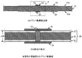
図2は、特許文献1等に記載された従来のプリント配線板における製造方法の概略を示す製造工程図である。 FIG. 2 is a manufacturing process diagram showing an outline of a manufacturing method in a conventional printed wiring board described in Patent Document 1 and the like.
従来のプリント配線板は、厚さL10の銅面板10を有している。銅面板10は、絶縁性の基材11を有し、この基材11の表面に配線パターン12が形成され、基材11の裏面に配線パターン13が形成されている。両面の配線パターン12,13の間には、スルーホール14が形成されている。スルーホール14には、金属めっき15が施され、金属めっき15を介して、基材11の両面の配線パターン12,13が電気的に接続されている。
The conventional printed wiring board has a
このような構成のプリント配線板は、例えば、以下のような工程により製造される。
先ず、図2(a)の工程において、基材11の表面に配線パターン12が形成され、裏面に配線パターン13が形成された銅面板10を用意する。
The printed wiring board having such a configuration is manufactured, for example, by the following process.
First, in the process of FIG. 2A, a
図2(b)の工程において、銅面板10に穴あけ加工を行い、スルーホール14を形成する。
In the step of FIG. 2B, the
次に、図2(c)の工程において、スルーホール14が形成された銅面板10を、金属めっき15が溶解した液体を入れためっき槽に浸す。銅面板10の配線パターン12,13を陰極として電気分解を行い、レジストによって選択された配線パターン12,13に金属めっき15を析出させる。基材11の両面の配線パターン12,13は、析出された金属めっき15を介して、電気的に接続される。その後、両面の配線パターン12,13が接続された銅面板10を、レジスト剥離液を入れた洗浄槽に浸し、レジストを剥離すれば、プリント配線板の製造が終了する。
Next, in the step of FIG. 2C, the
しかしながら、従来の図2のプリント配線板及びプリント配線板の製造方法では、以下の(1)〜(5)のような課題がある。 However, the conventional printed wiring board and the printed wiring board manufacturing method of FIG. 2 have the following problems (1) to (5).
(1) スルーホール14をドリル等で穴あけ加工するため、スルーホール14の個数が増えれば、図2(b)の工程の処理が増える。したがって、プリント配線板の製造工程において、最も時間や手間のかかる工程である。
(1) Since the
(2) 図2(b)の工程は、最も加工費が掛かる工程のため、スルーホール14の個数が増えるほど加工費も増加する。
(2) Since the process of FIG. 2B requires the highest processing cost, the processing cost increases as the number of through
(3) スルーホール14の直径が狭い、または銅面板10が厚くなると、スルーホール14に金属めっき15が施しにくくなり、めっき形成不良の原因となる。そのため、スルーホール14の断線による品質低下を招く虞がある。
(3) When the diameter of the
(4) 図2(b)の工程を行った際に切削屑がスルーホール内に残留することが多いので、切削屑を除去する洗浄工程が、図2(b)の工程と図2(c)の工程の間に必要である。 (4) Since the cutting waste often remains in the through hole when the step of FIG. 2 (b) is performed, the cleaning step for removing the cutting waste is the step of FIG. 2 (b) and FIG. 2 (c). ) During the process.
(5) 洗浄工程を行っても、切削屑が除去しきれない場合は、図2(c)の工程でスルーホール14のめっき形成不良の原因となり、スルーホール14の断線による品質低下を招く虞がある。
(5) If even if the cleaning process is performed, the cutting waste cannot be completely removed, it may cause the plating formation failure of the through
本発明のプリント配線板は、第1及び第2の配線パターンが所定の距離を隔てて形成された絶縁性の基材と、前記所定の距離に対応した長さで、前記第1及び第2の配線パターンに対し位置決めされて前記第1及び第2の配線パターンの間に打ち込まれた導電性の線状部材と、前記第1の配線パターンと前記線状部材の一端とを電気的に接続すると共に、前記第2の配線パターンと前記線状部材の他端とを電気的に接続した接続部材とを有している。 The printed wiring board of the present invention includes an insulating base material on which the first and second wiring patterns are formed at a predetermined distance, and a length corresponding to the predetermined distance, and the first and second wiring patterns. An electrically conductive linear member that is positioned with respect to the wiring pattern and is driven between the first and second wiring patterns and the first wiring pattern and one end of the linear member are electrically connected. And a connection member that electrically connects the second wiring pattern and the other end of the linear member.
本発明のプリント配線板の製造方法では、前記第1及び第2の配線パターンが前記所定の距離を隔てて形成された絶縁性の前記基材における前記第1及び第2の配線パターンに対して位置決めし、前記所定の距離に対応した長さを有する導電性の前記線状部材を前記基材に打ち込み、前記接続部材により、前記線状部材の一端と前記第1の配線パターンとを電気的に接続すると共に、前記線状部材の他端と前記第2の配線パターンとを電気的に接続する。 In the method for manufacturing a printed wiring board of the present invention, the first and second wiring patterns in the insulating base material in which the first and second wiring patterns are formed at a predetermined distance from each other. The conductive linear member having a length corresponding to the predetermined distance is driven into the substrate, and one end of the linear member and the first wiring pattern are electrically connected by the connecting member. And the other end of the linear member and the second wiring pattern are electrically connected.
本発明のプリント配線板の製造装置では、前記第1及び第2の配線パターンが前記所定の距離を隔てて形成された絶縁性の前記基材を固定するテーブルと、前記テーブルに取り付けられ、前記テーブルに固定される前記基材を過熱して軟化させるヒータと、導電性の前記線状部材を着脱自在に保持するクランパと、前記クランパを前記テーブルに対して水平方向及び垂直方向へ移動させ、且つ、前記クランパで保持する前記線状部材を中心軸として前記クランパを回転する機能を有する駆動部とを備えている。 In the printed wiring board manufacturing apparatus of the present invention, the first and second wiring patterns are attached to the table, the table fixing the insulating base material formed at a predetermined distance, A heater that overheats and softens the base material fixed to the table, a clamper that detachably holds the conductive linear member, and the clamper is moved horizontally and vertically with respect to the table, And a drive unit having a function of rotating the clamper around the linear member held by the clamper as a central axis.
本発明のプリント配線板によれば、第1及び第2の配線パターンと線状部材とを接続部材を介して接続することで、断線することなく電気的に接続できるので、品質が向上する。 According to the printed wiring board of the present invention, the first and second wiring patterns and the linear member can be electrically connected without being disconnected by connecting them via the connecting member, so that the quality is improved.
プリント配線板の製造方法によれば、プリント配線板の製造工程を簡略化でき、プリント配線板の加工費を抑えることができる。 According to the printed wiring board manufacturing method, the manufacturing process of the printed wiring board can be simplified, and the processing cost of the printed wiring board can be suppressed.
プリント配線板の製造装置によれば、前記基材への前記線状部材の打ち込みを精度よく自動的に行える。 According to the printed wiring board manufacturing apparatus, the linear member can be driven into the base material automatically and accurately.
プリント配線板は、第1及び第2の配線パターンが両面に形成された絶縁性の基材と、所定の長さで、決められた位置に打ち込まれた導電性の線状部材と、前記第1及び第2の配線パターンと前記線状部材とを電気的に接続した接続部材とを有している。 The printed wiring board includes an insulating base material on which both first and second wiring patterns are formed, a conductive linear member driven into a predetermined position at a predetermined length, and the first wiring pattern A connecting member electrically connecting the first and second wiring patterns and the linear member;
(実施例1のプリント配線板の構成)
図1(a)、(b)は、本発明の実施例1におけるプリント配線板の概略を示す断面図であり、同図(a)は、プリント配線板全体を示す図、及び、同図(b)は、同図(a)中のA部分の拡大図である。
(Configuration of Printed Wiring Board of Example 1)
FIGS. 1A and 1B are cross-sectional views schematically showing a printed wiring board according to Embodiment 1 of the present invention. FIG. 1A is a view showing the entire printed wiring board, and FIG. b) is an enlarged view of a portion A in FIG.
このプリント配線板は、厚さL20の銅面板20を有している。銅面板20は、ガラス布等で構成された絶縁性の基材21を有している。この基材21の表面21aに銅箔等で構成された第1の配線パターン22が形成され、基材21の裏面21bに銅箔等で構成された第2の配線パターン23が形成されている。
This printed wiring board has a
銅面板20には、コンピュータ援用設計(以下「CAD」という。)データの配線パターンから算出した位置に、銅等で構成された導電性の金属細線(ワイヤ)70から切断され、厚さL20に対応した長さの線状部材72が打ち込まれている。線状部材72の一端と配線パターン22は、電解めっき法等で施された銅めっき等の導電性被膜(例えば、金属めっき)24を介して電気的に接続されている。線状部材72の他端と配線パターン23は、金属めっき25を介して電気的に接続されている。
The
このプリント配線板は、例えば、チップ抵抗器や半導体集積回路等のように表面実装に適した電子部品の実装に使われ、回路の小型化が求められる電子機器等に用いられる。 This printed wiring board is used, for example, for mounting electronic components suitable for surface mounting such as chip resistors and semiconductor integrated circuits, and is used for electronic devices that require miniaturization of circuits.
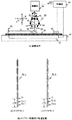
(実施例1のプリント配線板の製造装置)
図3(a)〜(c)は、図1におけるプリント配線板の製造装置の概略を示す構成図であり、同図(a)は、装置全体を示す構成図、及び、同図(b)、(c)は、ワイヤ70(=70−1または70−2)の拡大図である。
(Production apparatus for printed wiring board of Example 1)
FIGS. 3A to 3C are block diagrams showing an outline of the printed wiring board manufacturing apparatus in FIG. 1, and FIG. 3A is a block diagram showing the entire apparatus, and FIG. (C) is an enlarged view of the wire 70 (= 70-1 or 70-2).
図3(a)において、プリント配線板の製造装置は、銅面板20及びワイヤ70(=70−1または70−2)が設置され、更に、図示されていない中央処理装置(以下「CPU」という。)等で構成された制御部30を有している。この制御部30は、入力されたプログラムに基づき、制御信号S30を出力してテーブル40、カッター42及び駆動部50を制御するものである。
In FIG. 3A, the printed wiring board manufacturing apparatus is provided with a
テーブル40は、制御信号S30に基づいて、銅面板20を100℃以上の高温に加熱して軟化させるヒータ41と、テーブル40表面に載置された銅面板20を固定し、銅面板20が加熱されたときに銅面板20の反り返りを防ぐ図示されていない固定部とを有している。テーブル40の近傍には、制御信号S30に基づき、テーブル40に対して水平方向へ移動するカッター42が設置されている。このカッター42は、銅面板20の表面20aまたは裏面20bから突出したワイヤ70の突出部を切断するものである。
The table 40 fixes, based on the control signal S30, the
駆動部50は、内部構造の図示は省略するが、クランパ60をテーブル40に対して水平面のx軸方向及びこれに直交するy軸方向へ移動させるサーボーモータと、クランパ60をx,y軸方向に直交するz軸方向へ上昇または下降させるシリンダと、クランパ60を回転させるモータと、クランパ60を開閉する図示されていないばね等とにより構成されている。
Although the internal structure of the
クランパ60は、支持軸61を有し、この支持軸61の一端が駆動部50内のモータによって回転するように取り付けられている。支持軸61の他端には、開閉軸62が取り付けられ、この開閉軸62に、対向した一対のアーム部63,64の一端が取り付けられている。一対のアーム部63,64は、開閉自在でワイヤ70を挟み、他端には、対向した一対のストッパ部65,66が設けられている。ストッパ部65,66は、挟んだワイヤ70を保持するためのものである。
The
ワイヤ70には、図3(b)、(c)に示すように2種類あって、いずれか一方が使用される。
There are two types of
図3(b)において、ワイヤ70−1は、所定の長さで切断用の切り欠き71を有している。切り欠き71によって、ワイヤ70−1から線状部材72−1が構成される。線状部材72−1は、銅面板20の厚さL20に対応した長さL72で、外周面の長手方向に沿って複数の直線状のスリット73−1が形成されている。
In FIG.3 (b), the wire 70-1 has the
図3(c)において、ワイヤ70−2は、ワイヤ70−1と同様に、所定の長さで切断用の切り欠き71を有している。切り欠き71によって、ワイヤ70−2から線状部材72−2が構成される。線状部材72−2は、銅面板20の厚さL20に対応した長さL72で、外周面にスパイラル状の溝73−2が形成されている。
In FIG.3 (c), the wire 70-2 has the
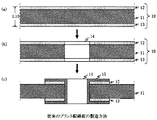
(実施例1のプリント配線板の製造方法)
図4は、図1におけるプリント配線板の製造方法の概略を示す製造工程図である。
(Method for producing printed wiring board of Example 1)
FIG. 4 is a manufacturing process diagram showing an outline of a method of manufacturing the printed wiring board in FIG.
図1におけるプリント配線板は、以下の(a)〜(d)の工程に従って製造される。
先ず、図4(a)の工程において、基材21の表面21aに配線パターン22が形成され、裏面21bに配線パターン23が形成された銅面板20と、所定の長さのワイヤ70−1と、金属めっき24,25が溶解した液体を入れた図示されていないめっき槽と、レジスト剥離液を入れた図示されていない洗浄槽とを用意する。用意した銅面板20をテーブル40に載置し、テーブル40の固定部に固定する。ワイヤ70−1を選択して、一対のアーム部63,64に挟み、一対のストッパ部65,66によって保持する。次にプリント配線板の製造装置に電源を投入し、ヒータ41を加熱し、銅面板20を軟化する。
The printed wiring board in FIG. 1 is manufactured according to the following steps (a) to (d).
First, in the step of FIG. 4A, the
図4(b)の工程において、制御信号S30により駆動部50が制御され、制御された駆動部50によりクランパ60が銅面板20からz方向に所定の高さ持ち上がる。持ち上がったクランパ60は、CADデータに基づき、銅面板20に対して水平面のx軸方向及びこれに直交するy軸方向へ移動し、基準点P1からx軸方向にXmm、y軸方向にYmm離れた打ち込み点P2の上に位置決めされる。
In the step of FIG. 4B, the
駆動部50の動作により、クランパ60がz方向に所定の圧力で降下する。この降下によって、ワイヤ70−1が打ち込み点P2に打ち込まれ、銅面板20を貫通する。制御信号S30によりカッター42が打ち込み点P2に前進して行き、切り欠き71に基づいて、ワイヤ70−1を切断し、線状部材72−1を切り離す。切断後、カッター42は、制御信号S30により原位置に復帰する。クランパ60は、駆動部50によって原位置に復帰する。固定部は、銅面板20の固定を解除する。
Due to the operation of the
図4(c)の工程において、テーブル40から線状部材72−1が打ち込まれた銅面板20を取り外し、レジスト26を塗布する。レジスト26を塗布した銅面板20を図4(a)の工程で用意しためっき槽に浸漬し、銅面板20の配線パターン22,23及び線状部材72−1を陰極として電気分解を行う。めっき槽内で電気分解を行うことにより、レジスト26によって選択された配線パターン22,23及び線状部材72−1に金属めっき24,25が析出し、析出した金属めっき24を介して、線状部材72−1の一端と配線パターン22が電気的に接続される。同様に、析出した金属めっき25を介して、線状部材72−1の他端と配線パターン23が電気的に接続される。
In the step of FIG. 4C, the
その後、図4(d)の工程において、銅面板20を図4(a)の工程で用意したレジスト除去槽に浸漬し、レジスト26を剥離すれば、プリント配線板の製造が終了する。
Thereafter, in the step of FIG. 4D, the
(実施例1の他のプリント配線板の製造方法)
実施例1の他のプリント配線板の製造方法では、図4(b)の工程において図3(c)のワイヤ70−2を用いた方法を説明する。
(Manufacturing method of another printed wiring board of Example 1)
In another printed wiring board manufacturing method of the first embodiment, a method using the wire 70-2 of FIG. 3C in the step of FIG. 4B will be described.
ワイヤ70−2を選択して、一対のアーム部63,64に挟み、一対のストッパ部65,66によって保持する。ワイヤ70−1を用いた場合と同様に電源投入し、位置決めを行う。クランパ60がz方向に所定の圧力で降下するさいに、駆動部50によって、支持軸61が回転される。支持軸61の回転によって、ワイヤ70−2が回転しながら打ち込み点P2に打ち込まれ、銅面板20を貫通する。貫通後の処理は、ワイヤ70−1を用いた場合と同様である。
The wire 70-2 is selected, sandwiched between the pair of
(実施例1の効果)
本実施例1によれば、次の(1)〜(3)のような効果がある。
(Effect of Example 1)
According to the first embodiment, there are the following effects (1) to (3).
(1) 本実施例1のプリント配線板によれば、スルーホールに代えて、ワイヤ72を用いている。そのため配線パターン22,23が金属めっき24,25によって確実に接続されるので、断線することなく接続できるので、品質が向上する。
(1) According to the printed wiring board of the first embodiment, the
(2) 本実施例1のプリント配線板の製造方法によれば、銅面板20を加熱して軟化するので、厚さL20が厚くなっても少ない圧力でワイヤ72を打ち込むことができる。また、ワイヤ72を打ち込むようにしたので、切削屑がなくなり、洗浄工程が不要となる。更に、プリント配線板の製造工程の簡略化を図ることができる。スルーホールを形成する穴あけ加工、穴あけ加工時に出る切削屑の洗浄、スルーホールのみに金属めっきを施すめっき処理を省略できるので、プリント配線板の製造時間が短縮でき、プリント配線板の加工費を抑えることができる。
(2) According to the printed wiring board manufacturing method of the first embodiment, since the
(3) 本実施例1のプリント配線板の製造装置によれば、銅面板20へのワイヤ70の打ち込みを精度よく自動的に行える。
(3) According to the printed wiring board manufacturing apparatus of the first embodiment, the
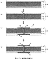
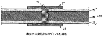
(実施例2のプリント配線板の構成)
図5は、本発明の実施例2におけるプリント配線板の概略を示す断面図であり、実施例1を示す図1中の要素と共通の要素には、共通の符号が付されている。
(Configuration of Printed Wiring Board of Example 2)
FIG. 5 is a cross-sectional view schematically illustrating a printed wiring board according to the second embodiment of the present invention. Elements common to those in FIG. 1 illustrating the first embodiment are denoted by common reference numerals.
この実施例2のプリント配線板は、実施例1のプリント配線板との相違点として、配線パターン22,23及び線状部材72の接続に金属めっき24,25に代えて、銀やはんだ等の導電(例えば、熱硬化型)ペースト27,28を使用している。
The printed wiring board according to the second embodiment is different from the printed wiring board according to the first embodiment in that, instead of the metal plating 24 and 25 for connecting the
(実施例2のプリント配線板の製造方法)
実施例2のプリント配線板の製造方法では、実施例1のプリント配線板の製造方法と比べて、金属めっき24,25に代えて熱硬化型ペースト27,28を用いたので、図4の(c)の工程が異なる。
(Manufacturing method of the printed wiring board of Example 2)
In the printed wiring board manufacturing method of the second embodiment, compared with the printed wiring board manufacturing method of the first embodiment, the thermosetting pastes 27 and 28 are used instead of the metal plating 24 and 25. The process of c) is different.
即ち、銅面板20に線状部材72を打ち込んだ後に、スクリーン印刷等によって選択された配線パターン22とワイヤ24の一端とに熱硬化型ペースト27を塗布し、同様に配線パターン23とワイヤ24の他端とに熱硬化型ペースト28を塗布する。熱硬化型ペースト27,28を塗布した銅面板20をリフロー炉に通し、熱硬化型ペースト27,28を150〜180℃に加熱して硬化する。
That is, after the
硬化した熱硬化型ペースト27を介して、線状部材72の一端と配線パターン22が電気的に接続される。同様に、硬化された熱硬化型ペースト28を介して、線状部材72の他端と配線パターン23が電気的に接続される。レジスト26を使用していないので、レジスト26の剥離を行わずにプリント配線板の製造が終了する。
One end of the
(実施例2の効果)
本実施例2によれば、実施例1の金属めっき24,25に代えて、熱硬化型ペースト27,28を用いたことで、実施例1と同様の効果に加えて、以下のような効果がある。
(Effect of Example 2)
According to the second embodiment, by using the thermosetting pastes 27 and 28 in place of the
レジスト26の剥離を行わなくてよいので、処理を省略できる。そのため、プリント配線板の製造時間が短縮でき、プリント配線板の加工費を抑えることができる。 Since it is not necessary to remove the resist 26, the processing can be omitted. Therefore, the manufacturing time of a printed wiring board can be shortened and the processing cost of a printed wiring board can be suppressed.
(変形例)
本発明は、上記実施例1、2に限定されず、種々の利用形態や変形が可能である。この利用形態や変形例としては、例えば、次の(1)〜(6)のようなものがある。
(Modification)
The present invention is not limited to the first and second embodiments, and various usage forms and modifications are possible. For example, the following forms (1) to (6) are used as the usage form and the modification examples.
(1) 実施例1、2では、プリント配線板に基材21の両面に配線パターン22,23が形成されたプリント配線板を用いたが、プリント配線板を複数積層した多層プリント配線板、フレキシブルプリント印刷板を用いてもよい。
(1) In the first and second embodiments, the printed wiring board in which the
(2) 実施例1では、予め配線パターン22,23が形成された基材21に線状部材72を打ち込んだが、配線パターン22,23の形成前の銅面板20に線状部材72を打ち込み、それから配線パターン22,23を形成してもよい。
(2) In Example 1, the
(3) 実施例2では、銅面板20にワイヤ70を打ち込んだ後に、熱硬化型ペースト27,28を塗布し、配線パターン22,23と線状部材72の接続を行ったが、プリント配線基板へ部品実装を行うときに、配線パターン22,23と線状部材72の接続を行ってもよい。
(3) In Example 2, after the
(4) 実施例1、2では、テーブル40近傍のカッター42でワイヤ70から線状部材72を切り離したが、ストッパ部65,66に切断機能をもたせ、挟み込み加圧することでワイヤ70を切断してもよい。カッター42の切断処理、原位置への復帰動作がなくなるので、プリント配線板の製造時間が短縮できる。
(4) In the first and second embodiments, the
(5) 実施例1、2では、駆動部50によって、クランパ60がテーブル40に対して水平面のx軸方向及びこれに直交するy軸方向に移動したが、テーブル40がクランパ60に対して相対的に移動してもよい。
(5) In Embodiments 1 and 2, the
(6) 実施例1、2では、線状部材72の外周面に直線状のスリット73−1またはスパイラル状の溝73−2が形成してあったが、形成しなくてもよい。スリット73−1または溝73−2を形成しないことで、線状部材72の加工費が安くなる。
(6) In the first and second embodiments, the linear slit 73-1 or the spiral groove 73-2 is formed on the outer peripheral surface of the
11,21 基材
12,13,22,23 配線パターン
15,24,25 金属めっき
27,28 熱硬化型ペースト
40 テーブル
41 ヒータ
50 駆動部
60 クランパ
70 ワイヤ
72 線状部材
11,21
Claims (9)
前記所定の距離に対応した長さで、前記第1及び第2の配線パターンに対し位置決めされて前記第1及び第2の配線パターンの間に打ち込まれた導電性の線状部材と、
前記第1の配線パターンと前記線状部材の一端とを電気的に接続すると共に、前記第2の配線パターンと前記線状部材の他端とを電気的に接続した接続部材と、
を有することを特徴とするプリント配線板。 An insulating substrate in which the first and second wiring patterns are formed at a predetermined distance; and
A conductive linear member that is positioned with respect to the first and second wiring patterns and is driven between the first and second wiring patterns with a length corresponding to the predetermined distance;
A connection member that electrically connects the first wiring pattern and one end of the linear member, and electrically connects the second wiring pattern and the other end of the linear member;
A printed wiring board comprising:
前記所定の距離に対応した長さを有する導電性の線状部材を前記基材に打ち込み、
接続部材により、前記線状部材の一端と前記第1の配線パターンとを電気的に接続すると共に、前記線状部材の他端と前記第2の配線パターンとを電気的に接続することを特徴とするプリント配線板の製造方法。 The first and second wiring patterns are positioned with respect to the first and second wiring patterns in an insulating base material formed at a predetermined distance,
A conductive linear member having a length corresponding to the predetermined distance is driven into the base material,
A connecting member electrically connects one end of the linear member and the first wiring pattern, and electrically connects the other end of the linear member and the second wiring pattern. A method for manufacturing a printed wiring board.
前記テーブルに取り付けられ、前記テーブルに固定される前記基材を過熱して軟化させるヒータと、
導電性の線状部材を着脱自在に保持するクランパと、
前記クランパを前記テーブルに対して水平方向及び垂直方向へ移動させ、且つ、前記クランパで保持する前記線状部材を中心軸として前記クランパを回転する機能を有する駆動部と、
を備えたことを特徴とするプリント配線板の製造装置。 A table for fixing an insulating base material on which the first and second wiring patterns are formed at a predetermined distance;
A heater attached to the table and overheating and softening the base material fixed to the table;
A clamper for detachably holding a conductive linear member;
A drive unit having a function of moving the clamper in a horizontal direction and a vertical direction with respect to the table, and rotating the clamper about the linear member held by the clamper as a central axis;
An apparatus for producing a printed wiring board, comprising:
Priority Applications (1)
| Application Number | Priority Date | Filing Date | Title |
|---|---|---|---|
| JP2006351465A JP2008166350A (en) | 2006-12-27 | 2006-12-27 | Printed circuit board, apparatus and method for manufacturing printed circuit board |
Applications Claiming Priority (1)
| Application Number | Priority Date | Filing Date | Title |
|---|---|---|---|
| JP2006351465A JP2008166350A (en) | 2006-12-27 | 2006-12-27 | Printed circuit board, apparatus and method for manufacturing printed circuit board |
Publications (1)
| Publication Number | Publication Date |
|---|---|
| JP2008166350A true JP2008166350A (en) | 2008-07-17 |
Family
ID=39695482
Family Applications (1)
| Application Number | Title | Priority Date | Filing Date |
|---|---|---|---|
| JP2006351465A Withdrawn JP2008166350A (en) | 2006-12-27 | 2006-12-27 | Printed circuit board, apparatus and method for manufacturing printed circuit board |
Country Status (1)
| Country | Link |
|---|---|
| JP (1) | JP2008166350A (en) |
Cited By (1)
| Publication number | Priority date | Publication date | Assignee | Title |
|---|---|---|---|---|
| EP2139014A2 (en) | 2008-06-25 | 2009-12-30 | Alps Electric Co., Ltd. | Push switch and method of manufacturing the same |
-
2006
- 2006-12-27 JP JP2006351465A patent/JP2008166350A/en not_active Withdrawn
Cited By (1)
| Publication number | Priority date | Publication date | Assignee | Title |
|---|---|---|---|---|
| EP2139014A2 (en) | 2008-06-25 | 2009-12-30 | Alps Electric Co., Ltd. | Push switch and method of manufacturing the same |
Similar Documents
| Publication | Publication Date | Title |
|---|---|---|
| US7799603B2 (en) | Method for mounting electronic component on printed circuit board | |
| CN112203426A (en) | Back drilling method, device and equipment for printed circuit board and storage medium | |
| CN113597113A (en) | Manufacturing method of high-reflectivity white oil circuit board | |
| CN100551206C (en) | Make the method for rigid-flexible printed circuit board | |
| KR102873275B1 (en) | Method for manufacturing flexible printed circuit board | |
| CN113473717A (en) | Method for manufacturing circuit board solder resist pattern in partition mode | |
| KR20050001029A (en) | Method for manufacturing double side a flexible printed circuit board | |
| KR100826344B1 (en) | Substrate Laser Drilling Scanning Method | |
| JP2008166350A (en) | Printed circuit board, apparatus and method for manufacturing printed circuit board | |
| JP2008130748A (en) | Method of manufacturing printed circuit board containing resistive element | |
| JP5317491B2 (en) | Method for manufacturing printed wiring board | |
| JP2010212372A (en) | Method of manufacturing card edge terminal of printed wiring board | |
| CN103974563A (en) | PTH plating method of printed circuit boards | |
| KR20080061816A (en) | Printed circuit board and manufacturing method thereof | |
| CN105307405A (en) | Method for making circuit board by polyimide etching | |
| KR20110110664A (en) | Manufacturing method of double-sided printed circuit board | |
| KR100814710B1 (en) | Copper foil etched printed circuit board and its manufacturing method | |
| KR20130044554A (en) | Printed circuit board and manufacturing method therefor | |
| CN108617105B (en) | A PCB production process with lead electroplating inside the board | |
| JP2700259B2 (en) | Method of forming solder layer having recess in printed wiring board | |
| JP4705972B2 (en) | Printed wiring board and manufacturing method thereof | |
| CN115250574A (en) | Manufacturing method of circuit board and drilling device | |
| CN105228349B (en) | A method of improve without golden on copper hole | |
| KR20150059358A (en) | method for manufacturing a printed circuit board | |
| JPH06296076A (en) | Side face electrode forming method of smd module |
Legal Events
| Date | Code | Title | Description |
|---|---|---|---|
| A300 | Withdrawal of application because of no request for examination |
Free format text: JAPANESE INTERMEDIATE CODE: A300 Effective date: 20100302 |