JP2008051964A - Optical film cutting method and optical film - Google Patents
Optical film cutting method and optical film Download PDFInfo
- Publication number
- JP2008051964A JP2008051964A JP2006226870A JP2006226870A JP2008051964A JP 2008051964 A JP2008051964 A JP 2008051964A JP 2006226870 A JP2006226870 A JP 2006226870A JP 2006226870 A JP2006226870 A JP 2006226870A JP 2008051964 A JP2008051964 A JP 2008051964A
- Authority
- JP
- Japan
- Prior art keywords
- optical film
- film
- laser beam
- cut
- cutting
- Prior art date
- Legal status (The legal status is an assumption and is not a legal conclusion. Google has not performed a legal analysis and makes no representation as to the accuracy of the status listed.)
- Granted
Links
Images

Classifications
-
- B—PERFORMING OPERATIONS; TRANSPORTING
- B23—MACHINE TOOLS; METAL-WORKING NOT OTHERWISE PROVIDED FOR
- B23K—SOLDERING OR UNSOLDERING; WELDING; CLADDING OR PLATING BY SOLDERING OR WELDING; CUTTING BY APPLYING HEAT LOCALLY, e.g. FLAME CUTTING; WORKING BY LASER BEAM
- B23K26/00—Working by laser beam, e.g. welding, cutting or boring
- B23K26/36—Removing material
- B23K26/38—Removing material by boring or cutting
-
- B—PERFORMING OPERATIONS; TRANSPORTING
- B23—MACHINE TOOLS; METAL-WORKING NOT OTHERWISE PROVIDED FOR
- B23K—SOLDERING OR UNSOLDERING; WELDING; CLADDING OR PLATING BY SOLDERING OR WELDING; CUTTING BY APPLYING HEAT LOCALLY, e.g. FLAME CUTTING; WORKING BY LASER BEAM
- B23K26/00—Working by laser beam, e.g. welding, cutting or boring
- B23K26/36—Removing material
- B23K26/40—Removing material taking account of the properties of the material involved
- B23K26/402—Removing material taking account of the properties of the material involved involving non-metallic material, e.g. isolators
-
- G—PHYSICS
- G02—OPTICS
- G02B—OPTICAL ELEMENTS, SYSTEMS OR APPARATUS
- G02B5/00—Optical elements other than lenses
- G02B5/30—Polarising elements
-
- H—ELECTRICITY
- H01—ELECTRIC ELEMENTS
- H01S—DEVICES USING THE PROCESS OF LIGHT AMPLIFICATION BY STIMULATED EMISSION OF RADIATION [LASER] TO AMPLIFY OR GENERATE LIGHT; DEVICES USING STIMULATED EMISSION OF ELECTROMAGNETIC RADIATION IN WAVE RANGES OTHER THAN OPTICAL
- H01S3/00—Lasers, i.e. devices using stimulated emission of electromagnetic radiation in the infrared, visible or ultraviolet wave range
-
- B—PERFORMING OPERATIONS; TRANSPORTING
- B23—MACHINE TOOLS; METAL-WORKING NOT OTHERWISE PROVIDED FOR
- B23K—SOLDERING OR UNSOLDERING; WELDING; CLADDING OR PLATING BY SOLDERING OR WELDING; CUTTING BY APPLYING HEAT LOCALLY, e.g. FLAME CUTTING; WORKING BY LASER BEAM
- B23K2101/00—Articles made by soldering, welding or cutting
- B23K2101/18—Sheet panels
-
- B—PERFORMING OPERATIONS; TRANSPORTING
- B23—MACHINE TOOLS; METAL-WORKING NOT OTHERWISE PROVIDED FOR
- B23K—SOLDERING OR UNSOLDERING; WELDING; CLADDING OR PLATING BY SOLDERING OR WELDING; CUTTING BY APPLYING HEAT LOCALLY, e.g. FLAME CUTTING; WORKING BY LASER BEAM
- B23K2103/00—Materials to be soldered, welded or cut
- B23K2103/16—Composite materials, e.g. fibre reinforced
- B23K2103/166—Multilayered materials
- B23K2103/172—Multilayered materials wherein at least one of the layers is non-metallic
-
- B—PERFORMING OPERATIONS; TRANSPORTING
- B23—MACHINE TOOLS; METAL-WORKING NOT OTHERWISE PROVIDED FOR
- B23K—SOLDERING OR UNSOLDERING; WELDING; CLADDING OR PLATING BY SOLDERING OR WELDING; CUTTING BY APPLYING HEAT LOCALLY, e.g. FLAME CUTTING; WORKING BY LASER BEAM
- B23K2103/00—Materials to be soldered, welded or cut
- B23K2103/30—Organic material
- B23K2103/42—Plastics
-
- B—PERFORMING OPERATIONS; TRANSPORTING
- B23—MACHINE TOOLS; METAL-WORKING NOT OTHERWISE PROVIDED FOR
- B23K—SOLDERING OR UNSOLDERING; WELDING; CLADDING OR PLATING BY SOLDERING OR WELDING; CUTTING BY APPLYING HEAT LOCALLY, e.g. FLAME CUTTING; WORKING BY LASER BEAM
- B23K2103/00—Materials to be soldered, welded or cut
- B23K2103/50—Inorganic material, e.g. metals, not provided for in B23K2103/02 – B23K2103/26
Landscapes
- Engineering & Computer Science (AREA)
- Physics & Mathematics (AREA)
- Optics & Photonics (AREA)
- Plasma & Fusion (AREA)
- Mechanical Engineering (AREA)
- Electromagnetism (AREA)
- General Physics & Mathematics (AREA)
- Polarising Elements (AREA)
Abstract
【課題】レーザビームがガウシアンビームの特性を有する場合であっても、レーザビームが照射される単位長さ当たりのエネルギ及び連続照射時間を制御したレーザビームを使用して偏光フィルム等の光学フィルムを切断することにより、光学フィルムの切断面における盛り上がりサイズを可及的に小さくすることが可能であり、もって各種の光学パネルに組み込んだ際に接着不良や光学的不具合が発生することを防止可能な光学フィルムの切断方法及びその切断方法により切断された光学フィルムを提供する。
【解決手段】単位長さ当たりのエネルギが0.12〜0.167J/mmであり且つ連続照射時間が0.1msec以下の条件で、レーザビームを光学フィルムに照射して光学フィルムを切断するように構成する。
【選択図】図2An optical film such as a polarizing film is produced using a laser beam in which the energy per unit length irradiated with the laser beam and the continuous irradiation time are controlled even when the laser beam has the characteristics of a Gaussian beam. By cutting, it is possible to reduce the rising size on the cut surface of the optical film as much as possible, and thus it is possible to prevent the occurrence of poor adhesion and optical defects when incorporated in various optical panels. An optical film cutting method and an optical film cut by the cutting method are provided.
The optical film is cut by irradiating the optical film with a laser beam under the condition that the energy per unit length is 0.12 to 0.167 J / mm and the continuous irradiation time is 0.1 msec or less. Configure.
[Selection] Figure 2
Description
本発明は、レーザビームを使用して光学フィルムを切断する方法及びその切断方法により得られる光学フィルムに関し、特に、レーザビームにおける単位長さ当たりのエネルギ及び連続照射時間を制御したレーザビームを使用して偏光フィルム等の光学フィルムの切断を行う光学フィルムの切断方法及びその切断方法により切断された光学フィルムに関するものである。 The present invention relates to a method of cutting an optical film using a laser beam and an optical film obtained by the cutting method, and more particularly, to use a laser beam with controlled energy per unit length and continuous irradiation time in the laser beam. The present invention relates to an optical film cutting method for cutting an optical film such as a polarizing film, and an optical film cut by the cutting method.
従来より、偏光フィルム等の各種の光学フィルムを切断するについては、金型や切断刃を使用して切断する機械式切断方法や光学フィルムにレーザビームを照射して切断するレーザ切断方法が存在する。 Conventionally, for cutting various optical films such as polarizing films, there are mechanical cutting methods for cutting using a mold or a cutting blade, and laser cutting methods for cutting an optical film by irradiating it with a laser beam. .
ここに、機械式切断方法は、光学フィルムを切断する際に切断面から微細な切断カスが発生し、かかる切断カスは、光学フィルムを液晶パネル等に実装する際に、液晶パネル内部に混入してしまう場合がある。このように液晶パネル内部に切断カスが混入してしまうと、液晶パネルによる表示上不具合が発生することから、結果的に液晶パネルの製造上歩留まりが低下してしまうという問題がある。 Here, in the mechanical cutting method, when cutting the optical film, a fine cutting residue is generated from the cut surface, and this cutting residue is mixed inside the liquid crystal panel when the optical film is mounted on the liquid crystal panel or the like. May end up. If the cutting residue is mixed in the liquid crystal panel in this manner, a display defect due to the liquid crystal panel occurs, resulting in a problem that the manufacturing yield of the liquid crystal panel is lowered.
これに対して、レーザ切断方法の場合には、光学フィルムの切断時に切断カスが発生し難いことから、前記した機械式切断方法に比べて液晶パネル等の製造時に歩留まりがそれ程低下してしまうことはなく、機械式切断方法よりも優れた切断方法である。 On the other hand, in the case of the laser cutting method, since the cutting residue is less likely to be generated when the optical film is cut, the yield is much reduced during the manufacture of the liquid crystal panel or the like as compared with the mechanical cutting method described above. It is a cutting method superior to the mechanical cutting method.
例えば、特開2005−189530には、偏光板と光透過率が80%以上であり且つガラス転移温度が100℃以上である樹脂フィルムとを積層して積層体を形成し、かかる積層体の樹脂フィルム側にレーザを照射することによって、積層体を切断する積層型偏光板の製造方法が記載されている。
前記積層型偏光板の製造方法によれば、偏光板と樹脂フィルムとの積層体における樹脂フィルム側にレーザを照射することにより、偏光板の切断面において突起物や隆起の発生を防止することができるものである。
For example, in JP-A-2005-189530, a laminate is formed by laminating a polarizing plate and a resin film having a light transmittance of 80% or more and a glass transition temperature of 100 ° C. or more. A manufacturing method of a laminated polarizing plate is described in which a laminated body is cut by irradiating a laser on the film side.
According to the method for producing a laminated polarizing plate, by irradiating a laser on the resin film side in the laminate of the polarizing plate and the resin film, it is possible to prevent the occurrence of protrusions and protrusions on the cut surface of the polarizing plate. It can be done.
しかしながら、前記積層型偏光板の製造方法において使用されるレーザは、一般に、ガウシアンビーム(ビーム強度がガウス分布しているビーム)である。かかるガウシアンビームは、ビーム強度がガウス分布していることから、ビームスポットの中心部におけるビーム強度は大きいが、中心部から外側にいくに従って徐々にビーム強度が小さくなっていく特性を有している。 However, the laser used in the method for manufacturing the laminated polarizing plate is generally a Gaussian beam (a beam having a Gaussian distribution of beam intensity). Since the Gaussian beam has a Gaussian distribution, the beam intensity at the center of the beam spot is large, but the beam intensity gradually decreases from the center to the outside. .
従って、前記したガウシアンビームを使用して光学フィルムを切断すると、先ずビームスポットの中心部で光学フィルム成分の分解気化が発生して切断されていくものの、ビームスポットの中心部の外側にいくに従ってビーム強度が小さくなっていくことから、光学フィルム成分の分解は徐々に溶融、分解されていくこととなる。 Therefore, when the optical film is cut by using the Gaussian beam, the optical film component is first decomposed and vaporized at the center of the beam spot, but the beam is moved toward the outside of the center of the beam spot. Since the strength is reduced, the decomposition of the optical film component is gradually melted and decomposed.
このとき、ビームスポットの中心部で光学フィルム成分が分解気化される際に外側に向かう応力が発生し、かかる応力に起因してビームスポットの中心部の外側では、未だ分解気化せず溶融されたままの光学フィルム成分が外側に押しやられる。この結果、光学フィルムの切断面には、その溶融成分の突起部(盛り上がり部)が発生してしまう。 At this time, when the optical film component is decomposed and vaporized at the center portion of the beam spot, an outward stress is generated, and due to the stress, the outer portion of the beam spot is melted without being decomposed and vaporized. The remaining optical film component is pushed outward. As a result, a projection (swelled portion) of the molten component occurs on the cut surface of the optical film.
前記のように発生した光学フィルム切断面に盛り上がり部が発生すると、光学フィルムを液晶パネル等に組み込む際に、液晶パネルの端縁部で接着不良等が発生したり、また、光学的にも各種の不具合が発生してしまう問題がある。 When a raised part occurs on the cut surface of the optical film generated as described above, when the optical film is incorporated into a liquid crystal panel or the like, adhesion failure or the like occurs at the edge of the liquid crystal panel. There is a problem that this problem occurs.
本発明は前記従来における問題点を解消するためになされたものであり、レーザビームがガウシアンビームの特性を有する場合であっても、レーザビームにおける単位長さ当たりのエネルギ及び連続照射時間を制御したレーザビームを使用して偏光フィルム等の光学フィルムを切断することにより、光学フィルムの切断面における盛り上がりサイズを可及的に小さくすることが可能であり、もって各種の光学パネルに組み込んだ際に接着不良や光学的不具合が発生することを防止可能な光学フィルムの切断方法及びその切断方法により切断された光学フィルムを提供することを目的とする。 The present invention has been made to solve the above-described conventional problems, and even when the laser beam has the characteristics of a Gaussian beam, the energy per unit length and the continuous irradiation time in the laser beam are controlled. By cutting an optical film such as a polarizing film using a laser beam, it is possible to reduce the rising size of the cut surface of the optical film as much as possible. An object of the present invention is to provide an optical film cutting method capable of preventing the occurrence of defects and optical defects, and an optical film cut by the cutting method.
前記目的を達成するため請求項1に係る光学フィルムの切断方法は、単位長さ当たりのエネルギが0.12〜0.167J/mmであり且つ連続照射時間が0.1msec以下の条件で、レーザビームを光学フィルムに照射して光学フィルムを切断することを特徴とする。 In order to achieve the above object, the method for cutting an optical film according to claim 1 is based on the condition that the energy per unit length is 0.12 to 0.167 J / mm and the continuous irradiation time is 0.1 msec or less. The optical film is irradiated with a beam to cut the optical film.
請求項2に係る光学フィルムの切断方法は、請求項1の切断方法において、前記レーザビームにより光学フィルムを切断する際にフィルム切断面に発生する盛り上がり部は、30μm以下であることを特徴とする。
The optical film cutting method according to
請求項3に係る光学フィルムは、請求項1のレーザビームにより切断され、その切断面に発生する盛り上がり部が30μm以下であることを特徴とする。
The optical film according to
請求項1の光学フィルムの切断方法によれば、単位長さ当たりのエネルギが0.12〜0.167J/mmであり且つ連続照射時間が0.1msec以下の条件で、レーザビームを光学フィルムに照射して光学フィルムを切断するので、レーザビームがガウシアンビームの特性を有する場合であっても、光学フィルムの切断面における盛り上がりサイズを可及的に小さくすることが可能であり、これより各種の光学パネルに組み込んだ際に接着不良や光学的不具合が発生することを防止可能となる。 According to the method for cutting an optical film of claim 1, the laser beam is applied to the optical film under the condition that the energy per unit length is 0.12 to 0.167 J / mm and the continuous irradiation time is 0.1 msec or less. Since the optical film is cut by irradiation, even if the laser beam has the characteristics of a Gaussian beam, it is possible to reduce the rising size on the cut surface of the optical film as much as possible. It becomes possible to prevent the occurrence of poor adhesion or optical failure when incorporated in an optical panel.
ここに、前記したレーザビームを使用する切断方法によれば、切断面に発生する盛り上がり部を30μm以下にした光学フィルムを得ることができる。 Here, according to the cutting method using the laser beam described above, it is possible to obtain an optical film having a raised portion generated on the cut surface of 30 μm or less.
以下、本発明に係る光学フィルムの切断方法について、実施形態に基づき図面を参照しつつ詳細に説明する。
先ず、本実施形態に係る光学フィルムの構成について図1に基づき説明する。図1は光学フィルムの構成を模式的に示す説明図である。
Hereinafter, the cutting method of the optical film which concerns on this invention is demonstrated in detail, referring drawings based on embodiment.
First, the structure of the optical film which concerns on this embodiment is demonstrated based on FIG. FIG. 1 is an explanatory view schematically showing the structure of an optical film.
図1において、光学フィルム1は、基本的に、偏光板2、偏光板2の上面に接着された表面保護フィルム3、偏光板2の下面に粘着剤層4を介して接着されたセパレータ5から構成される。
In FIG. 1, an optical film 1 basically includes a polarizing
ここに、偏光板2としては従来公知のものが使用でき、一般に、偏光フィルムの片面又は両面に透明保護層が形成されたものがあげられる。前記偏光フィルムとしては特に制限されず、従来公知の偏光フィルムが使用できる。具体的には、例えば、従来公知の方法により、各種フィルムに、ヨウ素や二色性染料等の二色性物質を吸着させて染色し、架橋、延伸、乾燥することによって調製したもの等が使用できる。この中でも、自然光を入射させると直線偏光を透過するフィルムが好ましく、光透過率や偏光度に優れるものが好ましい。前記二色性物質を吸着させる各種フィルムとしては、例えば、PVA系フィルム、部分ホルマール化PVA系フィルム、エチレン・酢酸ビニル共重合体系部分ケン化フィルム、セルロース系フィルム等の親水性高分子フィルム等があげられ、これらの他にも、例えば、PVAの脱水処理物やポリ塩化ビニルの脱塩酸処理物等のポリエン配向フィルム等も使用できる。これらの中でも、好ましくはPVA系フィルムである。また、前記偏光フィルムの厚さは、通常、200μm程度であるが、これには限定されない。
Here, as the polarizing
前記透明保護層としては、特に制限されず、従来公知の透明フィルムを使用できるが、例えば、透明性、機械的強度、熱安定性、水分遮断性、等方性などに優れるものが好ましい。このような透明保護層の材質の具体例としては、ポリエチレンテレフタレート、ポリエチレンナフタレート等のポリエステル系ポリマー、ジアセチルセルロースやトリアセチルセルロース等のセルロース系ポリマー、ポリメチル(メタ)アクリレートのアクリル系ポリマー、ポリスチレンやアクリルニトリル・スチレン共重合体(AS樹脂)等のスチレン系ポリマー、ポリカーボネート系ポリマー等が挙げられる。また、ポリエチレン、ポリプロピレン、シクロ系またはノルボルネン構造を有するポリオレフィン、エチレン・プロピレン共重合体等のポリオレフィン系ポリマー、塩化ビニルポリマー、ナイロンや芳香族ポリアミド系ポリマー、イミド系ポリマー、スルフォン系ポリマー、ポリエーテルスルフォン系ポリマー、ポリエーテルエーテルケトン系ポリマー、塩化ビニリデン系ポリマー、ビニルアルコール系ポリマー、ビニルブチラール系ポリマー、アリレート系ポリマー、ポリオキシメチレン系ポリマー、エポキシ系ポリマー、前記各種ポリマーのブレンド物等があげられる。中でもセルロース系ポリマーが好ましい。透明保護フィルムの厚さは特に限定はない。 The transparent protective layer is not particularly limited, and a conventionally known transparent film can be used. For example, a layer having excellent transparency, mechanical strength, thermal stability, moisture barrier property, isotropy, and the like is preferable. Specific examples of the material for such a transparent protective layer include polyester polymers such as polyethylene terephthalate and polyethylene naphthalate, cellulose polymers such as diacetyl cellulose and triacetyl cellulose, acrylic polymers of polymethyl (meth) acrylate, polystyrene and the like. Examples thereof include styrene polymers such as acrylonitrile / styrene copolymer (AS resin), polycarbonate polymers, and the like. In addition, polyethylene, polypropylene, polyolefin having a cyclo or norbornene structure, polyolefin polymer such as ethylene / propylene copolymer, vinyl chloride polymer, nylon or aromatic polyamide polymer, imide polymer, sulfone polymer, polyether sulfone Polymers, polyether ether ketone polymers, vinylidene chloride polymers, vinyl alcohol polymers, vinyl butyral polymers, arylate polymers, polyoxymethylene polymers, epoxy polymers, blends of the above-mentioned various polymers, and the like. Of these, cellulosic polymers are preferred. The thickness of the transparent protective film is not particularly limited.
前記偏光フィルムと透明保護層との接着は、特に制限されないが、例えば、イソシアネート系接着剤、ポリビニルアルコール系接着剤、ゼラチン系接着剤、ビニル系ラテックス系、水系プロエステル等が使用できる。 Adhesion between the polarizing film and the transparent protective layer is not particularly limited, and for example, an isocyanate adhesive, a polyvinyl alcohol adhesive, a gelatin adhesive, a vinyl latex, an aqueous proester, or the like can be used.
前記偏光板2の表面には、例えば、ハードコート処理、反射防止処理、スティッキング防止処理、拡散処理、アンチグレア処理、反射防止つきアンチグレア処理、帯電防止処理、汚染防止処理等の種々の処理を目的に応じて施してもよい。 For the purpose of various treatments such as hard coat treatment, antireflection treatment, antisticking treatment, diffusion treatment, antiglare treatment, antiglare treatment with antireflection, antistatic treatment, antifouling treatment, etc. It may be given accordingly.
前記ハードコート処理は、偏光板表面の傷つき防止などを目的とし、例えば、アクリル系、シリコーン系等の紫外線硬化型樹脂により、硬度やすべり特性に優れる硬化皮膜をフィルムの表面に形成する方法によって行うことができる。前記反射防止処理は、光学フィルム表面での外光の反射防止を目的とし、従来公知の反射防止膜(物理光学薄膜、塗工薄膜)等の形成により行うことができる。 The hard coat treatment is performed for the purpose of preventing scratches on the surface of the polarizing plate, for example, by a method of forming a cured film having excellent hardness and slip properties on the surface of the film with an ultraviolet-curing resin such as acrylic or silicone. be able to. The antireflection treatment is performed for the purpose of preventing reflection of external light on the surface of the optical film, and can be performed by forming a conventionally known antireflection film (physical optical thin film, coating thin film) or the like.
また、アンチグレア処理は、光学フィルム表面で外光が反射して偏光板透過光の視認性を阻害することの防止等を目的とする。例えば、サンドブラスト方式、エンボス加工方式等によるフィルムの疎面化や、フィルム形成材料に透明微粒子を配合する成膜方法等によって、フィルム表面へ微細凹凸構造を付与すればよい。前記表面微細凹凸の形成に含有させる微粒子としては、平均粒径が、例えば、0.5〜50μmであり、シリカ、アルミナ、チタニア、ジルコニア、酸化錫、酸化インジウム、酸化カドミウム、酸化アンチモン等の有機系材料から構成された透明微粒子等が使用できる。表面微細凹凸構造を形成する場合、微粒子の使用量は、樹脂100重量部に対して、一般的に2〜50重量部程度であり、好ましくは5〜25重量部である。アンチグレア層は、偏光板透過光を拡散して視覚などを拡大するための拡散層(視覚拡大機能など)を兼ねるものであっても良い。 The anti-glare treatment is intended to prevent the external light from being reflected on the surface of the optical film and preventing the visibility of the light transmitted through the polarizing plate from being impaired. For example, a fine concavo-convex structure may be imparted to the film surface by thinning the film by a sandblasting method, an embossing method, or the like, or by a film forming method in which transparent fine particles are blended in a film forming material. The fine particles to be included in the formation of the fine surface irregularities have an average particle size of, for example, 0.5 to 50 μm, and are organic such as silica, alumina, titania, zirconia, tin oxide, indium oxide, cadmium oxide, and antimony oxide. Transparent fine particles composed of a system material can be used. When forming a fine surface relief structure, the amount of fine particles used is generally about 2 to 50 parts by weight, preferably 5 to 25 parts by weight, per 100 parts by weight of the resin. The anti-glare layer may also serve as a diffusion layer (such as a visual enlargement function) for diffusing the light transmitted through the polarizing plate to enlarge vision.
前記偏光フィルムと透明保護層との積層方法は特に制限されず、従来公知の方法によって行うことができ、例えば、イソシアネート系接着剤、ポリビニルアルコール系接着剤、ゼラチン系接着剤、ビニル系ラテックス系接着剤、水系ポリエステル等が使用できる。これらの種類は、前記偏光子や透明保護層の材質等によって適宜決定できる。 The lamination method of the polarizing film and the transparent protective layer is not particularly limited, and can be performed by a conventionally known method, for example, an isocyanate adhesive, a polyvinyl alcohol adhesive, a gelatin adhesive, a vinyl latex adhesive. Agents, water-based polyesters, etc. can be used. These types can be appropriately determined depending on the material of the polarizer and the transparent protective layer.
次に、表面保護フィルム3としては、前述のように透明性や耐衝撃性、耐熱性に優れるものが好ましく、例えば、エポキシ系樹脂、ポリエステル系樹脂、メタアクリル系樹脂、ポリカーボネート(PC)系樹脂、ポリエチレンナフタレート(PEN)系樹脂、ポリエチレンテレフタレート(PET)系樹脂、トリアセチルセルロース(TAC)、ポリノルボルネン系樹脂(例えば、商品名アートン(ARTON)樹脂;JSR社製)、ポリイミド系樹脂、ポリエーテルイミド系樹脂、ポリアミド系樹脂、ポリスルホン系樹脂、ポリフェニレンサルファイド系樹脂、ポリエーテルスルホン系樹脂等があげられ、この中でも、エポキシ樹脂が好ましい。これらは、一種類でもよいし、二種類以上を併用してもよい。また、表面保護フィルム3の厚さは、60μm程度が好ましい。
Next, as the surface
前記エポキシ樹脂としては、得られる樹脂シートの柔軟性や強度等の物性などの点より、エポキシ当量100〜1000、軟化点120℃以下であることが好ましい。さらに塗工性やシート状への展開性等に優れるエポキシ樹脂含有液を得ること等より、例えば、塗工時の温度以下、特に常温において液体状態を示す二液混合型のものを使用することが好ましい。 The epoxy resin preferably has an epoxy equivalent of 100 to 1000 and a softening point of 120 ° C. or less from the viewpoint of physical properties such as flexibility and strength of the obtained resin sheet. Furthermore, from obtaining an epoxy resin-containing liquid that is excellent in coating properties and developability into a sheet, etc., for example, use a two-component mixed type that shows a liquid state at a temperature below the coating temperature, particularly at room temperature. Is preferred.
前記エポキシ樹脂としては、例えば、ビスフェノールA型、ビスフェノールF型、ビスフェノールS型、それらに水を添加したビスフェノール型;フェノールノボラック型やクレゾールノボラック型等のノボラック型;トリグリシジルイソシアヌレート型やヒダントイン型等の含窒素環型;脂環式型;脂肪族型;ナフタレン型等の芳香族型;グリシジルエーテル型、ビフェニル型等の低吸水率タイプ;ジシクロ型、エステル型、エーテルエステル型や、これらの変性型等があげられる。この中でも、変色防止性などの点より、ビスフェノールA型エポキシ樹脂、脂環式エポキシ樹脂、トリグリシジルイソシアヌレート型が好ましく、特に、脂環式エポキシ樹脂が好ましい。これらは、一種類でもよいし、二種類以上を併用してもよい。 Examples of the epoxy resin include bisphenol A type, bisphenol F type, bisphenol S type, bisphenol type obtained by adding water thereto; novolak type such as phenol novolak type and cresol novolak type; triglycidyl isocyanurate type and hydantoin type Nitrogen-containing ring type; alicyclic type; aliphatic type; aromatic type such as naphthalene type; low water absorption type such as glycidyl ether type and biphenyl type; dicyclo type, ester type, ether ester type, and modifications thereof Examples include molds. Among these, bisphenol A type epoxy resin, alicyclic epoxy resin, and triglycidyl isocyanurate type are preferable, and alicyclic epoxy resin is particularly preferable from the viewpoint of discoloration prevention. One kind of these may be used, or two or more kinds may be used in combination.
また、前記エポキシ樹脂は、光学的等方性に優れることから、位相差が5nm以下であることが好ましく、特に好ましくは1nmである。 Moreover, since the said epoxy resin is excellent in optical isotropy, it is preferable that a phase difference is 5 nm or less, Most preferably, it is 1 nm.
更に、偏光板2の下面に粘着剤層4を介して接着されるセパレータ5としては、例えば、機械的強度に優れ、耐熱性に優れる樹脂を含むシートが好ましく、ポリエチレンテレフタレート、ポリエチレンナフタレート等のポリエステル系ポリマー、ジアセチルセルロースやトリアセチルセルロース等のセルロース系ポリマー、ポリメチル(メタ)アクリレートのアクリル系ポリマー、ポリスチレンやアクリルニトリル・ストレン共重合体(AS樹脂)等のスチレン系ポリマー、ポリカーボネート系ポリマーが挙げられる。また、ポリエチレン・ポリプロピレン、シクロ系ないしはノルボルネン構造を有するポリオレフィン.エチレン、プロピレン共重合体等のポリオレフィン系ポリマー、塩化ビニルポリマー、ナイロンや芳香族ポリアミド系ポリマー、イミド系ポリマー、スルフォン系ポリマー、ポリエーテルスルフォン系ポリマー、ポリエーテルエーテルケトン系ポリマー、塩化ビニリデン系ポリマー、ビニルアルコール系ポリマー、ビニルブチラール系ポリマー、アリレート系ポリマー、ポリオキシメチレン系ポリマー、エポキシ系ポリマー、または前記ポリマーのブレンド物等もあげられる。中でもポリエチレンテレフタレート、ポリエチレンナフタレート等のポリエステル系が好ましい。また、セパレータ5の厚さは、38μm程度であることが好ましい。
Furthermore, as the
また、粘着剤層4を構成する粘着剤としては、特に制限されないが、例えば、アクリル系、ビニルアルコール系、シリコーン系、ポリエステル系、ポリウレタン系、ポリエーテル系等のポリマー製接着剤、ゴム系接着剤等があげられる。また、グルタルアルデヒド、メラミン、シュウ酸等のビニルアルコール系ポリマーの水溶性架橋剤等から構成される接着剤等も使用できる。前記接着剤は、例えば、湿度や熱の影響によっても剥がれ難く、光透過率や偏光度にも優れる。この中でも、透明性や耐久性の点より、アクリル系接着剤がもっとも好ましく用いられる。なお、接着剤は、例えば、熱架橋タイプ、光(紫外線、電子線)架橋タイプ等、その種類には限定されない。
In addition, the pressure-sensitive adhesive constituting the pressure-
前記アクリル系接着剤は、透明性および前記の動的貯蔵弾性率を有するアクリル系重合体を主剤とし、必要応じて、適宜添加剤を加えたものであってもよく、無機フィラーなどで複合化したものでも良い。前記アクリル系重合体は(メタ)アクリル酸アルキルエステルを主成分とし、下塗り層を介して、偏光板の保護フィルムとの密着性を上げるために、OH基、COOH基、アミノ基、アミド基、スルホン酸基、リン酸基などの極性基を有する上記主成分と共重合が可能な改質用単量体を加え、これらを常法により重合処理することにより得られるものであり、耐熱性の調整を目的として、必要により適宜架橋処理が施される。 The acrylic adhesive may be composed mainly of an acrylic polymer having transparency and the dynamic storage elastic modulus, and optionally added with an additive, and may be combined with an inorganic filler or the like. What you did is fine. The acrylic polymer is mainly composed of (meth) acrylic acid alkyl ester, and has an OH group, a COOH group, an amino group, an amide group, in order to increase the adhesion with the protective film of the polarizing plate through the undercoat layer. It is obtained by adding a modifying monomer that can be copolymerized with the main component having a polar group such as a sulfonic acid group and a phosphoric acid group, and polymerizing these by a conventional method. For the purpose of adjustment, a crosslinking treatment is appropriately performed as necessary.
続いて、本実施形態で使用されるレーザビームについて説明する。レーザとしては、例えば、CO2レーザ、YAGレーザ、UVレーザ等があげられ、この中でも、厚さ範囲に適用性が高く、割れならびに印欠けが起こらないという点からCO2レーザが好ましい。前記レーザ照射において、出力および速度は制限されず、一回の照射で切断しても、複数の照射で切断してもよい。前記レーザ照射の出力は、例えば、10W〜800Wであって、1回の照射で切断する場合、100W〜350Wが好ましく、2回の照射で切断する場合には、例えば、50W〜200Wが好ましい。 Next, the laser beam used in this embodiment will be described. Examples of the laser include a CO 2 laser, a YAG laser, a UV laser, and the like. Among these, a CO 2 laser is preferable because it has high applicability in the thickness range and does not cause cracking or notching. In the laser irradiation, the output and speed are not limited, and the laser irradiation may be performed by a single irradiation or a plurality of irradiations. The output of the laser irradiation is, for example, 10 W to 800 W, preferably 100 W to 350 W when cutting with one irradiation, and preferably 50 W to 200 W when cutting with two irradiations.
前記の各種レーザから発生されるレーザビームは、基本的に、レーザスポットの中心部にビーム強度の最大値を有するガウシアンビームであり、ビーム強度がガウス分布していることから、ビームスポットの中心部におけるビーム強度は大きいが、中心部から外側にいくに従って徐々にビーム強度が小さくなっていく特性を有している。
従って、かかるガウシアンビームを光学フィルム1の切断に使用すると、従来技術にて説明したように、先ずビームスポットの中心部で光学フィルム成分の分解気化が発生して切断されていくものの、ビームスポットの中心部の外側にいくに従ってビーム強度が小さくなっていくことから、光学フィルム成分の分解は徐々に溶融、分解されていくこととなる。
The laser beam generated from the various lasers is basically a Gaussian beam having a maximum beam intensity at the center of the laser spot, and the beam intensity is Gaussian distributed. Although the beam intensity at is high, the beam intensity gradually decreases from the center to the outside.
Therefore, when such a Gaussian beam is used for cutting the optical film 1, as described in the prior art, the optical film component is first decomposed and vaporized at the center of the beam spot. Since the beam intensity decreases as it goes to the outside of the central portion, the decomposition of the optical film component is gradually melted and decomposed.
このとき、ビームスポットの中心部で光学フィルム成分が分解気化される際に外側に向かう応力が発生し、かかる応力に起因してビームスポットの中心部の外側では、未だ分解気化せず溶融されたままの光学フィルム成分が外側に押しやられる。この結果、光学フィルムの切断面には、その溶融成分の盛り上がり部が発生してしまうので、光学フィルム1を液晶パネル等に組み込む際に、液晶パネルの端縁部で接着不良等が発生したり、また、光学的にも各種の不具合が発生してしまうこととなる。 At this time, when the optical film component is decomposed and vaporized at the center portion of the beam spot, an outward stress is generated, and due to the stress, the outer portion of the beam spot is melted without being decomposed and vaporized. The remaining optical film component is pushed outward. As a result, a swelled portion of the melted component is generated on the cut surface of the optical film. Therefore, when the optical film 1 is incorporated into a liquid crystal panel or the like, poor adhesion or the like occurs at the edge of the liquid crystal panel. In addition, various optical problems will occur.
そこで、本実施形態では、前記のようなガウシアンビームを使用しつつ、その単位長さ当たりのエネルギが0.12〜0.167J/mmであり且つ連続照射時間が0.1msec以下の条件を設定する。かかる条件設定は、レーザ発生装置に各種の光学素子を設けるとともに、各光学素子を制御することにより、行うことができる。 Therefore, in the present embodiment, while using the Gaussian beam as described above, conditions are set such that the energy per unit length is 0.12 to 0.167 J / mm and the continuous irradiation time is 0.1 msec or less. To do. Such condition setting can be performed by providing various optical elements in the laser generator and controlling each optical element.
以下、実施例および比較例を用いて本発明をさらに具体的に説明するが、本発明は、以下の実施例に限定されるものではない。尚、切断後における光学フィルムの切断面に発生した盛り上がり部のサイズは、レーザ顕微鏡又は光学顕微鏡を使用して測定した。 Hereinafter, the present invention will be described more specifically with reference to Examples and Comparative Examples, but the present invention is not limited to the following Examples. In addition, the size of the raised part generated on the cut surface of the optical film after cutting was measured using a laser microscope or an optical microscope.
(偏光板作製)
先ず、ポリビニルアルコールフィルム(厚さ80μm)をヨウ素水溶液中で5倍に延伸し、乾燥させて偏光子を作製した。ついで、トリアセチルセルロースフィルム(TACフィルム)の片面に、反射率が1%以下のUVウレタンハードコート層と、物理光学薄膜(AR層)とをこの順序で形成した。そして、この処理済のTACフィルムを前記偏光子の片面に、未処理のTACフィルムを前記偏光子の他方の面に、それぞれ接着剤を介して積層し、偏光板を調製した(厚さ200μm、光透過率45%)。
(Preparation of polarizing plate)
First, a polyvinyl alcohol film (thickness 80 μm) was stretched 5 times in an aqueous iodine solution and dried to prepare a polarizer. Subsequently, a UV urethane hard coat layer having a reflectance of 1% or less and a physical optical thin film (AR layer) were formed in this order on one side of a triacetyl cellulose film (TAC film). Then, the treated TAC film was laminated on one side of the polarizer and the untreated TAC film was laminated on the other side of the polarizer via an adhesive to prepare a polarizing plate (thickness 200 μm,
(表面保護フィルム作製)
3,4−エポキシシクロヘキシルメチル−3,4−エポキシシクロヘキサンカルボキシレート100重量部に、硬化剤としてメチルテトラヒドロ無水フタル酸120重量部、硬化促進剤としてテトラ−n−ブチルホスホニウムO,O−ジエチルホスホロジチオエート2重量部をそれそれ添加して攪拌混合し、流延法を用いてプレフィルム(厚さ600μm)を形成した。さらに、前記プレフィルムを180℃で30分間熱硬化させて、エポキシフィルムを作製した(厚さ700μm、380mm×280mm)。ついで、前記エポキシフィルムの片面にアクリルウレタンUV樹脂を塗工し、保護層(厚さ3μm)を形成することによって、樹脂フィルムを得た。この樹脂フィルムの光透過率は、91.7%であり、ガラス転移温度は、180℃であった。
(Surface protection film production)
100 parts by weight of 3,4-epoxycyclohexylmethyl-3,4-epoxycyclohexanecarboxylate, 120 parts by weight of methyltetrahydrophthalic anhydride as a curing agent, and tetra-n-butylphosphonium O, O-diethyl phosphoroyl as a curing
(粘着剤作製)
ブチルアクリレート100重量部と、アクリル酸5.0重量部と、2−ヒドロキシエチルアクリレート0.075重量部と、アゾビスイソニトリル0.3重量部と、酢酸エチル250重量部とを混合し、攪拌しながら約60℃で6時間反応させて、重量平均分子量163万のアクリル系ポリマー溶液を得た。前記アクリル系ポリマー溶液に、そのポリマー固形分100重量部に対して、イソシアネート系多官能性化合物(商品名コロネートL;日本ポリウレタン工業製)0.6重量部と、シランカップリング剤(商品名KBM403;信越化学製)0.08重量部とを添加して、粘着剤溶液を調製した。なお、得られた粘着剤溶液の90°ピール剥離強さは、10N/25mmであった。
(Adhesive preparation)
100 parts by weight of butyl acrylate, 5.0 parts by weight of acrylic acid, 0.075 parts by weight of 2-hydroxyethyl acrylate, 0.3 parts by weight of azobisisonitrile and 250 parts by weight of ethyl acetate are mixed and stirred. However, the reaction was carried out at about 60 ° C. for 6 hours to obtain an acrylic polymer solution having a weight average molecular weight of 1,630,000. In the acrylic polymer solution, 0.6 parts by weight of an isocyanate polyfunctional compound (trade name Coronate L; manufactured by Nippon Polyurethane Industry Co., Ltd.) and a silane coupling agent (trade name KBM403) with respect to 100 parts by weight of the polymer solid content. ; Manufactured by Shin-Etsu Chemical Co., Ltd.) and 0.08 part by weight were added to prepare an adhesive solution. The 90 ° peel peel strength of the obtained adhesive solution was 10 N / 25 mm.
(セパレータ作製)
PETフィルム(厚さ50μm)上に前記粘着剤を厚さ10μmになるように塗工して乾燥させ、表面保護シートを得た。
(Separator production)
The pressure-sensitive adhesive was coated on a PET film (
(光学フィルム作製)
前記偏光板の未処理TACフィルム側を、前記粘着剤(厚さ23μm)を介して前記表面保護フィルムのエポキシフィルム側と貼り合せた。かかる積層体の方面に前記セパレータを前記粘着剤により貼り合せた。
(Optical film production)
The untreated TAC film side of the polarizing plate was bonded to the epoxy film side of the surface protective film via the adhesive (thickness: 23 μm). The separator was bonded to the surface of the laminate with the adhesive.
(切断方法)
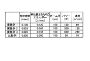
精密加工CO2レーザ(商品名SILAS−SAM(SPL2305型);澁谷工業製、波長10.6μm)を使用して、前記光学フィルムの表面保護フィルム側からレーザを照射して切断した。このとき、実施例1では、図2に示すよにう、単位長さ当たりのエネルギを0.120J/mmに設定し且つ連続照射時間を0.100msecに設定した。また、レーザビームのビーム径は100μmに調整し、パワーは120Wに調整した。更に、レーザビームのスキャン速度は、60m/minに設定した。
(Cutting method)
Using a precision-processed CO 2 laser (trade name SILAS-SAM (SPL2305 type); manufactured by Kasuya Kogyo Co., Ltd., wavelength 10.6 μm), the optical film was cut by irradiating the laser from the surface protective film side. At this time, in Example 1, as shown in FIG. 2, the energy per unit length was set to 0.120 J / mm, and the continuous irradiation time was set to 0.100 msec. Further, the beam diameter of the laser beam was adjusted to 100 μm, and the power was adjusted to 120 W. Further, the scanning speed of the laser beam was set to 60 m / min.
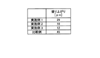
前記実施例1に従って光学フィルムを切断した際に、フィルム切断面に発生した盛り上がり部を測定した結果が図3に示されている。 FIG. 3 shows the result of measuring the raised portion generated on the film cut surface when the optical film was cut according to Example 1.
実施例2では、図2に示すように、単位長さ当たりのエネルギを0.167J/mmに設定し且つ連続照射時間を0.033msecに設定した。また、レーザビームのビーム径は100μmに調整し、パワーは500Wに調整した。更に、レーザビームのスキャン速度は、180m/minに設定した。これら以外の条件については、前記実施例1の場合と同一条件で行った。 In Example 2, as shown in FIG. 2, the energy per unit length was set to 0.167 J / mm, and the continuous irradiation time was set to 0.033 msec. Further, the beam diameter of the laser beam was adjusted to 100 μm, and the power was adjusted to 500 W. Further, the scanning speed of the laser beam was set to 180 m / min. About conditions other than these, it carried out on the same conditions as the case of the said Example 1. FIG.
前記実施例2に従って光学フィルムを切断した際に、フィルム切断面に発生した盛り上がり部を測定した結果が図3に示されている。 FIG. 3 shows the result of measuring the raised portion generated on the film cut surface when the optical film was cut according to Example 2.
実施例3では、図2に示すように、単位長さ当たりのエネルギを0.155J/mmに設定し且つ連続照射時間を0.025msecに設定した。また、レーザビームのビーム径は100μmに調整し、パワーは620Wに調整した。更に、レーザビームのスキャン速度は、240m/minに設定した。これら以外の条件については、前記実施例1の場合と同一条件で行った。 In Example 3, as shown in FIG. 2, the energy per unit length was set to 0.155 J / mm, and the continuous irradiation time was set to 0.025 msec. Further, the beam diameter of the laser beam was adjusted to 100 μm, and the power was adjusted to 620 W. Further, the scanning speed of the laser beam was set to 240 m / min. About conditions other than these, it carried out on the same conditions as the case of the said Example 1. FIG.
前記実施例3に従って光学フィルムを切断した際に、フィルム切断面に発生した盛り上がり部を測定した結果が図3に示されている。 FIG. 3 shows the result of measuring the raised portion generated on the film cut surface when the optical film was cut according to Example 3.
(比較例)
比較例では、図2に示すように、単位長さ当たりのエネルギを0.300J/mmに設定し且つ連続照射時間を0.600msecに設定した。また、レーザビームのビーム径は100μmに調整し、パワーは50Wに調整した。更に、レーザビームのスキャン速度は、10m/minに設定した。これら以外の条件については、前記実施例1の場合と同一条件で行った。
(Comparative example)
In the comparative example, as shown in FIG. 2, the energy per unit length was set to 0.300 J / mm and the continuous irradiation time was set to 0.600 msec. Further, the beam diameter of the laser beam was adjusted to 100 μm, and the power was adjusted to 50 W. Further, the scanning speed of the laser beam was set to 10 m / min. About conditions other than these, it carried out on the same conditions as the case of the said Example 1. FIG.
前記比較例に従って光学フィルムを切断した際に、フィルム切断面に発生した盛り上がり部を測定した結果が図3に示されている。 FIG. 3 shows the result of measuring the raised portion generated on the film cut surface when the optical film was cut according to the comparative example.
図3において、実施例1に従って切断された光学フィルムの切断面に発生した盛り上がり部のサイズは29μmであり、実施例2に従って切断された光学フィルムの切断面に発生した盛り上がり部のサイズは18μmであり、また、実施例3に従って切断された光学フィルムの切断面に発生した盛り上がり部のサイズは12μmであった。これより、いずれの実施例においても、盛り上がり部のサイズを30μm以下に抑制することができる。
このように、単位長さ当たりのエネルギが0.12〜0.167J/mmであり且つ連続照射時間が0.1msec以下の条件で、レーザビームを光学フィルム1に照射して光学フィルムを切断することにより、光学フィルムの切断面に発生する盛り上がり部のサイズを30μm以下に抑制可能なことが分かる。
In FIG. 3, the size of the raised portion generated on the cut surface of the optical film cut according to Example 1 is 29 μm, and the size of the raised portion generated on the cut surface of the optical film cut according to Example 2 is 18 μm. In addition, the size of the raised portion generated on the cut surface of the optical film cut according to Example 3 was 12 μm. Thus, in any of the embodiments, the size of the raised portion can be suppressed to 30 μm or less.
As described above, the optical film 1 is cut by irradiating the optical film 1 with the laser beam under the condition that the energy per unit length is 0.12 to 0.167 J / mm and the continuous irradiation time is 0.1 msec or less. This shows that the size of the raised portion generated on the cut surface of the optical film can be suppressed to 30 μm or less.
これに対して、比較例では、単位長さ当たりのエネルギが0.12〜0.167J/mmを外れた0.300J/mmであり、且つ、連続照射時間も0.1msecを越えた0.600m/secであることから、比較例に従って切断された光学フィルムの切断面に発生した盛り上がり部のサイズは45μmと大きくなってしまうことが分かる。 On the other hand, in the comparative example, the energy per unit length is 0.300 J / mm, which deviates from 0.12 to 0.167 J / mm, and the continuous irradiation time exceeds 0.1 msec. Since it is 600 m / sec, it turns out that the size of the rising part which generate | occur | produced on the cut surface of the optical film cut | disconnected according to the comparative example will become large with 45 micrometers.
本発明に係る光学フィルムの切断方法によれば、レーザビームがガウシアンビームの特性を有する場合であっても、レーザビームが照射される単位長さ当たりのエネルギ及び連続照射時間を制御したレーザビームを使用して偏光フィルム等の光学フィルムを切断することにより、光学フィルムの切断面における盛り上がりサイズを可及的に小さくすることが可能であり、もって各種の光学パネルに組み込んだ際に接着不良や光学的不具合が発生することを防止可能な光学フィルムの切断方法及びその切断方法により切断された光学フィルムを提供することができる。 According to the optical film cutting method of the present invention, even when the laser beam has the characteristics of a Gaussian beam, the laser beam with the energy per unit length irradiated with the laser beam and the continuous irradiation time is controlled. By cutting the optical film such as polarizing film, it is possible to reduce the rising size of the cut surface of the optical film as much as possible. It is possible to provide an optical film cutting method and an optical film cut by the cutting method capable of preventing the occurrence of mechanical trouble.
1 光学フィルム
2 偏光板
3 表面保護フィルム
4 粘着剤層
5 セパレータ
DESCRIPTION OF SYMBOLS 1
Claims (3)
Priority Applications (7)
| Application Number | Priority Date | Filing Date | Title |
|---|---|---|---|
| JP2006226870A JP4808106B2 (en) | 2006-08-23 | 2006-08-23 | Cutting method of optical film |
| KR1020097003599A KR101249080B1 (en) | 2006-08-23 | 2007-08-20 | Optical film cutting method and optical film |
| US12/438,234 US20100116800A1 (en) | 2006-08-23 | 2007-08-20 | Optical film cutting method and optical film |
| EP07792747.3A EP2055423B1 (en) | 2006-08-23 | 2007-08-20 | A method of cutting an optical film by using a laser beam |
| PCT/JP2007/066134 WO2008023672A1 (en) | 2006-08-23 | 2007-08-20 | Optical film cutting method and optical film |
| CN2007800309066A CN101505909B (en) | 2006-08-23 | 2007-08-20 | Optical film cutting method and optical film |
| TW096131164A TWI402129B (en) | 2006-08-23 | 2007-08-23 | Optical film cutting method and optical film |
Applications Claiming Priority (1)
| Application Number | Priority Date | Filing Date | Title |
|---|---|---|---|
| JP2006226870A JP4808106B2 (en) | 2006-08-23 | 2006-08-23 | Cutting method of optical film |
Publications (2)
| Publication Number | Publication Date |
|---|---|
| JP2008051964A true JP2008051964A (en) | 2008-03-06 |
| JP4808106B2 JP4808106B2 (en) | 2011-11-02 |
Family
ID=39106757
Family Applications (1)
| Application Number | Title | Priority Date | Filing Date |
|---|---|---|---|
| JP2006226870A Active JP4808106B2 (en) | 2006-08-23 | 2006-08-23 | Cutting method of optical film |
Country Status (7)
| Country | Link |
|---|---|
| US (1) | US20100116800A1 (en) |
| EP (1) | EP2055423B1 (en) |
| JP (1) | JP4808106B2 (en) |
| KR (1) | KR101249080B1 (en) |
| CN (1) | CN101505909B (en) |
| TW (1) | TWI402129B (en) |
| WO (1) | WO2008023672A1 (en) |
Cited By (4)
| Publication number | Priority date | Publication date | Assignee | Title |
|---|---|---|---|---|
| JP2010072414A (en) * | 2008-09-19 | 2010-04-02 | Konica Minolta Opto Inc | Optical film, method for manufacturing optical film, and polarizing plate |
| JP2017207585A (en) * | 2016-05-17 | 2017-11-24 | 日東電工株式会社 | Optical laminate and method of manufacturing optical film piece using optical laminate |
| WO2018062031A1 (en) * | 2016-09-30 | 2018-04-05 | 住友化学株式会社 | Optical film and method for manufacturing same |
| JP2021144208A (en) * | 2020-03-10 | 2021-09-24 | 住友化学株式会社 | Laminated sheet and manufacturing method therefor |
Families Citing this family (15)
| Publication number | Priority date | Publication date | Assignee | Title |
|---|---|---|---|---|
| JP2008073742A (en) * | 2006-09-22 | 2008-04-03 | Nitto Denko Corp | Optical film cutting method and optical film |
| JP5553397B2 (en) * | 2007-07-19 | 2014-07-16 | 日東電工株式会社 | Laser processing method |
| EP2537633B1 (en) * | 2011-06-24 | 2014-05-07 | Comadur S.A. | Bevel machining system |
| KR101477453B1 (en) * | 2011-11-21 | 2014-12-29 | 수미토모 케미칼 컴퍼니 리미티드 | Optical member laminate manufacturing system, manufacturing method, and recording medium |
| CN104583847B (en) * | 2012-09-07 | 2018-04-13 | 住友化学株式会社 | Manufacturing equipment of optical member bonding body |
| KR101451530B1 (en) * | 2013-12-26 | 2014-10-16 | 김충덕 | Manufacturing apparatus for polarized lens film and manufacturing method thereof |
| CN103962730B (en) | 2014-04-29 | 2017-01-18 | 京东方科技集团股份有限公司 | Cutting method and device for flexible display panel and control device |
| KR101817388B1 (en) * | 2014-09-30 | 2018-01-10 | 주식회사 엘지화학 | Cutting method for the polarizing plate, polarizing plate cut usuing the same |
| CN107003459B (en) * | 2014-11-05 | 2019-04-05 | 住友化学株式会社 | Manufacturing method of polarizing plate monolith |
| KR101858432B1 (en) * | 2016-03-23 | 2018-05-16 | 동우 화인켐 주식회사 | Window substrate and preparing method thereof |
| JP6754621B2 (en) * | 2016-06-10 | 2020-09-16 | 日東電工株式会社 | How to cut out the film |
| JP2019093449A (en) * | 2017-11-27 | 2019-06-20 | 日東電工株式会社 | Laser processing method of plastic film, and plastic film |
| CN108145320A (en) * | 2017-12-29 | 2018-06-12 | 南京联信自动化科技有限公司 | A kind of cutting method of decorative adhesive film of digital product |
| KR102769664B1 (en) * | 2018-08-20 | 2025-02-17 | 니폰 제온 가부시키가이샤 | Method for manufacturing cut film, cut film, and film for cut film |
| CN109397673A (en) * | 2018-10-31 | 2019-03-01 | 江苏赛诺格兰医疗科技有限公司 | A kind of ESR film method for folding |
Citations (1)
| Publication number | Priority date | Publication date | Assignee | Title |
|---|---|---|---|---|
| JPS6434593A (en) * | 1987-07-31 | 1989-02-06 | Teijin Ltd | Method for cutting and processing film |
Family Cites Families (13)
| Publication number | Priority date | Publication date | Assignee | Title |
|---|---|---|---|---|
| JPS60121090A (en) * | 1983-12-02 | 1985-06-28 | Toray Ind Inc | Cutting method of film |
| JPH0491879A (en) * | 1990-08-08 | 1992-03-25 | Teijin Ltd | Method for cutting film |
| US5444035A (en) * | 1990-08-17 | 1995-08-22 | Minnesota Mining And Manufacturing Company | Laser perforation of paper |
| WO1994029069A1 (en) * | 1993-06-04 | 1994-12-22 | Seiko Epson Corporation | Apparatus and method for laser machining, and liquid crystal panel |
| JPH0722552A (en) * | 1993-07-02 | 1995-01-24 | Daido Steel Co Ltd | Molding method for IC lead frame |
| JPH1177352A (en) * | 1997-08-29 | 1999-03-23 | Amada Co Ltd | High speed taperless cutting method in laser beam machining |
| CN100410196C (en) * | 2001-11-08 | 2008-08-13 | 夏普株式会社 | Method and apparatus for cutting glass substrate, liquid crystal panel, and apparatus for manufacturing liquid crystal panel |
| JPWO2003040049A1 (en) * | 2001-11-08 | 2005-03-03 | シャープ株式会社 | Glass substrate cutting method, glass substrate cutting device, liquid crystal panel, and liquid crystal panel manufacturing apparatus |
| US7007710B2 (en) * | 2003-04-21 | 2006-03-07 | Predicant Biosciences, Inc. | Microfluidic devices and methods |
| US7344671B2 (en) * | 2003-11-26 | 2008-03-18 | Glopak Inc. | Optical sealing clamp and a method for sealing and cutting polymeric sheets with a laser |
| JP4233999B2 (en) | 2003-12-25 | 2009-03-04 | 日東電工株式会社 | Laminated polarizing plate and manufacturing method thereof |
| JP2006061926A (en) | 2004-08-25 | 2006-03-09 | Shoei Insatsu Kk | Cutting method by laser beam, laser beam cutting device used for the method, and article manufactured by the method |
| JP4156602B2 (en) | 2005-02-18 | 2008-09-24 | 株式会社日立ハイテクサイエンスシステムズ | Non-radiation electron capture detector |
-
2006
- 2006-08-23 JP JP2006226870A patent/JP4808106B2/en active Active
-
2007
- 2007-08-20 US US12/438,234 patent/US20100116800A1/en not_active Abandoned
- 2007-08-20 KR KR1020097003599A patent/KR101249080B1/en active Active
- 2007-08-20 EP EP07792747.3A patent/EP2055423B1/en not_active Ceased
- 2007-08-20 CN CN2007800309066A patent/CN101505909B/en active Active
- 2007-08-20 WO PCT/JP2007/066134 patent/WO2008023672A1/en not_active Ceased
- 2007-08-23 TW TW096131164A patent/TWI402129B/en active
Patent Citations (1)
| Publication number | Priority date | Publication date | Assignee | Title |
|---|---|---|---|---|
| JPS6434593A (en) * | 1987-07-31 | 1989-02-06 | Teijin Ltd | Method for cutting and processing film |
Cited By (6)
| Publication number | Priority date | Publication date | Assignee | Title |
|---|---|---|---|---|
| JP2010072414A (en) * | 2008-09-19 | 2010-04-02 | Konica Minolta Opto Inc | Optical film, method for manufacturing optical film, and polarizing plate |
| JP2017207585A (en) * | 2016-05-17 | 2017-11-24 | 日東電工株式会社 | Optical laminate and method of manufacturing optical film piece using optical laminate |
| WO2018062031A1 (en) * | 2016-09-30 | 2018-04-05 | 住友化学株式会社 | Optical film and method for manufacturing same |
| JP2018059070A (en) * | 2016-09-30 | 2018-04-12 | 住友化学株式会社 | Optical film and production method of the same |
| JP7021887B2 (en) | 2016-09-30 | 2022-02-17 | 住友化学株式会社 | Optical film manufacturing method |
| JP2021144208A (en) * | 2020-03-10 | 2021-09-24 | 住友化学株式会社 | Laminated sheet and manufacturing method therefor |
Also Published As
| Publication number | Publication date |
|---|---|
| WO2008023672A1 (en) | 2008-02-28 |
| EP2055423B1 (en) | 2013-05-22 |
| CN101505909B (en) | 2013-09-11 |
| EP2055423A1 (en) | 2009-05-06 |
| KR101249080B1 (en) | 2013-03-29 |
| TW200810868A (en) | 2008-03-01 |
| TWI402129B (en) | 2013-07-21 |
| JP4808106B2 (en) | 2011-11-02 |
| CN101505909A (en) | 2009-08-12 |
| US20100116800A1 (en) | 2010-05-13 |
| EP2055423A4 (en) | 2010-11-24 |
| KR20090103991A (en) | 2009-10-05 |
Similar Documents
| Publication | Publication Date | Title |
|---|---|---|
| TWI402129B (en) | Optical film cutting method and optical film | |
| TWI387501B (en) | Optical film cutting method and optical film | |
| JP5429777B2 (en) | Polarizer | |
| CN206920638U (en) | Polarization plates and image display device | |
| JP5930636B2 (en) | Polarizer | |
| KR102314053B1 (en) | Polarizing plate, polarizing plate with adhesive and liquid crystal display device | |
| TWI422878B (en) | Polarizing plate and its manufacturing method | |
| TWI485065B (en) | Polarizing plate and its manufacturing method | |
| JP2008197310A (en) | Thin polarizing plate, composite polarizing plate, image display device, and manufacturing method of composite polarizing plate | |
| US20050153079A1 (en) | Method of manufacturing laminated polarizing plate, laminated polarizing plate obtained by the method, and image display including the same | |
| JP2015072454A (en) | Manufacturing method of end-face processed polarizing plate | |
| KR102473609B1 (en) | Method for manufacturing laminated polarizing plate and method for manufacturing polarizing plate | |
| JP5951870B1 (en) | Manufacturing method of polarizing plate | |
| JP2006062240A (en) | Manufacturing method of non-glare reflection-preventive film and non-glare reflection-preventive film | |
| US12360303B2 (en) | Polarizing plate and optical display apparatus comprising same | |
| KR102294328B1 (en) | Optical film and polarizing plate | |
| JP6181804B2 (en) | Polarizer | |
| JP2010197681A (en) | Method of manufacturing polarizing plate with adhesive | |
| WO2020213494A1 (en) | Optical laminate, and image display device | |
| CN112969940A (en) | Polarizing plate | |
| KR20220064654A (en) | Polarizing Plate and Display Device Comprising the Same |
Legal Events
| Date | Code | Title | Description |
|---|---|---|---|
| A621 | Written request for application examination |
Free format text: JAPANESE INTERMEDIATE CODE: A621 Effective date: 20081110 |
|
| A131 | Notification of reasons for refusal |
Free format text: JAPANESE INTERMEDIATE CODE: A131 Effective date: 20110426 |
|
| A521 | Request for written amendment filed |
Free format text: JAPANESE INTERMEDIATE CODE: A523 Effective date: 20110623 |
|
| TRDD | Decision of grant or rejection written | ||
| A01 | Written decision to grant a patent or to grant a registration (utility model) |
Free format text: JAPANESE INTERMEDIATE CODE: A01 Effective date: 20110816 |
|
| A01 | Written decision to grant a patent or to grant a registration (utility model) |
Free format text: JAPANESE INTERMEDIATE CODE: A01 |
|
| A61 | First payment of annual fees (during grant procedure) |
Free format text: JAPANESE INTERMEDIATE CODE: A61 Effective date: 20110816 |
|
| FPAY | Renewal fee payment (event date is renewal date of database) |
Free format text: PAYMENT UNTIL: 20140826 Year of fee payment: 3 |
|
| R150 | Certificate of patent or registration of utility model |
Ref document number: 4808106 Country of ref document: JP Free format text: JAPANESE INTERMEDIATE CODE: R150 |
|
| R250 | Receipt of annual fees |
Free format text: JAPANESE INTERMEDIATE CODE: R250 |
|
| R250 | Receipt of annual fees |
Free format text: JAPANESE INTERMEDIATE CODE: R250 |
|
| R250 | Receipt of annual fees |
Free format text: JAPANESE INTERMEDIATE CODE: R250 |
|
| R250 | Receipt of annual fees |
Free format text: JAPANESE INTERMEDIATE CODE: R250 |
|
| R250 | Receipt of annual fees |
Free format text: JAPANESE INTERMEDIATE CODE: R250 |
|
| R250 | Receipt of annual fees |
Free format text: JAPANESE INTERMEDIATE CODE: R250 |
|
| R250 | Receipt of annual fees |
Free format text: JAPANESE INTERMEDIATE CODE: R250 |
|
| R250 | Receipt of annual fees |
Free format text: JAPANESE INTERMEDIATE CODE: R250 |
|
| R250 | Receipt of annual fees |
Free format text: JAPANESE INTERMEDIATE CODE: R250 |
|
| R250 | Receipt of annual fees |
Free format text: JAPANESE INTERMEDIATE CODE: R250 |
|
| R250 | Receipt of annual fees |
Free format text: JAPANESE INTERMEDIATE CODE: R250 |
|
| R250 | Receipt of annual fees |
Free format text: JAPANESE INTERMEDIATE CODE: R250 |