JP2008021040A - Bus master circuit, bus control method and computer program - Google Patents
Bus master circuit, bus control method and computer program Download PDFInfo
- Publication number
- JP2008021040A JP2008021040A JP2006190907A JP2006190907A JP2008021040A JP 2008021040 A JP2008021040 A JP 2008021040A JP 2006190907 A JP2006190907 A JP 2006190907A JP 2006190907 A JP2006190907 A JP 2006190907A JP 2008021040 A JP2008021040 A JP 2008021040A
- Authority
- JP
- Japan
- Prior art keywords
- bus
- hardware
- signal
- state
- register
- Prior art date
- Legal status (The legal status is an assumption and is not a legal conclusion. Google has not performed a legal analysis and makes no representation as to the accuracy of the status listed.)
- Pending
Links
Images


Landscapes
- Bus Control (AREA)
Abstract
Description
本発明は、バスマスタ回路、バス制御方法、及びコンピュータプログラムに関し、特に、バスに接続されたハードウェアの状態を検出するために用いて好適なものである。 The present invention relates to a bus master circuit, a bus control method, and a computer program, and is particularly suitable for use in detecting the state of hardware connected to a bus.
一般にプロセッサと1つ以上のハードウェアとが接続されたバスを備えたシステムLSIでは、ハードウェアを制御するために、プロセッサがハードウェアの状態を把握し、そのハードウェアの状態に応じてそのハードウェア又はその他のハードウェアを制御する。
プロセッサがハードウェアの状態を把握する手法として、ハードウェアの内部状態を示すレジスタをハードウェアの内部に設け、プロセッサがレジスタを継続的に監視することによってハードウェアの内部状態を知るポーリング手法がある。尚、以下の説明では、レジスタを監視することをポーリングと称する。また、ハードウェアの内部でレジスタの状態が予め決められた状態になったときに、ハードウェアがプロセッサに割り込み信号を通知する割り込み通知手法も用いられている。特許文献1には、通信周期内の任意のクロック数で割り込み信号を発生させるレジスタの設定値と、サイクルタイマ回路の設定値とを比較器で比較し、比較器が出力する指令を受け取ると割り込み信号をCPUに出力する割り込み発生回路が記載されている。この割り込み発生回路では、ノイズ等が発生してもホストCPUに与える割り込み信号が発生するようにしている。
In general, in a system LSI having a bus to which a processor and one or more hardware are connected, in order to control the hardware, the processor grasps the state of the hardware, and the hardware according to the state of the hardware. Hardware or other hardware.
As a method for the processor to grasp the hardware state, there is a polling method in which a register indicating the internal state of the hardware is provided in the hardware, and the processor continuously monitors the register to know the internal state of the hardware. . In the following description, monitoring a register is referred to as polling. An interrupt notification method is also used in which the hardware notifies the processor of an interrupt signal when the register state in the hardware reaches a predetermined state. In
プロセッサは、前述したどちらかの手法を用いてハードウェアの内部状態を検出し、そのハードウェアの内部状態に応じてハードウェアを制御していた。
ハードウェアの内部状態を示すレジスタをプロセッサがポーリングする手法では、レジスタをリードするコマンドをプロセッサが継続的に何度も発行するため、プロセッサに多大な負荷がかかる。従って、割り込み通知手法が一般的に使われる。
The processor detects the internal state of the hardware using one of the methods described above, and controls the hardware according to the internal state of the hardware.
In the method in which the processor polls a register indicating the internal state of the hardware, the processor continuously issues a command to read the register many times, and thus a heavy load is applied to the processor. Therefore, the interrupt notification method is generally used.
しかしながら、あらゆる状況において割り込み通知手法を使用できるわけではない。例えば、ハードウェアの内部状態が設計段階では想定していなかった状態になったために、ハードウェアが割り込み信号をプロセッサに通知できない場合、プロセッサは、ポーリングを行ってハードウェアの内部状態を検出し、ハードウェアを制御する必要がある。また、バグ等によりハードウェアが意図した割り込み処理を行えない場合も同様に、プロセッサがポーリングを行ってハードウェアを制御する必要がある。
このような不都合を解消するために、バックアップ用のサブプロセッサを設け、サブプロセッサがポーリングを行ってハードウェアの内部状態を検出し、検出したハードウェアの内部状態をメインプロセッサに通知してハードウェアを制御する手法も採られてきた。
However, the interrupt notification technique cannot be used in all situations. For example, if the hardware cannot notify the processor of an interrupt signal because the hardware internal state has not been assumed at the design stage, the processor performs polling to detect the hardware internal state, You need to control the hardware. Similarly, when the hardware cannot perform the interrupt processing intended by the hardware due to a bug or the like, the processor needs to perform polling to control the hardware.
In order to solve such inconvenience, a sub processor for backup is provided, and the sub processor performs polling to detect the internal state of the hardware, and notifies the main processor of the detected internal state of the hardware. A method for controlling the above has also been adopted.
しかしながら、前述したサブプロセッサを用いてハードウェアの内部状態を検出する手法では、次のような不都合があった。
まず、サブプロセッサは、リセットが解除された後に、実行するプログラムのコードをROM等から読み出すブート処理が必要になる。従って、システムの起動に時間がかかる上に、プログラムを格納するためのメモリ領域が必要となる。
However, the method for detecting the internal state of the hardware using the sub-processor described above has the following disadvantages.
First, after the reset is released, the sub processor needs a boot process for reading the code of the program to be executed from the ROM or the like. Therefore, it takes time to start the system, and a memory area for storing the program is required.
また、メインプロセッサとサブプロセッサとの通信(マルチプロセッサ間通信)が必要となる。従って、双方のプロセッサが使用できる共有メモリを確保しなければならない。共有メモリには、サブプロセッサからメインプロセッサへの処理依頼メッセージを格納する領域と、その処理依頼に対するメインプロセッサからサブプロセッサへの応答メッセージを格納する領域とが必要になる。更に共有メモリには、メインプロセッサからサブプロセッサへの処理依頼メッセージを格納する領域と、その処理依頼に対するサブプロセッサからメインプロセッサへの応答メッセージを格納する領域も必要になる。 Further, communication (inter-multiprocessor communication) between the main processor and the sub processor is required. Therefore, a shared memory that can be used by both processors must be secured. The shared memory requires an area for storing a processing request message from the sub processor to the main processor and an area for storing a response message from the main processor to the sub processor in response to the processing request. Further, the shared memory also requires an area for storing a processing request message from the main processor to the sub processor and an area for storing a response message from the sub processor to the main processor in response to the processing request.
サブプロセッサからメインプロセッサへの処理依頼をする場合、サブプロセッサは、メインプロセッサへの処理依頼メッセージ格納領域(共有メモリ)に、メインプロセッサへの処理依頼メッセージを書き込んで、メインプロセッサに対して割り込み通知を行う。通常プロセッサはスレーブインターフェースを備えない。従って、この割り込み通知をクリアする場合、メインプロセッサは、サブプロセッサへの処理依頼メッセージ格納領域(共有メモリ)に、サブプロセッサへの処理依頼メッセージを書き込んで、サブプロセッサに対して割り込み通知を行う。このような割り込みクリアのシーケンスは、割り込みクリアレジスタをクリアして行う通常の処理に比べると処理時間がかかる。 When making a processing request from the sub processor to the main processor, the sub processor writes the processing request message to the main processor in the processing request message storage area (shared memory) to the main processor, and notifies the main processor of an interrupt. I do. Usually the processor does not have a slave interface. Therefore, when clearing this interrupt notification, the main processor writes the processing request message for the sub processor in the processing request message storage area (shared memory) for the sub processor, and notifies the sub processor of the interrupt. Such an interrupt clear sequence takes more processing time than normal processing performed by clearing the interrupt clear register.
また、コストを削減するシステムLSIにおいては、例えば面積の小さな8ビットマイコンであっても、サブプロセッサを設けたことによるシステムLSIの面積の増加は好ましくない。更に、サブプロセッサを設けると、サブプロセッサ本体に加えて、サブプロセッサがプログラムを実行するためのワークメモリ領域等のハードウェアリソースが必要になる。このようなハードウェアリソースは、システムLSIの面積が増加する要因となる。 Further, in the system LSI for reducing the cost, for example, even if the area is an 8-bit microcomputer, an increase in the area of the system LSI due to the provision of the sub processor is not preferable. Further, when the sub processor is provided, in addition to the sub processor main body, hardware resources such as a work memory area for the sub processor to execute the program are required. Such hardware resources become a factor that increases the area of the system LSI.
本発明はこのような問題点に鑑み、バスに接続されたハードウェアの状態を検出する際の処理速度を向上させると共に、システムの面積の増加を抑えるようにすることを目的とする。 The present invention has been made in view of such problems, and it is an object of the present invention to improve the processing speed when detecting the state of hardware connected to a bus and suppress an increase in the area of the system.
本発明のバスマスタ回路は、プロセッサ及び1つ以上のハードウェアとバスを介して相互に接続されたバスマスタ回路であって、前記バスにバスマスタとしてアクセスして、前記バスを介して相互に接続されたハードウェアの状態を検出する検出手段と、前記検出手段により検出されたハードウェアの状態を判別する判別手段と、前記判別手段により判別されたハードウェアの状態に基づいて制御信号を生成する生成手段と、前記生成手段により生成された制御信号を前記バスに出力する出力手段とを有することを特徴とする。 The bus master circuit of the present invention is a bus master circuit that is mutually connected via a bus with a processor and one or more hardware, and is connected to each other via the bus by accessing the bus as a bus master. Detection means for detecting a hardware state, determination means for determining the hardware state detected by the detection means, and generation means for generating a control signal based on the hardware state determined by the determination means And output means for outputting the control signal generated by the generating means to the bus.
本発明のバス制御方法は、バスにバスマスタとしてアクセスして、前記バスを介して相互に接続されたハードウェアの状態を検出する検出ステップと、前記検出ステップにより検出されたハードウェアの状態を判別する判別ステップと、前記判別ステップにより判別されたハードウェアの状態に基づいて制御信号を生成する生成ステップと、前記生成ステップにより生成された制御信号を前記バスに出力する出力ステップとを有することを特徴とする。 The bus control method according to the present invention includes a detection step of accessing a bus as a bus master and detecting a state of hardware connected to each other via the bus, and determining a hardware state detected by the detection step. And a generating step for generating a control signal based on a hardware state determined by the determining step, and an output step for outputting the control signal generated by the generating step to the bus. Features.
本発明のコンピュータプログラムは、バスにバスマスタとしてアクセスして、前記バスを介して相互に接続されたハードウェアの状態を検出する検出ステップと、前記検出ステップにより検出されたハードウェアの状態を判別する判別ステップと、前記判別ステップにより判別されたハードウェアの状態に基づいて制御信号を生成する生成ステップと、前記生成ステップにより生成された制御信号を前記バスに出力する出力ステップとをコンピュータに実行させることを特徴とする。 A computer program according to the present invention accesses a bus as a bus master, detects a state of hardware connected to each other via the bus, and determines a hardware state detected by the detection step Causing the computer to execute a determination step, a generation step for generating a control signal based on the hardware state determined in the determination step, and an output step for outputting the control signal generated in the generation step to the bus It is characterized by that.
本発明によれば、バスにバスマスタとしてアクセスして、ハードウェアの状態を検出し、検出したハードウェアの状態に基づいて制御信号を生成して出力するようにした。従って、プロセッサがハードウェアの状態を検出する必要がなくなるので、プロセッサの負荷を削減することと、ハードウェアの状態を検出する際の動作速度を向上させることと、システムの面積の増加を抑えることとを実現することが可能になる。 According to the present invention, the bus is accessed as a bus master, the hardware state is detected, and the control signal is generated and output based on the detected hardware state. This eliminates the need for the processor to detect the hardware status, thus reducing the load on the processor, improving the operating speed when detecting the hardware status, and suppressing an increase in system area. Can be realized.
また、本発明の他の特徴によれば、ハードウェアの状態に基づいて、そのハードウェアと異なる第2のハードウェアの動作に関わる制御信号を生成し、生成した制御信号を、バスを介して第2のハードウェアに出力するようにした。従って、プロセッサへの割り込み処理を行わずにハードウェアモジュールの動作を制御することが可能になる。 According to another aspect of the invention, based on the state of the hardware, a control signal related to the operation of the second hardware different from the hardware is generated, and the generated control signal is transmitted via the bus. Output to the second hardware. Therefore, it is possible to control the operation of the hardware module without performing interrupt processing to the processor.
また、本発明のその他の特徴によれば、ハードウェアの状態に基づいて、プロセッサへ供給されるクロックを制御するための制御信号を生成するようにした。従って、例えば、プロセッサが停止している状況においても、ハードウェアの動作を制御することが可能になる。 According to another feature of the present invention, a control signal for controlling a clock supplied to the processor is generated based on a hardware state. Therefore, for example, even when the processor is stopped, the hardware operation can be controlled.
また、本発明のその他の特徴によれば、ハードウェアの状態を検出する間隔をあけるようにしたので、バスの負荷を軽減することが可能になる。
更に、本発明のその他の特徴によれば、ハードウェアの状態を検出する間隔をプログラマブルに設定可能にしたので、ハードウェアの状態の検出頻度を調整することが可能になる。
In addition, according to another feature of the present invention, the interval for detecting the hardware state is provided, so that the load on the bus can be reduced.
Furthermore, according to the other feature of the present invention, since the interval for detecting the hardware state can be set in a programmable manner, the detection frequency of the hardware state can be adjusted.
また、本発明のその他の特徴によれば、制御信号の出力先のアドレスと、制御信号に含めるデータとをプログラマブルに設定可能にしたので、様々なハードウェアを様々な形態で制御することが可能になる。 In addition, according to another feature of the present invention, the output destination address of the control signal and the data included in the control signal can be set in a programmable manner, so that various hardware can be controlled in various forms. become.
また、本発明のその他の特徴によれば、状態を検出するハードウェアのアドレスをプログラマブルに設定可能にしたので、様々なハードウェアの状態を検出することが可能になる。
また、本発明のその他の特徴によれば、ハードウェアの状態を判別するための条件をプログラマブルに設定可能にしたので、様々な条件でハードウェアの状態を判別することが可能になる。
According to another feature of the present invention, the hardware address for detecting the state can be set in a programmable manner, so that various hardware states can be detected.
According to another feature of the present invention, the condition for determining the hardware state can be set in a programmable manner, so that the hardware state can be determined under various conditions.
(第1の実施形態)
以下に、図面を参照しながら、本発明の第1の実施形態について説明する。
まず、本実施形態のバスマスタ回路の基本構成を説明する。図1は、バスマスタ回路の基本構成の一例を示す図である。
図1において、バスマスタ回路101は、バスマスタ機能ブロック102、状態検出ブロック103、条件判定ブロック104、ハードウェア制御ブロック105、制御レジスタ群106、及びバススレーブ機能ブロック107を有する。
(First embodiment)
Hereinafter, a first embodiment of the present invention will be described with reference to the drawings.
First, the basic configuration of the bus master circuit of this embodiment will be described. FIG. 1 is a diagram illustrating an example of a basic configuration of a bus master circuit.
In FIG. 1, the
バスマスタ機能ブロック102は、システムバス108のバスプロトコルに従って、バスマスタとしてシステムバス108にアクセス(バスアクセス)するためのマスタインターフェースのブロックである。
状態検出ブロック103は、システムバス108に接続されたハードウェアの内部状態を表示するレジスタの設定を読み出すことを、バスマスタ機能ブロック102に継続的に要求する。以下の説明では、この要求を必要に応じてリード要求と称する。また、システムバス108に接続されたハードウェアの内部状態を表示するレジスタの設定を、必要に応じてリードデータと称する。そして、状態検出ブロック103は、リード要求に基づいてバスマスタ機能ブロック102が取得したリードデータを受け取る。また、状態検出ブロック103は、システムバス108に接続されたハードウェアの内部状態を表示するレジスタのアドレスや、ポーリングを行う間隔等、バスマスタ回路101が行うポーリングを制御する。
The bus
The state detection block 103 continuously requests the bus
条件判定ブロック104は、状態検出ブロック103からリードデータを受け取り、受け取ったリードデータと判定条件とを比較して、条件を満たしているか否かを判定するブロックである。そして、条件判定ブロック104は、判定した条件を満たしているか否かを示す条件判定フラグを生成する。
ハードウェア制御ブロック105は、条件判定ブロック104から条件判定フラグを受け取り、受け取った条件判定フラグに基づき、システムバス108に接続されたプロセッサやハードウェアを制御するための制御信号を生成するブロックである。
The
The
制御レジスタ群106は、バスマスタ回路101の動作設定を行うレジスタ群である。このレジスタ群は、例えば、システムバス108に接続されたCPU等によってプログラマブルに設定される。
バススレーブ機能ブロック107は、システムバス108に接続されたCPU等が制御レジスタ群106にアクセスするためのインターフェースである。このバススレーブ機能ブロック107は、システムバス108のバスプロトコルに従って、バススレーブとしてシステムバス108とアクセス(バスアクセス)するためのスレーブインターフェースのブロックである。
The control register group 106 is a register group for setting the operation of the
The bus
次に、システムバス108に接続されたハードウェアの内部状態を表示するレジスタを、バスマスタ回路101を用いてポーリングし、ポーリングした結果に基づいて、プロセッサやハードウェアを制御する手法の具体例を詳細に述べる。ここでは、バスマスタ回路101の要件の一つであるハードウェア制御ブロック105を、システムバス108に接続されたCPUに対する割り込み信号を生成する機能を有する割り込み信号生成ブロックで構成する場合を例に挙げて説明する。
Next, a specific example of a method of polling a register that displays the internal state of hardware connected to the
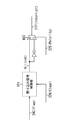
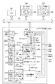
図2は、CPUに対する割り込み信号を生成するバスマスタ回路を備えたシステムLSIの構成の一例を示す図である。
図2において、システムLSIは、CPU201、バスマスタ回路202、外部通信モジュール203、及びシステムバス108を備えて構成される。尚、システムLSIには、これら以外に、例えばROMやRAM等も存在している。
バスマスタ回路202は、バスマスタ機能ブロック205、状態検出ブロック206、条件判定ブロック207、割り込み信号生成ブロック208、制御レジスタ群209、及びバススレーブ機能ブロック210を有する。このバスマスタ回路202は、割り込み信号(interrupt)217を生成し、生成した割り込み信号217を、システムバス108を介してCPU201に送信する。
FIG. 2 is a diagram illustrating an example of a configuration of a system LSI including a bus master circuit that generates an interrupt signal for the CPU.
In FIG. 2, the system LSI includes a
The
バスマスタ機能ブロック205は、システムバス108のバスプロトコルに従って、バスマスタとしてシステムバス108とアクセス(バスアクセス)するためのマスタインターフェースのブロックである。
状態検出ブロック206は、バスマスタ機能ブロック205にリード要求を行うリード要求制御ブロック206aと、バスマスタ機能ブロック205からリードデータを受信するレジスタ(DataReg)206bとを有する。また、状態検出ブロック206は、制御レジスタ群209から信号(En、Sts_Addr)221、222を受け取る。尚、信号(En、Sts_Addr)221、222の詳細については後述する。
The bus
The state detection block 206 includes a read
リード要求制御機能ブロック206aは、バスマスタ機能ブロック205とのインターフェースを有する。このリード要求制御機能ブロック206aは、リードリクエスト信号(req)232とアクセス終了信号(done)233とのハンドシェークで、アドレス信号(addr)231とリードデータ(rdata)234との受け渡しを行う。
The read request control function block 206 a has an interface with the bus
制御レジスタ群209のポーリング制御レジスタ211から送信された信号(En)221がポーリングの開始を示すものであるとき(En=0x1のとき)、リード要求制御機能ブロック206aは、バスマスタ機能ブロック205にリード要求を行う。具体的にリード要求制御機能ブロック206aは、ポーリングするターゲットとなるレジスタのアドレスを、ターゲットアドレスレジスタ212から出力された信号(Sts_Addr)222から読み取る。そして、リード要求制御機能ブロック206aは、リードリクエスト信号(req)232とアクセスアドレス信号(addr)231とをバスマスタ機能ブロック205に発行する。
When the signal (En) 221 transmitted from the polling control register 211 of the
また、リード要求制御機能ブロック206aは、アクセス終了信号(done)233とリードデータ(rdata)234とをバスマスタ機能ブロック205から受信する。リード要求制御機能ブロック206aは、受信したリードデータ(rdata)234を内部のレジスタ206bに格納する。尚、制御レジスタ群209のポーリング制御レジスタ211から送信された信号(En)221がポーリングの開始を示すものでないときは(En=0x0のときは)、リード要求制御機能ブロック206aは、リード要求を行わない。
Further, the read request control function block 206 a receives the access end signal (done) 233 and the read data (rdata) 234 from the bus
条件判定ブロック207は、状態検出ブロック206からレジスタ206bの出力信号(data)241を受け取り、その出力信号(data)241(すなわちリードデータ)と判定条件とを比較し、条件を満たしているか否かを判定するブロックである。そして、条件判定ブロック207は、判定した条件を満たしているか否かを示す条件判定フラグの信号(flag)242を生成する。また、条件判定ブロック207は、制御レジスタ群209の判定データレジスタ223から信号(Cond_Val)223を、判定マスクレジスタ214から信号(Cond_Mask)224を受け取る。尚、信号(Cond_Val、Cond_Mask)223、224の詳細については後述する。
The
図3は、条件判定ブロック207の構成の一例を示す図である。
図3において、比較器501は、排他的NOR回路で構成される。信号(raw_flag)511a〜511cは、信号(data)241a〜241cと、信号(Cond_Val)223a〜223cとのビット毎の比較の結果である。この比較の結果、信号(data)241a〜241cと、信号(Cond_Val)223a〜223cとが一致すれば、信号(raw_flag)511として「1」が出力される。一方、信号(data)241a〜241cと、信号(Cond_Val)223a〜223cとが不一致であれば、信号(raw_flag)511として「0」が出力される。
FIG. 3 is a diagram illustrating an example of the configuration of the
In FIG. 3, the
セレクタ502は、比較器501から出力された信号(raw_flag)511と、マスクデータである信号(Cond_Mask)224とを選択する。セレクタ502は、信号(Cond_Mask)224が「1」のときに、その信号(Cond_Mask)224を出力し、信号(raw_flag)511はマスクされる。一方、信号(Cond_Mask)224が「0」のとき、セレクタ502は、信号(raw_flag)511を出力する。論理積回路503は、セレクタ502から出力された信号の全ビットの論理積を演算する。論理積回路503は、演算した結果に基づく条件判定フラグを信号(flag)242として割り込み信号生成ブロック208に出力する。条件判定フラグは、信号(Cond_Mask)224でマスクされたビット以外の信号(raw_flag)511が全て「1」のときに「1」となり、それ以外のときには「0」となる。
The
図2に説明を戻し、割り込み信号生成ブロック208は、条件判定ブロック207から条件判定フラグの信号(flag)242を受け取り、割り込み信号(interrupt)217を生成するブロックである。また、制御レジスタ群209の信号生成制御レジスタ215から信号(Polarity)225を、クリアレジスタ216から信号(Clear)226を受け取る。尚、信号(Polarity、Clear)225、226の詳細については後述する。
Returning to FIG. 2, the interrupt
図4は、割り込み信号生成ブロック208の構成の一例を示す図である。
図4において、割り込み信号制御部601は、条件判定フラグの信号(flag)242から、正論理の割り込み信号(int)611を生成する。具体的に、クリアレジスタ216からの信号(Clear)226が「0」である場合、割り込み信号制御部601は、条件判定フラグの信号(flag)242から、正論理の割り込み信号(int)611を生成する(int=1)。一方、クリアレジスタ216からの信号(Clear)226が「0」である場合に、割り込み信号制御部601は、正論理の割り込み信号(int)611をネゲートする(int=0)。
FIG. 4 is a diagram illustrating an example of the configuration of the interrupt
In FIG. 4, the interrupt
セレクタ602は、割り込み信号制御部601から出力された割り込み信号(int)611の極性を選択する。セレクタ602は、信号(Polarity)225が「0」のとき、割り込み信号(interrupt)217として正論理の割り込み信号(int)611を出力する。一方、信号(Polarity)225が「1」のとき、セレクタ602は、割り込み信号(interrupt)217として正論理の割り込み信号(int)611を反転させた負論理の割り込み信号を出力する。
The
図2に説明を戻し、制御レジスタ群209は、状態検出ブロック206、条件判定ブロック207、及び割り込み信号生成ブロック208の動作を制御する信号のソースレジスタを有するブロックである。CPU201が各レジスタ211〜216の設定をプログラマブルに行う。
ポーリング制御レジスタ211は、ポーリングのスタート及びストップを制御するものであり、ポーリングのスタート、ストップを示す信号(En)221を状態検出ブロック206に出力する。図5(a)に、ポーリング制御レジスタ211の仕様の一例を示す。図5(a)において、Bitsはビット構成を示し、Nameは信号名を示し、Accessは属性を示し、Functionは機能を示す。ここで、属性のRはリードを示し、Wはライトを示す。ポーリング制御レジスタ211の0ビット目Enが「1」に設定されると、ポーリングをスタートさせる。すなわち、ポーリング制御レジスタ211は、「0x1」を示す信号(En)221を状態検出ブロック206に出力する。一方、ポーリング制御レジスタ211の0ビット目Enが「0」に設定されると、ポーリングをストップさせる。すなわち、ポーリング制御レジスタ211は、「0x0」を示す信号(En)221を状態検出ブロック206に出力する。
Returning to FIG. 2, the
The polling control register 211 controls the start and stop of polling, and outputs a signal (En) 221 indicating the start and stop of polling to the state detection block 206. FIG. 5A shows an example of the specification of the
ターゲットアドレスレジスタ212は、ポーリングするターゲットのレジスタ(例えばFIFOデータポインタレジスタ204)のアドレスを設定するものであり、そのアドレスを示す信号(Sts_Addr)222を状態検出ブロック206に出力する。図5(b)に、ターゲットアドレスレジスタ212の仕様の一例を示す。図5(b)に示すように、本実施形態では、信号(Sts_Addr)222を32ビットの構成としている。また、信号(Sts_Addr)222のビット幅を、使用するシステムバス108のアドレス幅と同じにしている。
The
判定データレジスタ213は、条件判定ブロック207における比較条件となるデータを設定するためのものであり、比較条件となるデータを示す信号(Cond_Val)223を条件判定ブロック207に出力する。図5(c)に、判定データレジスタ213の仕様の一例を示す。図5(c)に示すように、本実施形態では、信号(Cond_Val)223を32ビットの構成としている。また、信号(Cond_Val)223のビット幅を、使用するシステムバス108のデータ幅と同じにしている。
The determination data register 213 is for setting data as a comparison condition in the
判定データマスクレジスタ214は、条件判定をマスクするビットをビット毎に設定するためのものであり、その設定を示す信号(Cond_Mask)224を条件判定ブロック207に出力する。図5(d)に、判定データマスクレジスタ214の仕様の一例を示す。図5(d)に示すように、本実施形態では、信号(Cond_Mask)224を32ビットの構成としている。信号(Cond_Mask)224のビット幅を、使用するシステムバス108のデータ幅と同じにしている。図3に示したように、本実施形態では、信号(Cond_Mask)224を用いて、条件判定をマスクするビットをビット毎にマスクする。また、前述したように、該当するビットに対応する信号(Cond_Mask)224に「1」が設定されると、そのビットにおける条件判定がマスクされる。
The determination data mask
信号生成制御レジスタ215は、生成する割り込み信号(interrupt)217を制御するためのものであり、信号(Polarity)225を割り込み信号生成ブロック208に出力する。図5(e)に、信号生成制御レジスタ215の仕様の一例を示す。図5(e)に示すように、信号生成制御レジスタ215の0ビット目Polarityが「0」に設定されると、正論理の割り込み信号217が生成され、「1」に設定されると、負論理の割り込み信号217が生成される(図4を参照)。
The signal
クリアレジスタ216は、割り込み信号217をクリアするためのものであり、信号(Clear)226を割り込み信号生成ブロック208に出力する。図5(f)に、割り込みクリアレジスタ216の仕様の一例を示す。割り込みクリアレジスタ216の0ビット目Clearが「1」に設定されると、割り込み信号217がクリアされる。そして、割り込み信号217がクリアされると、割り込みクリアレジスタ216の0ビット目Clearは、自動的に「0」に戻る。
The
バススレーブ機能ブロック210は、CPU201が制御レジスタ群209にアクセスするためのインターフェースである。このバススレーブ機能ブロック210は、システムバス108のバスプロトコルに従って、バススレーブとしてシステムバス108とアクセス(バスアクセス)するためのスレーブインターフェースのブロックである。
The bus
外部通信モジュール203は、外部からのデータを送受信するブロックであり、データ受信用に1byte、16段のFIFO(First-In First-Out)を内蔵する。本実施形態では、FIFOに存在するデータ数を示すデータポインタレジスタ204が、アドレス「0xA000_0000」にマッピングされているとする。
図6は、データポインタレジスタ204の仕様の一例を示す図である。図6に示すように、4ビットのデータでFIFOに存在するデータ数を示し、データポインタレジスタ204の値は、「0x0」から「0xf」まで変化する。データポインタレジスタ204は、データを受信して、FIFOがフルになり、データポインタレジスタ204の値が「0xf」になると、正論理の割り込み信号(int_full)218を、システムバス108を介してCPU201に通知する。
The
FIG. 6 is a diagram illustrating an example of the specification of the data pointer register 204. As shown in FIG. 6, the number of data existing in the FIFO is indicated by 4-bit data, and the value of the data pointer register 204 changes from “0x0” to “0xf”. The data pointer register 204 receives data, and when the FIFO becomes full and the value of the data pointer register 204 becomes “0xf”, a positive logic interrupt signal (int_full) 218 is sent to the
次に、図2に示すシステムLSIの動作の一例について説明する。ここでは、バスマスタ回路202が、外部通信モジュール203のFIFOがフルになる一歩手前の状態(すなわち、データポインタレジスタ204の値が「0xe」となったこと)を検出して割り込み信号217を生成する場合を例に挙げて説明する。
Next, an example of the operation of the system LSI shown in FIG. 2 will be described. Here, the
まず、CPU201は、ポーリングするFIFOデータポインタレジスタ204のアドレス「0xA000_0000」をターゲットアドレスレジスタ212に設定する。これにより、ターゲットアドレスレジスタ212から出力される信号(Sts_Addr)222は、「0xA000_0000」を示す信号となる(Sts_Addr=0xA000_0000)。
次に、CPU201は、条件判定ブロック207における比較条件となるデータとして「0xe」を判定データレジスタ213に設定する。これにより、判定データレジスタ213から出力される信号(Cond_Val)223は、「0xe」を示す信号となる(Cond_Val=0xe)。
First, the
Next, the
またここでは、条件判定ブロック207で比較を行うデータは4ビットであるので、それ以外のビットの比較を行う必要はない。従って、その比較を行わないビットをマスクするために、CPU201は、「0xffff_fff0」を判定マスクレジスタ214に設定する。これにより、判定マスクレジスタ214から出力される信号(Cond_Mask)224は、「0xffff_fff0」を示す信号となる(Cond_Mask=0xffff_fff0)。
Here, since the data to be compared in the
次に、CPU201は、信号生成制御レジスタ215に「0x0」を設定する。これにより、信号生成制御レジスタ215から出力される信号225は、「0x0」を示す信号となる(Porality=0x0)。そして、CPU201は、ポーリング制御レジスタ211に「0x1」を設定する。これにより、ポーリング制御レジスタ211から状態検出ブロック206に出力される信号221は、「0x1」となり(En=0x1)、ポーリングがスタートする。
Next, the
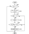
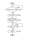
ポーリングがスタートすると、状態検出ブロック206はバスマスタ機能ブロック205にリード要求を行う。ここで、図7のフローチャートを参照しながら、バスマスタ機能ブロック205にリード要求を行う際の状態検出ブロック206の動作の一例を説明する。
まず、ステップS701において、リード要求制御機能ブロック206aは、ポーリング制御レジスタ211から出力された信号(En)221が「1」であるか否かを判断し、ポーリングをスタートする状態であるか否かを判断する。この判断の結果、ポーリングをスタートする状態でなければ、処理を終了する。一方、ポーリングをスタートする状態であれば、ステップS702に進む。
When polling starts, the state detection block 206 makes a read request to the bus
First, in step S701, the read request
ステップS702に進むと、リード要求制御機能ブロック206aは、ターゲットアドレスレジスタ212の設定値「0xA000_0000」をアドレス信号(addr)231とする。更にリード要求制御機能ブロック206aは、リードリクエスト信号(req)232をアサート(assert)する。すなわち、「1」を示すリードリクエスト信号(req)232をバスマスタ機能ブロック205に出力する(req=1)。
In step S702, the read request
次に、ステップS703において、リード要求制御機能ブロック206aは、アクセス終了信号(done)233がアサートされたか否かを判断する。すなわち、バスマスタ機能ブロック205から送信されたアクセス終了信号(done)233が「1」であるか否かを判断する。この判断の結果、アクセス終了信号(done)233がアサートされない場合(バスマスタ機能ブロック205から送信されたアクセス終了信号(done)233が「1」でない場合)には、処理を終了する。一方、アクセス終了信号(done)233がアサートされた場合(バスマスタ機能ブロック205から送信されたアクセス終了信号(done)233が「1」の場合)には、ステップS704に進む。
Next, in step S703, the read request
ステップS704に進むと、リード要求制御機能ブロック206aは、リードリクエスト信号(req)232をネゲート(negate)する。すなわち、「0」を示すリードリクエスト信号(req)232をバスマスタ機能ブロック205に出力する(req=0)。
次に、ステップS705において、リード要求制御機能ブロック206aは、バスマスタ機能ブロック205から出力されたリードデータ(rdata)234と、レジスタ206bに設定されているリードデータとを比較する。そして、リード要求制御機能ブロック206aは、リードデータに変化があるか否かを判断する。この判断の結果、リードデータに変化がない場合には処理を終了する。一方、リードデータに変化がある場合には、ステップS706に進む。ステップS706に進むと、リード要求制御機能ブロック206aは、バス機能ブロック205から出力されたリードデータ(rdata)234の値を、レジスタ206bに設定する。
In step S704, the read request
In step S705, the read request
図2に説明を戻し、外部通信モジュール203に内蔵されているFIFOにデータが溜まっていくと、レジスタ206bの値は、「0x0、0x1、・・・」と変化する。従って、条件判定ブロック207が入力する信号(data)241も、「0x0、0x1、・・・」と変化する。ここで、判定マスクレジスタ214から出力される信号(Cond_Mask)224は、「0xffff_fff0」である(Cond_Mask=0xffff_fff0)。従って、条件判定ブロック207が出力する条件判定フラグの信号(flag)242は、以下の(1)式が成り立つ間は「0」となる(flag=0)。また、条件判定フラグの信号(flag)242は、以下の(2)式が成り立つ間(すなわち、信号(data)241が「0xe」を示している間)は「1」となる(flag=1)。
data[3:0]≠Cond_Val[3:0] ・・・(1)
data[3:0]=Cond_Val[3:0] ・・・(2)
Returning to FIG. 2, when data accumulates in the FIFO built in the
data [3: 0] ≠ Cond_Val [3: 0] (1)
data [3: 0] = Cond_Val [3: 0] (2)
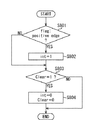
条件判定フラグの信号(flag)242が「1」になると(flag=1)、割り込み信号生成ブロック208の割り込み信号制御部601は正論理の割り込み信号(int)611を生成する(int=1)。ここで、図8のフローチャートを参照しながら、割り込み信号生成ブロック208の動作の一例を説明する。
When the condition determination flag signal (flag) 242 becomes “1” (flag = 1), the interrupt
まず、ステップS801において、割り込み信号制御部601は、条件判定フラグの信号(flag)242が立ち上がりエッジを有しているか否かを判断する。この判断の結果し、条件判定フラグの信号(flag)242が立ち上がりエッジを有していない場合には、ステップS802を省略して後述するステップS803に進む。一方、条件判定フラグの信号(flag)242が立ち上がりエッジを有している場合には、ステップS802に進む。
First, in step S801, the interrupt
ステップS802に進むと、割り込み信号制御部601は、正論理の割り込み信号(int)をアサートする(int=1)。
次に、ステップS803において、割り込み信号制御部601は、クリアレジスタ216からの信号(Clear)226がアサートされているか否か(クリアレジスタ216からの信号(Clear)226が「1」であるか否か)を判断する。この判断の結果、クリアレジスタ216からの信号(Clear)226がアサートされていない場合(クリアレジスタ216からの信号(Clear)226が「1」でない場合)には、処理を終了する。一方、クリアレジスタ216からの信号(Clear)226がアサートされている場合(クリアレジスタ216からの信号(Clear)226が「1」である場合)には、ステップS804に進む。
In step S802, the interrupt
In step S803, the interrupt
ステップS804に進むと、割り込み信号生成ブロック208は、正論理の割り込み信号(int)611と、クリアレジスタ216からの信号(Clear)226とをネゲートする(int=0、Clear=0)。
In step S804, the interrupt
図2に説明を戻し、クリアレジスタ216からの信号(Clear)226が「0」である場合には、割り込み信号制御部601は、正論理の割り込み信号(int)611を出力する(int=1)。ここでは、信号生成制御レジスタ215から出力された信号(Polarity)225が「0」に設定されている(Polarity=0x0)。従って、セレクタ602は、割り込み信号(interrupt)217として、正論理の割り込み信号(int)611を選択する。そして、セレクタ602は、「1」を示す割り込み信号(interrupt)217を、システムバス108を介してCPU201に出力する。
Returning to FIG. 2, when the signal (Clear) 226 from the
CPU201は、割り込み信号生成ブロック208から出力された割り込み信号(interrupt)217による割り込み通知を受けて、外部通信モジュール203に内蔵されているFIFOがフルになる一歩手前の状態で、所定の処理を行う。そして、CPU201は、割り込みをクリアする。割り込みのクリアは、割り込みクリアレジスタ216に「0x1」を設定することにより行われる。割り込みクリアレジスタ216に「0x1」が設定されると(Clear=0x1)、割り込み信号制御部601は、図8のフローチャートに従い、正論理の割り込み信号(int)611をネゲートする。これにより、「0」を示す割り込み信号(interrupt)217が出力され、割り込みがクリアされる。
The
以上のように本実施形態では、状態検出ブロック206が、外部通信モジュール203のFIFOにおけるデータ量を検出する。状態検出ブロック206の検出結果に基づいて、条件判定ブロック207が、割り込み信号217の生成条件を満たしているか否かを判定する。割り込み信号217の生成条件を満たしている場合に、割り込み信号生成ブロック208は、割り込み信号217を生成してCPU201に出力する。CPU201は、この割り込み信号217に基づいて、所定の処理を行う。
As described above, in the present embodiment, the state detection block 206 detects the data amount in the FIFO of the
従って、従来ではCPU201がポーリングを行って外部通信モジュール203の内部状態を検出しなければならない場合であっても、バスマスタ回路202がCPU201の代わりにポーリングを行い、CPU201に割り込み通知を行える。これにより、CPU201の負荷を削減できると共に、外部通信モジュール203の内部状態を検出する際の処理速度を向上させることができる。更に、プロセッサ(CPU)を複数設ける必要がないので、外部通信モジュール203の内部状態を検出するためのハードウェア(例えば複数のプロセッサの共有メモリ)によってシステムLSIの面積が増加することを防止できる。この他、状態検出ブロック206が状態の検出を行うハードウェアのアドレスと、条件判定ブロック207によって判定される条件とをプログラマブルに設定するようにしたので、様々なハードウェアの状態を様々な条件で判別することが可能となる。
Therefore, conventionally, even when the
尚、本実施形態では、バスマスタ回路202がポーリングする対象のハードウェアを外部通信モジュール203としたが、バスマスタ回路202がポーリングする対象はこれに限定されない。すなわち、ハードウェア内部に内部状態を表示するレジスタを備えたハードウェアモジュールであれば、どのようなハードウェアであってもポーリングする対象とすることができる。
また、CPU201は、各レジスタ211〜216に対してプログラマブルに設定を行うので、各レジスタ211〜216への設定の順番は、前述したものに限定されない。
In this embodiment, the hardware to be polled by the
In addition, since the
(第2の実施形態)
次に、本発明の第2の実施形態を説明する。本実施形態は、前述した第1の実施形態に、ポーリングするタイミングを調整する構成を追加したものである。従って、本実施形態の説明において、前述した第1の実施形態と同一の部分については、図1〜図8に付した符号と同一の符号を付す等して詳細な説明を省略する。尚、本実施形態でも、第1の実施形態と同様に、図1のハードウェア制御ブロック105を、システムバス108に接続されたCPU201に対する割り込み信号を生成する機能を有する割り込み信号生成ブロックで構成する場合を例に挙げて説明する。
(Second Embodiment)
Next, a second embodiment of the present invention will be described. In this embodiment, a configuration for adjusting the polling timing is added to the first embodiment described above. Therefore, in the description of the present embodiment, the same parts as those in the first embodiment described above are denoted by the same reference numerals as those in FIGS. In this embodiment as well, as in the first embodiment, the hardware control block 105 of FIG. 1 is configured with an interrupt signal generation block having a function of generating an interrupt signal for the
図9は、CPUに対する割り込み信号を生成するバスマスタ回路を備えたシステムLSIの構成の一例を示す図である。
バスマスタ回路202は、バスマスタ機能ブロック205、状態検出ブロック2206、条件判定ブロック207、制御信号生成ブロックとして割り込み信号生成ブロック208、制御レジスタ群2209、及びバススレーブ機能ブロック210を内蔵する。
FIG. 9 is a diagram illustrating an example of a configuration of a system LSI including a bus master circuit that generates an interrupt signal for the CPU.
The
状態検出ブロック2206は、第1の実施形態で説明したリード要求制御ブロック206a及びレジスタ(DataReg)206bと、ポーリング周期を計測するタイマー機能ブロック206cとを有する。
タイマー機能ブロック206cは、制御レジスタ群2209のポーリング周期設定レジスタ2217から、ポーリングを周期的に行うか否かを示す信号(Cyc_En)2227bを受け取る。また、タイマー機能ブロック206cは、ポーリングを周期的に行う場合には、その周期を示す信号(Cyc_Range)2227aを受け取る。尚、これらの信号(Cyc_Range、Cyc_En)2227の詳細については後述する。タイマー機能ブロック206cは、ポーリング周期設定レジスタ2217から出力された信号(Cyc_En)2227bが「0x1」を示すものである場合、リードリクエスト信号(req)232をアサートする間隔をタイマーで制御する。これにより、ポーリングの要求を周期的に行うことが可能になる。
The state detection block 2206 includes the read
The
制御レジスタ群2209は、状態検出ブロック2206、条件判定ブロック207、及び割り込み信号生成ブロック208の動作を制御する信号のソースレジスタを有するブロックである。CPU201が各レジスタ211〜216、2217の設定をプログラマブルに行う。
The
前述したように、ポーリング周期設定レジスタ2217は、ポーリングの周期設定を行うためのものであり、信号(Cyc_Range)2227a及び信号(Cyc_En)2227bを状態検出ブロック2206に出力する。図10は、ポーリング周期設定レジスタ2217の仕様の一例を示す図である。ポーリング周期設定レジスタ2217の0ビット目Cyc_Enが「1」に設定されると、周期的にポーリングを行う周期ポーリング動作モードとなる。また、ポーリング周期設定レジスタ2217の0ビット目Cyc_Enが「0」に設定されると、周期的でない通常のポーリングを行う通常ポーリング動作モードとなる。ポーリング周期設定レジスタ2217の0ビット目Cyc_Enを「1」に設定して周期ポーリング動作モードとする場合、ポーリング周期設定レジスタ2217の4〜31ビット目Cyc_Rangeにポーリングを行う周期が設定される。具体的にポーリング周期設定レジスタ2217の4〜31ビット目Cyc_Rangeにはポーリングする間隔として空けたい分のサイクル数が設定される。
As described above, the polling
次に、図9に示すシステムLSIの動作の一例について説明する。尚、本実施形態においても、外部通信モジュール203は、16段のFIFO(First-In First-Out)を内蔵するものとする。また、FIFOに存在するデータ数を示すデータポインタレジスタ204が、アドレス「0xA000_0000」にマッピングされているとする。また、バスマスタ回路2202が、外部通信モジュール203のFIFOがフルになる一歩手前の状態(すなわち、データポインタレジスタ204の値が「0xe」となったこと)を検出して割り込み信号217を生成するものとする。更に、状態検出ブロック2206が行うポーリングは3サイクル間隔で行われるものとする。
Next, an example of the operation of the system LSI shown in FIG. 9 will be described. Also in this embodiment, the
まず、CPU201は、ポーリングするFIFOデータポインタレジスタ204のアドレス「0xA000_0000」をターゲットアドレスレジスタ212に設定する。
次に、CPU201は、条件判定ブロック207における比較条件となるデータとして「0xe」を判定データレジスタ213に設定する。
First, the
Next, the
またここでは、条件判定ブロック207で比較を行うデータは4ビットであるので、それ以外のビットの比較を行う必要はない。従って、その比較を行わないビットをマスクするために、CPU201は、「0xffff_fff0」を判定マスクレジスタ214に設定する。
次に、CPU201は、信号生成制御レジスタ215に「0x0」を設定する。
Here, since the data to be compared in the
Next, the
更にここでは、3サイクル周期でポーリングを行うので、CPU201は、ポーリング周期設定レジスタ2217に「0x31」を設定する。これにより、ポーリング周期設定レジスタ2217から出力される信号(Cyc_Range)2227aは、「0x3」を示す信号となる(Cyc_Range=0x3)。また、信号(Cyc_En)2227bは、「0x1」を示す信号となる(Cyc_En=0x1)。
そして、CPU201は、ポーリング制御レジスタ211に「0x1」を設定して、ポーリングをスタートさせる。
Further, here, since polling is performed in a cycle of 3 cycles, the
Then, the
ポーリングがスタートすると、状態検出ブロック206はバスマスタ機能ブロック205にリード要求を行う。ここで、図11のフローチャートを参照しながら、バスマスタ機能ブロック205にリード要求を行う際の状態検出ブロック2206の動作の一例を説明する。
When polling starts, the state detection block 206 makes a read request to the bus
まず、ステップS1101〜S1106は、図7に示したステップS701〜706と同じである。すなわち、状態検出ブロック206は、ポーリングをスタートする状態であるか否かを判断する(ステップS1101)。そして、ポーリングをスタートする状態であれば、リード要求制御機能ブロック206aは、ターゲットアドレスレジスタ212の設定値「0xA000_0000」をアドレス信号(addr)231とする。更に、リード要求制御機能ブロック206aは、リードリクエスト信号(req)232をアサート(assert)する(ステップS1102)。
First, steps S1101 to S1106 are the same as steps S701 to 706 shown in FIG. That is, the state detection block 206 determines whether or not it is in a state of starting polling (step S1101). When the polling is started, the read request
次に、リード要求制御機能ブロック206aは、アクセス終了信号(done)233がアサートされたか否かを判断する(ステップS1103)。そして、アクセス終了信号(done)233がアサートされた場合、リード要求制御機能ブロック206aは、リードリクエスト信号(req)232をネゲート(negate)する(ステップS1104)。
Next, the read request
次に、リード要求制御機能ブロック206aは、リードデータに変化があるか否かを判断する(ステップS1105)。この判断の結果、リードデータに変化がない場合にはステップS1106を省略して後述するステップS1107に進む。一方、リードデータに変化がある場合には、リード要求制御機能ブロック206aは、バス機能ブロック205から出力されたリードデータ(rdata)234の値を、レジスタ206bに設定する。
Next, the read request
そして、ステップS1107に進むと、リード要求制御機能ブロック206aは、ポーリング周期設定レジスタ2217から出力された信号(Cyc_En)2227bの値を参照する。そして、リード要求制御機能ブロック206aは、動作モードが、周期ポーリング動作モード及び通常ポーリング動作モードの何れであるのかを判断する。この判断の結果、動作モードが通常ポーリング動作モードである場合には、処理を終了する。一方、動作モードが周期ポーリング動作モードである場合には、ステップS1108に進む。
In step S1107, the read request
ステップS1108に進むと、リード要求制御機能ブロック206aは、タイマー機能ブロック206cから信号(expired)2243がアサートされるまで待機する。すなわち、リード要求制御機能ブロック206aは、タイマー機能ブロック206cから、「1」を示す信号(expired)2243が出力されるまで待機する(expired=1)。
ここで、図12にタイミングチャートを参照しながら、次のポーリングの要求を3サイクル待たせる際の状態検出ブロック2206の動作の一例を説明する。
バスマスタ機能ブロック205からのアクセス終了信号(done)233を状態検出ブロック2206が受け取ると、次の処理を行う。すなわち、タイマー機能ブロック206cは、ポーリング周期設定レジスタ2217に設定されたサイクル数だけ、タイマーの値(timer)2244のデクリメントを開始する。
In step S1108, the read request
Here, an example of the operation of the state detection block 2206 when waiting for the next polling request for 3 cycles will be described with reference to the timing chart of FIG.
When the status detection block 2206 receives the access end signal (done) 233 from the bus
その後、タイマーの値(timer)2244が「0」になると、タイマー機能ブロック206cは、信号(expired)2243を1サイクルだけアサートする。信号(expired)2243がアサートされると、状態検出ブロック2206は、次のリードリクエスト信号(req)232をアサートする。これによりポーリングを行うことが可能となる。
尚、ポーリング周期設定レジスタ2217から出力された信号(Cyc_En)2227bが「0x0」の場合(Cyc_En=0x0)、状態検出ブロック2206は、このような周期的なポーリングを行わない。すなわち、状態検出ブロック2206は、アクセス終了信号(done)233がアサートされたらすぐに連続して次のポーリングの要求を発行する。
After that, when the timer value (timer) 2244 becomes “0”, the
If the signal (Cyc_En) 2227b output from the polling
図9に説明を戻し、外部通信モジュール203に内蔵されているFIFOにデータが溜まっていくと、レジスタ206bの値は、「0x0、0x1、・・・」と変化する。従って、条件判定ブロック207が入力する信号(data)241も、「0x0、0x1、・・・」と変化する。ここで、判定マスクレジスタ214から出力される信号(Cond_Mask)224は、「0xffff_fff0」である(Cond_Mask=0xffff_fff0)。従って、条件判定ブロック207が出力する条件判定フラグの信号(flag)242は、前記(1)式が成り立つ間は「0」となる(flag=0)。また、条件判定フラグの信号(flag)242は、前記(2)式が成り立つ間(すなわち、信号(data)241が「0xe」を示している間)は「1」となる(flag=1)。
Returning to FIG. 9, when data accumulates in the FIFO built in the
条件判定フラグの信号(flag)242が「1」になると(flag=1)、割り込み信号生成ブロック208の割り込み信号制御部601は正論理の割り込み信号(int)611を生成する(int=1)。尚、割り込み信号生成ブロック208の詳細な動作は、第1の実施形態で説明した通りである(図8を参照)。
When the condition determination flag signal (flag) 242 becomes “1” (flag = 1), the interrupt
そして、クリアレジスタ216からの信号(Clear)226が「0」である場合、割り込み信号制御部601は、正論理の割り込み信号(int)611を出力する(int=1)。ここでは、信号生成制御レジスタ215から信号(Polarity)225が「0」に設定されている(Polarity=0x0)。従って、セレクタ602は、割り込み信号(interrupt)217として、正論理の割り込み信号(int)611を選択する。そして、セレクタ602は、「1」を示す割り込み信号(interrupt)217を、システムバス108を介してCPU201に出力する。
When the signal (Clear) 226 from the
CPU201は、割り込み信号生成ブロック208から出力された割り込み信号(interrupt)217による割り込み通知を受けて、外部通信モジュール203に内蔵されているFIFOがフルになる一歩手前の状態で、所定の処理を行う。そして、CPU201は、割り込みをクリアする。割り込みのクリアは、割り込みクリアレジスタ216に「0x1」を設定することにより行われる。割り込みクリアレジスタ216に「0x1」が設定されると(Clear=0x1)、割り込み信号制御部601は、図8のフローチャートに従い、正論理の割り込み信号(int)611をネゲートする。これにより、「0」を示す割り込み信号(interrupt)217が出力され、割り込みがクリアされる。
The
以上のように本実施形態では、タイマー機能ブロック206cを用いて、ポーリング周期設定レジスタ2217に設定されている周期でポーリングの要求を行うようにした。従って、第1の実施形態で説明した効果に加え、システムバス108にかかる負荷をより軽減できるという効果を有する。
また、ポーリングの要求を行う周期をプログラマブルに設定するようにしたので、システムに応じてポーリング要求頻度を調整することができる。
尚、本実施形態では、周期的にポーリングの要求を行うようにしたが、ポーリングの要求が時間的に間隔を有して行われれば、必ずしも周期的にポーリングの要求を行う必要はない(すなわち、ポーリングの要求を行う間隔は一定でなくてもよい)。
As described above, in the present embodiment, the
In addition, since the period for performing the polling request is set programmably, the polling request frequency can be adjusted according to the system.
In this embodiment, the polling request is periodically made. However, if the polling request is made at intervals, it is not always necessary to make the polling request periodically (that is, The interval at which polling requests are made may not be constant).
(第3の実施形態)
次に、本発明の第3の実施形態について説明する。前述した第1及び第2の実施形態では、外部通信モジュール203の内部状態に応じて、バスマスタ回路202がCPU201に割り込み信号を通知するようにした。これに対し、本実施形態では、バスマスタ回路が、ポーリングを行ったハードウェアの内部状態に応じて、ポーリングを行っていない他のハードウェアへアクセスするようにしている。このように、本実施形態と前述した第1及び第2の実施形態とは、バスマスタ回路の構成の一部、バスマスタ回路がポーリングするハードウェア、及びポーリングを行った後にバスマスタ回路がアクセスするハードウェアとが異なる。従って、本実施形態の説明において、前述した第1及び第2の実施形態と同一の部分については、図1〜図12に付した符号と同一の符号を付す等して詳細な説明を省略する。尚、本実施形態では、図1に示したハードウェア制御ブロック105を、クロック制御モジュールのレジスタの設定を行うバス転送制御ブロックで構成する場合を例に挙げて説明する。
(Third embodiment)
Next, a third embodiment of the present invention will be described. In the first and second embodiments described above, the
図13は、クロック制御モジュールのレジスタの設定を行うバスマスタ回路を備えたシステムLSIの構成の一例を示す図である。
図13において、システムLSIは、CPU201、バスマスタ回路3202、ポート制御モジュール1203、及びクロック制御モジュール1205を備えて構成される。
バスマスタ回路3202は、バスマスタ機能ブロック3205、状態検出ブロック206、条件判定ブロック207、バス転送制御ブロック1208、制御レジスタ群3209、及びバススレーブ機能ブロック210を内蔵する。本実施形態では、バス転送制御ブロック1208が、クロック制御モジュール1205のレジスタの設定を行う。
FIG. 13 is a diagram illustrating an example of a configuration of a system LSI including a bus master circuit for setting a register of the clock control module.
In FIG. 13, the system LSI includes a
The bus master circuit 3202 includes a bus
バスマスタ機能ブロック3205は、システムバス108のバスプロトコルに従って、バスマスタとしてシステムバス108とアクセス(バスアクセス)するためのマスタインターフェースのブロックである。
The bus
状態検出ブロック206は、前述したように、システムバスに接続されたハードウェアの内部状態を検出する。本実施形態では、状態検出ブロック206は、ポートステータスレジスタ1205の内部状態を検出する。
条件判定ブロック207は、前述したように、状態検出ブロック206の検出結果に基づいて、条件を満たしているか否かを判定する。本実施形態では、条件判定ブロック207は、クロックコントロールレジスタ1206へ書き込みを行うための条件を満たしているか否かを判定する。
As described above, the state detection block 206 detects the internal state of the hardware connected to the system bus. In the present embodiment, the state detection block 206 detects the internal state of the
As described above, the
バス転送制御ブロック1208は、条件判定ブロック207から、条件判定フラグの信号(flag)242の立ち上がりエッジを受け取り、バスマスタ機能ブロック3205に、クロックコントロールレジスタ1206への書き込み要求を行う。以下の説明では、クロックコントロールレジスタ1206への書き込み要求を必要に応じてライト転送の要求と称する。
The bus
バス転送制御ブロック1208は、バスマスタ機能ブロック3205とのインターフェースを有する。バス転送制御ブロック1208は、ライトリクエスト信号(req)3232とアクセス終了信号(done)3233のハンドシェークで、アドレス信号(addr)3231とライトデータ(wdata)3234をバスマスタ機能ブロック3235に渡す。また、バス転送制御ブロック1208は、制御レジスタ群209から、信号(Trf_Addr、Trf_Val)3216、3217を受け取る。この信号(Trf_Addr、Trf_Val)3216、3217の詳細については後述する。更に、バス転送制御ブロック1208は、状態検出ブロック206によるポーリング動作を停止させる場合に、ポーリング制御レジスタ211へ信号(Clear)3226を出力する。
The bus
制御レジスタ群3209は、状態検出ブロック206、条件判定ブロック207、及びバス転送制御ブロック1208の動作を制御する信号のソースレジスタを有するブロックである。CPU201が各レジスタ212〜214、1216〜1218の設定をプログラマブルに行う。
The control register group 3209 is a block having a source register of signals for controlling operations of the state detection block 206, the
ポーリング制御レジスタ1218は、ポーリングのスタート及びストップを制御するためのものであり、ポーリングのスタート、ストップを示す信号(En)221を状態検出ブロック206に出力する。ポーリング制御レジスタ1218の仕様は、図5(a)に示したポーリング制御レジスタ211と同じである。ただし、ポーリング制御レジスタ1218は、バス転送制御ブロック1208から信号(Clear)3226を受け取った場合にも、ポーリングをストップさせる。すなわち、ポーリング制御レジスタ1218は、「0x0」を示す信号(En)221を状態検出ブロック206に出力する。
The
ターゲットアドレスレジスタ212は、前述したように、ポーリングするターゲットとなるレジスタのアドレスを設定するためのものであり、その仕様は、図5(b)に示した通りである。本実施形態では、ターゲットアドレスレジスタ212は、図13に示すポートステータスレジスタ1204のアドレスを設定する。
判定データレジスタ213は、前述したように、条件判定ブロック207における比較条件となるデータを設定するためのものであり、その仕様は、図5(c)に示した通りである。
判定データマスクレジスタ214は、前述したように、条件判定をマスクするビットをビット毎に設定するためのものであり、その仕様は、図5(d)に示した通りである。
As described above, the
As described above, the determination data register 213 is used to set data as a comparison condition in the
As described above, the determination data mask
転送アドレスレジスタ1216は、ポーリングを行うモジュールとは異なるモジュールのレジスタであって、データの書き換え対象となるレジスタのアドレスを設定するものである。この転送アドレスレジスタ1216は、そのアドレスを示す信号(Trf_Addr)3216をバス転送制御ブロック1208に出力する。図14(a)に、転送アドレスレジスタ1216の仕様の一例を示す。図14(a)に示すように、本実施形態では、信号(Trf_Addr)3216を32ビットの構成としている。また、信号(Trf_Addr)3216のビット幅を、使用するシステムバス108のアドレス幅と同じにしている。
The transfer address register 1216 is a register of a module different from the module that performs polling, and sets the address of a register to be rewritten. The transfer address register 1216 outputs a signal (Trf_Addr) 3216 indicating the address to the bus
転送データレジスタ1217は、データの書き換え対象のレジスタに書き込むデータを設定するものである。この転送データレジスタ1217は、そのデータを示す信号(Trf_Val)3217をバス転送制御ブロック1208に出力する。図14(b)に、転送データレジスタ1217の仕様の一例をに示す。図14(b)に示すように、本実施形態では、信号(Trf_Val)3217を32ビットの構成としている。また、信号(Trf_Val)3217のビット幅を、使用するシステムバス108のデータ幅と同じにしている。
バススレーブ機能ブロック210は、前述したように、CPU201が制御レジスタ群209にアクセスするためのインターフェースである。
The transfer data register 1217 sets data to be written in a register to be rewritten. The transfer data register 1217 outputs a signal (Trf_Val) 3217 indicating the data to the bus
As described above, the bus
ポート制御モジュール1203は、システムLSIの外部端子において汎用ポートとして割り当てられているポートの制御を行う。このポート制御モジュール1203は、外部端子の状態を示すポートステータスレジスタ1204を持つ。本実施形態では、ポートステータスレジスタ1204が、アドレス「0xA010_0000」にマッピングされているとする。図15(a)は、ポートステータスレジスタ1204の仕様の一例を示す図である。図15(a)に示すように、0ビット目〜7ビット目P0_Sts〜P7_Stsのそれぞれにおいて、外部端子P0〜P7の状態をポートステータスレジスタ1204から読み出すことができる。尚、ポートステータスレジスタ1204の設定は、例えばCPU201によってプログラマブルに行われる。
The
クロック制御モジュール1205は、システムLSIの各モジュールに供給されるクロックの制御を行う。このクロック制御モジュール1205は、各モジュールのクロックの設定を行うクロックコントロールレジスタ1206を持つ。本実施形態では、クロックコントロールレジスタ1206が、アドレス「0xA020_0000」にマッピングされているとする。
The
図15(b)は、クロックコントロールレジスタ1206の仕様の一例を示す図である。図15(b)に示すように、0ビット目CPU_clkに「1」が設定されると、CPU201にクロックが供給される。一方、0ビット目CPU_clkに「0」が設定されると、CPU201にクロックが供給されなくなる。尚、システムの起動時には、0ビット目CPU_clkに「1」が設定され、CPU201にクロックが供給された状態になる。
また、1〜2ビット目CPU_clk_frqに「0」が設定されると、CPU201のクロックの周波数は1MHzとなる。同様に、1〜2ビット目CPU_clk_frqに「1」が設定されると8MHz、「2」が設定されると64MHz、「3」が設定されると128MHzとなる。
FIG. 15B is a diagram illustrating an example of the specification of the
When “0” is set in the CPU_clk_frq for the first and second bits, the clock frequency of the
次に、図14に示すシステムLSIの動作の一例について説明する。ここでは、CPU201のクロックを停止させて、低消費電力状態へシステムを移行させた後、外部端子の状態をポーリングして通常動作状態へ復帰させる場合を例に挙げて説明する。尚、通常動作状態への復帰は、外部端子P6、P7に対する設定が共に「1」になったときに行うとする。
Next, an example of the operation of the system LSI shown in FIG. 14 will be described. Here, the case where the clock of the
まず、CPU201は、バスマスタ回路202の制御レジスタ群209に対する設定を行う。具体的にCPU201は、ポーリングする対象であるポートステータスレジスタ1204のアドレス「0xA010_0000」をターゲットアドレスレジスタ212に設定する。これにより、ターゲットアドレスレジスタ212から出力される信号(Sts_Addr)222は、「0xA010_0000」を示す信号となる(Sts_Addr=0xA000_0000)。
次に、CPU201は、条件判定ブロック207における比較条件となるデータとして「0xc0」を判定データレジスタ213に設定する。これにより、判定データレジスタから出力される信号(Cond_Val)223は、「0xc0」を示す信号となる(Cond_Val=0xc0)。
First, the
Next, the
また、条件判定ブロック207で比較を行うデータは、6ビット目と7ビット目の2ビットであるので、それ以外のビットの比較を行う必要はない。従って、その比較を行わないビットをマスクするために、CPU201は、「0xffff_ff3f」を判定マスクレジスタ214に設定する。これにより、判定マスクレジスタ214から出力される信号(Cond_Mask)224は、「0xffff_ff3f」を示す信号となる(Cond_Mask=0xffff_ff3f)。
Further, since the data to be compared in the
そして、CPU201は、データの書き換え対象となるクロックコントロールレジスタ1206のアドレス「0xA020_0000」を転送アドレスレジスタ1216に設定する。これにより、クロックコントロールレジスタ1206から出力される信号(Trf_Addr)3216は、「0xA020_0000」を示す信号となる(Trf_Addr=0xA020_0000)。
次に、CPU201は、CPU201へクロックを供給し、クロック周波数を1MHzにするデータ「0x1」を転送データレジスタ1217に設定する。これにより、転送データレジスタ1217から出力される信号(Trf_Val)3217は、「0x1」となる(Trf_Val=0x1)。
そして、CPU201は、ポーリング制御レジスタ211に「0x1」を設定する。これにより、ポーリング制御レジスタ211から出力される信号221は、「0x1」となり(En=0x1)、ポーリングがスタートする。
Then, the
Next, the
Then, the
その後、CPU201は、バスマスタ回路202を動作させた後、クロックコントロールレジスタ1206の0ビット目CPU_clkを「0」に設定する。そうすると、CPU201へクロックが供給されなくなり、低消費電力状態へ移行する。
Thereafter, after operating the
ポーリング制御レジスタ211から出力された信号(En)221が「0x1」になると(En=0x1)、状態検出ブロック206は、バスマスタ機能ブロック205にリード要求を行う。状態検出ブロック206がバスマスタ機能ブロック205にリード要求を行う際の動作は、図7に示した通りである。
When the signal (En) 221 output from the
そして、バスマスタ機能ブロック3205によるポートステータスレジスタ1204のポーリングの結果によって得られる外部端子P0〜P7の変化に応じて、レジスタ206bの値は、「0x13、0x19、・・・」と変化する。従って、条件判定ブロック207が入力する信号(data)241も、「0x13、0x19、・・・」と変化する。ここで、判定マスクレジスタ214から出力される信号(Cond_Mask)224は、「0xffff_ff3f」である(Cond_Mask=0xffff_ff3f)。従って、条件判定ブロック207が出力する条件判定フラグの信号(flag)242は、以下の(3)式が成り立つ間は「0」であり(flag=0)、以下の(4)式が成り立つ間は「1」となる(flag=1)。
data[7:6]≠Cond_Val[7:6] ・・・(3)
data[7:6]=Cond_Val[7:6](data[7:6]=b11(2進数)) ・・・(4)
Then, the value of the
data [7: 6] ≠ Cond_Val [7: 6] (3)
data [7: 6] = Cond_Val [7: 6] (data [7: 6] = b11 (binary number)) (4)
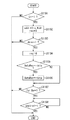
条件判定フラグの信号(flag)242が「1」になると(flag=1)、バス転送制御ブロック1208は、バスマスタ機能ブロック205にライト転送の要求を行うと共に、信号(Clear)3226をポーリング制御レジスタ211へ出力する。ここで、図16のフローチャートを参照しながら、バスマスタ機能ブロック205へのライト転送の要求と、ポーリング制御レジスタ211への信号(Clear)3226の出力とを行う際のバス転送制御ブロック1208の動作の一例を説明する。
When the signal (flag) 242 of the condition determination flag becomes “1” (flag = 1), the bus
まず、ステップS1601において、バス転送制御ブロック1208は、条件判定フラグの信号(flag)242が立ち上がりエッジを有しているか否かを判断する。この判断の結果、条件判定フラグの信号(flag)242が立ち上がりエッジを有していない場合には、条件判定フラグの信号(flag)242が立ち上がりエッジを有するまで待機する。一方、条件判定フラグの信号(flag)242が立ち上がりエッジを有している場合には、ステップS1602に進む。
First, in step S1601, the bus
ステップS1602に進むと、バス転送制御ブロック1208は、ポーリング動作を停止させるために、信号(Clear)3226をポーリング制御レジスタ1218に出力する。
次に、ステップS1602において、バス転送制御ブロック1208は、転送アドレスレジスタ212の設定値「0xA020_0000」をアドレス信号(addr)に含める。また、バス転送制御ブロック1208は、ライトデータ(wdata)3234に転送データレジスタの設定値「0x1」を含める。そして、バス転送制御ブロック1208は、ライトリクエスト信号(req)3232をアサートする(req=1)。すなわち、バス転送制御ブロック1208は、「1」を示すライトリクエスト信号(req)3232をバスマスタ機能ブロック3205に出力する。これにより、バス転送制御ブロック1208からバスマスタ機能ブロック205へ、ライト転送の要求がなされる。
In step S1602, the bus
Next, in step S1602, the bus
次に、ステップS1604において、バス転送制御ブロック1208は、アクセス終了信号(done)3233がアサートされたか否かを判断する。すなわち、バス転送制御ブロック1208は、バスマスタ機能ブロック205から送信されたアクセス終了信号(done)3233が「1」であるか否かを判断する。この判断の結果、アクセス終了信号(done)3233がアサートされない場合(バスマスタ機能ブロック3205から送信されたアクセス終了信号(done)3233が「1」でない場合)には、アサートされるまで待機する。一方、アクセス終了信号(done)3233がアサートされた場合(バスマスタ機能ブロック3205から送信されたアクセス終了信号(done)3233が「1」の場合)には、ステップS1605に進む。
Next, in step S1604, the bus
ステップS1605に進むと、バス転送制御ブロック1208は、リードリクエスト信号(req)3232をネゲート(negate)する。すなわち、バス転送制御ブロック1208は、「0」を示すリードリクエスト信号(req)3232をバスマスタ機能ブロック3205に出力する(req=0)。
In step S1605, the bus
以上のようにしてバス転送制御ブロック1208からバスマスタ機能ブロック3205になされたライト転送の要求により、バスマスタ機能ブロック3205は、クロック制御モジュール1205にライト転送を行う。そうすると、クロックコントロールレジスタ1206に「0x1」が設定され、CPU201に1MHzのクロックが供給され、通常動作状態へ復帰する。
In response to the write transfer request made from the bus
以上のように本実施形態では、状態検出ブロック3206が、ポートステータスレジスタ1204の設定をポーリングし、外部端子P0〜P7の状態を検出する。状態検出ブロック3206の検出結果に基づいて、条件判定ブロック207は、低消費電力状態から通常動作状態にシステムを復帰させるための条件を満たしているか否かを判定する。低消費電力状態から通常動作状態にシステムを復帰させるための条件を満たすと、バス転送制御ブロック1208は、クロックコントロールレジスタ1206への書き込み要求(ライト転送の要求)をバスマスタ機能ブロック3205に行う。バスマスタ機能ブロック3205は、バス転送制御ブロック1208からなされたライト転送の要求に従って、クロックコントロールレジスタ1206の書き換え指示(ライト転送)を行う。クロック制御モジュール1205は、クロックコントロールレジスタ1206は、ライト転送に従ってクロックコントロールレジスタ1206の設定値を変更する。そうすると、CPU201は、その変更に従って、低消費電力状態から通常動作状態にシステムを復帰させる。
As described above, in this embodiment, the state detection block 3206 polls the setting of the
以上のようにすることによって、バスマスタ回路3202は、低消費電力状態でCPU201が停止している状況でも、CPU201に代わりにポートステータスレジスタ1204をポーリングして通常動作状態へ復帰する条件が成立したことを検出できる。そして、バスマスタ回路3202がクロックコントロールレジスタ1206の設定を行うことができる。従って、CPU201への割り込み処理を行わずにクロックコントロールレジスタ1206の設定を行って、通常動作状態へ復帰させることができる。これにより、CPU201の負荷を削減できると共に、ポート制御モジュール1203(ポートステータスレジスタ1204)の内部状態を検出する際の処理速度を向上させることができる。更に、プロセッサ(CPU)を複数設ける必要がないので、ポート制御モジュール1203(ポートステータスレジスタ1204)の内部状態を検出するためのハードウェアによってシステムLSIの面積が増加することを防止できる。この他、データの書き換え対象となるレジスタのアドレスと、データの内容とをプログラマブルに設定するようにしたので、様々なハードウェアを様々な形態で制御することが可能になる。
As a result, the bus master circuit 3202 satisfies the condition that the
尚、本実施形態では、バスマスタ回路3202がポーリングする対象のハードウェアをポート制御モジュール1203としたが、第1及び第2の実施形態と同様に、バスマスタ回路3202がポーリングする対象はこれに限定されない。すなわち、ハードウェア内部に内部状態を表示するレジスタを備えたハードウェアモジュールであれば、どのようなハードウェアであってもポーリングする対象とすることができる。
In this embodiment, the hardware to be polled by the bus master circuit 3202 is the
また、本実施形態では、設定対象のレジスタをクロック制御モジュール1205内のクロックコントロールレジスタ1206としたが、設定対象のレジスタはこれに限定されない。すなわち、バス転送により設定が可能なレジスタを有するハードウェアモジュールであれば、どのようなハードウェアモジュール内のレジスタであっても設定対象とすることができる。
In this embodiment, the setting target register is the
また、本実施形態では、バス転送制御ブロック1208がライト転送をバスマスタ機能ブロック3205に要求するようにしたが、必ずしもライト転送を要求しなくてもよい。例えば、ハードウェアモジュールの内部状態の読み出しの要求(リード転送の要求)を行ってもよい。また、リード転送を行うことによって読み出されたデータに応じて所定のビットを対象に操作を行ったデータの書き込みの要求(read-modify-write転送の要求)を行ってもよい。また、通常動作状態時にCPU201がプログラマブルにクロックコントロールレジスタ1206の設定を行えるようにしてもよい。
また、転送アドレスレジスタ1216及び転送データレジスタ1217を複数設け、バス転送制御ブロック1208が複数のレジスタを設定対象としてライト要求等を行えるようにしてもよい。
In this embodiment, the bus
A plurality of transfer address registers 1216 and transfer data registers 1217 may be provided so that the bus
また、第2の実施形態と同様に、ポーリング周期設定レジスタ2217とタイマー機能ブロック206cとを設け、ポーリング周期設定レジスタ2217に設定されている周期でポーリングの要求を行うようにしてもよい。このようにすれば、システムバス108にかかる負荷をより軽減することができる。
また、本実施形態では、転送方向レジスタを更に設け、この転送方向レジスタを用いることにより転送方向をプログラマブルに設定することもできる。
Similarly to the second embodiment, a polling
In this embodiment, a transfer direction register is further provided, and the transfer direction can be set programmable by using this transfer direction register.
(本発明の他の実施形態)
前述した実施形態の機能を実現するべく各種のデバイスを動作させるように、該各種デバイスと接続された装置あるいはシステム内のコンピュータに対し、前記実施形態の機能を実現するためのソフトウェアのプログラムコードを供給してもよい。そのシステムあるいは装置のコンピュータ(CPUあるいはMPU)に格納されたプログラムに従って前記各種デバイスを動作させることによって実施したものも、本発明の範疇に含まれる。
(Other embodiments of the present invention)
In order to operate various devices to realize the functions of the above-described embodiments, program codes of software for realizing the functions of the above-described embodiments are provided to an apparatus or a computer in the system connected to the various devices. You may supply. What was implemented by operating said various devices according to the program stored in the computer (CPU or MPU) of the system or apparatus is also included in the category of the present invention.
また、この場合、前記ソフトウェアのプログラムコード自体が前述した実施形態の機能を実現することになる。また、そのプログラムコード自体、及びそのプログラムコードをコンピュータに供給するための手段、例えば、かかるプログラムコードを格納した記録媒体は本発明を構成する。かかるプログラムコードを記憶する記録媒体としては、例えばフレキシブルディスク、ハードディスク、光ディスク、光磁気ディスク、CD−ROM、磁気テープ、不揮発性のメモリカード、ROM等を用いることができる。 In this case, the program code of the software itself realizes the functions of the above-described embodiment. The program code itself and means for supplying the program code to a computer, for example, a recording medium storing the program code constitute the present invention. As a recording medium for storing the program code, for example, a flexible disk, a hard disk, an optical disk, a magneto-optical disk, a CD-ROM, a magnetic tape, a nonvolatile memory card, a ROM, or the like can be used.
また、コンピュータが供給されたプログラムコードを実行することにより、前述の実施形態の機能が実現されるだけでない。そのプログラムコードがコンピュータにおいて稼働しているオペレーティングシステムあるいは他のアプリケーションソフト等と共同して前述の実施形態の機能が実現される場合にもかかるプログラムコードは本発明の実施形態に含まれることは言うまでもない。 Further, the functions of the above-described embodiments are not only realized by executing the program code supplied by the computer. It goes without saying that the program code is also included in the embodiment of the present invention even when the function of the above-described embodiment is realized in cooperation with an operating system or other application software running on the computer. Yes.
さらに、供給されたプログラムコードがコンピュータの機能拡張ボードに備わるメモリに格納された後、そのプログラムコードの指示に基づいてその機能拡張ボードに備わるCPUが実際の処理の一部または全部を行う。その処理によって前述した実施形態の機能が実現される場合にも本発明に含まれることは言うまでもない。
また、供給されたプログラムコードがコンピュータに接続された機能拡張ユニットに備わるメモリに格納された後、そのプログラムコードの指示に基づいて機能拡張ユニットに備わるCPU等が実際の処理の一部または全部を行う。その処理によって前述した実施形態の機能が実現される場合にも本発明に含まれることは言うまでもない。
Further, after the supplied program code is stored in the memory provided in the function expansion board of the computer, the CPU provided in the function expansion board performs part or all of the actual processing based on the instruction of the program code. Needless to say, the present invention includes the case where the functions of the above-described embodiments are realized by the processing.
Further, after the supplied program code is stored in the memory provided in the function expansion unit connected to the computer, the CPU or the like provided in the function expansion unit performs part or all of the actual processing based on the instruction of the program code. Do. Needless to say, the present invention includes the case where the functions of the above-described embodiments are realized by the processing.
なお、前述した各実施形態は、何れも本発明を実施するにあたっての具体化の例を示したものに過ぎず、これらによって本発明の技術的範囲が限定的に解釈されてはならないものである。すなわち、本発明はその技術思想、またはその主要な特徴から逸脱することなく、様々な形で実施することができる。 Note that each of the above-described embodiments is merely a specific example for carrying out the present invention, and the technical scope of the present invention should not be construed as being limited thereto. . That is, the present invention can be implemented in various forms without departing from the technical idea or the main features thereof.
101、202、2202、3202 バスマスタ回路
102、205、3205 バスマスタ機能ブロック
103、206、2206 状態検出ブロック
104、207 条件判定ブロック
105 ハードウェア制御ブロック
106、209、2209、3209 制御レジスタ群
107、210 バススレーブ機能ブロック
108 システムバス
201 CPU
203 外部通信モジュール
204 FIFOデータポインタレジスタ
208 割り込み信号生成ブロック
1203 ポート制御モジュール
1204 ポートステータスレジスタ
1205 クロック制御モジュール
1206 クロックコントロールレジスタ
1208 バス転送制御ブロック
101, 202, 2202, 3202
203 External Communication Module 204 FIFO
Claims (23)
前記バスにバスマスタとしてアクセスして、前記バスを介して相互に接続されたハードウェアの状態を検出する検出手段と、
前記検出手段により検出されたハードウェアの状態を判別する判別手段と、
前記判別手段により判別されたハードウェアの状態に基づいて制御信号を生成する生成手段と、
前記生成手段により生成された制御信号を前記バスに出力する出力手段とを有することを特徴とするバスマスタ回路。 A bus master circuit interconnected with a processor and one or more hardware via a bus,
Detecting means for accessing the bus as a bus master and detecting a state of hardware connected to each other via the bus;
Discriminating means for discriminating the state of the hardware detected by the detecting means;
Generating means for generating a control signal based on the hardware state determined by the determining means;
An output means for outputting the control signal generated by the generating means to the bus.
前記出力手段は、前記生成手段により生成された割り込み信号を、前記バスを介して、前記プロセッサに出力することを特徴とする請求項1に記載のバスマスタ回路。 The generation unit generates an interrupt signal for processors connected to each other via the bus based on the hardware state determined by the determination unit;
The bus master circuit according to claim 1, wherein the output unit outputs the interrupt signal generated by the generation unit to the processor via the bus.
前記出力手段は、前記生成手段により生成された制御信号を、前記バスを介して、前記第2のハードウェアに出力することを特徴とする請求項1に記載のバスマスタ回路。 The generation unit generates a control signal related to the operation of the second hardware different from the hardware based on the hardware state determined by the determination unit;
The bus master circuit according to claim 1, wherein the output unit outputs the control signal generated by the generation unit to the second hardware via the bus.
前記検出手段は、バスを介して相互に接続されたハードウェアの状態を前記間隔設定手段に設定された間隔で検出することを特徴とする請求項5に記載のバスマスタ回路。 An interval setting means in which an interval for detecting the state of hardware connected to each other via the bus is set in a programmable manner;
6. The bus master circuit according to claim 5, wherein the detection unit detects a state of hardware connected to each other via a bus at an interval set in the interval setting unit.
前記制御信号に含めるデータがプログラマブルに設定されるデータ設定手段とを有し、
前記生成手段は、前記データ設定手段に設定されたデータを含む制御信号を生成し、
前記出力手段は、前記バスを介して、前記出力先アドレス設定手段に設定されたアドレスに、前記生成手段により生成された制御信号を出力することを特徴とする請求項7に記載のバスマスタ回路。 Output destination address setting means in which an output destination address of the control signal is set in a programmable manner;
Data setting means in which data included in the control signal is set in a programmable manner;
The generating means generates a control signal including data set in the data setting means,
8. The bus master circuit according to claim 7, wherein the output unit outputs the control signal generated by the generation unit to the address set in the output destination address setting unit via the bus.
前記検出手段は、前記ハードウェアアドレス設定手段に設定されたアドレスのハードウェアの状態を検出することを特徴とする請求項1〜9の何れか1項に記載のバスマスタ回路。 A hardware address setting unit in which a hardware address detected by the detection unit is set in a programmable manner;
The bus master circuit according to claim 1, wherein the detection unit detects a hardware state of an address set in the hardware address setting unit.
前記判別手段は、前記検出手段により検出されたハードウェアの状態が、前記条件設定手段に設定された条件に該当するか否かを判別することを特徴とする請求項1〜10の何れか1項に記載のバスマスタ回路。 Having condition setting means in which a condition for determining the state of the hardware detected by the detection means is set in a programmable manner;
11. The determination unit according to claim 1, wherein the determination unit determines whether a hardware state detected by the detection unit corresponds to a condition set in the condition setting unit. The bus master circuit according to item.
前記検出ステップにより検出されたハードウェアの状態を判別する判別ステップと、
前記判別ステップにより判別されたハードウェアの状態に基づいて制御信号を生成する生成ステップと、
前記生成ステップにより生成された制御信号を前記バスに出力する出力ステップとを有することを特徴とするバス制御方法。 A detection step of accessing the bus as a bus master and detecting the state of hardware interconnected via the bus;
A determination step of determining the state of the hardware detected by the detection step;
A generation step of generating a control signal based on the hardware state determined by the determination step;
A bus control method comprising: an output step of outputting the control signal generated in the generation step to the bus.
前記出力ステップは、前記生成ステップにより生成された割り込み信号を、前記バスを介して、前記プロセッサに出力することを特徴とする請求項12に記載のバス制御方法。 The generation step generates an interrupt signal for processors connected to each other via the bus based on the hardware state determined by the determination step;
13. The bus control method according to claim 12, wherein the output step outputs the interrupt signal generated by the generation step to the processor via the bus.
前記出力ステップは、前記生成ステップにより生成された制御信号を、前記バスを介して、前記第2のハードウェアに出力することを特徴とする請求項12に記載のバス制御方法。 The generation step generates a control signal related to the operation of second hardware different from the hardware based on the hardware state determined by the determination step;
13. The bus control method according to claim 12, wherein the output step outputs the control signal generated by the generation step to the second hardware via the bus.
前記検出ステップは、バスを介して相互に接続されたハードウェアの状態を前記間隔設定ステップにより設定された間隔で検出することを特徴とする請求項16に記載のバス制御方法。 An interval setting step for programmably setting an interval for detecting the state of hardware connected to each other via the bus;
17. The bus control method according to claim 16, wherein the detecting step detects a state of hardware connected to each other via a bus at an interval set by the interval setting step.
前記制御信号に含めるデータをプログラマブルに設定するデータ設定ステップとを有し、
前記生成ステップは、前記データ設定ステップにより設定されたデータを含む制御信号を生成し、
前記出力ステップは、前記バスを介して、前記出力先アドレス設定ステップにより設定されたアドレスに、前記生成ステップにより生成された制御信号を出力することを特徴とする請求項18に記載のバス制御方法。 An output destination address setting step for programmably setting an output destination address of the control signal;
A data setting step for programmably setting data included in the control signal,
The generation step generates a control signal including the data set by the data setting step,
19. The bus control method according to claim 18, wherein the output step outputs the control signal generated by the generation step to the address set by the output destination address setting step via the bus. .
前記検出ステップは、前記ハードウェアアドレス設定ステップにより設定されたアドレスのハードウェアの状態を検出することを特徴とする請求項12〜20の何れか1項に記載のバス制御方法。 A hardware address setting step for programmably setting a hardware address detected by the detection step;
21. The bus control method according to claim 12, wherein the detecting step detects a hardware state of the address set by the hardware address setting step.
前記判別ステップは、前記検出ステップにより検出されたハードウェアの状態が、前記条件設定ステップにより設定された条件に該当するか否かを判別することを特徴とする請求項12〜21の何れか1項に記載のバス制御方法。 A condition setting step for programmably setting a condition for determining the state of the hardware detected by the detection step;
The determination step determines whether or not the hardware state detected by the detection step corresponds to the condition set by the condition setting step. The bus control method according to item.
前記検出ステップにより検出されたハードウェアの状態を判別する判別ステップと、
前記判別ステップにより判別されたハードウェアの状態に基づいて制御信号を生成する生成ステップと、
前記生成ステップにより生成された制御信号を前記バスに出力する出力ステップとをコンピュータに実行させることを特徴とするコンピュータプログラム。 A detection step of accessing the bus as a bus master and detecting the state of hardware interconnected via the bus;
A determination step of determining the state of the hardware detected by the detection step;
A generation step of generating a control signal based on the hardware state determined by the determination step;
A computer program causing a computer to execute an output step of outputting the control signal generated in the generation step to the bus.
Priority Applications (1)
| Application Number | Priority Date | Filing Date | Title |
|---|---|---|---|
| JP2006190907A JP2008021040A (en) | 2006-07-11 | 2006-07-11 | Bus master circuit, bus control method and computer program |
Applications Claiming Priority (1)
| Application Number | Priority Date | Filing Date | Title |
|---|---|---|---|
| JP2006190907A JP2008021040A (en) | 2006-07-11 | 2006-07-11 | Bus master circuit, bus control method and computer program |
Publications (2)
| Publication Number | Publication Date |
|---|---|
| JP2008021040A true JP2008021040A (en) | 2008-01-31 |
| JP2008021040A5 JP2008021040A5 (en) | 2009-08-27 |
Family
ID=39076929
Family Applications (1)
| Application Number | Title | Priority Date | Filing Date |
|---|---|---|---|
| JP2006190907A Pending JP2008021040A (en) | 2006-07-11 | 2006-07-11 | Bus master circuit, bus control method and computer program |
Country Status (1)
| Country | Link |
|---|---|
| JP (1) | JP2008021040A (en) |
Cited By (2)
| Publication number | Priority date | Publication date | Assignee | Title |
|---|---|---|---|---|
| JP2013041402A (en) * | 2011-08-15 | 2013-02-28 | Fujitsu Semiconductor Ltd | Semiconductor integrated circuit and circuit state monitoring circuit |
| JP2013041534A (en) * | 2011-08-19 | 2013-02-28 | Fujitsu Semiconductor Ltd | Semiconductor integrated circuit and interruption generation method |
Citations (14)
| Publication number | Priority date | Publication date | Assignee | Title |
|---|---|---|---|---|
| JPS6198467A (en) * | 1984-10-19 | 1986-05-16 | Fujitsu Ltd | Register arrangement |
| JPS6222171A (en) * | 1985-07-23 | 1987-01-30 | Oki Electric Ind Co Ltd | Control system for inter-processor communication |
| JPH04256247A (en) * | 1991-02-08 | 1992-09-10 | Fujitsu Ltd | Polling interval controller and its control method |
| JPH05100993A (en) * | 1991-10-07 | 1993-04-23 | Mitsubishi Electric Corp | Signal line sharing system |
| JPH06332846A (en) * | 1993-05-24 | 1994-12-02 | Fuji Xerox Co Ltd | Bus repeater |
| JPH10307788A (en) * | 1997-05-07 | 1998-11-17 | Fujitsu Ltd | Bus bridge |
| JPH11102340A (en) * | 1997-09-25 | 1999-04-13 | Fuji Electric Co Ltd | Processor system and bus access method therefor |
| JP2002007227A (en) * | 2000-06-20 | 2002-01-11 | Nec Corp | Universal slot device, device, slot priority method, and device priority method |
| JP2002007316A (en) * | 2000-06-19 | 2002-01-11 | Niigata Fuji Xerox Manufacturing Co Ltd | Low power consumption computer system |
| JP2002175269A (en) * | 2000-09-29 | 2002-06-21 | Lucent Technol Inc | Extended bridge device for i2c bus and method |
| JP2004070642A (en) * | 2002-08-06 | 2004-03-04 | Fujitsu Access Ltd | Communication system for performing data transfer through shared memory |
| JP2004213407A (en) * | 2003-01-06 | 2004-07-29 | Sony Corp | Information processing device and method, storage medium and program |
| JP2004287838A (en) * | 2003-03-20 | 2004-10-14 | Ricoh Co Ltd | Interrupt controller, interrupt control method, device with interrupt controller, interrupt control program, and recording medium |
| JP2005228188A (en) * | 2004-02-16 | 2005-08-25 | Kyocera Mita Corp | Information processing system |
-
2006
- 2006-07-11 JP JP2006190907A patent/JP2008021040A/en active Pending
Patent Citations (14)
| Publication number | Priority date | Publication date | Assignee | Title |
|---|---|---|---|---|
| JPS6198467A (en) * | 1984-10-19 | 1986-05-16 | Fujitsu Ltd | Register arrangement |
| JPS6222171A (en) * | 1985-07-23 | 1987-01-30 | Oki Electric Ind Co Ltd | Control system for inter-processor communication |
| JPH04256247A (en) * | 1991-02-08 | 1992-09-10 | Fujitsu Ltd | Polling interval controller and its control method |
| JPH05100993A (en) * | 1991-10-07 | 1993-04-23 | Mitsubishi Electric Corp | Signal line sharing system |
| JPH06332846A (en) * | 1993-05-24 | 1994-12-02 | Fuji Xerox Co Ltd | Bus repeater |
| JPH10307788A (en) * | 1997-05-07 | 1998-11-17 | Fujitsu Ltd | Bus bridge |
| JPH11102340A (en) * | 1997-09-25 | 1999-04-13 | Fuji Electric Co Ltd | Processor system and bus access method therefor |
| JP2002007316A (en) * | 2000-06-19 | 2002-01-11 | Niigata Fuji Xerox Manufacturing Co Ltd | Low power consumption computer system |
| JP2002007227A (en) * | 2000-06-20 | 2002-01-11 | Nec Corp | Universal slot device, device, slot priority method, and device priority method |
| JP2002175269A (en) * | 2000-09-29 | 2002-06-21 | Lucent Technol Inc | Extended bridge device for i2c bus and method |
| JP2004070642A (en) * | 2002-08-06 | 2004-03-04 | Fujitsu Access Ltd | Communication system for performing data transfer through shared memory |
| JP2004213407A (en) * | 2003-01-06 | 2004-07-29 | Sony Corp | Information processing device and method, storage medium and program |
| JP2004287838A (en) * | 2003-03-20 | 2004-10-14 | Ricoh Co Ltd | Interrupt controller, interrupt control method, device with interrupt controller, interrupt control program, and recording medium |
| JP2005228188A (en) * | 2004-02-16 | 2005-08-25 | Kyocera Mita Corp | Information processing system |
Cited By (2)
| Publication number | Priority date | Publication date | Assignee | Title |
|---|---|---|---|---|
| JP2013041402A (en) * | 2011-08-15 | 2013-02-28 | Fujitsu Semiconductor Ltd | Semiconductor integrated circuit and circuit state monitoring circuit |
| JP2013041534A (en) * | 2011-08-19 | 2013-02-28 | Fujitsu Semiconductor Ltd | Semiconductor integrated circuit and interruption generation method |
Similar Documents
| Publication | Publication Date | Title |
|---|---|---|
| US10649935B2 (en) | Deferred inter-processor interrupts | |
| US9542152B2 (en) | System-on-chip and application processor including FIFO buffer and mobile device comprising the same | |
| US7783817B2 (en) | Method and apparatus for conditional broadcast of barrier operations | |
| US20150039803A1 (en) | Data transfer apparatus, data transfer method, and data transfer program | |
| WO2005119465A1 (en) | Data processing unit and bus arbitration unit | |
| CN113468097B (en) | Data exchange method based on system on chip | |
| CN110858188A (en) | Multiprocessor system with distributed mailbox structure and communication method thereof | |
| EP1918823A1 (en) | Method and apparatus for transmitting data using direct memory access control | |
| JP2007058716A (en) | Data transfer bus system | |
| US20070038795A1 (en) | Asynchronous bus interface and processing method thereof | |
| US6738837B1 (en) | Digital system with split transaction memory access | |
| US6115767A (en) | Apparatus and method of partially transferring data through bus and bus master control device | |
| US6976110B2 (en) | Method and apparatus for reducing interrupt latency by dynamic buffer sizing | |
| JP2006268753A (en) | Dma circuit and computer system | |
| JP2008021040A (en) | Bus master circuit, bus control method and computer program | |
| JP3824122B2 (en) | DMA device | |
| US20110197008A1 (en) | Card host lsi and set device including the lsi | |
| US11630790B1 (en) | Integrated circuit and interrupt-handling method of sensing device | |
| US10503471B2 (en) | Electronic devices and operation methods of the same | |
| JP2000163310A (en) | Microprocessor | |
| JP2011070372A (en) | Dma transmission control device | |
| JP2004094945A (en) | Interface between host computer and slave device having latency greater than that of host computer | |
| JP2003309564A (en) | Microcomputer system and transceiver used therefor | |
| WO2002093392A1 (en) | Data processor | |
| JP6260394B2 (en) | Processing system |
Legal Events
| Date | Code | Title | Description |
|---|---|---|---|
| A521 | Written amendment |
Free format text: JAPANESE INTERMEDIATE CODE: A523 Effective date: 20090710 |
|
| A621 | Written request for application examination |
Free format text: JAPANESE INTERMEDIATE CODE: A621 Effective date: 20090710 |
|
| A977 | Report on retrieval |
Free format text: JAPANESE INTERMEDIATE CODE: A971007 Effective date: 20110608 |
|
| A131 | Notification of reasons for refusal |
Free format text: JAPANESE INTERMEDIATE CODE: A131 Effective date: 20110614 |
|
| A521 | Written amendment |
Free format text: JAPANESE INTERMEDIATE CODE: A523 Effective date: 20110810 |
|
| A02 | Decision of refusal |
Free format text: JAPANESE INTERMEDIATE CODE: A02 Effective date: 20110927 |
|
| A521 | Written amendment |
Free format text: JAPANESE INTERMEDIATE CODE: A523 Effective date: 20130424 |