JP2008016444A - Manufacturing method of semiconductor device - Google Patents
Manufacturing method of semiconductor device Download PDFInfo
- Publication number
- JP2008016444A JP2008016444A JP2007147166A JP2007147166A JP2008016444A JP 2008016444 A JP2008016444 A JP 2008016444A JP 2007147166 A JP2007147166 A JP 2007147166A JP 2007147166 A JP2007147166 A JP 2007147166A JP 2008016444 A JP2008016444 A JP 2008016444A
- Authority
- JP
- Japan
- Prior art keywords
- electrode
- film
- light
- insulating layer
- layer
- Prior art date
- Legal status (The legal status is an assumption and is not a legal conclusion. Google has not performed a legal analysis and makes no representation as to the accuracy of the status listed.)
- Withdrawn
Links
- 239000004065 semiconductor Substances 0.000 title claims abstract description 102
- 238000004519 manufacturing process Methods 0.000 title claims abstract description 48
- 239000000463 material Substances 0.000 claims abstract description 130
- 239000000758 substrate Substances 0.000 claims abstract description 49
- 229920005989 resin Polymers 0.000 claims abstract description 45
- 239000011347 resin Substances 0.000 claims abstract description 45
- 229920001187 thermosetting polymer Polymers 0.000 claims abstract description 6
- 238000003825 pressing Methods 0.000 claims abstract description 4
- 238000000034 method Methods 0.000 claims description 91
- 238000005192 partition Methods 0.000 claims description 80
- 238000010438 heat treatment Methods 0.000 claims description 14
- 239000011810 insulating material Substances 0.000 claims description 6
- 229920005992 thermoplastic resin Polymers 0.000 claims description 6
- 239000007769 metal material Substances 0.000 claims description 4
- 230000004888 barrier function Effects 0.000 abstract description 7
- 239000010408 film Substances 0.000 description 213
- 239000010410 layer Substances 0.000 description 206
- 239000012535 impurity Substances 0.000 description 75
- 239000002585 base Substances 0.000 description 38
- IJGRMHOSHXDMSA-UHFFFAOYSA-N Atomic nitrogen Chemical compound N#N IJGRMHOSHXDMSA-UHFFFAOYSA-N 0.000 description 34
- VYPSYNLAJGMNEJ-UHFFFAOYSA-N silicon dioxide Inorganic materials O=[Si]=O VYPSYNLAJGMNEJ-UHFFFAOYSA-N 0.000 description 28
- 229910052814 silicon oxide Inorganic materials 0.000 description 23
- 150000001875 compounds Chemical class 0.000 description 22
- 238000002347 injection Methods 0.000 description 21
- 239000007924 injection Substances 0.000 description 21
- 238000012545 processing Methods 0.000 description 21
- 229910052757 nitrogen Inorganic materials 0.000 description 18
- 238000004544 sputter deposition Methods 0.000 description 18
- 239000011230 binding agent Substances 0.000 description 17
- 239000010949 copper Substances 0.000 description 17
- 239000011229 interlayer Substances 0.000 description 17
- 229910052581 Si3N4 Inorganic materials 0.000 description 16
- 239000000460 chlorine Substances 0.000 description 16
- 229910052760 oxygen Inorganic materials 0.000 description 16
- HQVNEWCFYHHQES-UHFFFAOYSA-N silicon nitride Chemical compound N12[Si]34N5[Si]62N3[Si]51N64 HQVNEWCFYHHQES-UHFFFAOYSA-N 0.000 description 16
- QVGXLLKOCUKJST-UHFFFAOYSA-N atomic oxygen Chemical compound [O] QVGXLLKOCUKJST-UHFFFAOYSA-N 0.000 description 15
- 239000001301 oxygen Substances 0.000 description 15
- XUIMIQQOPSSXEZ-UHFFFAOYSA-N Silicon Chemical compound [Si] XUIMIQQOPSSXEZ-UHFFFAOYSA-N 0.000 description 14
- XLOMVQKBTHCTTD-UHFFFAOYSA-N Zinc monoxide Chemical compound [Zn]=O XLOMVQKBTHCTTD-UHFFFAOYSA-N 0.000 description 14
- 229910052751 metal Inorganic materials 0.000 description 14
- 229910052710 silicon Inorganic materials 0.000 description 14
- 239000010703 silicon Substances 0.000 description 14
- PXHVJJICTQNCMI-UHFFFAOYSA-N Nickel Chemical compound [Ni] PXHVJJICTQNCMI-UHFFFAOYSA-N 0.000 description 13
- 229910052782 aluminium Inorganic materials 0.000 description 13
- 238000005229 chemical vapour deposition Methods 0.000 description 13
- 239000007789 gas Substances 0.000 description 13
- 239000002184 metal Substances 0.000 description 13
- 238000007740 vapor deposition Methods 0.000 description 13
- 239000000956 alloy Substances 0.000 description 12
- -1 polypropylene Polymers 0.000 description 12
- 239000010409 thin film Substances 0.000 description 12
- 229910045601 alloy Inorganic materials 0.000 description 11
- 239000002245 particle Substances 0.000 description 11
- XAGFODPZIPBFFR-UHFFFAOYSA-N aluminium Chemical compound [Al] XAGFODPZIPBFFR-UHFFFAOYSA-N 0.000 description 10
- 230000005540 biological transmission Effects 0.000 description 10
- 230000015572 biosynthetic process Effects 0.000 description 10
- 238000010304 firing Methods 0.000 description 10
- 150000002894 organic compounds Chemical class 0.000 description 10
- RYGMFSIKBFXOCR-UHFFFAOYSA-N Copper Chemical compound [Cu] RYGMFSIKBFXOCR-UHFFFAOYSA-N 0.000 description 9
- UFHFLCQGNIYNRP-UHFFFAOYSA-N Hydrogen Chemical compound [H][H] UFHFLCQGNIYNRP-UHFFFAOYSA-N 0.000 description 9
- UCKMPCXJQFINFW-UHFFFAOYSA-N Sulphide Chemical compound [S-2] UCKMPCXJQFINFW-UHFFFAOYSA-N 0.000 description 9
- 229910052802 copper Inorganic materials 0.000 description 9
- 230000005525 hole transport Effects 0.000 description 9
- 239000001257 hydrogen Substances 0.000 description 9
- 229910052739 hydrogen Inorganic materials 0.000 description 9
- 229910010272 inorganic material Inorganic materials 0.000 description 9
- 239000000243 solution Substances 0.000 description 9
- 230000005236 sound signal Effects 0.000 description 9
- 239000013078 crystal Substances 0.000 description 8
- AMGQUBHHOARCQH-UHFFFAOYSA-N indium;oxotin Chemical compound [In].[Sn]=O AMGQUBHHOARCQH-UHFFFAOYSA-N 0.000 description 8
- 239000012212 insulator Substances 0.000 description 8
- 239000000203 mixture Substances 0.000 description 8
- 230000006798 recombination Effects 0.000 description 8
- 238000005215 recombination Methods 0.000 description 8
- 238000003746 solid phase reaction Methods 0.000 description 8
- YCKRFDGAMUMZLT-UHFFFAOYSA-N Fluorine atom Chemical compound [F] YCKRFDGAMUMZLT-UHFFFAOYSA-N 0.000 description 7
- KPUWHANPEXNPJT-UHFFFAOYSA-N disiloxane Chemical class [SiH3]O[SiH3] KPUWHANPEXNPJT-UHFFFAOYSA-N 0.000 description 7
- 238000001312 dry etching Methods 0.000 description 7
- 229910052731 fluorine Inorganic materials 0.000 description 7
- 239000011737 fluorine Substances 0.000 description 7
- 230000006870 function Effects 0.000 description 7
- 239000011521 glass Substances 0.000 description 7
- 229910052709 silver Inorganic materials 0.000 description 7
- OKTJSMMVPCPJKN-UHFFFAOYSA-N Carbon Chemical compound [C] OKTJSMMVPCPJKN-UHFFFAOYSA-N 0.000 description 6
- ZAMOUSCENKQFHK-UHFFFAOYSA-N Chlorine atom Chemical compound [Cl] ZAMOUSCENKQFHK-UHFFFAOYSA-N 0.000 description 6
- XEEYBQQBJWHFJM-UHFFFAOYSA-N Iron Chemical compound [Fe] XEEYBQQBJWHFJM-UHFFFAOYSA-N 0.000 description 6
- KDLHZDBZIXYQEI-UHFFFAOYSA-N Palladium Chemical compound [Pd] KDLHZDBZIXYQEI-UHFFFAOYSA-N 0.000 description 6
- XJHCXCQVJFPJIK-UHFFFAOYSA-M caesium fluoride Chemical compound [F-].[Cs+] XJHCXCQVJFPJIK-UHFFFAOYSA-M 0.000 description 6
- 229910052799 carbon Inorganic materials 0.000 description 6
- 229910052801 chlorine Inorganic materials 0.000 description 6
- 229910052733 gallium Inorganic materials 0.000 description 6
- 229910003437 indium oxide Inorganic materials 0.000 description 6
- PJXISJQVUVHSOJ-UHFFFAOYSA-N indium(iii) oxide Chemical compound [O-2].[O-2].[O-2].[In+3].[In+3] PJXISJQVUVHSOJ-UHFFFAOYSA-N 0.000 description 6
- 239000007791 liquid phase Substances 0.000 description 6
- IBHBKWKFFTZAHE-UHFFFAOYSA-N n-[4-[4-(n-naphthalen-1-ylanilino)phenyl]phenyl]-n-phenylnaphthalen-1-amine Chemical compound C1=CC=CC=C1N(C=1C2=CC=CC=C2C=CC=1)C1=CC=C(C=2C=CC(=CC=2)N(C=2C=CC=CC=2)C=2C3=CC=CC=C3C=CC=2)C=C1 IBHBKWKFFTZAHE-UHFFFAOYSA-N 0.000 description 6
- 238000005268 plasma chemical vapour deposition Methods 0.000 description 6
- BASFCYQUMIYNBI-UHFFFAOYSA-N platinum Chemical compound [Pt] BASFCYQUMIYNBI-UHFFFAOYSA-N 0.000 description 6
- 230000008569 process Effects 0.000 description 6
- 239000011241 protective layer Substances 0.000 description 6
- 238000010532 solid phase synthesis reaction Methods 0.000 description 6
- 125000001424 substituent group Chemical group 0.000 description 6
- BQCADISMDOOEFD-UHFFFAOYSA-N Silver Chemical compound [Ag] BQCADISMDOOEFD-UHFFFAOYSA-N 0.000 description 5
- 239000005083 Zinc sulfide Substances 0.000 description 5
- 230000007274 generation of a signal involved in cell-cell signaling Effects 0.000 description 5
- 239000010931 gold Substances 0.000 description 5
- 239000011147 inorganic material Substances 0.000 description 5
- 239000004570 mortar (masonry) Substances 0.000 description 5
- 229910052759 nickel Inorganic materials 0.000 description 5
- 150000004767 nitrides Chemical class 0.000 description 5
- 239000011368 organic material Substances 0.000 description 5
- 239000010453 quartz Substances 0.000 description 5
- 239000004332 silver Substances 0.000 description 5
- 239000000126 substance Substances 0.000 description 5
- 238000001039 wet etching Methods 0.000 description 5
- 229910052984 zinc sulfide Inorganic materials 0.000 description 5
- SKJCKYVIQGBWTN-UHFFFAOYSA-N (4-hydroxyphenyl) methanesulfonate Chemical compound CS(=O)(=O)OC1=CC=C(O)C=C1 SKJCKYVIQGBWTN-UHFFFAOYSA-N 0.000 description 4
- PFNQVRZLDWYSCW-UHFFFAOYSA-N (fluoren-9-ylideneamino) n-naphthalen-1-ylcarbamate Chemical compound C12=CC=CC=C2C2=CC=CC=C2C1=NOC(=O)NC1=CC=CC2=CC=CC=C12 PFNQVRZLDWYSCW-UHFFFAOYSA-N 0.000 description 4
- WUPHOULIZUERAE-UHFFFAOYSA-N 3-(oxolan-2-yl)propanoic acid Chemical compound OC(=O)CCC1CCCO1 WUPHOULIZUERAE-UHFFFAOYSA-N 0.000 description 4
- ZOKXTWBITQBERF-UHFFFAOYSA-N Molybdenum Chemical compound [Mo] ZOKXTWBITQBERF-UHFFFAOYSA-N 0.000 description 4
- OAICVXFJPJFONN-UHFFFAOYSA-N Phosphorus Chemical compound [P] OAICVXFJPJFONN-UHFFFAOYSA-N 0.000 description 4
- 229910052783 alkali metal Inorganic materials 0.000 description 4
- 150000001340 alkali metals Chemical class 0.000 description 4
- 239000012298 atmosphere Substances 0.000 description 4
- 125000004429 atom Chemical group 0.000 description 4
- 238000003877 atomic layer epitaxy Methods 0.000 description 4
- 229910052788 barium Inorganic materials 0.000 description 4
- DSAJWYNOEDNPEQ-UHFFFAOYSA-N barium atom Chemical compound [Ba] DSAJWYNOEDNPEQ-UHFFFAOYSA-N 0.000 description 4
- 229910052980 cadmium sulfide Inorganic materials 0.000 description 4
- JGIATAMCQXIDNZ-UHFFFAOYSA-N calcium sulfide Chemical compound [Ca]=S JGIATAMCQXIDNZ-UHFFFAOYSA-N 0.000 description 4
- 238000006243 chemical reaction Methods 0.000 description 4
- 239000011651 chromium Substances 0.000 description 4
- 238000000975 co-precipitation Methods 0.000 description 4
- 229910017052 cobalt Inorganic materials 0.000 description 4
- 239000010941 cobalt Substances 0.000 description 4
- GUTLYIVDDKVIGB-UHFFFAOYSA-N cobalt atom Chemical compound [Co] GUTLYIVDDKVIGB-UHFFFAOYSA-N 0.000 description 4
- 238000002425 crystallisation Methods 0.000 description 4
- 230000008025 crystallization Effects 0.000 description 4
- 238000001723 curing Methods 0.000 description 4
- 238000010586 diagram Methods 0.000 description 4
- 238000005530 etching Methods 0.000 description 4
- 125000001153 fluoro group Chemical group F* 0.000 description 4
- 150000002484 inorganic compounds Chemical class 0.000 description 4
- 239000011777 magnesium Substances 0.000 description 4
- 239000011572 manganese Substances 0.000 description 4
- 229910052750 molybdenum Inorganic materials 0.000 description 4
- 239000011733 molybdenum Substances 0.000 description 4
- 125000000962 organic group Chemical group 0.000 description 4
- 230000010355 oscillation Effects 0.000 description 4
- SIWVEOZUMHYXCS-UHFFFAOYSA-N oxo(oxoyttriooxy)yttrium Chemical compound O=[Y]O[Y]=O SIWVEOZUMHYXCS-UHFFFAOYSA-N 0.000 description 4
- 239000008188 pellet Substances 0.000 description 4
- 229910052698 phosphorus Inorganic materials 0.000 description 4
- 239000011574 phosphorus Substances 0.000 description 4
- 238000005240 physical vapour deposition Methods 0.000 description 4
- 239000000843 powder Substances 0.000 description 4
- 239000002356 single layer Substances 0.000 description 4
- 239000010936 titanium Substances 0.000 description 4
- WFKWXMTUELFFGS-UHFFFAOYSA-N tungsten Chemical compound [W] WFKWXMTUELFFGS-UHFFFAOYSA-N 0.000 description 4
- 229910052721 tungsten Inorganic materials 0.000 description 4
- 239000010937 tungsten Substances 0.000 description 4
- 239000011787 zinc oxide Substances 0.000 description 4
- YLYPIBBGWLKELC-RMKNXTFCSA-N 2-[2-[(e)-2-[4-(dimethylamino)phenyl]ethenyl]-6-methylpyran-4-ylidene]propanedinitrile Chemical compound C1=CC(N(C)C)=CC=C1\C=C\C1=CC(=C(C#N)C#N)C=C(C)O1 YLYPIBBGWLKELC-RMKNXTFCSA-N 0.000 description 3
- PIGFYZPCRLYGLF-UHFFFAOYSA-N Aluminum nitride Chemical compound [Al]#N PIGFYZPCRLYGLF-UHFFFAOYSA-N 0.000 description 3
- UHOVQNZJYSORNB-UHFFFAOYSA-N Benzene Chemical compound C1=CC=CC=C1 UHOVQNZJYSORNB-UHFFFAOYSA-N 0.000 description 3
- ZOXJGFHDIHLPTG-UHFFFAOYSA-N Boron Chemical compound [B] ZOXJGFHDIHLPTG-UHFFFAOYSA-N 0.000 description 3
- 239000004642 Polyimide Substances 0.000 description 3
- 229910000577 Silicon-germanium Inorganic materials 0.000 description 3
- NIXOWILDQLNWCW-UHFFFAOYSA-N acrylic acid group Chemical group C(C=C)(=O)O NIXOWILDQLNWCW-UHFFFAOYSA-N 0.000 description 3
- 229910052784 alkaline earth metal Inorganic materials 0.000 description 3
- 150000001342 alkaline earth metals Chemical class 0.000 description 3
- 239000007864 aqueous solution Substances 0.000 description 3
- 229910052796 boron Inorganic materials 0.000 description 3
- 229910052791 calcium Inorganic materials 0.000 description 3
- 239000011575 calcium Substances 0.000 description 3
- 238000000576 coating method Methods 0.000 description 3
- 239000003086 colorant Substances 0.000 description 3
- 239000004020 conductor Substances 0.000 description 3
- 238000011161 development Methods 0.000 description 3
- 238000005401 electroluminescence Methods 0.000 description 3
- 238000010894 electron beam technology Methods 0.000 description 3
- 239000003822 epoxy resin Substances 0.000 description 3
- PCHJSUWPFVWCPO-UHFFFAOYSA-N gold Chemical compound [Au] PCHJSUWPFVWCPO-UHFFFAOYSA-N 0.000 description 3
- 229910052737 gold Inorganic materials 0.000 description 3
- 229910052736 halogen Inorganic materials 0.000 description 3
- 150000002367 halogens Chemical class 0.000 description 3
- 238000005499 laser crystallization Methods 0.000 description 3
- PQXKHYXIUOZZFA-UHFFFAOYSA-M lithium fluoride Chemical compound [Li+].[F-] PQXKHYXIUOZZFA-UHFFFAOYSA-M 0.000 description 3
- 239000012299 nitrogen atmosphere Substances 0.000 description 3
- QGLKJKCYBOYXKC-UHFFFAOYSA-N nonaoxidotritungsten Chemical compound O=[W]1(=O)O[W](=O)(=O)O[W](=O)(=O)O1 QGLKJKCYBOYXKC-UHFFFAOYSA-N 0.000 description 3
- 239000012788 optical film Substances 0.000 description 3
- 229920003023 plastic Polymers 0.000 description 3
- 239000004033 plastic Substances 0.000 description 3
- 229920000647 polyepoxide Polymers 0.000 description 3
- 229920001721 polyimide Polymers 0.000 description 3
- 230000002441 reversible effect Effects 0.000 description 3
- YYMBJDOZVAITBP-UHFFFAOYSA-N rubrene Chemical compound C1=CC=CC=C1C(C1=C(C=2C=CC=CC=2)C2=CC=CC=C2C(C=2C=CC=CC=2)=C11)=C(C=CC=C2)C2=C1C1=CC=CC=C1 YYMBJDOZVAITBP-UHFFFAOYSA-N 0.000 description 3
- 238000004528 spin coating Methods 0.000 description 3
- 229910052712 strontium Inorganic materials 0.000 description 3
- 229910001930 tungsten oxide Inorganic materials 0.000 description 3
- IYZMXHQDXZKNCY-UHFFFAOYSA-N 1-n,1-n-diphenyl-4-n,4-n-bis[4-(n-phenylanilino)phenyl]benzene-1,4-diamine Chemical compound C1=CC=CC=C1N(C=1C=CC(=CC=1)N(C=1C=CC(=CC=1)N(C=1C=CC=CC=1)C=1C=CC=CC=1)C=1C=CC(=CC=1)N(C=1C=CC=CC=1)C=1C=CC=CC=1)C1=CC=CC=C1 IYZMXHQDXZKNCY-UHFFFAOYSA-N 0.000 description 2
- ZVFQEOPUXVPSLB-UHFFFAOYSA-N 3-(4-tert-butylphenyl)-4-phenyl-5-(4-phenylphenyl)-1,2,4-triazole Chemical compound C1=CC(C(C)(C)C)=CC=C1C(N1C=2C=CC=CC=2)=NN=C1C1=CC=C(C=2C=CC=CC=2)C=C1 ZVFQEOPUXVPSLB-UHFFFAOYSA-N 0.000 description 2
- MBXOOYPCIDHXGH-UHFFFAOYSA-N 3-butylpentane-2,4-dione Chemical compound CCCCC(C(C)=O)C(C)=O MBXOOYPCIDHXGH-UHFFFAOYSA-N 0.000 description 2
- DHDHJYNTEFLIHY-UHFFFAOYSA-N 4,7-diphenyl-1,10-phenanthroline Chemical compound C1=CC=CC=C1C1=CC=NC2=C1C=CC1=C(C=3C=CC=CC=3)C=CN=C21 DHDHJYNTEFLIHY-UHFFFAOYSA-N 0.000 description 2
- SCZWJXTUYYSKGF-UHFFFAOYSA-N 5,12-dimethylquinolino[2,3-b]acridine-7,14-dione Chemical compound CN1C2=CC=CC=C2C(=O)C2=C1C=C1C(=O)C3=CC=CC=C3N(C)C1=C2 SCZWJXTUYYSKGF-UHFFFAOYSA-N 0.000 description 2
- 229910018072 Al 2 O 3 Inorganic materials 0.000 description 2
- 229910000838 Al alloy Inorganic materials 0.000 description 2
- XKRFYHLGVUSROY-UHFFFAOYSA-N Argon Chemical compound [Ar] XKRFYHLGVUSROY-UHFFFAOYSA-N 0.000 description 2
- 229910004261 CaF 2 Inorganic materials 0.000 description 2
- OYPRJOBELJOOCE-UHFFFAOYSA-N Calcium Chemical compound [Ca] OYPRJOBELJOOCE-UHFFFAOYSA-N 0.000 description 2
- 229910052684 Cerium Inorganic materials 0.000 description 2
- VYZAMTAEIAYCRO-UHFFFAOYSA-N Chromium Chemical compound [Cr] VYZAMTAEIAYCRO-UHFFFAOYSA-N 0.000 description 2
- 229910052691 Erbium Inorganic materials 0.000 description 2
- 229910052693 Europium Inorganic materials 0.000 description 2
- JMASRVWKEDWRBT-UHFFFAOYSA-N Gallium nitride Chemical compound [Ga]#N JMASRVWKEDWRBT-UHFFFAOYSA-N 0.000 description 2
- MHAJPDPJQMAIIY-UHFFFAOYSA-N Hydrogen peroxide Chemical compound OO MHAJPDPJQMAIIY-UHFFFAOYSA-N 0.000 description 2
- PWHULOQIROXLJO-UHFFFAOYSA-N Manganese Chemical compound [Mn] PWHULOQIROXLJO-UHFFFAOYSA-N 0.000 description 2
- 229920000877 Melamine resin Polymers 0.000 description 2
- 101100476480 Mus musculus S100a8 gene Proteins 0.000 description 2
- ZCQWOFVYLHDMMC-UHFFFAOYSA-N Oxazole Chemical compound C1=COC=N1 ZCQWOFVYLHDMMC-UHFFFAOYSA-N 0.000 description 2
- XYFCBTPGUUZFHI-UHFFFAOYSA-N Phosphine Chemical compound P XYFCBTPGUUZFHI-UHFFFAOYSA-N 0.000 description 2
- 229920001609 Poly(3,4-ethylenedioxythiophene) Polymers 0.000 description 2
- 239000004952 Polyamide Substances 0.000 description 2
- 239000004695 Polyether sulfone Substances 0.000 description 2
- 239000004743 Polypropylene Substances 0.000 description 2
- 239000004372 Polyvinyl alcohol Substances 0.000 description 2
- 229910052777 Praseodymium Inorganic materials 0.000 description 2
- 229910052772 Samarium Inorganic materials 0.000 description 2
- 229910052771 Terbium Inorganic materials 0.000 description 2
- 229910052775 Thulium Inorganic materials 0.000 description 2
- GWEVSGVZZGPLCZ-UHFFFAOYSA-N Titan oxide Chemical compound O=[Ti]=O GWEVSGVZZGPLCZ-UHFFFAOYSA-N 0.000 description 2
- 239000007983 Tris buffer Substances 0.000 description 2
- WIHRQSPNTXGILI-UHFFFAOYSA-N [O-2].[In+3].[W+2]=O Chemical compound [O-2].[In+3].[W+2]=O WIHRQSPNTXGILI-UHFFFAOYSA-N 0.000 description 2
- LEVVHYCKPQWKOP-UHFFFAOYSA-N [Si].[Ge] Chemical compound [Si].[Ge] LEVVHYCKPQWKOP-UHFFFAOYSA-N 0.000 description 2
- 229910052946 acanthite Inorganic materials 0.000 description 2
- 125000000217 alkyl group Chemical group 0.000 description 2
- COOGPNLGKIHLSK-UHFFFAOYSA-N aluminium sulfide Chemical compound [Al+3].[Al+3].[S-2].[S-2].[S-2] COOGPNLGKIHLSK-UHFFFAOYSA-N 0.000 description 2
- 229910021417 amorphous silicon Inorganic materials 0.000 description 2
- 230000003321 amplification Effects 0.000 description 2
- 229910052786 argon Inorganic materials 0.000 description 2
- 150000004945 aromatic hydrocarbons Chemical class 0.000 description 2
- 125000003118 aryl group Chemical group 0.000 description 2
- NWAIGJYBQQYSPW-UHFFFAOYSA-N azanylidyneindigane Chemical compound [In]#N NWAIGJYBQQYSPW-UHFFFAOYSA-N 0.000 description 2
- JRPBQTZRNDNNOP-UHFFFAOYSA-N barium titanate Chemical compound [Ba+2].[Ba+2].[O-][Ti]([O-])([O-])[O-] JRPBQTZRNDNNOP-UHFFFAOYSA-N 0.000 description 2
- 229910002113 barium titanate Inorganic materials 0.000 description 2
- 230000008901 benefit Effects 0.000 description 2
- GWXLDORMOJMVQZ-UHFFFAOYSA-N cerium Chemical compound [Ce] GWXLDORMOJMVQZ-UHFFFAOYSA-N 0.000 description 2
- 229910052804 chromium Inorganic materials 0.000 description 2
- 238000004891 communication Methods 0.000 description 2
- 150000004696 coordination complex Chemical class 0.000 description 2
- OXBLHERUFWYNTN-UHFFFAOYSA-M copper(I) chloride Chemical compound [Cu]Cl OXBLHERUFWYNTN-UHFFFAOYSA-M 0.000 description 2
- AQKDYYAZGHBAPR-UHFFFAOYSA-M copper;copper(1+);sulfanide Chemical compound [SH-].[Cu].[Cu+] AQKDYYAZGHBAPR-UHFFFAOYSA-M 0.000 description 2
- VBVAVBCYMYWNOU-UHFFFAOYSA-N coumarin 6 Chemical compound C1=CC=C2SC(C3=CC4=CC=C(C=C4OC3=O)N(CC)CC)=NC2=C1 VBVAVBCYMYWNOU-UHFFFAOYSA-N 0.000 description 2
- ZOCHARZZJNPSEU-UHFFFAOYSA-N diboron Chemical compound B#B ZOCHARZZJNPSEU-UHFFFAOYSA-N 0.000 description 2
- 238000009792 diffusion process Methods 0.000 description 2
- NKZSPGSOXYXWQA-UHFFFAOYSA-N dioxido(oxo)titanium;lead(2+) Chemical compound [Pb+2].[O-][Ti]([O-])=O NKZSPGSOXYXWQA-UHFFFAOYSA-N 0.000 description 2
- 230000009977 dual effect Effects 0.000 description 2
- 230000000694 effects Effects 0.000 description 2
- 230000005684 electric field Effects 0.000 description 2
- UYAHIZSMUZPPFV-UHFFFAOYSA-N erbium Chemical compound [Er] UYAHIZSMUZPPFV-UHFFFAOYSA-N 0.000 description 2
- OGPBJKLSAFTDLK-UHFFFAOYSA-N europium atom Chemical compound [Eu] OGPBJKLSAFTDLK-UHFFFAOYSA-N 0.000 description 2
- 238000001704 evaporation Methods 0.000 description 2
- 230000008020 evaporation Effects 0.000 description 2
- 239000010419 fine particle Substances 0.000 description 2
- 238000004108 freeze drying Methods 0.000 description 2
- BVSHTEBQPBBCFT-UHFFFAOYSA-N gallium(iii) sulfide Chemical compound [S-2].[S-2].[S-2].[Ga+3].[Ga+3] BVSHTEBQPBBCFT-UHFFFAOYSA-N 0.000 description 2
- 229910052732 germanium Inorganic materials 0.000 description 2
- GNPVGFCGXDBREM-UHFFFAOYSA-N germanium atom Chemical compound [Ge] GNPVGFCGXDBREM-UHFFFAOYSA-N 0.000 description 2
- 229910052734 helium Inorganic materials 0.000 description 2
- 150000004678 hydrides Chemical class 0.000 description 2
- 239000011261 inert gas Substances 0.000 description 2
- 238000003780 insertion Methods 0.000 description 2
- 230000037431 insertion Effects 0.000 description 2
- 229910052742 iron Inorganic materials 0.000 description 2
- 229910052743 krypton Inorganic materials 0.000 description 2
- 229910052744 lithium Inorganic materials 0.000 description 2
- 238000004518 low pressure chemical vapour deposition Methods 0.000 description 2
- 229910052749 magnesium Inorganic materials 0.000 description 2
- 229910052748 manganese Inorganic materials 0.000 description 2
- 230000007246 mechanism Effects 0.000 description 2
- 229910021645 metal ion Inorganic materials 0.000 description 2
- 238000005649 metathesis reaction Methods 0.000 description 2
- 239000000693 micelle Substances 0.000 description 2
- 229910000476 molybdenum oxide Inorganic materials 0.000 description 2
- 229910052754 neon Inorganic materials 0.000 description 2
- 229920003986 novolac Polymers 0.000 description 2
- 238000003199 nucleic acid amplification method Methods 0.000 description 2
- 230000003287 optical effect Effects 0.000 description 2
- JMANVNJQNLATNU-UHFFFAOYSA-N oxalonitrile Chemical compound N#CC#N JMANVNJQNLATNU-UHFFFAOYSA-N 0.000 description 2
- TWNQGVIAIRXVLR-UHFFFAOYSA-N oxo(oxoalumanyloxy)alumane Chemical compound O=[Al]O[Al]=O TWNQGVIAIRXVLR-UHFFFAOYSA-N 0.000 description 2
- PQQKPALAQIIWST-UHFFFAOYSA-N oxomolybdenum Chemical compound [Mo]=O PQQKPALAQIIWST-UHFFFAOYSA-N 0.000 description 2
- BPUBBGLMJRNUCC-UHFFFAOYSA-N oxygen(2-);tantalum(5+) Chemical compound [O-2].[O-2].[O-2].[O-2].[O-2].[Ta+5].[Ta+5] BPUBBGLMJRNUCC-UHFFFAOYSA-N 0.000 description 2
- RVTZCBVAJQQJTK-UHFFFAOYSA-N oxygen(2-);zirconium(4+) Chemical compound [O-2].[O-2].[Zr+4] RVTZCBVAJQQJTK-UHFFFAOYSA-N 0.000 description 2
- 229910052763 palladium Inorganic materials 0.000 description 2
- 239000005011 phenolic resin Substances 0.000 description 2
- 229910052697 platinum Inorganic materials 0.000 description 2
- 229920003207 poly(ethylene-2,6-naphthalate) Polymers 0.000 description 2
- 229920002647 polyamide Polymers 0.000 description 2
- 229920006393 polyether sulfone Polymers 0.000 description 2
- 239000011112 polyethylene naphthalate Substances 0.000 description 2
- 229920000139 polyethylene terephthalate Polymers 0.000 description 2
- 239000005020 polyethylene terephthalate Substances 0.000 description 2
- 229920000642 polymer Polymers 0.000 description 2
- 229920001155 polypropylene Polymers 0.000 description 2
- 229920002451 polyvinyl alcohol Polymers 0.000 description 2
- PUDIUYLPXJFUGB-UHFFFAOYSA-N praseodymium atom Chemical compound [Pr] PUDIUYLPXJFUGB-UHFFFAOYSA-N 0.000 description 2
- 239000002243 precursor Substances 0.000 description 2
- LLHKCFNBLRBOGN-UHFFFAOYSA-N propylene glycol methyl ether acetate Chemical compound COCC(C)OC(C)=O LLHKCFNBLRBOGN-UHFFFAOYSA-N 0.000 description 2
- 230000004044 response Effects 0.000 description 2
- 239000010979 ruby Substances 0.000 description 2
- 229910001750 ruby Inorganic materials 0.000 description 2
- KZUNJOHGWZRPMI-UHFFFAOYSA-N samarium atom Chemical compound [Sm] KZUNJOHGWZRPMI-UHFFFAOYSA-N 0.000 description 2
- HKZLPVFGJNLROG-UHFFFAOYSA-M silver monochloride Chemical compound [Cl-].[Ag+] HKZLPVFGJNLROG-UHFFFAOYSA-M 0.000 description 2
- 229940056910 silver sulfide Drugs 0.000 description 2
- XUARKZBEFFVFRG-UHFFFAOYSA-N silver sulfide Chemical compound [S-2].[Ag+].[Ag+] XUARKZBEFFVFRG-UHFFFAOYSA-N 0.000 description 2
- 239000002904 solvent Substances 0.000 description 2
- 238000005118 spray pyrolysis Methods 0.000 description 2
- 239000010935 stainless steel Substances 0.000 description 2
- 229910001220 stainless steel Inorganic materials 0.000 description 2
- CIOAGBVUUVVLOB-UHFFFAOYSA-N strontium atom Chemical compound [Sr] CIOAGBVUUVVLOB-UHFFFAOYSA-N 0.000 description 2
- XXCMBPUMZXRBTN-UHFFFAOYSA-N strontium sulfide Chemical compound [Sr]=S XXCMBPUMZXRBTN-UHFFFAOYSA-N 0.000 description 2
- VEALVRVVWBQVSL-UHFFFAOYSA-N strontium titanate Chemical compound [Sr+2].[O-][Ti]([O-])=O VEALVRVVWBQVSL-UHFFFAOYSA-N 0.000 description 2
- 229910052715 tantalum Inorganic materials 0.000 description 2
- GUVRBAGPIYLISA-UHFFFAOYSA-N tantalum atom Chemical compound [Ta] GUVRBAGPIYLISA-UHFFFAOYSA-N 0.000 description 2
- GZCRRIHWUXGPOV-UHFFFAOYSA-N terbium atom Chemical compound [Tb] GZCRRIHWUXGPOV-UHFFFAOYSA-N 0.000 description 2
- 238000005979 thermal decomposition reaction Methods 0.000 description 2
- FRNOGLGSGLTDKL-UHFFFAOYSA-N thulium atom Chemical compound [Tm] FRNOGLGSGLTDKL-UHFFFAOYSA-N 0.000 description 2
- 230000007704 transition Effects 0.000 description 2
- TVIVIEFSHFOWTE-UHFFFAOYSA-K tri(quinolin-8-yloxy)alumane Chemical compound [Al+3].C1=CN=C2C([O-])=CC=CC2=C1.C1=CN=C2C([O-])=CC=CC2=C1.C1=CN=C2C([O-])=CC=CC2=C1 TVIVIEFSHFOWTE-UHFFFAOYSA-K 0.000 description 2
- DRDVZXDWVBGGMH-UHFFFAOYSA-N zinc;sulfide Chemical compound [S-2].[Zn+2] DRDVZXDWVBGGMH-UHFFFAOYSA-N 0.000 description 2
- 229910001928 zirconium oxide Inorganic materials 0.000 description 2
- BQCIDUSAKPWEOX-UHFFFAOYSA-N 1,1-Difluoroethene Chemical compound FC(F)=C BQCIDUSAKPWEOX-UHFFFAOYSA-N 0.000 description 1
- BCMCBBGGLRIHSE-UHFFFAOYSA-N 1,3-benzoxazole Chemical class C1=CC=C2OC=NC2=C1 BCMCBBGGLRIHSE-UHFFFAOYSA-N 0.000 description 1
- KXJGSNRAQWDDJT-UHFFFAOYSA-N 1-acetyl-5-bromo-2h-indol-3-one Chemical compound BrC1=CC=C2N(C(=O)C)CC(=O)C2=C1 KXJGSNRAQWDDJT-UHFFFAOYSA-N 0.000 description 1
- ARXJGSRGQADJSQ-UHFFFAOYSA-N 1-methoxypropan-2-ol Chemical compound COCC(C)O ARXJGSRGQADJSQ-UHFFFAOYSA-N 0.000 description 1
- STTGYIUESPWXOW-UHFFFAOYSA-N 2,9-dimethyl-4,7-diphenyl-1,10-phenanthroline Chemical compound C=12C=CC3=C(C=4C=CC=CC=4)C=C(C)N=C3C2=NC(C)=CC=1C1=CC=CC=C1 STTGYIUESPWXOW-UHFFFAOYSA-N 0.000 description 1
- UOCMXZLNHQBBOS-UHFFFAOYSA-N 2-(1,3-benzoxazol-2-yl)phenol zinc Chemical compound [Zn].Oc1ccccc1-c1nc2ccccc2o1.Oc1ccccc1-c1nc2ccccc2o1 UOCMXZLNHQBBOS-UHFFFAOYSA-N 0.000 description 1
- FQJQNLKWTRGIEB-UHFFFAOYSA-N 2-(4-tert-butylphenyl)-5-[3-[5-(4-tert-butylphenyl)-1,3,4-oxadiazol-2-yl]phenyl]-1,3,4-oxadiazole Chemical compound C1=CC(C(C)(C)C)=CC=C1C1=NN=C(C=2C=C(C=CC=2)C=2OC(=NN=2)C=2C=CC(=CC=2)C(C)(C)C)O1 FQJQNLKWTRGIEB-UHFFFAOYSA-N 0.000 description 1
- HONWGFNQCPRRFM-UHFFFAOYSA-N 2-n-(3-methylphenyl)-1-n,1-n,2-n-triphenylbenzene-1,2-diamine Chemical compound CC1=CC=CC(N(C=2C=CC=CC=2)C=2C(=CC=CC=2)N(C=2C=CC=CC=2)C=2C=CC=CC=2)=C1 HONWGFNQCPRRFM-UHFFFAOYSA-N 0.000 description 1
- MFKRHJVUCZRDTF-UHFFFAOYSA-N 3-methoxy-3-methylbutan-1-ol Chemical compound COC(C)(C)CCO MFKRHJVUCZRDTF-UHFFFAOYSA-N 0.000 description 1
- OGGKVJMNFFSDEV-UHFFFAOYSA-N 3-methyl-n-[4-[4-(n-(3-methylphenyl)anilino)phenyl]phenyl]-n-phenylaniline Chemical group CC1=CC=CC(N(C=2C=CC=CC=2)C=2C=CC(=CC=2)C=2C=CC(=CC=2)N(C=2C=CC=CC=2)C=2C=C(C)C=CC=2)=C1 OGGKVJMNFFSDEV-UHFFFAOYSA-N 0.000 description 1
- 125000004860 4-ethylphenyl group Chemical group [H]C1=C([H])C(=C([H])C([H])=C1*)C([H])([H])C([H])([H])[H] 0.000 description 1
- NSPMIYGKQJPBQR-UHFFFAOYSA-N 4H-1,2,4-triazole Chemical compound C=1N=CNN=1 NSPMIYGKQJPBQR-UHFFFAOYSA-N 0.000 description 1
- WSMQKESQZFQMFW-UHFFFAOYSA-N 5-methyl-pyrazole-3-carboxylic acid Chemical compound CC1=CC(C(O)=O)=NN1 WSMQKESQZFQMFW-UHFFFAOYSA-N 0.000 description 1
- 229920000178 Acrylic resin Polymers 0.000 description 1
- 239000004925 Acrylic resin Substances 0.000 description 1
- 239000004641 Diallyl-phthalate Substances 0.000 description 1
- 241001175904 Labeo bata Species 0.000 description 1
- WHXSMMKQMYFTQS-UHFFFAOYSA-N Lithium Chemical compound [Li] WHXSMMKQMYFTQS-UHFFFAOYSA-N 0.000 description 1
- FYYHWMGAXLPEAU-UHFFFAOYSA-N Magnesium Chemical compound [Mg] FYYHWMGAXLPEAU-UHFFFAOYSA-N 0.000 description 1
- 239000004640 Melamine resin Substances 0.000 description 1
- 239000004677 Nylon Substances 0.000 description 1
- CBENFWSGALASAD-UHFFFAOYSA-N Ozone Chemical compound [O-][O+]=O CBENFWSGALASAD-UHFFFAOYSA-N 0.000 description 1
- 206010034972 Photosensitivity reaction Diseases 0.000 description 1
- 239000004693 Polybenzimidazole Substances 0.000 description 1
- 239000004698 Polyethylene Substances 0.000 description 1
- 239000004793 Polystyrene Substances 0.000 description 1
- 238000001237 Raman spectrum Methods 0.000 description 1
- 229910003902 SiCl 4 Inorganic materials 0.000 description 1
- 229910004298 SiO 2 Inorganic materials 0.000 description 1
- BLRPTPMANUNPDV-UHFFFAOYSA-N Silane Chemical compound [SiH4] BLRPTPMANUNPDV-UHFFFAOYSA-N 0.000 description 1
- 229910002808 Si–O–Si Inorganic materials 0.000 description 1
- 229910006404 SnO 2 Inorganic materials 0.000 description 1
- 229910002367 SrTiO Inorganic materials 0.000 description 1
- PJANXHGTPQOBST-VAWYXSNFSA-N Stilbene Natural products C=1C=CC=CC=1/C=C/C1=CC=CC=C1 PJANXHGTPQOBST-VAWYXSNFSA-N 0.000 description 1
- FZWLAAWBMGSTSO-UHFFFAOYSA-N Thiazole Chemical compound C1=CSC=N1 FZWLAAWBMGSTSO-UHFFFAOYSA-N 0.000 description 1
- ATJFFYVFTNAWJD-UHFFFAOYSA-N Tin Chemical compound [Sn] ATJFFYVFTNAWJD-UHFFFAOYSA-N 0.000 description 1
- RTAQQCXQSZGOHL-UHFFFAOYSA-N Titanium Chemical compound [Ti] RTAQQCXQSZGOHL-UHFFFAOYSA-N 0.000 description 1
- NRTOMJZYCJJWKI-UHFFFAOYSA-N Titanium nitride Chemical compound [Ti]#N NRTOMJZYCJJWKI-UHFFFAOYSA-N 0.000 description 1
- XTXRWKRVRITETP-UHFFFAOYSA-N Vinyl acetate Chemical compound CC(=O)OC=C XTXRWKRVRITETP-UHFFFAOYSA-N 0.000 description 1
- BZHJMEDXRYGGRV-UHFFFAOYSA-N Vinyl chloride Chemical compound ClC=C BZHJMEDXRYGGRV-UHFFFAOYSA-N 0.000 description 1
- 238000002441 X-ray diffraction Methods 0.000 description 1
- XHCLAFWTIXFWPH-UHFFFAOYSA-N [O-2].[O-2].[O-2].[O-2].[O-2].[V+5].[V+5] Chemical compound [O-2].[O-2].[O-2].[O-2].[O-2].[V+5].[V+5] XHCLAFWTIXFWPH-UHFFFAOYSA-N 0.000 description 1
- AZWHFTKIBIQKCA-UHFFFAOYSA-N [Sn+2]=O.[O-2].[In+3] Chemical compound [Sn+2]=O.[O-2].[In+3] AZWHFTKIBIQKCA-UHFFFAOYSA-N 0.000 description 1
- 230000001133 acceleration Effects 0.000 description 1
- MQRWBMAEBQOWAF-UHFFFAOYSA-N acetic acid;nickel Chemical compound [Ni].CC(O)=O.CC(O)=O MQRWBMAEBQOWAF-UHFFFAOYSA-N 0.000 description 1
- 230000002411 adverse Effects 0.000 description 1
- 150000001341 alkaline earth metal compounds Chemical class 0.000 description 1
- 239000005407 aluminoborosilicate glass Substances 0.000 description 1
- 150000001408 amides Chemical class 0.000 description 1
- 239000004760 aramid Substances 0.000 description 1
- 229920003235 aromatic polyamide Polymers 0.000 description 1
- BJXXCWDIBHXWOH-UHFFFAOYSA-N barium(2+);oxygen(2-);tantalum(5+) Chemical compound [O-2].[O-2].[O-2].[O-2].[O-2].[O-2].[O-2].[O-2].[O-2].[O-2].[O-2].[O-2].[O-2].[O-2].[O-2].[Ba+2].[Ba+2].[Ba+2].[Ba+2].[Ba+2].[Ta+5].[Ta+5].[Ta+5].[Ta+5] BJXXCWDIBHXWOH-UHFFFAOYSA-N 0.000 description 1
- WZJYKHNJTSNBHV-UHFFFAOYSA-N benzo[h]quinoline Chemical group C1=CN=C2C3=CC=CC=C3C=CC2=C1 WZJYKHNJTSNBHV-UHFFFAOYSA-N 0.000 description 1
- UMIVXZPTRXBADB-UHFFFAOYSA-N benzocyclobutene Chemical compound C1=CC=C2CCC2=C1 UMIVXZPTRXBADB-UHFFFAOYSA-N 0.000 description 1
- GQVWHWAWLPCBHB-UHFFFAOYSA-L beryllium;benzo[h]quinolin-10-olate Chemical compound [Be+2].C1=CC=NC2=C3C([O-])=CC=CC3=CC=C21.C1=CC=NC2=C3C([O-])=CC=CC3=CC=C21 GQVWHWAWLPCBHB-UHFFFAOYSA-L 0.000 description 1
- QUDWYFHPNIMBFC-UHFFFAOYSA-N bis(prop-2-enyl) benzene-1,2-dicarboxylate Chemical compound C=CCOC(=O)C1=CC=CC=C1C(=O)OCC=C QUDWYFHPNIMBFC-UHFFFAOYSA-N 0.000 description 1
- UFVXQDWNSAGPHN-UHFFFAOYSA-K bis[(2-methylquinolin-8-yl)oxy]-(4-phenylphenoxy)alumane Chemical compound [Al+3].C1=CC=C([O-])C2=NC(C)=CC=C21.C1=CC=C([O-])C2=NC(C)=CC=C21.C1=CC([O-])=CC=C1C1=CC=CC=C1 UFVXQDWNSAGPHN-UHFFFAOYSA-K 0.000 description 1
- 239000005388 borosilicate glass Substances 0.000 description 1
- 239000000872 buffer Substances 0.000 description 1
- XZCJVWCMJYNSQO-UHFFFAOYSA-N butyl pbd Chemical compound C1=CC(C(C)(C)C)=CC=C1C1=NN=C(C=2C=CC(=CC=2)C=2C=CC=CC=2)O1 XZCJVWCMJYNSQO-UHFFFAOYSA-N 0.000 description 1
- QHIWVLPBUQWDMQ-UHFFFAOYSA-N butyl prop-2-enoate;methyl 2-methylprop-2-enoate;prop-2-enoic acid Chemical compound OC(=O)C=C.COC(=O)C(C)=C.CCCCOC(=O)C=C QHIWVLPBUQWDMQ-UHFFFAOYSA-N 0.000 description 1
- UIZLQMLDSWKZGC-UHFFFAOYSA-N cadmium helium Chemical compound [He].[Cd] UIZLQMLDSWKZGC-UHFFFAOYSA-N 0.000 description 1
- 229910052792 caesium Inorganic materials 0.000 description 1
- 239000003990 capacitor Substances 0.000 description 1
- 230000001413 cellular effect Effects 0.000 description 1
- 239000012461 cellulose resin Substances 0.000 description 1
- SLLGVCUQYRMELA-UHFFFAOYSA-N chlorosilicon Chemical compound Cl[Si] SLLGVCUQYRMELA-UHFFFAOYSA-N 0.000 description 1
- XCJYREBRNVKWGJ-UHFFFAOYSA-N copper(II) phthalocyanine Chemical compound [Cu+2].C12=CC=CC=C2C(N=C2[N-]C(C3=CC=CC=C32)=N2)=NC1=NC([C]1C=CC=CC1=1)=NC=1N=C1[C]3C=CC=CC3=C2[N-]1 XCJYREBRNVKWGJ-UHFFFAOYSA-N 0.000 description 1
- 238000000354 decomposition reaction Methods 0.000 description 1
- 238000000151 deposition Methods 0.000 description 1
- 230000008021 deposition Effects 0.000 description 1
- 239000002274 desiccant Substances 0.000 description 1
- 238000010790 dilution Methods 0.000 description 1
- 239000012895 dilution Substances 0.000 description 1
- 238000007598 dipping method Methods 0.000 description 1
- 239000006185 dispersion Substances 0.000 description 1
- 230000002349 favourable effect Effects 0.000 description 1
- 229910000078 germane Inorganic materials 0.000 description 1
- 230000009477 glass transition Effects 0.000 description 1
- CJNBYAVZURUTKZ-UHFFFAOYSA-N hafnium(iv) oxide Chemical compound O=[Hf]=O CJNBYAVZURUTKZ-UHFFFAOYSA-N 0.000 description 1
- RBTKNAXYKSUFRK-UHFFFAOYSA-N heliogen blue Chemical compound [Cu].[N-]1C2=C(C=CC=C3)C3=C1N=C([N-]1)C3=CC=CC=C3C1=NC([N-]1)=C(C=CC=C3)C3=C1N=C([N-]1)C3=CC=CC=C3C1=N2 RBTKNAXYKSUFRK-UHFFFAOYSA-N 0.000 description 1
- 239000001307 helium Substances 0.000 description 1
- SWQJXJOGLNCZEY-UHFFFAOYSA-N helium atom Chemical compound [He] SWQJXJOGLNCZEY-UHFFFAOYSA-N 0.000 description 1
- BHEPBYXIRTUNPN-UHFFFAOYSA-N hydridophosphorus(.) (triplet) Chemical compound [PH] BHEPBYXIRTUNPN-UHFFFAOYSA-N 0.000 description 1
- 230000001678 irradiating effect Effects 0.000 description 1
- DNNSSWSSYDEUBZ-UHFFFAOYSA-N krypton atom Chemical compound [Kr] DNNSSWSSYDEUBZ-UHFFFAOYSA-N 0.000 description 1
- 238000003475 lamination Methods 0.000 description 1
- 239000003446 ligand Substances 0.000 description 1
- 239000007788 liquid Substances 0.000 description 1
- 239000012528 membrane Substances 0.000 description 1
- 229910044991 metal oxide Inorganic materials 0.000 description 1
- 150000004706 metal oxides Chemical class 0.000 description 1
- 150000002739 metals Chemical class 0.000 description 1
- 239000000113 methacrylic resin Substances 0.000 description 1
- 238000002156 mixing Methods 0.000 description 1
- GKAOGPIIYCISHV-UHFFFAOYSA-N neon atom Chemical compound [Ne] GKAOGPIIYCISHV-UHFFFAOYSA-N 0.000 description 1
- 229940078494 nickel acetate Drugs 0.000 description 1
- 229920001778 nylon Polymers 0.000 description 1
- 238000007645 offset printing Methods 0.000 description 1
- 125000002524 organometallic group Chemical group 0.000 description 1
- 230000003647 oxidation Effects 0.000 description 1
- 238000007254 oxidation reaction Methods 0.000 description 1
- 230000000737 periodic effect Effects 0.000 description 1
- 239000012071 phase Substances 0.000 description 1
- 230000036211 photosensitivity Effects 0.000 description 1
- 238000009832 plasma treatment Methods 0.000 description 1
- 229920000172 poly(styrenesulfonic acid) Polymers 0.000 description 1
- 229920002037 poly(vinyl butyral) polymer Polymers 0.000 description 1
- 229920002480 polybenzimidazole Polymers 0.000 description 1
- 229920002577 polybenzoxazole Polymers 0.000 description 1
- 239000004417 polycarbonate Substances 0.000 description 1
- 229920000515 polycarbonate Polymers 0.000 description 1
- 229910021420 polycrystalline silicon Inorganic materials 0.000 description 1
- 229920000728 polyester Polymers 0.000 description 1
- 229920000573 polyethylene Polymers 0.000 description 1
- 229920013716 polyethylene resin Polymers 0.000 description 1
- 239000002861 polymer material Substances 0.000 description 1
- 229920002223 polystyrene Polymers 0.000 description 1
- 229920005990 polystyrene resin Polymers 0.000 description 1
- 229940005642 polystyrene sulfonic acid Drugs 0.000 description 1
- UKDIAJWKFXFVFG-UHFFFAOYSA-N potassium;oxido(dioxo)niobium Chemical compound [K+].[O-][Nb](=O)=O UKDIAJWKFXFVFG-UHFFFAOYSA-N 0.000 description 1
- 238000007639 printing Methods 0.000 description 1
- 238000010298 pulverizing process Methods 0.000 description 1
- 125000002943 quinolinyl group Chemical group N1=C(C=CC2=CC=CC=C12)* 0.000 description 1
- 229910052761 rare earth metal Inorganic materials 0.000 description 1
- 150000002910 rare earth metals Chemical class 0.000 description 1
- 239000012495 reaction gas Substances 0.000 description 1
- 230000003252 repetitive effect Effects 0.000 description 1
- 229910001925 ruthenium oxide Inorganic materials 0.000 description 1
- WOCIAKWEIIZHES-UHFFFAOYSA-N ruthenium(iv) oxide Chemical compound O=[Ru]=O WOCIAKWEIIZHES-UHFFFAOYSA-N 0.000 description 1
- 239000012266 salt solution Substances 0.000 description 1
- 238000007650 screen-printing Methods 0.000 description 1
- 239000000565 sealant Substances 0.000 description 1
- 239000003566 sealing material Substances 0.000 description 1
- 229910000077 silane Inorganic materials 0.000 description 1
- 229920002050 silicone resin Polymers 0.000 description 1
- 238000003980 solgel method Methods 0.000 description 1
- 238000000638 solvent extraction Methods 0.000 description 1
- 238000001179 sorption measurement Methods 0.000 description 1
- PJANXHGTPQOBST-UHFFFAOYSA-N stilbene Chemical compound C=1C=CC=CC=1C=CC1=CC=CC=C1 PJANXHGTPQOBST-UHFFFAOYSA-N 0.000 description 1
- 235000021286 stilbenes Nutrition 0.000 description 1
- 229920003002 synthetic resin Polymers 0.000 description 1
- 239000000057 synthetic resin Substances 0.000 description 1
- MZLGASXMSKOWSE-UHFFFAOYSA-N tantalum nitride Chemical compound [Ta]#N MZLGASXMSKOWSE-UHFFFAOYSA-N 0.000 description 1
- 229920002803 thermoplastic polyurethane Polymers 0.000 description 1
- XOLBLPGZBRYERU-UHFFFAOYSA-N tin dioxide Chemical compound O=[Sn]=O XOLBLPGZBRYERU-UHFFFAOYSA-N 0.000 description 1
- 229910001887 tin oxide Inorganic materials 0.000 description 1
- 229910052719 titanium Inorganic materials 0.000 description 1
- 229910052723 transition metal Inorganic materials 0.000 description 1
- 150000003624 transition metals Chemical class 0.000 description 1
- 238000002834 transmittance Methods 0.000 description 1
- 238000001771 vacuum deposition Methods 0.000 description 1
- 229910001935 vanadium oxide Inorganic materials 0.000 description 1
- 125000000391 vinyl group Chemical group [H]C([*])=C([H])[H] 0.000 description 1
- 229920002554 vinyl polymer Polymers 0.000 description 1
- XLYOFNOQVPJJNP-UHFFFAOYSA-N water Substances O XLYOFNOQVPJJNP-UHFFFAOYSA-N 0.000 description 1
- 239000011701 zinc Substances 0.000 description 1
- OYQCBJZGELKKPM-UHFFFAOYSA-N zinc indium(3+) oxygen(2-) Chemical compound [O-2].[Zn+2].[O-2].[In+3] OYQCBJZGELKKPM-UHFFFAOYSA-N 0.000 description 1
- YVTHLONGBIQYBO-UHFFFAOYSA-N zinc indium(3+) oxygen(2-) Chemical compound [O--].[Zn++].[In+3] YVTHLONGBIQYBO-UHFFFAOYSA-N 0.000 description 1
- GWDUZCIBPDVBJM-UHFFFAOYSA-L zinc;2-(2-hydroxyphenyl)-3h-1,3-benzothiazole-2-carboxylate Chemical compound [Zn+2].OC1=CC=CC=C1C1(C([O-])=O)SC2=CC=CC=C2N1.OC1=CC=CC=C1C1(C([O-])=O)SC2=CC=CC=C2N1 GWDUZCIBPDVBJM-UHFFFAOYSA-L 0.000 description 1
- QEPMORHSGFRDLW-UHFFFAOYSA-L zinc;2-(2-hydroxyphenyl)-3h-1,3-benzoxazole-2-carboxylate Chemical compound [Zn+2].OC1=CC=CC=C1C1(C([O-])=O)OC2=CC=CC=C2N1.OC1=CC=CC=C1C1(C([O-])=O)OC2=CC=CC=C2N1 QEPMORHSGFRDLW-UHFFFAOYSA-L 0.000 description 1
Images


Abstract
Description
本発明は、半導体装置及びその作製方法に関するものである。 The present invention relates to a semiconductor device and a manufacturing method thereof.
発光層を含む層を一対の電極間に有し、当該電極間に電流を流すことで発光する発光素子を用いた発光装置の開発が進められている。このような発光装置は他の薄型表示装置と呼ばれる表示装置と比較して薄型軽量化に有利であり、自発光であるため視認性も良く、応答速度も速い。そのため、次世代の表示装置として盛んに開発が進められ、一部実用化もなされている。 Development of a light-emitting device using a light-emitting element that has a light-emitting layer between a pair of electrodes and emits light by passing a current between the electrodes is underway. Such a light-emitting device is advantageous in reducing the thickness and weight as compared to other display devices called thin display devices, and since it is self-luminous, it has good visibility and quick response. For this reason, development has been actively promoted as a next-generation display device, and some of the devices have been put into practical use.
上記のような発光装置として、エレクトロルミネセンス(Electro Luminescence、以下「EL」ともいう)と呼ばれる発光を発現する有機物、無機物、若しくは有機物と無機物の混合物を含む層を、電極間に介在させた発光素子と薄膜トランジスタ(Thin Film Transistor(TFT))とが接続された発光表示装置がある。 As a light-emitting device as described above, light emission in which an organic substance, an inorganic substance, or a mixture containing an organic substance and an inorganic substance that emits light called electroluminescence (hereinafter also referred to as “EL”) is interposed between electrodes. There is a light-emitting display device in which an element and a thin film transistor (TFT) are connected.
エレクトロルミネセンス素子(EL素子)は、高輝度で発光させることができるため、刺激的な多彩な画像を表示することができる。発光素子より得られる発光は、例えば輝度100cd/m2〜10000cd/m2と高い。発光表示装置は、応答が早く、自発光表示なので表示装置の薄型化、軽量化ができる利点がある。本発明で適用することのできるエレクトロルミネセンスを利用する発光素子は、発光材料が有機化合物であるか、無機化合物であるかによって区別され、一般的に、前者は有機EL素子、後者は無機EL素子と呼ばれている。 Since an electroluminescent element (EL element) can emit light with high luminance, it can display a variety of exciting images. Emission obtained from the light emitting element, for example, high luminance 100cd / m 2 ~10000cd / m 2 . The light-emitting display device has an advantage that the display device can be thinned and light-weighted because of its quick response and self-luminous display. A light emitting element using electroluminescence that can be applied in the present invention is distinguished depending on whether the light emitting material is an organic compound or an inorganic compound. Generally, the former is an organic EL element, and the latter is an inorganic EL element. It is called an element.
EL素子の画素を区切る材料(以下、隔壁と標記する)には、樹脂材料が用いられている(特許文献1参照)。このような樹脂材料は、ドライエッチングまたはウェットエッチングによりパターン形成されたり、あるいは樹脂そのものに感光性を付与し、露光・現像処理を行うことによりパターン形成されることもある。
ドライエッチングまたはウェットエッチングにより隔壁を形成すると、隔壁の長さが基板ごとに変わってしまう、また同一基板にあっても、素子ごとに変わってしまうという欠点がある。 When the partition walls are formed by dry etching or wet etching, there is a drawback that the length of the partition wall changes for each substrate, and even for the same substrate, it changes for each element.
またドライエッチングまたはウェットエッチングにより隔壁を形成する方法では、隔壁のテーパー角を意図的に制御して作製することが難しい。 Further, in the method of forming the partition wall by dry etching or wet etching, it is difficult to manufacture the partition wall by intentionally controlling the taper angle of the partition wall.
隔壁のテーパー角が大きくなりすぎると、その上に形成される膜の膜厚が薄くなるため、ショートなどの原因になりやすいという恐れがある。また、隔壁上の膜の膜厚が薄いと、その膜の物理的強度が小さくなる可能性がある。さらに隔壁のテーパー角が大きすぎると、そこから水分が侵入してきてしまう可能性がある。 If the taper angle of the partition wall is too large, the film formed on the partition wall becomes thin, which may cause a short circuit. In addition, when the film thickness on the partition is thin, the physical strength of the film may be reduced. Furthermore, if the taper angle of the partition wall is too large, moisture may enter from there.
また、隔壁の底部及び頂部のエッジ(縁)が丸みを帯びていないと、その上に形成される膜も丸みを帯びることがなくなる、そのため隔壁の上に形成される膜が断裂を起こす恐れがあり、断裂が発生してしまうと、そこから水分が侵入する可能性や、ショートを起こしてしまう可能性がある。 Also, if the bottom and top edges of the partition walls are not rounded, the film formed thereon will not be rounded, so that the film formed on the partition walls may be ruptured. Yes, if tearing occurs, there is a possibility that moisture may enter from there or a short circuit may occur.
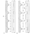
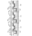
隔壁の底部及び頂部のエッジが丸みを帯びていない例を、図22(B)に示す。図22(B)に示す半導体装置は、角張った形状を有する隔壁1051a及び1051b、その間に開口部1052を有している。また隔壁1051a及び1051bの端部はそれぞれテーパー角φを有している。このような形状では、上記のように水分が侵入する可能性や、ショートを起こしてしまう可能性がある。
An example in which the edges of the bottom and top of the partition are not rounded is illustrated in FIG. A semiconductor device illustrated in FIG. 22B includes
本発明は、樹脂材料から隔壁を形成する際に、ナノインプリント法を用い、断面テーパー角が20°以上50°以下であり、かつ底部及び頂部のエッジ(縁)が丸みを帯びている形状、すなわち曲面を有する形状の隔壁を再現性よく作製することを特徴とする。 The present invention uses a nanoimprint method when forming a partition wall from a resin material, has a cross-section taper angle of 20 ° to 50 °, and has a round shape at the bottom and top edges (edges), that is, A partition wall having a curved surface is manufactured with high reproducibility.
本発明の素子を区切る隔壁は、例えば以下のようにして形成される。 The partition which divides the element of this invention is formed as follows, for example.
素子が形成された基板上に樹脂材料を均一に成膜し、熱インプリント法や光インプリント法で、樹脂材料に鋳型(モールドともいう)を押しつける(押圧する)。次いでモールドを剥離し、必要であれば、残った樹脂材料を酸素プラズマ等で除去する。次いで必要ならば所定の形状に成形された樹脂材料を、加熱や光照射等によって完全に硬化する。以上により隔壁が形成される。 A resin material is uniformly formed on the substrate on which the element is formed, and a mold (also referred to as a mold) is pressed (pressed) against the resin material by a thermal imprint method or an optical imprint method. Next, the mold is peeled off, and if necessary, the remaining resin material is removed with oxygen plasma or the like. Next, if necessary, the resin material molded into a predetermined shape is completely cured by heating, light irradiation, or the like. A partition is formed by the above.
ナノインプリント法を用いて隔壁を形成すると、ステッパ装置を用いる方法と同じ程度の精度、すなわちナノメーター(nm)の精度で隔壁を形成することが可能となる。またナノインプリント法では、モールド(鋳型)を用いて隔壁を形成するため、複数の隔壁を再現性よく形成することができ、バラツキが少なく、作製コストも低くすることが可能である。 When the barrier ribs are formed using the nanoimprint method, the barrier ribs can be formed with the same accuracy as the method using the stepper device, that is, the accuracy of nanometers (nm). In the nanoimprint method, a partition is formed by using a mold, so that a plurality of partitions can be formed with good reproducibility, and there is little variation and the manufacturing cost can be reduced.
本発明は、基板上に、第1の電極を形成し、前記基板及び前記第1の電極上に、熱可塑型樹脂材料または熱硬化型樹脂材料を含む絶縁層を形成し、前記絶縁層にモールドを押圧し、前記第1の電極上の前記絶縁層中に開口部を形成し、前記開口部の形成された絶縁層から、前記モールドを取り外し、前記モールドを取り外した後、前記開口部の形成された絶縁層を硬化させて隔壁を形成し、前記第1の電極及び前記隔壁上に、発光層を形成し、前記発光層上に、第2の電極を形成することを特徴とする半導体装置の作製方法に関するものである。 In the present invention, a first electrode is formed on a substrate, an insulating layer containing a thermoplastic resin material or a thermosetting resin material is formed on the substrate and the first electrode, and the insulating layer is formed on the insulating layer. The mold is pressed, an opening is formed in the insulating layer on the first electrode, the mold is removed from the insulating layer in which the opening is formed, the mold is removed, and then the opening is formed. The insulating layer formed is hardened to form a partition, a light emitting layer is formed on the first electrode and the partition, and a second electrode is formed on the light emitting layer The present invention relates to a method for manufacturing a device.
本発明において、前記絶縁層は、加熱によって硬化されるものである。 In the present invention, the insulating layer is cured by heating.
本発明は、基板上に、第1の電極を形成し、前記基板及び前記第1の電極上に、光硬化型樹脂材料を含む絶縁層を形成し、前記絶縁層にモールドを押圧し、前記第1の電極上の前記絶縁層中に開口部を形成し、前記開口部の形成された絶縁層から、前記モールドを取り外し、前記開口部の形成された絶縁層を硬化させて隔壁を形成し、前記第1の電極及び前記隔壁上に、発光層を形成し、前記発光層上に、第2の電極を形成することを特徴とする半導体装置の作製方法に関するものである。 In the present invention, a first electrode is formed on a substrate, an insulating layer containing a photocurable resin material is formed on the substrate and the first electrode, a mold is pressed against the insulating layer, An opening is formed in the insulating layer on the first electrode, the mold is removed from the insulating layer in which the opening is formed, and a partition is formed by curing the insulating layer in which the opening is formed. The present invention relates to a method for manufacturing a semiconductor device, wherein a light emitting layer is formed over the first electrode and the partition, and a second electrode is formed over the light emitting layer.
本発明において、前記絶縁層は、光照射によって硬化されるものである。 In the present invention, the insulating layer is cured by light irradiation.
本発明において、前記モールドは、金属材料または絶縁材料により形成されており、前記モールドの表面には凹凸が形成されているものを用いる。 In the present invention, the mold is formed of a metal material or an insulating material, and a mold having irregularities formed on the surface of the mold is used.
本発明において、前記隔壁は、断面テーパー角が20°以上50°以下であり、かつ前記隔壁の底部及び頂部のエッジが曲面を有する形状を有しているものを用いる。 In the present invention, the partition wall has a cross-sectional taper angle of 20 ° or more and 50 ° or less, and has a shape in which the bottom and top edges of the partition wall have curved surfaces.
なお本明細書において、半導体装置とは、半導体を利用することで機能する素子及び装置全般を指し、半導体素子を含む発光装置等を含む電気光学装置およびその電気光学装置を搭載した電子機器をその範疇とする。 Note that in this specification, a semiconductor device refers to all elements and devices that function by using a semiconductor, and includes an electro-optical device including a light-emitting device including a semiconductor element and an electronic device including the electro-optical device. Category.
本発明により、樹脂材料を用いた隔壁が簡便な方法で再現性よく作製できる。これにより、バラツキが少なく、コストの低い発光表示装置を作製することができる。 According to the present invention, a partition wall using a resin material can be manufactured with a simple method and good reproducibility. Thus, a light-emitting display device with low variation and low cost can be manufactured.
また隔壁のテーパー角が20°〜50°と大きすぎないため、隔壁上に形成される膜の膜厚が薄くなることを防ぐことができる。そのため隔壁上の膜の物理強度が小さくなることを回避できる。 In addition, since the taper angle of the partition wall is not so large as 20 ° to 50 °, it is possible to prevent the film formed on the partition wall from being thinned. Therefore, it can be avoided that the physical strength of the film on the partition wall is reduced.
また隔壁の底部及び頂部のエッジが丸みを帯びることで、すなわち隔壁の底部及び頂部のエッジが曲面を有する形状を有することで、隔壁上に形成される膜の断裂を防ぐことができる。 In addition, since the bottom and top edges of the partition walls are rounded, that is, the bottom and top edges of the partition walls have a curved surface, the film formed on the partition walls can be prevented from being broken.
隔壁のテーパー角が20°以上50°以下であること、隔壁の底部及び頂部のエッジが丸みを帯びることにより、水分の侵入を防ぎ、またショートを回避することが可能となる。以上により、信頼性の高い発光表示装置を得ることが可能となる。 When the taper angle of the partition is 20 ° or more and 50 ° or less, and the bottom and top edges of the partition are rounded, it is possible to prevent moisture from entering and avoid short circuit. Thus, a highly reliable light-emitting display device can be obtained.
以下、本発明の実施の態様について、図面を参照して説明する。但し、本発明は多くの異なる態様で実施することが可能であり、本発明の趣旨及びその範囲から逸脱することなくその形態及び詳細を様々に変更し得ることは当業者であれば容易に理解される。従って、本実施の形態の記載内容に限定して解釈されるものではない。なお、以下に示す図面において、同一部分又は同様な機能を有する部分には同一の符号を付し、その繰り返しの説明は省略する。 Hereinafter, embodiments of the present invention will be described with reference to the drawings. However, the present invention can be implemented in many different modes, and those skilled in the art can easily understand that the modes and details can be variously changed without departing from the spirit and scope of the present invention. Is done. Therefore, the present invention is not construed as being limited to the description of this embodiment mode. Note that in the drawings described below, the same portions or portions having similar functions are denoted by the same reference numerals, and repetitive description thereof is omitted.
本実施の形態では、本発明を用いて発光表示装置の発光素子を作製する工程について、図1(A)〜図1(B)、図2(A)〜図2(B)、図3(A)〜図3(C)を用いて説明する。 In this embodiment mode, a process for manufacturing a light-emitting element of a light-emitting display device using the present invention will be described with reference to FIGS. 1A to 1B, FIGS. 2A to 2B, and FIG. A) to FIG. 3C will be described.
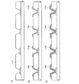
まず、基板101上に第1の電極102(102a、102b、102c、102d、等)を形成する(図1(A)参照)。基板101としては、例えば、ガラス、石英などを用いることができる。なお第1の電極102を形成する前に、基板101上に下地絶縁膜を形成してもよい。
First, the first electrode 102 (102a, 102b, 102c, 102d, or the like) is formed over the substrate 101 (see FIG. 1A). As the
第1の電極102及び後の工程で形成される第2の電極114(114a、114b、114c、114d、等)は、金属、合金、導電性化合物、及びこれらの混合物などを用いることができる。具体的には、例えば、酸化インジウム−酸化スズ(Indium Tin Oxide(「ITO」ともいう))、珪素若しくは酸化珪素を含有した酸化インジウム−酸化スズ、酸化インジウム−酸化亜鉛(Indium Zinc Oxide(「IZO」ともいう))、酸化タングステン及び酸化亜鉛を含む酸化タングステン−酸化インジウム等が挙げられる。これらの導電性金属酸化物膜は、通常スパッタリングにより成膜される。例えば、酸化インジウム−酸化亜鉛(IZO)は、酸化インジウムに対し1〜20wt%の酸化亜鉛を加えたターゲットを用いたスパッタリングにより形成することができる。また、酸化亜鉛を含む酸化タングステン−酸化インジウムは、酸化インジウムに対し酸化タングステンを0.5〜5wt%、酸化亜鉛を0.1〜1wt%含有したターゲットを用いたスパッタリングにより形成することができる。 For the first electrode 102 and the second electrode 114 (114a, 114b, 114c, 114d, and the like) formed in a later step, a metal, an alloy, a conductive compound, a mixture thereof, or the like can be used. Specifically, for example, indium tin oxide (also referred to as “ITO”), indium oxide-tin oxide containing silicon or silicon oxide, indium zinc oxide (“IZO”). And tungsten oxide-indium oxide containing tungsten oxide and zinc oxide. These conductive metal oxide films are usually formed by sputtering. For example, indium oxide-zinc oxide (IZO) can be formed by sputtering using a target in which 1 to 20 wt% of zinc oxide is added to indium oxide. Further, tungsten oxide-indium oxide containing zinc oxide can be formed by sputtering using a target containing 0.5 to 5 wt% tungsten oxide and 0.1 to 1 wt% zinc oxide with respect to indium oxide.
また第1の電極102及び第2の電極114として、上記以外にも、アルミニウム(Al)、銀(Ag)、金(Au)、白金(Pt)、ニッケル(Ni)、タングステン(W)、クロム(Cr)、モリブデン(Mo)、鉄(Fe)、コバルト(Co)、銅(Cu)、パラジウム(Pd)、又は金属材料の窒化物(例えば、窒化チタン)等用いることができる。 In addition to the above, as the first electrode 102 and the second electrode 114, aluminum (Al), silver (Ag), gold (Au), platinum (Pt), nickel (Ni), tungsten (W), chromium (Cr), molybdenum (Mo), iron (Fe), cobalt (Co), copper (Cu), palladium (Pd), or a nitride of a metal material (for example, titanium nitride) can be used.
なお、第1の電極102及び第2の電極114、あるいは第1の電極102及び第2の電極114のどちらか一方を、透光性を有する電極とする場合、可視光の透過率の低い材料であっても、1nm〜50nm、好ましくは5nm〜20nm程度の厚さで成膜することで、透光性の電極として用いることができる。なお、スパッタリング以外にも、真空蒸着法、CVD法、ゾル−ゲル法を用いて電極を作製することもできる。 Note that in the case where any one of the first electrode 102 and the second electrode 114 or the first electrode 102 and the second electrode 114 is a light-transmitting electrode, the material has low visible light transmittance. Even so, it can be used as a light-transmitting electrode by forming a film with a thickness of about 1 nm to 50 nm, preferably about 5 nm to 20 nm. In addition to sputtering, an electrode can also be produced using a vacuum deposition method, a CVD method, or a sol-gel method.
ただし、発光は、第1の電極102もしくは第2の電極114を通って外部に取り出されるため、第1の電極102および第2の電極114のうち、少なくとも一方は透光性を有する材料で形成されている必要がある。また、第2の電極114よりも第1の電極102における仕事関数が大きくなるように材料を選択することが好ましい。さらに第1の電極102と第2の電極114はそれぞれ一層である必要は無く、2層以上の構成を取っていても良い。 However, since light emission is extracted to the outside through the first electrode 102 or the second electrode 114, at least one of the first electrode 102 and the second electrode 114 is formed using a light-transmitting material. Need to be. The material is preferably selected so that the work function of the first electrode 102 is higher than that of the second electrode 114. Further, the first electrode 102 and the second electrode 114 do not have to be one layer each, and may have a structure of two or more layers.
そして図1(B)に示すように、基板101及び第1の電極102上に、樹脂材料からなる絶縁層104を形成する。絶縁層104は、熱可塑型樹脂材料や光硬化型樹脂材料を含む絶縁層を用いればよい。
Then, as illustrated in FIG. 1B, an insulating
このような熱可塑型樹脂材料や光硬化型樹脂材料としては、次のような材料を用いればよい。すなわち、アクリル、ノボラック樹脂、珪素を含む樹脂、ジアリルフタレート樹脂、塩化ビニル樹脂、酢酸ビニル樹脂、ポリビニルアルコール、ポリスチレン、メタクリル樹脂、ポリエチレン樹脂、ポリプロピレン、ポリカーボネート、ポリエステル、ポリアミド(ナイロン)等である。 As such a thermoplastic resin material or a photocurable resin material, the following materials may be used. That is, acrylic, novolac resin, silicon-containing resin, diallyl phthalate resin, vinyl chloride resin, vinyl acetate resin, polyvinyl alcohol, polystyrene, methacrylic resin, polyethylene resin, polypropylene, polycarbonate, polyester, polyamide (nylon) and the like.
また、ポリイミド、フェノール樹脂、メラミン樹脂、エポキシ樹脂等の熱硬化型樹脂も用いることが可能である。 Moreover, thermosetting resins such as polyimide, phenol resin, melamine resin, and epoxy resin can also be used.
次いで絶縁層104に、鋳型(モールドともいう)105を押しつけて、絶縁層104に開口部107(107a、107b、107c、107d等)を形成する(図2(A)参照)。例えば、絶縁層104として熱可塑性樹脂材料を用いる場合は、絶縁層104をガラス転移点よりも高い温度で加熱し、柔らかくなった状態でモールド105を押しつけ、温度が低くなって絶縁層104が再び硬くなった状態でモールドを離す。絶縁層104として光硬化型樹脂材料を用いる場合は、モールド105を押しつけた後、光照射(代表的には紫外線照射)を行うことにより絶縁層104を硬化させる。
Next, a mold (also referred to as a mold) 105 is pressed against the insulating
また絶縁層104として、熱硬化型樹脂材料を用いる場合は、絶縁層104にモールド105を押圧しながら、すなわち押しつけながら硬化温度まで加熱、そのままモールド105を保持して硬化させる。
When a thermosetting resin material is used as the insulating
モールド105は、金属材料や、石英などの絶縁材料によって形成されており、あらかじめ表面に凹凸が形成されている。表面の凹凸は、例えば電子線描画を用いて形成される。
The
このとき、後の工程で完成される隔壁112の断面テーパー角が20°〜50°を有し、かつ隔壁112の底部及び頂部のエッジ(縁)が丸みを帯びる形状、すなわち曲面を有する形状になるように、モールド105表面の凹凸を形成する。このようなテーパー角及び形状を持つ隔壁112を形成すると、隔壁112上に発光層113及び第2の電極114を形成したときに、ステップカバレッジがよくなり、ショートを防ぐことができるという利点がある。
At this time, the cross-sectional taper angle of the
図22(A)に、本発明の隔壁の底部及び頂部のエッジが丸みを帯びている半導体装置を示す。図22(A)の隔壁151(151a及び151b)は、図3(A)の隔壁112と同じものである。図22(A)では、底部及び頂部のエッジが丸みを帯びている隔壁151a及び151b、その間に開口部152を有している。また隔壁151の端部はテーパー角θを有している。このような形状を有する隔壁では、隔壁151a及び151b上、並びに開口部152に形成される膜(発光層113等)の断裂を防ぐことができるので、結果としてショートが起きるのを防ぐことが可能となる。
FIG. 22A shows a semiconductor device in which the bottom and top edges of the partition wall of the present invention are rounded. A partition wall 151 (151a and 151b) in FIG. 22A is the same as the
次に図2(B)に示すように、モールド105を絶縁層104から取り外す。このとき絶縁層104に超音波を用いて振動を加えることで、絶縁層104の変形を抑えながら、モールド105を絶縁層104から取り外すことができる。モールド105を取り外すことで、パターンが形成された絶縁層109を形成することができる。
Next, as shown in FIG. 2B, the
またこのとき、もし必要であればウェットエッチングやドライエッチングにより、電極102上に樹脂材料の残滓を除去する。例えば酸素プラズマ等で電極102上に残った樹脂材料を除去すればよい。 At this time, the residue of the resin material on the electrode 102 is removed by wet etching or dry etching if necessary. For example, the resin material remaining on the electrode 102 may be removed by oxygen plasma or the like.
次いで絶縁層109を加熱し、絶縁層109を完全に硬化させ、隔壁112とする(図3(A)参照)。硬化の方法は、樹脂により加熱処理もしくは光照射等を行って硬化させればよい。
Next, the insulating
次に、第1の電極102及び隔壁112上に発光層113(113a、113b、113c、113d、等)を形成する(図3(B)参照)。本実施の形態では、発光層113として、有機化合物を用いる。 Next, a light-emitting layer 113 (113a, 113b, 113c, 113d, and the like) is formed over the first electrode 102 and the partition 112 (see FIG. 3B). In this embodiment mode, an organic compound is used for the light-emitting layer 113.
有機化合物の発光層113としては、次のような材料を用いることができる。例えば、赤色の発光を示す発光材料として、Alq3(トリス(8−キノリノラト)アルミニウム):DCM1(4−(ジシアノメチレン)−2−メチル−6−(p−ジメチルアミノスチリル)−4H−ピラン)、またはAlq3:ルブレン:BisDCJTMなどの材料を用いる。また、緑色の発光を示す発光材料としては、Alq3:DMQD(N,N’−ジメチルキナクリドン)、またはAlq3:クマリン6などの材料を用いる。また、青色の発光を示す発光材料としては、α−NPD、またはtBu−DNAなどの材料を用いる。 For the organic compound light-emitting layer 113, the following materials can be used. For example, as a light-emitting material that emits red light, Alq 3 (tris (8-quinolinolato) aluminum): DCM1 (4- (dicyanomethylene) -2-methyl-6- (p-dimethylaminostyryl) -4H-pyran) Alternatively, a material such as Alq 3 : rubrene: BisDCJTM is used. As a light-emitting material that emits green light, a material such as Alq 3 : DMQD (N, N′-dimethylquinacridone) or Alq 3 : coumarin 6 is used. As a light-emitting material that emits blue light, a material such as α-NPD or tBu-DNA is used.
また発光層113として、無機化合物を用いる場合においても、本発明は適用することが可能である。 The present invention can also be applied to the case where an inorganic compound is used as the light emitting layer 113.
無機化合物を発光材料として用いる無機EL素子は、その素子構成により、分散型無機EL素子と薄膜型無機EL素子とに分類される。前者は、発光材料の粒子をバインダ中に分散させた電界発光層を有し、後者は、発光材料の薄膜からなる電界発光層を有している点に違いはあるが、高電界で加速された電子を必要とする点では共通である。なお、得られる発光のメカニズムとしては、ドナー準位とアクセプター準位を利用するドナー−アクセプター再結合型発光と、金属イオンの内殻電子遷移を利用する局在型発光とがある。一般的に、分散型無機EL素子ではドナー−アクセプター再結合型発光、薄膜型無機EL素子では局在型発光である場合が多い。 Inorganic EL elements using an inorganic compound as a light emitting material are classified into a dispersion type inorganic EL element and a thin film type inorganic EL element depending on the element structure. The former has an electroluminescent layer in which particles of a luminescent material are dispersed in a binder, and the latter has an electroluminescent layer made of a thin film of luminescent material, but is accelerated by a high electric field. This is common in that it requires more electrons. Note that the obtained light emission mechanism includes donor-acceptor recombination light emission using a donor level and an acceptor level, and localized light emission using inner-shell electron transition of a metal ion. In general, the dispersion-type inorganic EL element often has donor-acceptor recombination light emission, and the thin-film inorganic EL element often has localized light emission.
本発明で用いることのできる発光材料は、母体材料と発光中心となる不純物元素とで構成される。含有させる不純物元素を変化させることで、様々な色の発光を得ることができる。発光材料の作製方法としては、固相法や液相法(共沈法)などの様々な方法を用いることができる。また、噴霧熱分解法、複分解法、プレカーサーの熱分解反応による方法、逆ミセル法やこれらの方法と高温焼成を組み合わせた方法、凍結乾燥法などの液相法なども用いることができる。 A light-emitting material that can be used in the present invention includes a base material and an impurity element serving as a light emission center. By changing the impurity element to be contained, light emission of various colors can be obtained. As a method for manufacturing the light-emitting material, various methods such as a solid phase method and a liquid phase method (coprecipitation method) can be used. Also, spray pyrolysis method, metathesis method, precursor thermal decomposition method, reverse micelle method, method combining these methods with high temperature firing, liquid phase method such as freeze-drying method, etc. can be used.
固相法は、母体材料と、不純物元素又は不純物元素を含む化合物を秤量し、乳鉢で混合、電気炉で加熱、焼成を行い反応させ、母体材料に不純物元素を含有させる方法である。焼成温度は、700〜1500℃が好ましい。温度が低すぎる場合は固相反応が進まず、温度が高すぎる場合は母体材料が分解してしまうからである。なお、粉末状態で焼成を行ってもよいが、ペレット状態で焼成を行うことが好ましい。比較的高温での焼成を必要とするが、簡単な方法であるため、生産性がよく大量生産に適している。 The solid phase method is a method in which a base material and an impurity element or a compound containing the impurity element are weighed, mixed in a mortar, heated and fired in an electric furnace, reacted, and the base material contains the impurity element. The firing temperature is preferably 700 to 1500 ° C. This is because the solid phase reaction does not proceed when the temperature is too low, and the base material is decomposed when the temperature is too high. In addition, although baking may be performed in a powder state, it is preferable to perform baking in a pellet state. Although firing at a relatively high temperature is required, it is a simple method, so it has high productivity and is suitable for mass production.
液相法(共沈法)は、母体材料又は母体材料を含む化合物と、不純物元素又は不純物元素を含む化合物を溶液中で反応させ、乾燥させた後、焼成を行う方法である。発光材料の粒子が均一に分布し、粒径が小さく低い焼成温度でも反応が進むことができる。 The liquid phase method (coprecipitation method) is a method in which a base material or a compound containing the base material and an impurity element or a compound containing the impurity element are reacted in a solution, dried, and then fired. The particles of the luminescent material are uniformly distributed, and the reaction can proceed even at a low firing temperature with a small particle size.
発光材料に用いる母体材料としては、硫化物、酸化物、窒化物を用いることができる。硫化物としては、例えば、硫化亜鉛(ZnS)、硫化カドミウム(CdS)、硫化カルシウム(CaS)、硫化イットリウム(Y2S3)、硫化ガリウム(Ga2S3)、硫化ストロンチウム(SrS)、硫化バリウム(BaS)等を用いることができる。また、酸化物としては、例えば、酸化亜鉛(ZnO)、酸化イットリウム(Y2O3)等を用いることができる。また、窒化物としては、例えば、窒化アルミニウム(AlN)、窒化ガリウム(GaN)、窒化インジウム(InN)等を用いることができる。さらに、セレン化亜鉛(ZnSe)、テルル化亜鉛(ZnTe)等も用いることができ、硫化カルシウム−ガリウム(CaGa2S4)、硫化ストロンチウム−ガリウム(SrGa2S4)、硫化バリウム−ガリウム(BaGa2S4)、等の3元系の混晶であってもよい。 As a base material used for the light-emitting material, sulfide, oxide, or nitride can be used. Examples of the sulfide include zinc sulfide (ZnS), cadmium sulfide (CdS), calcium sulfide (CaS), yttrium sulfide (Y 2 S 3 ), gallium sulfide (Ga 2 S 3 ), strontium sulfide (SrS), sulfide. Barium (BaS) or the like can be used. As the oxide, for example, zinc oxide (ZnO), yttrium oxide (Y 2 O 3 ), or the like can be used. As the nitride, for example, aluminum nitride (AlN), gallium nitride (GaN), indium nitride (InN), or the like can be used. Furthermore, zinc selenide (ZnSe), zinc telluride (ZnTe), and the like can also be used, and calcium sulfide-gallium sulfide (CaGa 2 S 4 ), strontium sulfide-gallium sulfide (SrGa 2 S 4 ), barium sulfide-gallium (BaGa). It may be a ternary mixed crystal such as 2 S 4 ).
局在型発光の発光中心として、マンガン(Mn)、銅(Cu)、サマリウム(Sm)、テルビウム(Tb)、エルビウム(Er)、ツリウム(Tm)、ユーロピウム(Eu)、セリウム(Ce)、プラセオジウム(Pr)などを用いることができる。なお、電荷補償として、フッ素(F)、塩素(Cl)などのハロゲン元素が添加されていてもよい。 As emission centers of localized emission, manganese (Mn), copper (Cu), samarium (Sm), terbium (Tb), erbium (Er), thulium (Tm), europium (Eu), cerium (Ce), praseodymium (Pr) or the like can be used. Note that a halogen element such as fluorine (F) or chlorine (Cl) may be added as charge compensation.
一方、ドナー−アクセプター再結合型発光の発光中心として、ドナー準位を形成する第1の不純物元素及びアクセプター準位を形成する第2の不純物元素を含む発光材料を用いることができる。第1の不純物元素は、例えば、フッ素(F)、塩素(Cl)、アルミニウム(Al)等を用いることができる。第2の不純物元素としては、例えば、銅(Cu)、銀(Ag)等を用いることができる。 On the other hand, a light-emitting material containing a first impurity element that forms a donor level and a second impurity element that forms an acceptor level can be used as the emission center of donor-acceptor recombination light emission. As the first impurity element, for example, fluorine (F), chlorine (Cl), aluminum (Al), or the like can be used. For example, copper (Cu), silver (Ag), or the like can be used as the second impurity element.
ドナー−アクセプター再結合型発光の発光材料を固相法を用いて合成する場合、母体材料と、第1の不純物元素又は第1の不純物元素を含む化合物と、第2の不純物元素又は第2の不純物元素を含む化合物をそれぞれ秤量し、乳鉢で混合した後、電気炉で加熱、焼成を行う。母体材料としては、上述した母体材料を用いることができ、第1の不純物元素又は第1の不純物元素を含む化合物としては、例えば、フッ素(F)、塩素(Cl)、硫化アルミニウム(Al2S3)等を用いることができ、第2の不純物元素又は第2の不純物元素を含む化合物としては、例えば、銅(Cu)、銀(Ag)、硫化銅(Cu2S)、硫化銀(Ag2S)等を用いることができる。焼成温度は、700〜1500℃が好ましい。温度が低すぎる場合は固相反応が進まず、温度が高すぎる場合は母体材料が分解してしまうからである。なお、粉末状態で焼成を行ってもよいが、ペレット状態で焼成を行うことが好ましい。 In the case where a light-emitting material for donor-acceptor recombination light emission is synthesized using a solid-phase method, a base material, a first impurity element or a compound containing the first impurity element, a second impurity element, or a second impurity element Each compound containing an impurity element is weighed and mixed in a mortar, and then heated and fired in an electric furnace. As the base material, the above-described base material can be used, and examples of the first impurity element or the compound containing the first impurity element include fluorine (F), chlorine (Cl), and aluminum sulfide (Al 2 S). 3 ) or the like, and examples of the second impurity element or the compound containing the second impurity element include copper (Cu), silver (Ag), copper sulfide (Cu 2 S), and silver sulfide (Ag). 2 S) or the like can be used. The firing temperature is preferably 700 to 1500 ° C. This is because the solid phase reaction does not proceed when the temperature is too low, and the base material is decomposed when the temperature is too high. In addition, although baking may be performed in a powder state, it is preferable to perform baking in a pellet state.
また、固相反応を利用する場合の不純物元素として、第1の不純物元素と第2の不純物元素で構成される化合物を組み合わせて用いてもよい。この場合、不純物元素が拡散されやすく、固相反応が進みやすくなるため、均一な発光材料を得ることができる。さらに、余分な不純物元素が入らないため、純度の高い発光材料が得ることができる。第1の不純物元素と第2の不純物元素で構成される化合物としては、例えば、塩化銅(CuCl)、塩化銀(AgCl)等を用いることができる。 In addition, as an impurity element in the case of using a solid phase reaction, a compound including a first impurity element and a second impurity element may be used in combination. In this case, since the impurity element is easily diffused and the solid-phase reaction easily proceeds, a uniform light emitting material can be obtained. Further, since no extra impurity element is contained, a light-emitting material with high purity can be obtained. As the compound including the first impurity element and the second impurity element, for example, copper chloride (CuCl), silver chloride (AgCl), or the like can be used.
なお、これらの不純物元素の濃度は、母体材料に対して0.01〜10atom%であればよく、好ましくは0.05〜5atom%の範囲である。 Note that the concentration of these impurity elements may be 0.01 to 10 atom% with respect to the base material, and is preferably in the range of 0.05 to 5 atom%.
薄膜型無機ELの場合、発光層は、上記発光材料を含む層であり、抵抗加熱蒸着法、電子ビーム蒸着(EB蒸着)法等の真空蒸着法、スパッタリング法等の物理気相成長法(PVD)、有機金属CVD法、ハイドライド輸送減圧CVD法等の化学気相成長法(CVD)、原子層エピタキシ法(ALE)等を用いて形成することができる。 In the case of a thin-film inorganic EL, the light emitting layer is a layer containing the above light emitting material, and a physical vapor deposition method (PVD) such as a resistance heating vapor deposition method, a vacuum vapor deposition method such as an electron beam vapor deposition (EB vapor deposition) method, or a sputtering method. ), Chemical vapor deposition (CVD) such as organometallic CVD, hydride transport low pressure CVD, and atomic layer epitaxy (ALE).
次いで発光層113上に、第2の電極114(114a、114b、114c、114d、等)を形成する(図3(C)参照)。第2の電極114の材料及び作製工程は、第1の電極102の作製の際に示したとおりである。 Next, second electrodes 114 (114a, 114b, 114c, 114d, and the like) are formed over the light-emitting layer 113 (see FIG. 3C). The material and manufacturing process of the second electrode 114 are as described in manufacturing the first electrode 102.
本実施の形態により、樹脂材料を用いた隔壁が簡便な方法で再現性よく作製できる。これにより、バラツキが少なく、コストの低い発光表示装置を作製することができる。また隔壁のテーパー角が20°〜50°と大きすぎないため、隔壁上に形成される膜の膜厚が薄くなることを防ぐことができる。そのため隔壁上の膜の物理強度が小さくなることを回避できる。 According to this embodiment mode, a partition wall using a resin material can be manufactured with a simple method with good reproducibility. Thus, a light-emitting display device with low variation and low cost can be manufactured. In addition, since the taper angle of the partition wall is not so large as 20 ° to 50 °, it is possible to prevent the film formed on the partition wall from being thinned. Therefore, it can be avoided that the physical strength of the film on the partition wall is reduced.
なお本実施の形態は、必要であれば実施例とも組み合わせることが可能である。 Note that this embodiment mode can be combined with any of the examples if necessary.
本発明を用いて半導体装置を作製する方法を、図4(A)〜図4(D)、図5(A)〜図5(C)、図6(A)〜図6(C)、図7(A)〜図7(B)及び図8(A)〜図8(B)、図9(A)〜図9(B)、図10、図11、図12を用いて説明する。 4A to 4D, FIGS. 5A to 5C, FIGS. 6A to 6C, and FIGS. 6A to 6C are diagrams illustrating a method for manufacturing a semiconductor device using the present invention. 7 (A) to FIG. 7 (B) and FIGS. 8 (A) to 8 (B), FIG. 9 (A) to FIG. 9 (B), FIG. 10, FIG. 11, and FIG.
まず図4(A)に示すように、基板501上に下地膜502を成膜する。基板501には、例えばバリウムホウケイ酸ガラスや、アルミノホウケイ酸ガラスなどのガラス基板、石英基板、ステンレス基板等を用いることができる。また、PET(ポリエチレンテレフタレート)、PES(ポリエーテルサルフォン)、PEN(ポリエチレンナフタレート)に代表されるプラスチックや、アクリル等の可撓性を有する合成樹脂からなる基板を用いることも可能である。
First, as shown in FIG. 4A, a
下地膜502は基板501中に含まれるNaなどのアルカリ金属やアルカリ土類金属が、半導体膜中に拡散し、半導体素子の特性に悪影響を及ぼすのを防ぐために設ける。
The
下地膜502としては、酸化珪素、窒化珪素、窒素を含む酸化珪素、酸素を含む窒化珪素などを用いることができ、単層でも2層、3層といった積層構造でもよい。またガラス基板、ステンレス基板またはプラスチック基板のように、アルカリ金属やアルカリ土類金属が多少なりとも含まれている基板を用いる場合、不純物の拡散を防ぐという観点から下地膜を設けることは有効であるが、石英基板など不純物の拡散がさして問題とならない場合は、必ずしも設ける必要はない。
As the
本実施例では、基板上にSiH4、NH3、N2O、N2及びH2を反応ガスとして酸素を含む窒化珪素膜を下層下地膜502aとして膜厚50nm形成し、その上にSiH4及びN2Oを反応ガスとして窒素を含む酸化珪素膜を上層下地膜502bとして膜厚100nmで形成する。また酸素を含む窒化珪素膜の膜厚を140nm、積層する窒素を含む酸化珪素膜の膜厚を100nmとしてもよい。
In this embodiment, a silicon nitride film containing oxygen is formed as a
次に下地膜502上に半導体膜503を形成する。半導体膜503の膜厚は25nm〜100nm(好ましくは30nm〜60nm)とする。なお半導体はシリコン(Si)だけではなくシリコンゲルマニウム(SiGe)も用いることができる。シリコンゲルマニウムを用いる場合、ゲルマニウムの濃度は0.01〜4.5atomic%程度であることが好ましい。
Next, a
半導体膜503は、シランやゲルマン等の半導体材料ガスを用いて気相成長法やスパッタリング法で作製される非晶質半導体(以下「アモルファス半導体」ともいう)、あるいはセミアモルファス半導体(微結晶若しくはマイクロクリスタルとも呼ばれる。以下「SAS」ともいう)などを用いることができる。
The
セミアモルファス半導体(SAS)は、非晶質と結晶構造(単結晶、多結晶を含む)の中間的な構造を有し、自由エネルギー的に安定な第3の状態を有する半導体であって、短距離秩序を持ち格子歪みを有する結晶質な領域を含んでいる。少なくとも膜中の一部の領域には、0.5〜20nmの結晶領域を観測することができ、珪素を主成分とする場合にはラマンスペクトルが520cm−1よりも低波数側にシフトしている。 A semi-amorphous semiconductor (SAS) is a semiconductor having an intermediate structure between amorphous and crystalline structures (including single crystal and polycrystal) and having a third state that is stable in terms of free energy, It includes a crystalline region with distance order and lattice distortion. A crystal region of 0.5 to 20 nm can be observed in at least a part of the film, and when silicon is a main component, the Raman spectrum is shifted to a lower wave number side than 520 cm −1. Yes.
X線回折では珪素結晶格子に由来するとされる(111)、(220)の回折ピークが観測される。未結合手(ダングリングボンド)の終端化させるものとして水素またはハロゲンを少なくとも1原子%またはそれ以上含ませている。 In X-ray diffraction, diffraction peaks of (111) and (220) that are derived from the silicon crystal lattice are observed. Hydrogen or halogen is contained at least 1 atomic% or more as a terminal for dangling bonds (dangling bonds).
SASは、珪素を含む気体をグロー放電分解(プラズマCVD)して形成する。珪素を含む気体としては、SiH4、その他にもSi2H6、SiH2Cl2、SiHCl3、SiCl4、SiF4などを用いることが可能である。またF2、GeF4を混合させても良い。この珪素を含む気体をH2、又は、H2とHe、Ar、Kr、Neから選ばれた一種または複数種の希ガス元素で希釈しても良い。 SAS is formed by glow discharge decomposition (plasma CVD) of a gas containing silicon. As a gas containing silicon, SiH 4 , Si 2 H 6 , SiH 2 Cl 2 , SiHCl 3 , SiCl 4 , SiF 4, or the like can be used. Further, F 2 and GeF 4 may be mixed. The gas containing silicon may be diluted with H 2 , or H 2 and one or more kinds of rare gas elements selected from He, Ar, Kr, and Ne.
希釈率は2〜1000倍の範囲、圧力は0.1Pa〜133Paの範囲、電源周波数は1MHz〜120MHz、好ましくは13MHz〜60MHzである。基板加熱温度は300℃以下が好ましく、100〜200℃の基板加熱温度でも形成可能である。 The dilution rate is in the range of 2 to 1000 times, the pressure is in the range of 0.1 Pa to 133 Pa, and the power supply frequency is 1 MHz to 120 MHz, preferably 13 MHz to 60 MHz. The substrate heating temperature is preferably 300 ° C. or lower, and can be formed even at a substrate heating temperature of 100 to 200 ° C.
ここで、主に成膜時に取り込まれる不純物元素として、酸素、窒素、炭素などの大気成分に由来する不純物は1×1020cm−3以下とすることが望ましく、特に、酸素濃度は5×1019cm−3以下、好ましくは1×1019cm−3以下となるようにすることが好ましい。 Here, as an impurity element mainly taken in at the time of film formation, impurities derived from atmospheric components such as oxygen, nitrogen, and carbon are preferably 1 × 10 20 cm −3 or less, and in particular, the oxygen concentration is 5 × 10 5. It is preferable to be 19 cm −3 or less, preferably 1 × 10 19 cm −3 or less.
また、ヘリウム、アルゴン、クリプトン、ネオンなどの希ガス元素を含ませて格子歪みをさらに助長させることで安定性が増し良好なSASが得られる。また半導体膜としてフッ素系ガスより形成されるSAS層に水素系ガスより形成されるSAS層を積層してもよい。 Further, by adding a rare gas element such as helium, argon, krypton, or neon to further promote lattice distortion, stability is improved and a favorable SAS can be obtained. In addition, a SAS layer formed of a hydrogen-based gas may be stacked on a SAS layer formed of a fluorine-based gas as a semiconductor film.
非晶質半導体としては、代表的には水素化アモルファスシリコンなどがあげられる。また前述したように、セミアモルファス半導体又は半導体膜の一部に結晶相を含む半導体を用いることもできる。 A typical example of the amorphous semiconductor is hydrogenated amorphous silicon. Further, as described above, a semi-amorphous semiconductor or a semiconductor containing a crystal phase in part of a semiconductor film can also be used.
本実施例では、半導体膜503として、プラズマCVD法で非晶質珪素膜を54nmの厚さで成膜する。
In this embodiment, an amorphous silicon film with a thickness of 54 nm is formed as the
次に半導体膜503に半導体の結晶化を促進する金属元素を導入する。半導体膜503への金属元素の導入の方法としては、金属元素を半導体膜503の表面又はその内部に存在させ得る手法であれば特に限定はなく、例えばスパッタ法、CVD法、プラズマ処理法(プラズマCVD法も含む)、吸着法、金属塩の溶液を添加する方法を使用することができる。
Next, a metal element that promotes crystallization of the semiconductor is introduced into the
このうち溶液を用いる方法は簡便であり、金属元素の濃度調整が容易であるという点で有用である。また、このとき半導体膜503の表面のぬれ性を改善し、非晶質半導体膜の表面全体に水溶液を行き渡らせるため、酸素雰囲気中でのUV光の照射、熱酸化法、ヒドロキシラジカルを含むオゾン水又は過酸化水素による処理等により、酸化膜を成膜することが望ましい。
Among these, the method using a solution is simple and useful in that the concentration of the metal element can be easily adjusted. At this time, in order to improve the wettability of the surface of the
半導体の結晶化を促進する金属元素としては、ニッケル(Ni)、ゲルマニウム(Ge)、鉄(Fe)、パラジウム(Pd)、スズ(Sn)、鉛(Pb)、コバルト(Co)、白金(Pt)、銅(Cu)、金(Au)から選ばれた一つの元素、又は複数の元素を用いることが可能である。本実施例では、金属元素としてニッケル(Ni)を用い、金属元素を含む溶液504として液相のニッケル酢酸溶液をスピンコート法で半導体膜503の表面に添加する(図4(A)参照)。
Examples of metal elements that promote semiconductor crystallization include nickel (Ni), germanium (Ge), iron (Fe), palladium (Pd), tin (Sn), lead (Pb), cobalt (Co), and platinum (Pt ), Copper (Cu), gold (Au), or a single element or a plurality of elements. In this embodiment, nickel (Ni) is used as a metal element, and a liquid nickel acetate solution is added to the surface of the
次に窒素雰囲気中において、450〜500℃の温度で1時間保持することにより、半導体膜503中の水素を離脱させる。これは、半導体膜503中に不対結合手を意図的に形成することにより、後の結晶化に際してのしきい値エネルギーを下げるためである。
Next, hydrogen in the
そして窒素雰囲気中において、550〜600℃、4〜8時間の加熱処理を施すことにより、半導体膜503を結晶化させて結晶性半導体膜505を得る。この金属元素により、半導体膜503の結晶化の温度を550〜600℃という比較的低温とすることができる。
Then, by performing heat treatment at 550 to 600 ° C. for 4 to 8 hours in a nitrogen atmosphere, the
次に、結晶性半導体膜505に線状レーザビーム500を照射し、結晶性をさらに改善する(図4(B)参照)。
Next, the
レーザ結晶化を行なう場合、レーザ結晶化の前に、レーザに対する結晶性半導体膜505の耐性を高めるために、500℃、1時間の加熱処理を結晶性半導体膜505に加えてもよい。
In the case of performing laser crystallization, heat treatment for one hour at 500 ° C. may be applied to the
レーザ結晶化は、連続発振のレーザ、または擬似CWレーザとして、発振周波数が10MHz以上、好ましくは80MHz以上のパルス発振レーザを用いることができる。 For laser crystallization, a pulsed laser having an oscillation frequency of 10 MHz or more, preferably 80 MHz or more can be used as a continuous wave laser or a pseudo CW laser.
具体的には、連続発振のレーザとして、Arレーザ、Krレーザ、CO2レーザ、YAGレーザ、YVO4レーザ、YLFレーザ、YAlO3レーザ、GdVO4レーザ、Y2O3レーザ、ルビーレーザ、アレキサンドライトレーザ、Ti:サファイアレーザ、ヘリウムカドミウムレーザなどが挙げられる。 Specifically, as a continuous wave laser, Ar laser, Kr laser, CO 2 laser, YAG laser, YVO 4 laser, YLF laser, YAlO 3 laser, GdVO 4 laser, Y 2 O 3 laser, ruby laser, alexandrite laser Ti: sapphire laser, helium cadmium laser, and the like.
また擬似CWレーザとして、発振周波数が10MHz以上、好ましくは80MHz以上のパルス発振させることができるのであれば、Arレーザ、Krレーザ、エキシマレーザ、CO2レーザ、YAGレーザ、Y2O3レーザ、YVO4レーザ、YLFレーザ、YAlO3レーザ、GdVO4レーザ、ガラスレーザ、ルビーレーザ、アレキサンドライトレーザ、Ti:サファイアレーザ、銅蒸気レーザまたは金蒸気レーザのようなパルス発振レーザを用いることができる。 As a pseudo CW laser, an Ar laser, a Kr laser, an excimer laser, a CO 2 laser, a YAG laser, a Y 2 O 3 laser, a YVO can be used as long as it can oscillate a pulse having an oscillation frequency of 10 MHz or more, preferably 80 MHz or more. A pulsed laser such as a 4 laser, a YLF laser, a YAlO 3 laser, a GdVO 4 laser, a glass laser, a ruby laser, an alexandrite laser, a Ti: sapphire laser, a copper vapor laser, or a gold vapor laser can be used.
このようなパルス発振レーザは、発振周波数を増加させていくと、いずれは連続発振レーザと同等の効果を示すものである。 Such a pulsed laser has an effect equivalent to that of a continuous wave laser as the oscillation frequency is increased.
例えば連続発振が可能な固体レーザを用いる場合、第2高調波〜第4高調波のレーザ光を照射することで、大粒径の結晶を得ることができる。代表的には、YAGレーザ(基本波1064nm)の第2高調波(532nm)や第3高調波(355nm)を用いるのが望ましい。例えば、連続発振のYAGレーザから射出されたレーザ光を非線形光学素子により高調波に変換して、半導体膜505に照射する。エネルギー密度は0.01〜100MW/cm2程度(好ましくは0.1〜10MW/cm2)とすれば良い。
For example, when a solid-state laser capable of continuous oscillation is used, a crystal having a large grain size can be obtained by irradiating laser light of second to fourth harmonics. Typically, it is desirable to use the second harmonic (532 nm) or the third harmonic (355 nm) of a YAG laser (fundamental wave 1064 nm). For example, laser light emitted from a continuous wave YAG laser is converted into a harmonic by a non-linear optical element, and irradiated to the
なお、希ガスや窒素などの不活性ガスを含む雰囲気中でレーザ光を照射するようにしても良い。これにより、レーザ光照射による半導体表面の荒れを抑えることができ、界面準位密度のばらつきによって生じる閾値電圧のばらつきを抑えることができる。 Note that laser light irradiation may be performed in an atmosphere containing an inert gas such as a rare gas or nitrogen. Thereby, roughness of the semiconductor surface due to laser light irradiation can be suppressed, and variation in threshold voltage caused by variation in interface state density can be suppressed.
上述した半導体膜505へのレーザビーム500の照射により、結晶性がより高められた結晶性半導体膜506が形成される(図4(C)参照)。
By irradiation of the
次に、図4(D)に示すように結晶性半導体膜506を用いて、島状半導体膜507、島状半導体膜508、島状半導体膜509、島状半導体膜510が形成される。この島状半導体膜507〜島状半導体膜510は、以降の工程で形成されるTFTの活性層となる。
Next, as illustrated in FIG. 4D, an island-shaped
次に島状半導体膜507〜島状半導体膜510にしきい値制御のための不純物を導入する。本実施例においてはジボラン(B2H6)をドープすることによってボロン(B)を島状半導体膜507〜島状半導体膜510それぞれに導入する。
Next, impurities for threshold control are introduced into the island-shaped
次に島状半導体膜507〜島状半導体膜510を覆うように絶縁膜511を成膜する。絶縁膜511には、例えば酸化珪素、窒化珪素または窒素を含んだ酸化珪素等を用いることができる。また成膜方法は、プラズマCVD法、スパッタ法などを用いることができる。
Next, an insulating
次に、絶縁膜511上に導電膜を成膜した後、第1導電膜512及び第2導電膜513を成膜し、これらを用いてゲート電極515、ゲート電極516、ゲート電極517、ゲート電極518、ゲート電極519を形成する。
Next, after a conductive film is formed over the insulating
ゲート電極515〜ゲート電極519は、導電膜を単層または2層以上積層させた構造を用いて形成する。導電膜を2層以上積層させている場合は、タンタル(Ta)、タングステン(W)、チタン(Ti)、モリブデン(Mo)、アルミニウム(Al)から選ばれた元素、または前記元素を主成分とする合金材料、若しくは化合物材料を積層させてゲート電極515〜ゲート電極519を形成してもよい。また、リン(P)等の不純物元素をドーピングした多結晶シリコン膜に代表される半導体膜を用いてゲート電極を形成してもよい。
The
本実施例では、まず第1の導電膜512として、例えば窒化タンタル膜を10〜50nm、例えば30nmの膜厚で形成する。そして第1の導電膜512上に第2の導電膜513として、例えばタングステン(W)膜を200〜400nm、例えば370nmの膜厚で形成し、第1の導電膜512及び第2の導電膜513の積層膜を形成する(図5(A)参照)。
In this embodiment, first, as the first
次に第2の導電膜と第1の導電膜を連続的に異方性エッチングし、次いで第2の導電膜を等方性エッチングすることで、上層ゲート電極515b〜上層ゲート電極519b、下層ゲート電極515a〜下層ゲート電極519aを形成する。以上よりゲート電極515〜ゲート電極519を形成する(図5(B)参照)。
Next, the second conductive film and the first conductive film are successively anisotropically etched, and then the second conductive film is isotropically etched, so that the
ゲート電極515〜ゲート電極519は、ゲート配線の一部として形成してもよいし、別にゲート配線を形成して、そのゲート配線にゲート電極515〜ゲート電極519を接続してもよい。
The
またゲート電極515〜519形成の際に、絶縁膜511の一部もエッチングされ、ゲート絶縁膜514が形成される。
Further, when the
そして、ゲート電極515〜ゲート電極519や、あるいはレジストをマスクとして用い、島状半導体膜507〜島状半導体膜510それぞれに一導電性(n型またはp型の導電性)を付与する不純物を添加し、ソース領域、ドレイン領域、さらには低濃度不純物領域等を形成する。
Then, an impurity imparting one conductivity (n-type or p-type conductivity) is added to each of the island-shaped
まず、フォスフィン(PH3)を用いて、リン(P)を、加速電圧を60〜120keV、ドーズ量を1×10¹³〜1×1015cm−2として島状半導体膜中に導入する。この不純物導入の際にnチャネル型TFT542にチャネル形成領域525、及びnチャネル型TFT543のチャネル形成領域528及び531が形成される。
First, phosphorous (P) is introduced into the island-shaped semiconductor film using phosphine (PH 3 ) with an acceleration voltage of 60 to 120 keV and a dose of 1 × 10 13 to 1 × 10 15 cm −2 . When this impurity is introduced, a
またpチャネル型TFT541及びpチャネル型TFT544を作製するために、ジボラン(B2H6)を印加電圧60〜100keV、例えば80keV、ドーズ量1×10¹³〜5×1015cm−2、例えば3×1015cm−2の条件で、島状半導体膜中にボロン(B)を導入する。これによりpチャネル型TFT541のソース領域又はドレイン領域521、及びpチャネル型TFT544のソース領域又はドレイン領域533、またこの不純物導入の際にpチャネル型TFT541のチャネル形成領域522、及びpチャネル型TFT544のチャネル形成領域534が形成される。
In order to manufacture the p-
さらにnチャネル型TFT542の島状半導体膜508、及びnチャネル型TFT543の島状半導体膜509中に、フォスフィン(PH3)を用いて、印加電圧40〜80keV、例えば50keV、ドーズ量1.0×10¹⁵〜2.5×1016cm−2、例えば3.0×1015cm−2で、リン(P)を導入する。これによりnチャネル型TFT542の低濃度不純物領域524及びソース領域又はドレイン領域523、nチャネル型TFT543の低濃度不純物領域527及び530、及びソース領域又はドレイン領域526、529及び532が形成される(図5(C)参照)。
Further, a phosphine (PH 3 ) is used in the island-shaped
本実施例においては、nチャネル型TFT542のソース領域又はドレイン領域523、並びにnチャネル型TFT543のソース領域又はドレイン領域526、529及び532のそれぞれには、1×10¹⁹〜5×1021cm−3の濃度でリン(P)が含まれることとなる。
In this embodiment, each of the source region or drain
またnチャネル型TFT542の低濃度不純物領域524、並びにnチャネル型TFT543の低濃度不純物領域527及び530のそれぞれには、1×10¹⁸〜5×1019cm−3の濃度でリン(P)が含まれる。
In addition, phosphorus (P) is present at a concentration of 1 × 10 18 to 5 × 10 19 cm −3 in each of the low-
さらに、pチャネル型TFT541のソース領域又はドレイン領域521、並びにpチャネル型TFT544のソース領域又はドレイン領域533には、それぞれ1×10¹⁹〜5×1021cm−3の濃度でボロン(B)が含まれる。
Further, boron (B) is contained in the source region or drain
次に島状半導体膜507〜島状半導体膜510、ゲート絶縁膜514及びゲート電極515〜ゲート電極519を覆って、第1層間絶縁膜551を形成する。
Next, a first
第1層間絶縁膜551としては、プラズマCVD法またはスパッタ法を用いて、シリコンを含む絶縁膜、例えば酸化珪素膜、窒化珪素膜、窒素を含む酸化珪素膜、またはその積層膜で形成する。勿論、第1層間絶縁膜551は窒素を含む酸化珪素膜や窒化珪素膜、またはその積層膜に限定されるものでなく、他のシリコンを含む絶縁膜を単層または積層構造として用いても良い。
As the first
本実施例では、不純物を導入した後、窒素を含む酸化珪素膜をプラズマCVD法により50nm形成し、レーザ照射方法又は窒素を含む酸化珪素膜形成後、窒素雰囲気中550℃で4時間加熱して、不純物を活性化する。 In this embodiment, after introducing impurities, a silicon oxide film containing nitrogen is formed to a thickness of 50 nm by a plasma CVD method. After the laser irradiation method or the silicon oxide film containing nitrogen is formed, the silicon oxide film is heated in a nitrogen atmosphere at 550 ° C. for 4 hours. , Activate the impurities.
次にプラズマCVD法により窒化珪素膜を50nm形成し、更に窒素を含む酸化珪素膜を600nm形成する。この、窒素を含む酸化珪素膜、窒化珪素膜及び窒素を含む酸化珪素膜の積層膜が第1層間絶縁膜551である。
Next, a silicon nitride film is formed to a thickness of 50 nm by plasma CVD, and a silicon oxide film containing nitrogen is further formed to a thickness of 600 nm. The stacked film of the silicon oxide film containing nitrogen, the silicon nitride film, and the silicon oxide film containing nitrogen is the first
次に全体を410℃で1時間加熱し、窒化珪素膜から水素を放出させることにより水素化を行う。 Next, the whole is heated at 410 ° C. for 1 hour, and hydrogen is released by releasing hydrogen from the silicon nitride film.
次に第1層間絶縁膜551を覆って、平坦化膜として機能する第2層間絶縁膜552を形成する(図6(A)参照)。
Next, a second
第2層間絶縁膜552としては、感光性または非感光性の有機材料(ポリイミド、アクリル、ポリアミド、ポリイミドアミド、レジストまたはベンゾシクロブテン)、シロキサン、及びそれらの積層構造を用いることができる。有機材料として、ポジ型感光性有機樹脂又はネガ型感光性有機樹脂を用いることができる。
As the second
シロキサンとは、シリコン(Si)と酸素(O)との結合で骨格構造で構成されるものであり、置換基として、少なくとも水素を含む有機基(例えばアルキル基、芳香族炭化水素(アリール基))が用いられる。置換基として、フルオロ基を用いてもよい。または置換基として、少なくとも水素を含む有機基と、フルオロ基とを用いてもよい。 Siloxane is composed of a skeletal structure with a bond of silicon (Si) and oxygen (O), and an organic group containing at least hydrogen as a substituent (for example, an alkyl group, an aromatic hydrocarbon (aryl group)). ) Is used. A fluoro group may be used as a substituent. Alternatively, an organic group containing at least hydrogen and a fluoro group may be used as a substituent.
本実施例では、第2層間絶縁膜552としてシロキサンをスピンコート法で形成する。
In this embodiment, siloxane is formed as the second
なお、第2層間絶縁膜552上に第3層間絶縁膜を形成してもよい。第3の層間絶縁膜としては、水分や酸素などを他の絶縁膜と比較して透過させにくい膜を用いる。代表的には、スパッタ法またはCVD法により得られる窒化珪素膜、酸化珪素膜、酸素を含む窒化珪素膜(組成比N>O)または窒素を含む酸化珪素膜(組成比N<O))、炭素を主成分とする薄膜(例えばダイヤモンドライクカーボン膜(DLC膜)、窒化炭素膜(CN膜))などを用いることができる。
Note that a third interlayer insulating film may be formed over the second
次に第2層間絶縁膜552上に透明導電膜553を形成する(図6(B)参照)。本発明で用いる透明導電膜として、シリコン(Si)を含む酸化インジウムスズ合金(Siを含むインジウム錫酸化物ともいう)を用いる。
Next, a transparent
Siを含む酸化インジウムスズ合金以外にも、酸化亜鉛(ZnO)、酸化スズ(SnO2)、酸化インジウム、酸化インジウムに2〜20wt%の酸化亜鉛(ZnO)を混合したターゲットを用いて形成された導電膜などの透明導電膜を用いてもよい。本実施例では、透明導電膜553としてスパッタ法により、Siを含む酸化インジウムスズ合金を110nmの厚さで成膜する。
In addition to the indium tin oxide alloy containing Si, it was formed using a target in which zinc oxide (ZnO), tin oxide (SnO 2 ), indium oxide, and indium oxide were mixed with 2 to 20 wt% zinc oxide (ZnO). A transparent conductive film such as a conductive film may be used. In this embodiment, an indium tin oxide alloy containing Si is formed to a thickness of 110 nm as the transparent
次に透明導電膜553を用いて画素電極554を形成する(図6(C)参照)。画素電極554の形成には、ウェットエッチング法にて透明導電膜553をエッチングすればよい。
Next, a
第1層間絶縁膜551及び第2層間絶縁膜552をエッチングして、第1層間絶縁膜551及び第2層間絶縁膜552に、島状半導体膜507〜島状半導体膜510に到達するコンタクトホールを形成する(図7(A)参照)。
The first
第2層間絶縁膜552上にコンタクトホールを介して、第3の導電膜555及び第4の導電膜556を形成する(図7(B)参照)。
A third
本実施例として、第3の導電膜555は、モリブデン(Mo)、タングステン(W)、タンタル(Ta)、クロム(Cr)からなる膜又はこれらの元素を用いた合金膜を用いればよい。本実施例では、スパッタ法にてモリブデン(Mo)を100nm成膜する。
In this embodiment, the third
また第4の導電膜556はアルミニウムを主成分とする膜をスパッタ法で形成する。アルミニウムを主成分とする膜は、アルミニウム膜、ニッケル、コバルト、鉄のうち少なくとも1種の元素を含むアルミニウム合金膜、またはニッケル、コバルト、鉄のうち少なくとも1種の元素及び炭素を含むアルミニウム合金膜を用いることができる。本実施例では、スパッタ法にてアルミニウム膜を700nm成膜する。
As the fourth
次に第4の導電膜556をエッチングして、電極561b、電極562b、電極563b、電極564b、電極565b、電極566b、電極567bを形成する(図8(A)参照)。
Next, the fourth
第4の導電膜556のエッチングは、BCl3とCl2の混合ガスを用いてドライエッチングにて行う。本実施例では、BCl3とCl2をそれぞれ60sccm、20sccmの流量で流してドライエッチングを行う。
Etching of the fourth
このとき第3の導電膜555がエッチングストッパとなり、画素電極554がBCl3とCl2の混合ガスと触れることがない。そのためパーティクルが発生することを防ぐことができる。
At this time, the third
次に第3の導電膜555のエッチングを行って電極561a、電極562a、電極563a、電極564a、電極565a、電極566a、電極567aを形成する。本実施例では、CF4とO2をそれぞれ30〜60sccm、40〜70sccm流して第3の導電膜555のドライエッチングを行う。
Next, the third
このとき画素電極554はCF4及びO2とは反応しないので、細かいパーティクルが形成されることがない。また画素電極554は、第3の導電膜555をエッチングして電極567aを形成するためのエッチングストッパとなる。
At this time, since the
以上のようにして電極561、電極562、電極563、電極564、電極565、電極566、電極567が形成される。電極561〜電極567はそれぞれ、電極と配線を同一の材料及び同一の工程で形成してもよいし、電極と配線を別々に形成してそれらを接続させてもよい。
As described above, the
上記一連の工程によってnチャネル型TFT542、nチャネル型TFT543、pチャネル型TFT541、pチャネル型TFT544が形成される。nチャネル型TFT542及びpチャネル型TFT541は電極562で接続され、CMOS回路571を形成している(図8(B)参照)。
Through the above series of steps, an n-
以上から両面射出型表示装置のTFT基板が形成される。図8(B)において、基板501上には駆動回路部595及び画素部596が設けられており、駆動回路部595には、nチャネル型TFT542とpチャネル型TFT541からなるCMOS回路571が形成されている。
From the above, the TFT substrate of the dual emission display device is formed. 8B, a
また画素部596には、画素TFTとしてはたらくpチャネル型TFT544と、画素TFTを駆動するnチャネル型TFT543が形成されている。また本実施例において、画素電極554は発光素子の陽極としてはたらく。
In the
次いで本発明を用いて、電極561〜電極567形成後、画素電極554の端部を覆う絶縁物581(隔壁、障壁などと呼ばれる)を形成する。
Next, using the present invention, after the
絶縁物581は、上記実施の形態の記載に基づいて形成される。すなわち、熱硬化型樹脂材料や熱可塑型樹脂材料や光硬化型樹脂材料を含む絶縁層を成膜して、モールドを押しつけて成形し、加熱処理あるいは光照射を行って、絶縁物581を形成すればよい。
The
また実施の形態で述べたように絶縁物581の断面テーパー角は20°〜50°を有し、かつ絶縁物581の底部及び頂部のエッジ(縁)は丸みを帯びる形状になる。
Further, as described in the embodiment mode, the
絶縁物581を形成後、有機化合物層582を形成する。次いで第2の電極583、即ち、発光素子の陰極を膜厚10nm〜800nmの範囲で形成する(図9(B)参照)。第2の電極583としては、酸化インジウムスズ合金(ITO)の他、例えば、Si元素を含む酸化インジウムに、さらに2〜20wt%の酸化亜鉛(ZnO)を混合したターゲットを用いて形成されたものを用いることができる。
After the
有機化合物層582は、蒸着法または塗布法を用いて形成された正孔注入層601、正孔輸送層602、発光層603、電子輸送層604及び電子注入層605を有している。なお、発光素子の信頼性を向上させるため、有機化合物層582の形成前に真空加熱を行って脱気を行うことが好ましい。例えば、有機化合物材料の蒸着を行う前に、基板に含まれるガスを除去するために減圧雰囲気や不活性雰囲気で200℃〜300℃の加熱処理を行うことが望ましい。
The
次に、蒸着マスクを用いて選択的に画素電極554上にモリブデン酸化物と、4,4’−ビス[N−(1−ナフチル)−N−フェニル−アミノ]−ビフェニル(α−NPD)と、ルブレンとを共蒸着して正孔注入層601を形成する。
Next, molybdenum oxide and 4,4′-bis [N- (1-naphthyl) -N-phenyl-amino] -biphenyl (α-NPD) are selectively formed over the
なお、モリブデン酸化物の他、銅フタロシアニン(CuPc)やバナジウム酸化物、ルテニウム酸化物、タングステン酸化物等の正孔注入性の高い材料を用いることができる。また、ポリエチレンジオキシチオフェン水溶液(PEDOT)又はポリスチレンスルホン酸水溶液(PSS)等の正孔注入性の高い高分子材料を塗布法によって成膜したものを正孔注入層601として用いてもよい。
Note that in addition to molybdenum oxide, a material having a high hole-injecting property such as copper phthalocyanine (CuPc), vanadium oxide, ruthenium oxide, or tungsten oxide can be used. In addition, a material in which a high hole-injection polymer material such as a polyethylene dioxythiophene aqueous solution (PEDOT) or a polystyrene sulfonic acid aqueous solution (PSS) is formed by a coating method may be used as the
次いで、蒸着マスクを用いて選択的にα−NPDを蒸着し、正孔注入層601の上に正孔輸送層602を形成する。なお、α−NPDの他、4,4’−ビス[N−(3−メチルフェニル)−N−フェニル−アミノ]−ビフェニル(略称:TPD)、4,4’,4’’−トリス(N,N−ジフェニル−アミノ)−トリフェニルアミン(略称:TDATA)、4,4’,4’’−トリス[N−(3−メチルフェニル)−N−フェニル−アミノ]−トリフェニルアミン(略称:MTDATA)等の芳香族アミン系化合物に代表される正孔輸送性の高い材料を用いることができる。
Next, α-NPD is selectively deposited using a deposition mask to form a
次いで、選択的に発光層603を形成する。フルカラー表示装置とするためには発光色(R、G、B)ごとに蒸着マスクのアライメントを行ってそれぞれ選択的に蒸着する。
Next, the light-emitting
次いで、蒸着マスクを用いて選択的にAlq3(トリス(8−キノリノラト)アルミニウム)を蒸着し、発光層603上に電子輸送層604を形成する。なお、Alq3の他、トリス(4−メチル−8−キノリノラト)アルミニウム(略称:Almq3)、ビス(10−ヒドロキシベンゾ[h]−キノリナト)ベリリウム(略称:BeBq2)、ビス(2−メチル−8−キノリノラト)−4−フェニルフェノラト−アルミニウム(略称:BAlq)等のキノリン骨格またはベンゾキノリン骨格を有する金属錯体等に代表される電子輸送性の高い材料を用いることができる。
Next, Alq 3 (tris (8-quinolinolato) aluminum) is selectively vapor-deposited using an evaporation mask to form an
また、この他ビス[2−(2−ヒドロキシフェニル)−ベンゾオキサゾラト]亜鉛(略称:Zn(BOX)2)、ビス[2−(2−ヒドロキシフェニル)−ベンゾチアゾラト]亜鉛(略称:Zn(BTZ)2)などのオキサゾール系、チアゾール系配位子を有する金属錯体なども用いることができる。 In addition, bis [2- (2-hydroxyphenyl) -benzoxazolate] zinc (abbreviation: Zn (BOX) 2 ), bis [2- (2-hydroxyphenyl) -benzothiazolate] zinc (abbreviation: Zn ( A metal complex having an oxazole-based or thiazole-based ligand such as BTZ) 2 ) can also be used.
さらに、金属錯体以外にも、2−(4−ビフェニリル)−5−(4−tert−ブチルフェニル)−1,3,4−オキサジアゾール(略称:PBD)や、1,3−ビス[5−(p−tert−ブチルフェニル)−1,3,4−オキサジアゾール−2−イル]ベンゼン(略称:OXD−7)、3−(4−tert−ブチルフェニル)−4−フェニル−5−(4−ビフェニリル)−1,2,4−トリアゾール(略称:TAZ)、3−(4−tert−ブチルフェニル)−4−(4−エチルフェニル)−5−(4−ビフェニリル)−1,2,4−トリアゾール(略称:p−EtTAZ)、バソフェナントロリン(略称:BPhen)、バソキュプロイン(略称:BCP)なども電子輸送性が高いため、電子輸送層604として用いることができる。
In addition to metal complexes, 2- (4-biphenylyl) -5- (4-tert-butylphenyl) -1,3,4-oxadiazole (abbreviation: PBD), 1,3-bis [5 -(P-tert-butylphenyl) -1,3,4-oxadiazol-2-yl] benzene (abbreviation: OXD-7), 3- (4-tert-butylphenyl) -4-phenyl-5 (4-Biphenylyl) -1,2,4-triazole (abbreviation: TAZ), 3- (4-tert-butylphenyl) -4- (4-ethylphenyl) -5- (4-biphenylyl) -1,2 1, 4-triazole (abbreviation: p-EtTAZ), bathophenanthroline (abbreviation: BPhen), bathocuproin (abbreviation: BCP), and the like can also be used as the electron-
次いで、4,4−ビス(5−メチルベンゾオキサゾール−2−イル)スチルベン(略称:BzOs)とリチウム(Li)とを共蒸着し、電子輸送層604および絶縁物581を覆って全面に電子注入層605を形成する。ベンゾオキサゾール誘導体(BzOs)を用いることで、後の工程に行われる第2の電極583形成時におけるスパッタ法に起因する損傷を抑制している。
Next, 4,4-bis (5-methylbenzoxazol-2-yl) stilbene (abbreviation: BzOs) and lithium (Li) are co-evaporated to cover the
なお、BzOs:Li以外に、CaF2、フッ化リチウム(LiF)、フッ化セシウム(CsF)等のようなアルカリ金属又はアルカリ土類金属の化合物等の電子注入性の高い材料を用いることができる。また、この他、Alq3とマグネシウム(Mg)とを混合したものも用いることができる。 In addition to BzOs: Li, a material having a high electron-injection property such as an alkali metal or alkaline earth metal compound such as CaF 2 , lithium fluoride (LiF), and cesium fluoride (CsF) can be used. . In addition, a mixture of Alq 3 and magnesium (Mg) can also be used.
次に、電子注入層605の上に第2の電極583、即ち、有機発光素子の陰極を膜厚10nm〜800nmの範囲で形成する。第2の電極583としては、酸化インジウムスズ合金(ITO)の他、例えば、Siを含む酸化インジウムスズ合金や酸化インジウムに2〜20atomic%の酸化亜鉛(ZnO)を含むターゲットを用いて形成した導電膜を用いることができる。
Next, the
なお、本実施例では両面射出型表示装置を作製する例を説明しているので、第2の電極583に透光性を有する電極を用いているが、片面射出型表示装置を作製する場合には、反射する導電材料を用いて第2の電極583を形成すればよい。このような導電材料として、仕事関数の小さい(仕事関数3.8eV以下)金属、合金、電気伝導性化合物、およびこれらの混合物などを用いることが好ましい。
Note that since an example in which a dual emission display device is manufactured is described in this embodiment, a light-transmitting electrode is used for the
なお、第2の電極583の材料の具体例としては、元素周期表の1族または2族に属する元素、すなわちLiやCs等のアルカリ金属、およびMg、Ca、Sr等のアルカリ土類金属、およびこれらを含む合金(Mg:Ag、Al:Li)や化合物(LiF、CsF、CaF2)の他、希土類金属を含む遷移金属を用いて形成することができるが、Al、Ag等の金属(合金を含む)との積層により形成することもできる。
Note that specific examples of the material of the
以上のようにして、発光素子584が作製される。発光素子584を構成する陽極554、有機化合物層582、および陰極583の各材料は適宜選択し、各膜厚も調整する。陽極と陰極とで同じ材料を用い、且つ、同程度の膜厚、好ましくは100nm程度の薄い膜厚とすることが望ましい。
As described above, the light-emitting
また必要であれば、図9(B)に示すように、発光素子584を覆って、水分の侵入を防ぐ透明保護層585を形成する。透明保護層585としては、スパッタ法またはCVD法により得られる窒化珪素膜、酸化珪素膜、酸素を含む窒化珪素膜(組成比N>O)または窒素を含む酸化珪素膜(組成比N<O)、炭素を主成分とする薄膜(例えばダイヤモンドライクカーボン膜(DLC膜)、窒化炭素膜(CN膜))などを用いることができる。なお図10は図9(B)の一部を拡大したものを示している。
If necessary, as shown in FIG. 9B, a transparent
また図12に画素部の画素TFTをRGBによって作り分けた例を示す。赤色(R)用の画素には、画素TFT544Rが画素電極554Rに接続されており、正孔注入層601R、正孔輸送層602R、発光層603R、電子輸送層604R、電子注入層605R、陰極583、透明保護層585が形成される。
FIG. 12 shows an example in which the pixel TFTs in the pixel portion are separately formed by RGB. In the pixel for red (R), a
また緑色(G)用の画素には、画素TFT544Gが画素電極554Gに接続されており、正孔注入層601G、正孔輸送層602G、発光層603G、電子輸送層604G、電子注入層605G、陰極583、透明保護層585が形成される。
In the pixel for green (G), a
さらに青色(B)用の画素には、画素TFT544Bが画素電極554Bに接続されており、正孔注入層601B、正孔輸送層602B、発光層603B、電子輸送層604B、電子注入層605B、陰極583、透明保護層585が形成される。
Further, the
赤色の発光を示す発光層603Rとしては、Alq3:DCM1、またはAlq3:ルブレン:BisDCJTMなどの材料を用いる。また、緑色の発光を示す発光層603Gとしては、Alq3:DMQD(N,N’−ジメチルキナクリドン)、またはAlq3:クマリン6などの材料を用いる。また、青色の発光を示す発光層603Bとしては、α―NPD、またはtBu−DNAなどの材料を用いる。
A material such as Alq 3 : DCM1 or Alq 3 : rubrene: BisDCJTM is used for the light-emitting
次いで、CMOS回路571を有する駆動回路部595上に、基板間隔を確保するためのギャップ材を含有するシール材593を設け、第2の基板591と基板501とを貼り合わせる。第2の基板591も、光透過性を有するガラス基板や石英基板を用いればよい。
Next, a
なお、基板501及び591の間隙のうち、画素部596が設けられている領域592には、空隙(不活性気体)として乾燥剤を配置してもよいし、透明なシール材(紫外線硬化または熱硬化のエポキシ樹脂など)を充填してもよい。
Note that in the gap between the
発光素子は、画素電極554及び第2の電極583が透光性材料で形成されるため、一つの発光素子から2方向、即ち両面側から採光することができる。
In the light-emitting element, since the
以上に示すパネル構成とすることで上面からの発光と、下面からの発光とでほぼ同一とすることができる。 With the panel configuration described above, light emission from the upper surface and light emission from the lower surface can be made substantially the same.
さらに基板501及び591のそれぞれの上に光学フィルム(偏光板、または円偏光板)597及び598を設けてコントラストを向上させるとよい(図11参照)。
Further, optical films (polarizing plates or circularly polarizing plates) 597 and 598 may be provided on the
なお、本実施例では、TFTをトップゲート型TFTとしたが、この構造に限定されるものではなく、適宜ボトムゲート型(逆スタガ型)TFTや、順スタガ型TFTを用いることが可能である。また、シングルゲート構造のTFTに限定されず、複数のチャネル形成領域を有するマルチゲート型TFT、例えばダブルゲート型TFTとしてもよい。 In this embodiment, the top gate type TFT is used as the TFT. However, the present invention is not limited to this structure, and a bottom gate type (reverse stagger type) TFT or a forward stagger type TFT can be used as appropriate. . Further, the TFT is not limited to a single-gate TFT, and may be a multi-gate TFT having a plurality of channel formation regions, for example, a double-gate TFT.
本実施例によって、樹脂材料を用いた隔壁が簡便な方法で再現性よく作製できる。これにより、バラツキが少なく、コストの低い半導体装置を作製することができる。また隔壁のテーパー角が20°〜50°と大きすぎないため、隔壁上に形成される膜の膜厚が薄くなることを防ぐことができる。そのため隔壁上の膜の物理強度が小さくなることを回避できる。 According to this embodiment, a partition wall using a resin material can be manufactured with a simple method and good reproducibility. Thus, a semiconductor device with low variation and low cost can be manufactured. In addition, since the taper angle of the partition wall is not so large as 20 ° to 50 °, it is possible to prevent the film formed on the partition wall from being thinned. Therefore, it can be avoided that the physical strength of the film on the partition wall is reduced.
また、本実施例は、必要であれば実施の形態及び他の実施例と自由に組み合わせることが可能である。 Further, this embodiment can be freely combined with the embodiment mode and other embodiments if necessary.
本実施例では、本発明を無機EL素子に適用した例を、図13(A)〜図13(C)及び図14(A)〜図14(C)を用いて説明する。 In this embodiment, an example in which the present invention is applied to an inorganic EL element will be described with reference to FIGS. 13 (A) to 13 (C) and FIGS. 14 (A) to 14 (C).
エレクトロルミネセンスを利用する発光素子は、発光材料が有機化合物であるか、無機化合物であるかによって区別され、一般的に、前者は有機EL素子、後者は無機EL素子と呼ばれている。有機EL素子を本発明に用いた例は、実施例1で述べた。 A light-emitting element utilizing electroluminescence is distinguished depending on whether the light-emitting material is an organic compound or an inorganic compound. Generally, the former is called an organic EL element and the latter is called an inorganic EL element. An example in which the organic EL element is used in the present invention is described in Example 1.
無機EL素子は、その素子構成により、分散型無機EL素子と薄膜型無機EL素子とに分類される。前者は、発光材料の粒子をバインダ中に分散させた電界発光層を有し、後者は、発光材料の薄膜からなる電界発光層を有している点に違いはあるが、高電界で加速された電子を必要とする点では共通である。 Inorganic EL elements are classified into a dispersion-type inorganic EL element and a thin-film inorganic EL element depending on the element structure. The former has an electroluminescent layer in which particles of a luminescent material are dispersed in a binder, and the latter has an electroluminescent layer made of a thin film of luminescent material, but is accelerated by a high electric field. This is common in that it requires more electrons.
なお、得られる発光のメカニズムとしては、ドナー準位とアクセプター準位を利用するドナー−アクセプター再結合型発光と、金属イオンの内殻電子遷移を利用する局在型発光とがある。一般的に、分散型無機EL素子ではドナー−アクセプター再結合型発光、薄膜型無機EL素子では局在型発光である場合が多い。 Note that the obtained light emission mechanism includes donor-acceptor recombination light emission using a donor level and an acceptor level, and localized light emission using inner-shell electron transition of a metal ion. In general, the dispersion-type inorganic EL element often has donor-acceptor recombination light emission, and the thin-film inorganic EL element often has localized light emission.
本発明で用いることのできる発光材料は、母体材料と発光中心となる不純物元素とで構成される。含有させる不純物元素を変化させることで、様々な色の発光を得ることができる。発光材料の作製方法としては、固相法や液相法(共沈法)などの様々な方法を用いることができる。また、噴霧熱分解法、複分解法、プレカーサーの熱分解反応による方法、逆ミセル法やこれらの方法と高温焼成を組み合わせた方法、凍結乾燥法などの液相法なども用いることができる。 A light-emitting material that can be used in the present invention includes a base material and an impurity element serving as a light emission center. By changing the impurity element to be contained, light emission of various colors can be obtained. As a method for manufacturing the light-emitting material, various methods such as a solid phase method and a liquid phase method (coprecipitation method) can be used. Also, spray pyrolysis method, metathesis method, precursor thermal decomposition method, reverse micelle method, method combining these methods with high temperature firing, liquid phase method such as freeze-drying method, etc. can be used.
固相法は、母体材料と、不純物元素又は不純物元素を含む化合物を秤量し、乳鉢で混合、電気炉で加熱、焼成を行い反応させ、母体材料に不純物元素を含有させる方法である。焼成温度は、700〜1500℃が好ましい。温度が低すぎる場合は固相反応が進まず、温度が高すぎる場合は母体材料が分解してしまうからである。なお、粉末状態で焼成を行ってもよいが、ペレット状態で焼成を行うことが好ましい。比較的高温での焼成を必要とするが、簡単な方法であるため、生産性がよく大量生産に適している。 The solid phase method is a method in which a base material and an impurity element or a compound containing the impurity element are weighed, mixed in a mortar, heated and fired in an electric furnace, reacted, and the base material contains the impurity element. The firing temperature is preferably 700 to 1500 ° C. This is because the solid phase reaction does not proceed when the temperature is too low, and the base material is decomposed when the temperature is too high. In addition, although baking may be performed in a powder state, it is preferable to perform baking in a pellet state. Although firing at a relatively high temperature is required, it is a simple method, so it has high productivity and is suitable for mass production.
液相法(共沈法)は、母体材料又は母体材料を含む化合物と、不純物元素又は不純物元素を含む化合物を溶液中で反応させ、乾燥させた後、焼成を行う方法である。発光材料の粒子が均一に分布し、粒径が小さく低い焼成温度でも反応が進むことができる。 The liquid phase method (coprecipitation method) is a method in which a base material or a compound containing the base material and an impurity element or a compound containing the impurity element are reacted in a solution, dried, and then fired. The particles of the luminescent material are uniformly distributed, and the reaction can proceed even at a low firing temperature with a small particle size.
発光材料に用いる母体材料としては、硫化物、酸化物、窒化物を用いることができる。硫化物としては、例えば、硫化亜鉛(ZnS)、硫化カドミウム(CdS)、硫化カルシウム(CaS)、硫化イットリウム(Y2S3)、硫化ガリウム(Ga2S3)、硫化ストロンチウム(SrS)、硫化バリウム(BaS)等を用いることができる。また、酸化物としては、例えば、酸化亜鉛(ZnO)、酸化イットリウム(Y2O3)等を用いることができる。また、窒化物としては、例えば、窒化アルミニウム(AlN)、窒化ガリウム(GaN)、窒化インジウム(InN)等を用いることができる。 As a base material used for the light-emitting material, sulfide, oxide, or nitride can be used. Examples of the sulfide include zinc sulfide (ZnS), cadmium sulfide (CdS), calcium sulfide (CaS), yttrium sulfide (Y 2 S 3 ), gallium sulfide (Ga 2 S 3 ), strontium sulfide (SrS), sulfide. Barium (BaS) or the like can be used. As the oxide, for example, zinc oxide (ZnO), yttrium oxide (Y 2 O 3 ), or the like can be used. As the nitride, for example, aluminum nitride (AlN), gallium nitride (GaN), indium nitride (InN), or the like can be used.
さらに発光材料に用いる母体材料として、セレン化亜鉛(ZnSe)、テルル化亜鉛(ZnTe)等も用いることができ、硫化カルシウム−ガリウム(CaGa2S4)、硫化ストロンチウム−ガリウム(SrGa2S4)、硫化バリウム−ガリウム(BaGa2S4)、等の3元系の混晶であってもよい。 Further, as a base material used for a light emitting material, zinc selenide (ZnSe), zinc telluride (ZnTe), or the like can also be used. Calcium sulfide-gallium (CaGa 2 S 4 ), strontium sulfide-gallium (SrGa 2 S 4 ) Or a ternary mixed crystal such as barium-gallium sulfide (BaGa 2 S 4 ).
局在型発光の発光中心として、マンガン(Mn)、銅(Cu)、サマリウム(Sm)、テルビウム(Tb)、エルビウム(Er)、ツリウム(Tm)、ユーロピウム(Eu)、セリウム(Ce)、プラセオジウム(Pr)などを用いることができる。なお、電荷補償として、フッ素(F)、塩素(Cl)などのハロゲン元素が添加されていてもよい。 As emission centers of localized emission, manganese (Mn), copper (Cu), samarium (Sm), terbium (Tb), erbium (Er), thulium (Tm), europium (Eu), cerium (Ce), praseodymium (Pr) or the like can be used. Note that a halogen element such as fluorine (F) or chlorine (Cl) may be added as charge compensation.
一方、ドナー−アクセプター再結合型発光の発光中心として、ドナー準位を形成する第1の不純物元素及びアクセプター準位を形成する第2の不純物元素を含む発光材料を用いることができる。第1の不純物元素は、例えば、フッ素(F)、塩素(Cl)、アルミニウム(Al)等を用いることができる。第2の不純物元素としては、例えば、銅(Cu)、銀(Ag)等を用いることができる。 On the other hand, a light-emitting material containing a first impurity element that forms a donor level and a second impurity element that forms an acceptor level can be used as the emission center of donor-acceptor recombination light emission. As the first impurity element, for example, fluorine (F), chlorine (Cl), aluminum (Al), or the like can be used. For example, copper (Cu), silver (Ag), or the like can be used as the second impurity element.
ドナー−アクセプター再結合型発光の発光材料を固相法を用いて合成する場合、母体材料と、第1の不純物元素又は第1の不純物元素を含む化合物と、第2の不純物元素又は第2の不純物元素を含む化合物をそれぞれ秤量し、乳鉢で混合した後、電気炉で加熱、焼成を行う。 In the case where a light-emitting material for donor-acceptor recombination light emission is synthesized using a solid-phase method, a base material, a first impurity element or a compound containing the first impurity element, a second impurity element, or a second impurity element Each compound containing an impurity element is weighed and mixed in a mortar, and then heated and fired in an electric furnace.
母体材料としては、上述した母体材料を用いることができ、第1の不純物元素又は第1の不純物元素を含む化合物としては、例えば、フッ素(F)、塩素(Cl)、硫化アルミニウム(Al2S3)等を用いることができ、第2の不純物元素又は第2の不純物元素を含む化合物としては、例えば、銅(Cu)、銀(Ag)、硫化銅(Cu2S)、硫化銀(Ag2S)等を用いることができる。 As the base material, the above-described base material can be used, and examples of the first impurity element or the compound containing the first impurity element include fluorine (F), chlorine (Cl), and aluminum sulfide (Al 2 S). 3 ) or the like, and examples of the second impurity element or the compound containing the second impurity element include copper (Cu), silver (Ag), copper sulfide (Cu 2 S), and silver sulfide (Ag). 2 S) or the like can be used.
焼成温度は、700〜1500℃が好ましい。温度が低すぎる場合は固相反応が進まず、温度が高すぎる場合は母体材料が分解してしまうからである。なお、粉末状態で焼成を行ってもよいが、ペレット状態で焼成を行うことが好ましい。 The firing temperature is preferably 700 to 1500 ° C. This is because the solid phase reaction does not proceed when the temperature is too low, and the base material is decomposed when the temperature is too high. In addition, although baking may be performed in a powder state, it is preferable to perform baking in a pellet state.
また、固相反応を利用する場合の不純物元素として、第1の不純物元素と第2の不純物元素で構成される化合物を用いてもよい。この場合、不純物元素が拡散されやすく、固相反応が進みやすくなるため、均一な発光材料を得ることができる。さらに、余分な不純物元素が入らないため、純度の高い発光材料が得ることができる。第1の不純物元素と第2の不純物元素で構成される化合物としては、例えば、塩化銅(CuCl)、塩化銀(AgCl)等を用いることができる。 In addition, as an impurity element in the case of using a solid phase reaction, a compound including a first impurity element and a second impurity element may be used. In this case, since the impurity element is easily diffused and the solid-phase reaction easily proceeds, a uniform light emitting material can be obtained. Further, since no extra impurity element is contained, a light-emitting material with high purity can be obtained. As the compound including the first impurity element and the second impurity element, for example, copper chloride (CuCl), silver chloride (AgCl), or the like can be used.
なお、これらの不純物元素の濃度は、母体材料に対して0.01〜10atom%であればよく、好ましくは0.05〜5atom%の範囲である。 Note that the concentration of these impurity elements may be 0.01 to 10 atom% with respect to the base material, and is preferably in the range of 0.05 to 5 atom%.
薄膜型無機ELの場合、電界発光層は、上記発光材料を含む層であり、抵抗加熱蒸着法、電子ビーム蒸着(EB蒸着)法等の真空蒸着法、スパッタリング法等の物理気相成長法(PVD)、有機金属CVD法、ハイドライド輸送減圧CVD法等の化学気相成長法(CVD)、原子層エピタキシ法(ALE)等を用いて形成することができる。 In the case of a thin-film inorganic EL, the electroluminescent layer is a layer containing the above-described luminescent material, and is a physical vapor deposition method such as a resistance heating vapor deposition method, a vacuum vapor deposition method such as an electron beam vapor deposition (EB vapor deposition) method, or a sputtering method ( PVD), metal organic chemical vapor deposition (CVD), chemical vapor deposition (CVD) such as hydride transport low pressure CVD, atomic layer epitaxy (ALE), or the like.
図13(A)〜図13(C)に発光素子として用いることのできる薄膜型無機EL素子の一例を示す。図13(A)〜図13(C)において、発光素子は、第1の電極層250、電界発光層252、第2の電極層253を含む。
FIGS. 13A to 13C illustrate an example of a thin-film inorganic EL element that can be used as a light-emitting element. 13A to 13C, the light-emitting element includes a
図13(A)〜図13(C)の発光素子を用いた発光装置を作製するには、実施例1で述べた図11の発光装置において、図13(A)〜図13(C)の発光素子を図11の発光素子584に置き換えればよい。
In order to fabricate a light-emitting device using the light-emitting elements of FIGS. 13A to 13C, the light-emitting device of FIG. The light-emitting element may be replaced with the light-emitting
図13(B)及び図13(C)に示す発光素子は、図13(A)の発光素子において、電極層と電界発光層間に絶縁層を設ける構造である。図13(B)に示す発光素子は、第1の電極層250と電界発光層252との間に絶縁層254を有し、図13(C)に示す発光素子は、第1の電極層250と電界発光層252との間に絶縁層254a、第2の電極層253と電界発光層252との間に絶縁層254bとを有している。このように絶縁層は電界発光層を挟持する一対の電極層のうち一方の間にのみ設けてもよいし、両方の間に設けてもよい。また絶縁層は単層でもよいし複数層からなる積層でもよい。
13B and 13C has a structure in which an insulating layer is provided between the electrode layer and the electroluminescent layer in the light-emitting element in FIG. 13A. 13B includes an insulating
また、図13(B)では第1の電極層250に接するように絶縁層254が設けられているが、絶縁層と電界発光層の順番を逆にして、第2の電極層253に接するように絶縁層254を設けてもよい。
In FIG. 13B, the insulating
分散型無機EL素子の場合、粒子状の発光材料をバインダ中に分散させ膜状の電界発光層を形成する。発光材料の作製方法によって、十分に所望の大きさの粒子が得られない場合は、乳鉢等で粉砕などによって粒子状に加工すればよい。バインダとは、粒状の発光材料を分散した状態で固定し、電界発光層としての形状に保持するための物質である。発光材料は、バインダによって電界発光層中に均一に分散し固定される。 In the case of a dispersion-type inorganic EL element, a particulate light emitting material is dispersed in a binder to form a film-like electroluminescent layer. When particles having a desired size cannot be obtained sufficiently by the method for manufacturing a light emitting material, the particles may be processed into particles by pulverization or the like in a mortar or the like. A binder is a substance for fixing a granular light emitting material in a dispersed state and maintaining the shape as an electroluminescent layer. The light emitting material is uniformly dispersed and fixed in the electroluminescent layer by the binder.
分散型無機EL素子の場合、電界発光層の形成方法は、選択的に電界発光層を形成できる液滴吐出法や、印刷法(スクリーン印刷やオフセット印刷など)、スピンコート法などの塗布法、ディッピング法、ディスペンサ法などを用いることもできる。膜厚は特に限定されることはないが、好ましくは、10〜1000nmの範囲である。また、発光材料及びバインダを含む電界発光層において、発光材料の割合は50wt%以上80wt%以下とするよい。 In the case of a dispersion-type inorganic EL element, the electroluminescent layer can be formed by a droplet discharge method capable of selectively forming an electroluminescent layer, a printing method (screen printing, offset printing, etc.), a coating method such as a spin coating method, A dipping method, a dispenser method, or the like can also be used. The film thickness is not particularly limited, but is preferably in the range of 10 to 1000 nm. In the electroluminescent layer including the light emitting material and the binder, the ratio of the light emitting material may be 50 wt% or more and 80 wt% or less.
図14(A)〜図14(C)に発光素子として用いることのできる分散型無機EL素子の一例を示す。図14(A)における発光素子は、第1の電極層260、電界発光層262、第2の電極層263の積層構造を有し、電界発光層262中にバインダによって保持された発光材料261を含む。
14A to 14C illustrate an example of a dispersion-type inorganic EL element that can be used as a light-emitting element. The light-emitting element in FIG. 14A has a stacked structure of a
図14(A)〜図14(C)の発光素子を用いた発光装置を作製するには、実施例1で述べた図11の発光装置において、図14(A)〜図14(C)の発光素子を図11の発光素子584に置き換えればよい。
In order to fabricate a light-emitting device using the light-emitting elements of FIGS. 14A to 14C, the light-emitting device of FIG. The light-emitting element may be replaced with the light-emitting
本実施例に用いることのできるバインダとしては、絶縁材料を用いることができ、有機材料や無機材料を用いることができ、有機材料及び無機材料の混合材料を用いてもよい。有機絶縁材料としては、シアノエチルセルロース系樹脂のように、比較的誘電率の高いポリマーや、ポリエチレン、ポリプロピレン、ポリスチレン系樹脂、シリコーン樹脂、エポキシ樹脂、フッ化ビニリデンなどの樹脂を用いることができる。また、芳香族ポリアミド、ポリベンゾイミダゾール(polybenzimidazole)などの耐熱性高分子、又はシロキサン樹脂を用いてもよい。 As a binder that can be used in this embodiment, an insulating material can be used, an organic material or an inorganic material can be used, and a mixed material of an organic material and an inorganic material may be used. As the organic insulating material, a polymer having a relatively high dielectric constant such as a cyanoethyl cellulose resin, or a resin such as polyethylene, polypropylene, polystyrene resin, silicone resin, epoxy resin, or vinylidene fluoride can be used. Alternatively, a heat-resistant polymer such as aromatic polyamide, polybenzimidazole, or siloxane resin may be used.
なお、シロキサン樹脂とは、Si−O−Si結合を含む樹脂に相当する。シロキサンは、シリコン(Si)と酸素(O)との結合で骨格構造が構成される。置換基として、少なくとも水素を含む有機基(例えばアルキル基、芳香族炭化水素(アリール基))が用いられる。置換基として、フルオロ基を用いてもよい。または置換基として、少なくとも水素を含む有機基と、フルオロ基とを用いてもよい。 Note that a siloxane resin corresponds to a resin including a Si—O—Si bond. Siloxane has a skeleton structure formed of a bond of silicon (Si) and oxygen (O). As a substituent, an organic group containing at least hydrogen (for example, an alkyl group or an aromatic hydrocarbon (aryl group)) is used. A fluoro group may be used as a substituent. Alternatively, an organic group containing at least hydrogen and a fluoro group may be used as a substituent.
また、ポリビニルアルコール、ポリビニルブチラールなどのビニル樹脂、フェノール樹脂、ノボラック樹脂、アクリル樹脂、メラミン樹脂、ウレタン樹脂、オキサゾール樹脂(ポリベンゾオキサゾール)等の樹脂材料を用いてもよい。これらの樹脂に、チタン酸バリウム(BaTiO3)やチタン酸ストロンチウム(SrTiO3)などの高誘電率の微粒子を適度に混合して誘電率を調整することもできる。 Moreover, resin materials such as vinyl resins such as polyvinyl alcohol and polyvinyl butyral, phenol resins, novolac resins, acrylic resins, melamine resins, urethane resins, and oxazole resins (polybenzoxazole) may be used. The dielectric constant can be adjusted by appropriately mixing fine particles of high dielectric constant such as barium titanate (BaTiO 3 ) and strontium titanate (SrTiO 3 ) with these resins.
バインダに含まれる無機材料としては、酸化珪素(SiOx)、窒化珪素(SiNx)、酸素及び窒素を含む珪素、窒化アルミニウム(AlN)、酸素及び窒素を含むアルミニウムまたは酸化アルミニウム(Al2O3)、酸化チタン(TiO2)、BaTiO3、SrTiO3、チタン酸鉛(PbTiO3)、ニオブ酸カリウム(KNbO3)、ニオブ酸鉛(PbNbO3)、酸化タンタル(Ta2O5)、タンタル酸バリウム(BaTa2O6)、タンタル酸リチウム(LiTaO3)、酸化イットリウム(Y2O3)、酸化ジルコニウム(ZrO2)、ZnSその他の無機性材料を含む物質から選ばれた材料で形成することができる。有機材料に、誘電率の高い無機材料を含ませる(添加等によって)ことによって、発光材料及びバインダよりなる電界発光層の誘電率をより制御することができ、より誘電率を大きくすることができる。 As the inorganic material contained in the binder, silicon oxide (SiOx), silicon nitride (SiNx), silicon containing oxygen and nitrogen, aluminum nitride (AlN), aluminum containing oxygen and nitrogen or aluminum oxide (Al 2 O 3 ), Titanium oxide (TiO 2 ), BaTiO 3 , SrTiO 3 , lead titanate (PbTiO 3 ), potassium niobate (KNbO 3 ), lead niobate (PbNbO 3 ), tantalum oxide (Ta 2 O 5 ), barium tantalate ( BaTa 2 O 6 ), lithium tantalate (LiTaO 3 ), yttrium oxide (Y 2 O 3 ), zirconium oxide (ZrO 2 ), ZnS, and other materials including inorganic materials can be used. . By including an inorganic material having a high dielectric constant in the organic material (by addition or the like), the dielectric constant of the electroluminescent layer made of the light emitting material and the binder can be further controlled, and the dielectric constant can be further increased. .
作製工程において、発光材料はバインダを含む溶液中に分散されるが本実施例に用いることのできるバインダを含む溶液の溶媒としては、バインダ材料が溶解し、電界発光層を形成する方法(各種ウエットプロセス)及び所望の膜厚に適した粘度の溶液を作製できるような溶媒を適宜選択すればよい。有機溶媒等を用いることができ、例えばバインダとしてシロキサン樹脂を用いる場合は、プロピレングリコールモノメチルエーテル、プロピレングリコールモノメチルエーテルアセテート(PGMEAともいう)、3−メトシキ−3メチル−1−ブタノール(MMBともいう)などを用いることができる。 In the manufacturing process, the light emitting material is dispersed in a solution containing a binder, but as a solvent of the solution containing the binder that can be used in this embodiment, a method of forming an electroluminescent layer by dissolving the binder material (various wet types) A solvent capable of producing a solution having a viscosity suitable for the process) and a desired film thickness may be appropriately selected. For example, when a siloxane resin is used as a binder, propylene glycol monomethyl ether, propylene glycol monomethyl ether acetate (also referred to as PGMEA), 3-methoxy-3-methyl-1-butanol (also referred to as MMB) can be used. Etc. can be used.
図14(B)及び図14(C)に示す発光素子は、図14(A)の発光素子において、電極層と電界発光層間に絶縁層を設ける構造である。図14(B)に示す発光素子は、第1の電極層260と電界発光層262との間に絶縁層264を有し、図14(C)に示す発光素子は、第1の電極層260と電界発光層262との間に絶縁層264a、第2の電極層263と電界発光層262との間に絶縁層264bとを有している。このように絶縁層は電界発光層を挟持する一対の電極層のうち一方の間にのみ設けてもよいし、両方の間に設けてもよい。また絶縁層は単層でもよいし複数層からなる積層でもよい。
14B and 14C has a structure in which an insulating layer is provided between the electrode layer and the electroluminescent layer in the light-emitting element in FIG. 14A. The light-emitting element illustrated in FIG. 14B includes an insulating
また、図14(B)では第1の電極層260に接するように絶縁層264が設けられているが、絶縁層と電界発光層の順番を逆にして、第2の電極層263に接するように絶縁層264を設けてもよい。
In FIG. 14B, the insulating
図13(A)〜図13(C)における絶縁層254、図14(A)〜図14(C)における絶縁層264のような絶縁層は、特に限定されることはないが、絶縁耐圧が高く、緻密な膜質であることが好ましく、さらには、誘電率が高いことが好ましい。
The insulating
例えば、酸化シリコン(SiO2)、酸化イットリウム(Y2O3)、酸化チタン(TiO2)、酸化アルミニウム(Al2O3)、酸化ハフニウム(HfO2)、酸化タンタル(Ta2O5)、チタン酸バリウム(BaTiO3)、チタン酸ストロンチウム(SrTiO3)、チタン酸鉛(PbTiO3)、窒化シリコン(Si3N4)、酸化ジルコニウム(ZrO2)等やこれらの混合膜又は2種以上の積層膜を用いることができる。 For example, silicon oxide (SiO 2 ), yttrium oxide (Y 2 O 3 ), titanium oxide (TiO 2 ), aluminum oxide (Al 2 O 3 ), hafnium oxide (HfO 2 ), tantalum oxide (Ta 2 O 5 ), Barium titanate (BaTiO 3 ), strontium titanate (SrTiO 3 ), lead titanate (PbTiO 3 ), silicon nitride (Si 3 N 4 ), zirconium oxide (ZrO 2 ), etc., a mixed film thereof, or two or more kinds thereof A laminated film can be used.
これらの絶縁層は、スパッタリング、蒸着、CVD等により成膜することができる。また、絶縁層はこれら絶縁材料の粒子をバインダ中に分散して成膜してもよい。バインダ材料は、電界発光層に含まれるバインダと同様な材料、方法を用いて形成すればよい。膜厚は特に限定されることはないが、好ましくは10〜1000nmの範囲である。 These insulating layers can be formed by sputtering, vapor deposition, CVD, or the like. The insulating layer may be formed by dispersing particles of these insulating materials in a binder. The binder material may be formed using the same material and method as the binder contained in the electroluminescent layer. The film thickness is not particularly limited, but is preferably in the range of 10 to 1000 nm.
本実施例で示す発光素子は、電界発光層を挟持する一対の電極層間に電圧を印加することで発光が得られるが、直流駆動又は交流駆動のいずれにおいても動作することができる。 The light-emitting element described in this embodiment can emit light by applying a voltage between a pair of electrode layers sandwiching an electroluminescent layer, but can operate in either DC driving or AC driving.
本実施例によって、樹脂材料を用いた隔壁が簡便な方法で再現性よく作製できる。これにより、バラツキが少なく、コストの低い無機EL素子を含む半導体装置を作製することができる。また隔壁のテーパー角が20°〜50°と大きすぎないため、隔壁上に形成される膜の膜厚が薄くなることを防ぐことができる。そのため隔壁上の膜の物理強度が小さくなることを回避できる。 According to this embodiment, a partition wall using a resin material can be manufactured with a simple method and good reproducibility. Thus, a semiconductor device including an inorganic EL element with little variation and low cost can be manufactured. In addition, since the taper angle of the partition wall is not so large as 20 ° to 50 °, it is possible to prevent the film formed on the partition wall from being thinned. Therefore, it can be avoided that the physical strength of the film on the partition wall is reduced.
また、本実施例は、必要であれば実施の形態及び他の実施例と自由に組み合わせることが可能である。 Further, this embodiment can be freely combined with the embodiment mode and other embodiments if necessary.
本発明が適用される電子機器として、ビデオカメラ、デジタルカメラ、ゴーグル型ディスプレイ、ナビゲーションシステム、音響再生装置(カーオーディオコンポ等)、コンピュータ、ゲーム機器、携帯情報端末(モバイルコンピュータ、携帯電話、携帯型ゲーム機または電子書籍等)、記録媒体を備えた画像再生装置(具体的にはDigital Versatile Disc(DVD)等の記録媒体を再生し、その画像を表示しうるディスプレイを備えた装置)などが挙げられる。 As an electronic device to which the present invention is applied, a video camera, a digital camera, a goggle type display, a navigation system, a sound reproduction device (car audio component, etc.), a computer, a game device, a portable information terminal (mobile computer, cellular phone, portable type) A game machine or an electronic book), an image playback device provided with a recording medium (specifically, a device provided with a display capable of playing back a recording medium such as a Digital Versatile Disc (DVD) and displaying the image). It is done.
それらの電子機器の具体例を、図15、図16、図17(A)〜図17(B)、図18、図19、図20、図21(A)〜図21(E)に示す。 Specific examples of these electronic devices are shown in FIGS. 15, 16, 17A to 17B, 18, 19, 20, 21A to 21E.
図15は表示パネル301と、回路基板311を組み合わせたELモジュールを示している。回路基板311には、コントロール回路312や信号分割回路313などが形成されており、接続配線314によって表示パネル301と電気的に接続されている。
FIG. 15 shows an EL module in which a
この表示パネル301は、複数の画素が設けられた画素部302と、走査線駆動回路303、選択された画素にビデオ信号を供給する信号線駆動回路304を備えている。ELモジュールの表示パネル301は実施例1又は実施例2で述べた表示装置の作製方法を用いて作製すればよい。
The
図15に示すELモジュールによりテレビ受像機を完成させることができる。図16は、受像機の主要な構成を示すブロック図である。チューナ321は映像信号と音声信号を受信する。映像信号は、映像信号増幅回路322と、そこから出力される信号を赤、緑、青の各色に対応した色信号に変換する映像信号処理回路323と、その映像信号をドライバICの入力仕様に変換するためのコントロール回路312により処理される。コントロール回路312は、走査線側と信号線側にそれぞれ信号が出力する。デジタル駆動する場合には、信号線側に信号分割回路313を設け、入力デジタル信号をm個に分割して供給する構成としても良い。
A television receiver can be completed with the EL module shown in FIG. FIG. 16 is a block diagram showing the main configuration of the receiver. The
チューナ321で受信した信号のうち、音声信号は音声信号増幅回路325に送られ、その出力は音声信号処理回路326を経てスピーカ327に供給される。制御回路328は受信局(受信周波数)や音量の制御情報を入力部329から受け、チューナ321や音声信号処理回路326に信号を送出する。
Of the signals received by the
図17(A)に示すように、ELモジュールを筐体331に組みこんで、テレビ受像機を完成させることができる。ELモジュールにより、表示画面332が形成される。また、スピーカ333、操作スイッチ334などが適宜備えられている。
As shown in FIG. 17A, an EL module can be incorporated into a
また図17(B)に、ワイヤレスでディスプレイのみを持ち運び可能なテレビ受像器を示す。筐体342にはバッテリー及び信号受信器が内蔵されており、そのバッテリーで表示部343やスピーカ部347を駆動させる。バッテリーは充電器340で繰り返し充電が可能となっている。また、充電器340は映像信号を送受信することが可能で、その映像信号をディスプレイの信号受信器に送信することでができる。筐体342は操作キー346によって制御する。
FIG. 17B illustrates a television receiver that can carry only a display wirelessly. A battery and a signal receiver are incorporated in the
また、図17(B)に示す装置は、操作キー346を操作することによって、筐体342から充電器340に信号を送ることも可能であるため映像音声双方向通信装置とも言える。また、操作キー346を操作することによって、筐体342から充電器340に信号を送り、さらに充電器340が送信できる信号を他の電子機器に受信させることによって、他の電子機器の通信制御も可能であり、汎用遠隔制御装置とも言える。本発明は表示部343に適用することができる。
The device illustrated in FIG. 17B can also be referred to as a video / audio two-way communication device because a signal can be sent from the
本発明を図15、図16、図17(A)〜図17(B)に示すテレビ受像器に使用することにより、バラツキが少なく、作製コストの低い表示装置を有するテレビ受像器を得ることができる。 By using the present invention for the television receiver shown in FIGS. 15, 16, 17A to 17B, a television receiver having a display device with little variation and low manufacturing cost can be obtained. it can.
勿論、本発明はテレビ受像機に限定されず、パーソナルコンピュータのモニタをはじめ、鉄道の駅や空港などにおける情報表示盤や、街頭における広告表示盤など特に大面積の表示媒体として様々な用途に適用することができる。 Of course, the present invention is not limited to a television receiver, and is applied to various uses as a display medium of a particularly large area such as a monitor of a personal computer, an information display board in a railway station or airport, an advertisement display board in a street, etc. can do.
図18及び図19は表示パネル351とプリント配線基板352を組み合わせたモジュールを示している。表示パネル351は、複数の画素が設けられた画素部353と、第1の走査線駆動回路354、第2の走査線駆動回路355と、選択された画素にビデオ信号を供給する信号線駆動回路356を備えている。
18 and 19 show a module in which a display panel 351 and a printed
プリント配線基板352には、コントローラ357、中央処理装置(CPU)358、メモリ359、電源回路360、音声処理回路361及び送受信回路362などが備えられている。プリント配線基板352と表示パネル351は、フレキシブル配線基板(FPC)363により接続されている。プリント配線基板352には、容量素子、バッファ回路などを設け、電源電圧や信号にノイズがのったり、信号の立ち上がりが鈍ったりすることを防ぐ構成としても良い。また、コントローラ357、音声処理回路361、メモリ359、CPU358、電源回路360などは、COG(Chip On Glass)方式を用いて表示パネル351に実装することもできる。COG方式により、プリント配線基板352の規模を縮小することができる。
The printed
プリント配線基板352に備えられたインターフェース364を介して、各種制御信号の入出力が行われる。また、アンテナとの間の信号の送受信を行なうためのアンテナ用ポート365が、プリント配線基板352に設けられている。
Various control signals are input and output through an
図19は、図18に示したモジュールのブロック図を示す。このモジュールは、メモリ359としてVRAM366、DRAM367、フラッシュメモリ368などが含まれている。VRAM366にはパネルに表示する画像のデータが、DRAM367には画像データまたは音声データが、フラッシュメモリには各種プログラムが記憶されている。
FIG. 19 shows a block diagram of the module shown in FIG. This module includes a
電源回路360は、表示パネル351、コントローラ357、CPU358、音声処理回路361、メモリ359、送受信回路362を動作させる電力を供給する。またパネルの仕様によっては、電源回路360に電流源が備えられている場合もある。
The
CPU358は、制御信号生成回路370、デコーダ371、レジスタ372、演算回路373、RAM374、CPU358用のインターフェース379などを有している。インターフェース379を介してCPU358に入力された各種信号は、一旦レジスタ372に保持された後、演算回路373、デコーダ371などに入力される。演算回路373では、入力された信号に基づき演算を行ない、各種命令を送る場所を指定する。一方デコーダ371に入力された信号はデコードされ、制御信号生成回路370に入力される。制御信号生成回路370は入力された信号に基づき、各種命令を含む信号を生成し、演算回路373において指定された場所、具体的にはメモリ359、送受信回路362、音声処理回路361、コントローラ357などに送る。
The CPU 358 includes a control
メモリ359、送受信回路362、音声処理回路361、コントローラ357は、それぞれ受けた命令に従って動作する。以下その動作について簡単に説明する。
The
入力手段375から入力された信号は、インターフェース364を介してプリント配線基板352に実装されたCPU358に送られる。制御信号生成回路370は、ポインティングデバイスやキーボードなどの入力手段375から送られてきた信号に従い、VRAM366に格納してある画像データを所定のフォーマットに変換し、コントローラ357に送付する。
A signal input from the
コントローラ357は、パネルの仕様に合わせてCPU358から送られてきた画像データを含む信号にデータ処理を施し、表示パネル351に供給する。またコントローラ357は、電源回路360から入力された電源電圧やCPU358から入力された各種信号をもとに、Hsync信号、Vsync信号、クロック信号CLK、交流電圧(AC Cont)、切り替え信号L/Rを生成し、表示パネル351に供給する。
The
送受信回路362では、アンテナ378において電波として送受信される信号が処理されており、具体的にはアイソレータ、バンドパスフィルタ、VCO(Voltage Controlled Oscillator)、LPF(Low Pass Filter)、カプラ、バランなどの高周波回路を含んでいる。送受信回路362において送受信される信号のうち音声情報を含む信号が、CPU358からの命令に従って、音声処理回路361に送られる。
The transmission /
CPU358の命令に従って送られてきた音声情報を含む信号は、音声処理回路361において音声信号に復調され、スピーカ377に送られる。またマイク376から送られてきた音声信号は、音声処理回路361において変調され、CPU358からの命令に従って、送受信回路362に送られる。
A signal including audio information sent in accordance with a command from the CPU 358 is demodulated into an audio signal by the
コントローラ357、CPU358、電源回路360、音声処理回路361、メモリ359を、本実施例のパッケージとして実装することができる。本実施例は、アイソレータ、バンドパスフィルタ、VCO(Voltage Controlled Oscillator)、LPF(Low Pass Filter)、カプラ、バランなどの高周波回路以外であれば、どのような回路にも応用することができる。
The
図20は、図18及び図19に示すモジュールを含む携帯電話機の一態様を示している。表示パネル351はハウジング380に脱着自在に組み込まれる。ハウジング380は表示パネル351のサイズに合わせて、形状や寸法を適宜変更することができる。表示パネル351を固定したハウジング380はプリント基板381に嵌着されモジュールとして組み立てられる。 FIG. 20 shows one mode of a mobile phone including the module shown in FIGS. The display panel 351 is incorporated in the housing 380 so as to be detachable. The shape and dimensions of the housing 380 can be changed as appropriate in accordance with the size of the display panel 351. The housing 380 to which the display panel 351 is fixed is fitted on the printed circuit board 381 and assembled as a module.
表示パネル351はFPC363を介してプリント基板381に接続される。プリント基板381には、スピーカ382、マイクロフォン383、送受信回路384、CPU及びコントローラなどを含む信号処理回路385が形成されている。このようなモジュールと、入力手段386、バッテリ387、アンテナ390を組み合わせ、筐体389に収納する。表示パネル351の画素部は筐体389に形成された開口窓から視認できように配置する。
The display panel 351 is connected to the printed board 381 through the FPC 363. A
本実施例に係る携帯電話機は、その機能や用途に応じてさまざまな態様に変容し得る。例えば、表示パネルを複数備えたり、筐体を適宜複数に分割して蝶番により開閉式とした構成としても、上記した作用効果を奏することができる。
できる。
The mobile phone according to the present embodiment can be transformed into various modes according to the function and application. For example, the above-described effects can be obtained even when a plurality of display panels are provided, or the housing is divided into a plurality of cases and is opened and closed by a hinge.
it can.
本発明を図18、図19、図20に示す携帯電話に使用することにより、バラツキが少なく、作製コストの低い表示装置を有する携帯電話を得ることができる。 By using the present invention for the mobile phone shown in FIGS. 18, 19, and 20, a mobile phone having a display device with little variation and low manufacturing cost can be obtained.
図21(A)はELディスプレイであり、筐体401、支持台402、表示部403などによって構成されている。本発明は図15に示すELモジュール、図18に示す表示パネルの構成を用いて、表示部403に適用が可能である。
FIG. 21A illustrates an EL display which includes a
本発明を使用することにより、バラツキが少なく、作製コストの低い表示装置を有するディスプレイを得ることができる。 By using the present invention, a display having a display device with little variation and low manufacturing cost can be obtained.
図21(B)はコンピュータであり、本体411、筐体412、表示部413、キーボード414、外部接続ポート415、ポインティングデバイス416等を含む。本発明は図15に示すELモジュール、図18に示す表示パネルの構成を用いて、表示部413に適用することができる。
FIG. 21B illustrates a computer, which includes a
本発明を使用することにより、バラツキが少なく、作製コストの低い表示装置を有するコンピュータを得ることができる。 By using the present invention, a computer having a display device with little variation and low manufacturing cost can be obtained.
図21(C)は携帯可能なコンピュータであり、本体421、表示部422、スイッチ423、操作キー424、赤外線ポート425等を含む。本発明は図15に示すELモジュール、図18に示す表示パネルの構成を用いて、表示部422に適用することができる。
FIG. 21C illustrates a portable computer, which includes a
本発明を使用することにより、バラツキが少なく、作製コストの低い表示装置を有するコンピュータを得ることができる。 By using the present invention, a computer having a display device with little variation and low manufacturing cost can be obtained.
図21(D)は携帯型のゲーム機であり、筐体431、表示部432、スピーカ部433、操作キー434、記録媒体挿入部435等を含む。本発明は図15に示すELモジュール、図18に示す表示パネルの構成を用いて、表示部432に適用することができる。
FIG. 21D illustrates a portable game machine including a
本発明を使用することにより、バラツキが少なく、作製コストの低い表示装置を有するゲーム機を得ることができる。 By using the present invention, a game machine having a display device with little variation and low manufacturing cost can be obtained.
図21(E)は記録媒体を備えた携帯型の画像再生装置(具体的にはDVD再生装置)であり、本体441、筐体442、第1の表示部443、第2の表示部444、記録媒体読込部445、操作キー446、スピーカ部447等を含む。なお記録媒体とは、DVD等が含まれる。
FIG. 21E illustrates a portable image playback device (specifically, a DVD playback device) including a recording medium, which includes a
第1の表示部443は主として画像情報を表示し、第2の表示部444は主として文字情報を表示する。本発明は図15に示すELモジュール、図18に示す表示パネルの構成を用いて、第1の表示部443、第2の表示部444に適用することができる。なお、記録媒体を備えた画像再生装置には家庭用ゲーム機器なども含まれる。
The
本発明を使用することにより、バラツキが少なく、作製コストの低い表示装置を有する画像再生装置を得ることができる。 By using the present invention, an image reproducing device having a display device with little variation and low manufacturing cost can be obtained.
これらの電子機器に使われる表示装置は、大きさや強度、または使用目的に応じて、ガラス基板だけでなく耐熱性のプラスチック基板を用いることも可能である。それによってよりいっそうの軽量化を図ることができる。 Display devices used in these electronic devices can use not only a glass substrate but also a heat-resistant plastic substrate depending on the size, strength, or purpose of use. As a result, the weight can be further reduced.
なお、本実施例に示した例はごく一例であり、これらの用途に限定するものではない。 In addition, the example shown in the present embodiment is only an example, and is not limited to these applications.
本実施例によって、樹脂材料を用いた隔壁が簡便な方法で再現性よく作製できる。これにより、バラツキが少なく、コストの低い表示装置を有する電子機器を作製することができる。また隔壁のテーパー角が20°〜50°と大きすぎないため、隔壁上に形成される膜の膜厚が薄くなることを防ぐことができる。そのため隔壁上の膜の物理強度が小さくなることを回避できる。 According to this embodiment, a partition wall using a resin material can be manufactured with a simple method and good reproducibility. Accordingly, an electronic device having a display device with low variation and low cost can be manufactured. In addition, since the taper angle of the partition wall is not so large as 20 ° to 50 °, it is possible to prevent the film formed on the partition wall from being thinned. Therefore, it can be avoided that the physical strength of the film on the partition wall is reduced.
また本実施例は、実施の形態及び他の実施例とも自由に組み合せて実施することが可能である。 In addition, this embodiment can be freely combined with the embodiment mode and other embodiments.
本発明において、ナノインプリント法を用いて隔壁を形成すると、複数の隔壁を再現性よく形成することができる。これによりバラツキが少なく、作製コストも低い表示装置を作製することが可能である。 In the present invention, when the partition walls are formed using the nanoimprint method, a plurality of partition walls can be formed with good reproducibility. Thus, a display device with little variation and low manufacturing cost can be manufactured.
101 基板
102 電極
102a 電極
102b 電極
102c 電極
102d 電極
104 絶縁層
105 モールド
107 開口部
107a 開口部
107b 開口部
107c 開口部
107d 開口部
109 絶縁層
112 隔壁
113 発光層
113a 発光層
113b 発光層
113c 発光層
113d 発光層
114 電極
114a 電極
114b 電極
114c 電極
114d 電極
151 隔壁
151a 隔壁
151b 隔壁
152 開口部
250 電極層
252 電界発光層
253 電極層
254 絶縁層
254a 絶縁層
254b 絶縁層
260 電極層
261 発光材料
262 電界発光層
263 電極層
264 絶縁層
264a 絶縁層
264b 絶縁層
301 表示パネル
302 画素部
303 走査線駆動回路
304 信号線駆動回路
311 回路基板
312 コントロール回路
313 信号分割回路
314 接続配線
321 チューナ
322 映像信号増幅回路
323 映像信号処理回路
325 音声信号増幅回路
326 音声信号処理回路
327 スピーカ
328 制御回路
329 入力部
331 筐体
332 表示画面
333 スピーカ
334 操作スイッチ
340 充電器
342 筐体
343 表示部
346 操作キー
347 スピーカ部
351 表示パネル
352 プリント配線基板
353 画素部
354 走査線駆動回路
355 走査線駆動回路
356 信号線駆動回路
357 コントローラ
358 CPU
359 メモリ
360 電源回路
361 音声処理回路
362 送受信回路
363 FPC
364 インターフェース
365 アンテナ用ポート
366 VRAM
367 DRAM
368 フラッシュメモリ
370 制御信号生成回路
371 デコーダ
372 レジスタ
373 演算回路
374 RAM
375 入力手段
376 マイク
377 スピーカ
378 アンテナ
379 インターフェース
380 ハウジング
381 プリント基板
382 スピーカ
383 マイクロフォン
384 送受信回路
385 信号処理回路
386 入力手段
387 バッテリ
389 筐体
390 アンテナ
401 筐体
402 支持台
403 表示部
411 本体
412 筐体
413 表示部
414 キーボード
415 外部接続ポート
416 ポインティングデバイス
421 本体
422 表示部
423 スイッチ
424 操作キー
425 赤外線ポート
431 筐体
432 表示部
433 スピーカ部
434 操作キー
435 記録媒体挿入部
441 本体
442 筐体
443 表示部
444 表示部
445 記録媒体読込部
446 操作キー
447 スピーカ部
501 基板
502 下地膜
502a 下層下地膜
502b 上層下地膜
503 半導体膜
504 溶液
505 半導体膜
506 結晶性半導体膜
507 島状半導体膜
508 島状半導体膜
509 島状半導体膜
510 島状半導体膜
511 絶縁膜
512 導電膜
513 導電膜
514 ゲート絶縁膜
515 ゲート電極
515a 下層ゲート電極
515b 上層ゲート電極
516 ゲート電極
516a 下層ゲート電極
516b 上層ゲート電極
517 ゲート電極
517a 下層ゲート電極
517b 上層ゲート電極
518 ゲート電極
518a 下層ゲート電極
518b 上層ゲート電極
519 ゲート電極
519a 下層ゲート電極
519b 上層ゲート電極
521 ソース領域又はドレイン領域
522 チャネル形成領域
523 ソース領域又はドレイン領域
524 低濃度不純物領域
525 チャネル形成領域
526 ソース領域又はドレイン領域
527 低濃度不純物領域
528 チャネル形成領域
529 ソース領域又はドレイン領域
530 低濃度不純物領域
531 チャネル形成領域
532 ソース領域又はドレイン領域
533 ソース領域又はドレイン領域
534 チャネル形成領域
541 TFT
542 TFT
543 TFT
544 TFT
544R 画素TFT
544G 画素TFT
544B 画素TFT
551 絶縁膜
552 絶縁膜
553 透明導電膜
554 画素電極
554R 画素電極
554G 画素電極
554B 画素電極
555 導電膜
556 導電膜
561 電極
561a 電極
561b 電極
562 電極
562a 電極
562b 電極
563 電極
563a 電極
563b 電極
564 電極
564a 電極
564b 電極
565 電極
565a 電極
565b 電極
566 電極
566a 電極
566b 電極
567 電極
567a 電極
567b 電極
571 CMOS回路
581 絶縁物
582 有機化合物層
583 電極
584 発光素子
585 透明保護層
591 基板
592 領域
593 シール材
595 駆動回路部
596 画素部
597 光学フィルム
598 光学フィルム
601 正孔注入層
601R 正孔注入層
601G 正孔注入層
601B 正孔注入層
602 正孔輸送層
602R 正孔輸送層
602G 正孔輸送層
602B 正孔輸送層
603 発光層
603R 発光層
603G 発光層
603B 発光層
604 電子輸送層
604R 電子輸送層
604G 電子輸送層
604B 電子輸送層
605 電子注入層
605R 電子注入層
605G 電子注入層
605B 電子注入層
1051a 隔壁
1051b 隔壁
1052 開口部
101 substrate 102
359
364
367 DRAM
368
375 Input means 376 Microphone 377 Speaker 378 Antenna 379 Interface 380 Housing 381 Printed circuit board 382 Speaker 383 Microphone 384 Transmission / reception circuit 385 Signal processing circuit 386 Input means 387 Battery 389 Case 390 Antenna 401 Case 402 Support base 403 Display unit 411 Main body 412 Case Body 413 Display unit 414 Keyboard 415 External connection port 416 Pointing device 421 Main unit 422 Display unit 423 Switch 424 Operation key 425 Infrared port 431 Case 432 Display unit 433 Speaker unit 434 Operation key 435 Recording medium insertion unit 441 Main unit 442 Case 443 Display Unit 444 display unit 445 recording medium reading unit 446 operation key 447 speaker unit 501 substrate 502 base film 502a lower base film 5 2b Upper layer base film 503 Semiconductor film 504 Solution 505 Semiconductor film 506 Crystalline semiconductor film 507 Island-like semiconductor film 508 Island-like semiconductor film 509 Island-like semiconductor film 510 Island-like semiconductor film 511 Insulating film 512 Conductive film 513 Conductive film 514 Gate insulating film 515 Gate electrode 515a Lower gate electrode 515b Upper gate electrode 516 Gate electrode 516a Lower gate electrode 516b Upper gate electrode 517 Gate electrode 517a Lower gate electrode 517b Upper gate electrode 518 Gate electrode 518a Lower gate electrode 518b Upper gate electrode 519 Gate electrode 519a Lower gate Electrode 519b Upper gate electrode 521 Source region or drain region 522 Channel formation region 523 Source region or drain region 524 Low concentration impurity region 525 Channel formation region 526 Source region A drain region 527 the low concentration impurity regions 528 channel forming region 529 source region and a drain region 530 the low concentration impurity regions 531 channel forming region 532 source region or drain region 533 source and drain regions 534 a channel forming region 541 TFT
542 TFT
543 TFT
544 TFT
544R pixel TFT
544G pixel TFT
544B pixel TFT
551
Claims (6)
前記基板及び前記第1の電極上に、熱可塑型樹脂材料または熱硬化型樹脂材料を含む絶縁層を形成し、
前記絶縁層にモールドを押圧し、前記第1の電極上の、前記絶縁層中に開口部を形成し、
前記開口部の形成された絶縁層から、前記モールドを取り外し、
前記モールドを取り外した後、前記開口部の形成された絶縁層を硬化させて隔壁を形成し、
前記第1の電極及び前記隔壁上に、発光層を形成し、
前記発光層上に、第2の電極を形成することを特徴とする半導体装置の作製方法。 Forming a first electrode on the substrate;
Forming an insulating layer containing a thermoplastic resin material or a thermosetting resin material on the substrate and the first electrode;
Pressing the mold against the insulating layer, forming an opening in the insulating layer on the first electrode;
The mold is removed from the insulating layer in which the opening is formed,
After removing the mold, the insulating layer formed with the opening is cured to form a partition,
Forming a light emitting layer on the first electrode and the partition;
A method for manufacturing a semiconductor device, wherein a second electrode is formed over the light-emitting layer.
前記絶縁層は、加熱によって硬化されることを特徴とする半導体装置の作製方法。 In claim 1,
The method for manufacturing a semiconductor device, wherein the insulating layer is cured by heating.
前記基板及び前記第1の電極上に、光硬化型樹脂材料を含む絶縁層を形成し、
前記絶縁層にモールドを押圧し、前記第1の電極上の、前記絶縁層中に開口部を形成し、
前記開口部の形成された絶縁層から、前記モールドを取り外し、
前記モールドを取り外した後、前記開口部の形成された絶縁層を硬化させて隔壁を形成し、
前記第1の電極及び前記隔壁上に、発光層を形成し、
前記発光層上に、第2の電極を形成することを特徴とする半導体装置の作製方法。 Forming a first electrode on the substrate;
Forming an insulating layer containing a photocurable resin material on the substrate and the first electrode;
Pressing the mold against the insulating layer, forming an opening in the insulating layer on the first electrode;
The mold is removed from the insulating layer in which the opening is formed,
After removing the mold, the insulating layer formed with the opening is cured to form a partition,
Forming a light emitting layer on the first electrode and the partition;
A method for manufacturing a semiconductor device, wherein a second electrode is formed over the light-emitting layer.
前記絶縁層は、光照射によって硬化されることを特徴とする半導体装置の作製方法。 In claim 3,
The method for manufacturing a semiconductor device, wherein the insulating layer is cured by light irradiation.
前記モールドは、金属材料または絶縁材料により形成されており、
前記モールドの表面には凹凸が形成されているものを用いることを特徴とする半導体装置の作製方法。 In any one of Claims 1 thru | or 4,
The mold is formed of a metal material or an insulating material,
A method for manufacturing a semiconductor device, wherein the surface of the mold has irregularities.
前記隔壁は、断面テーパー角が20°以上50°以下であり、かつ前記隔壁の底部及び頂部のエッジが曲面を有する形状を有しているものを用いることを特徴とする半導体装置の作製方法。 In any one of Claims 1 thru | or 5,
The method for manufacturing a semiconductor device, characterized in that the partition wall has a cross-sectional taper angle of 20 ° to 50 ° and has a shape in which the bottom and top edges of the partition have curved surfaces.
Priority Applications (1)
| Application Number | Priority Date | Filing Date | Title |
|---|---|---|---|
| JP2007147166A JP2008016444A (en) | 2006-06-09 | 2007-06-01 | Manufacturing method of semiconductor device |
Applications Claiming Priority (2)
| Application Number | Priority Date | Filing Date | Title |
|---|---|---|---|
| JP2006160907 | 2006-06-09 | ||
| JP2007147166A JP2008016444A (en) | 2006-06-09 | 2007-06-01 | Manufacturing method of semiconductor device |
Publications (2)
| Publication Number | Publication Date |
|---|---|
| JP2008016444A true JP2008016444A (en) | 2008-01-24 |
| JP2008016444A5 JP2008016444A5 (en) | 2010-07-08 |
Family
ID=39073225
Family Applications (1)
| Application Number | Title | Priority Date | Filing Date |
|---|---|---|---|
| JP2007147166A Withdrawn JP2008016444A (en) | 2006-06-09 | 2007-06-01 | Manufacturing method of semiconductor device |
Country Status (1)
| Country | Link |
|---|---|
| JP (1) | JP2008016444A (en) |
Cited By (7)
| Publication number | Priority date | Publication date | Assignee | Title |
|---|---|---|---|---|
| JP2010129544A (en) * | 2008-11-28 | 2010-06-10 | Commissariat A L'energie Atomique | Method for fabricating nanostructured substrate for oled, and method for fabricating oled |
| JP2011169971A (en) * | 2010-02-16 | 2011-09-01 | Tokyo Electron Ltd | Optical waveguide, optical integrated circuit, and method of manufacturing the optical waveguide |
| JP2013239758A (en) * | 2008-09-03 | 2013-11-28 | Samsung Electro-Mechanics Co Ltd | Wafer level package and method of manufacturing the same |
| JP2015053215A (en) * | 2013-09-09 | 2015-03-19 | 株式会社ジャパンディスプレイ | Organic electroluminescent display device and method for manufacturing the same |
| JP2015072906A (en) * | 2013-09-30 | 2015-04-16 | ユニバーサル ディスプレイ コーポレイション | Assembly method of flexible oled lighting device |
| JP2016111016A (en) * | 2014-12-03 | 2016-06-20 | ユニバーサル ディスプレイ コーポレイション | Methods for fabricating oled |
| CN112467006A (en) * | 2020-11-27 | 2021-03-09 | 錼创显示科技股份有限公司 | Micro light-emitting diode structure and micro light-emitting diode display device using same |
Citations (13)
| Publication number | Priority date | Publication date | Assignee | Title |
|---|---|---|---|---|
| JPH09189917A (en) * | 1995-11-09 | 1997-07-22 | Canon Inc | Substrate for liquid crystal element, liquid crystal element and their production and apparatus therefor |
| JPH1073807A (en) * | 1996-04-15 | 1998-03-17 | Canon Inc | Wiring board, its production, liquid crystal element, its production and apparatus for production of wiring board |
| JPH10134705A (en) * | 1996-10-29 | 1998-05-22 | Suzuki Sogyo Co Ltd | Forming method for fine partitioning wall |
| JP2001068267A (en) * | 1999-08-25 | 2001-03-16 | Sony Corp | Organic el display, and manufacture thereof |
| JP2002164181A (en) * | 2000-09-18 | 2002-06-07 | Semiconductor Energy Lab Co Ltd | Display device and its manufacturing method |
| JP2005063785A (en) * | 2003-08-11 | 2005-03-10 | Ran Technical Service Kk | Barrier pattern and its forming method |
| JP2005097371A (en) * | 2003-09-22 | 2005-04-14 | Fuji Photo Film Co Ltd | Fluorine-containing resin composition and optical article and image display device using the same |
| JP2005158584A (en) * | 2003-11-27 | 2005-06-16 | Seiko Epson Corp | Pattern formation method and manufacturing method of display device |
| WO2005096684A1 (en) * | 2004-03-31 | 2005-10-13 | Zeon Corporation | Circuit board, circuit board manufacturing method and display apparatus provided with circuit board |
| JP2006005109A (en) * | 2004-06-17 | 2006-01-05 | Semiconductor Energy Lab Co Ltd | Manufacturing method of semiconductor device |
| JP2006007546A (en) * | 2004-06-24 | 2006-01-12 | Matsushita Electric Works Ltd | Molding transfer method |
| JP2006100463A (en) * | 2004-09-29 | 2006-04-13 | Ibiden Co Ltd | Interlayer insulating layer for printed wiring board, printed wiring board and manufacturing method thereof |
| JP2006185789A (en) * | 2004-12-28 | 2006-07-13 | Seiko Epson Corp | Manufacturing method of device, device, manufacturing method of organic electroluminescent device and organic electroluminescent device |
-
2007
- 2007-06-01 JP JP2007147166A patent/JP2008016444A/en not_active Withdrawn
Patent Citations (13)
| Publication number | Priority date | Publication date | Assignee | Title |
|---|---|---|---|---|
| JPH09189917A (en) * | 1995-11-09 | 1997-07-22 | Canon Inc | Substrate for liquid crystal element, liquid crystal element and their production and apparatus therefor |
| JPH1073807A (en) * | 1996-04-15 | 1998-03-17 | Canon Inc | Wiring board, its production, liquid crystal element, its production and apparatus for production of wiring board |
| JPH10134705A (en) * | 1996-10-29 | 1998-05-22 | Suzuki Sogyo Co Ltd | Forming method for fine partitioning wall |
| JP2001068267A (en) * | 1999-08-25 | 2001-03-16 | Sony Corp | Organic el display, and manufacture thereof |
| JP2002164181A (en) * | 2000-09-18 | 2002-06-07 | Semiconductor Energy Lab Co Ltd | Display device and its manufacturing method |
| JP2005063785A (en) * | 2003-08-11 | 2005-03-10 | Ran Technical Service Kk | Barrier pattern and its forming method |
| JP2005097371A (en) * | 2003-09-22 | 2005-04-14 | Fuji Photo Film Co Ltd | Fluorine-containing resin composition and optical article and image display device using the same |
| JP2005158584A (en) * | 2003-11-27 | 2005-06-16 | Seiko Epson Corp | Pattern formation method and manufacturing method of display device |
| WO2005096684A1 (en) * | 2004-03-31 | 2005-10-13 | Zeon Corporation | Circuit board, circuit board manufacturing method and display apparatus provided with circuit board |
| JP2006005109A (en) * | 2004-06-17 | 2006-01-05 | Semiconductor Energy Lab Co Ltd | Manufacturing method of semiconductor device |
| JP2006007546A (en) * | 2004-06-24 | 2006-01-12 | Matsushita Electric Works Ltd | Molding transfer method |
| JP2006100463A (en) * | 2004-09-29 | 2006-04-13 | Ibiden Co Ltd | Interlayer insulating layer for printed wiring board, printed wiring board and manufacturing method thereof |
| JP2006185789A (en) * | 2004-12-28 | 2006-07-13 | Seiko Epson Corp | Manufacturing method of device, device, manufacturing method of organic electroluminescent device and organic electroluminescent device |
Cited By (7)
| Publication number | Priority date | Publication date | Assignee | Title |
|---|---|---|---|---|
| JP2013239758A (en) * | 2008-09-03 | 2013-11-28 | Samsung Electro-Mechanics Co Ltd | Wafer level package and method of manufacturing the same |
| JP2010129544A (en) * | 2008-11-28 | 2010-06-10 | Commissariat A L'energie Atomique | Method for fabricating nanostructured substrate for oled, and method for fabricating oled |
| JP2011169971A (en) * | 2010-02-16 | 2011-09-01 | Tokyo Electron Ltd | Optical waveguide, optical integrated circuit, and method of manufacturing the optical waveguide |
| JP2015053215A (en) * | 2013-09-09 | 2015-03-19 | 株式会社ジャパンディスプレイ | Organic electroluminescent display device and method for manufacturing the same |
| JP2015072906A (en) * | 2013-09-30 | 2015-04-16 | ユニバーサル ディスプレイ コーポレイション | Assembly method of flexible oled lighting device |
| JP2016111016A (en) * | 2014-12-03 | 2016-06-20 | ユニバーサル ディスプレイ コーポレイション | Methods for fabricating oled |
| CN112467006A (en) * | 2020-11-27 | 2021-03-09 | 錼创显示科技股份有限公司 | Micro light-emitting diode structure and micro light-emitting diode display device using same |
Similar Documents
| Publication | Publication Date | Title |
|---|---|---|
| US8313355B2 (en) | Method for manufacturing semiconductor device | |
| US9064827B2 (en) | Method for manufacturing semiconductor device | |
| TWI521492B (en) | Semiconductor device, display device, and electronic device | |
| JP5674846B2 (en) | Display device | |
| US7759686B2 (en) | Light emitting device | |
| JP4801346B2 (en) | Method for manufacturing light emitting device | |
| US7622744B2 (en) | Light emitting material, light emitting element, light emitting device and electronic device | |
| JP2008016444A (en) | Manufacturing method of semiconductor device | |
| JP2006184879A (en) | Display device | |
| US7563658B2 (en) | Method for manufacturing semiconductor device | |
| JP2006210890A (en) | Method of manufacturing semiconductor device | |
| JP5010351B2 (en) | Method for manufacturing semiconductor device | |
| JP2006344584A (en) | Display device, and fabricating method of display device | |
| US20070287209A1 (en) | Method for manufacturing light-emitting device | |
| JP5084340B2 (en) | Method for manufacturing light emitting device | |
| JP4079655B2 (en) | Semiconductor device and manufacturing method thereof | |
| JP5236903B2 (en) | Display device and method for manufacturing display device | |
| JP2005050797A (en) | Light emitting device | |
| JP4593256B2 (en) | Method for manufacturing semiconductor device | |
| JP5238126B2 (en) | Display device and driving method thereof |
Legal Events
| Date | Code | Title | Description |
|---|---|---|---|
| A521 | Request for written amendment filed |
Free format text: JAPANESE INTERMEDIATE CODE: A523 Effective date: 20100525 |
|
| A621 | Written request for application examination |
Free format text: JAPANESE INTERMEDIATE CODE: A621 Effective date: 20100525 |
|
| A131 | Notification of reasons for refusal |
Free format text: JAPANESE INTERMEDIATE CODE: A131 Effective date: 20120228 |
|
| A521 | Request for written amendment filed |
Free format text: JAPANESE INTERMEDIATE CODE: A523 Effective date: 20120328 |
|
| A131 | Notification of reasons for refusal |
Free format text: JAPANESE INTERMEDIATE CODE: A131 Effective date: 20120612 |
|
| A761 | Written withdrawal of application |
Free format text: JAPANESE INTERMEDIATE CODE: A761 Effective date: 20120716 |