JP2007512714A - Low loop height ball bonding method and apparatus - Google Patents
Low loop height ball bonding method and apparatus Download PDFInfo
- Publication number
- JP2007512714A JP2007512714A JP2006541443A JP2006541443A JP2007512714A JP 2007512714 A JP2007512714 A JP 2007512714A JP 2006541443 A JP2006541443 A JP 2006541443A JP 2006541443 A JP2006541443 A JP 2006541443A JP 2007512714 A JP2007512714 A JP 2007512714A
- Authority
- JP
- Japan
- Prior art keywords
- wire
- bond
- capillary
- ball
- site
- Prior art date
- Legal status (The legal status is an assumption and is not a legal conclusion. Google has not performed a legal analysis and makes no representation as to the accuracy of the status listed.)
- Pending
Links
Images


Classifications
-
- H—ELECTRICITY
- H01—ELECTRIC ELEMENTS
- H01L—SEMICONDUCTOR DEVICES NOT COVERED BY CLASS H10
- H01L24/00—Arrangements for connecting or disconnecting semiconductor or solid-state bodies; Methods or apparatus related thereto
- H01L24/80—Methods for connecting semiconductor or other solid state bodies using means for bonding being attached to, or being formed on, the surface to be connected
- H01L24/85—Methods for connecting semiconductor or other solid state bodies using means for bonding being attached to, or being formed on, the surface to be connected using a wire connector
-
- B—PERFORMING OPERATIONS; TRANSPORTING
- B23—MACHINE TOOLS; METAL-WORKING NOT OTHERWISE PROVIDED FOR
- B23K—SOLDERING OR UNSOLDERING; WELDING; CLADDING OR PLATING BY SOLDERING OR WELDING; CUTTING BY APPLYING HEAT LOCALLY, e.g. FLAME CUTTING; WORKING BY LASER BEAM
- B23K20/00—Non-electric welding by applying impact or other pressure, with or without the application of heat, e.g. cladding or plating
- B23K20/002—Non-electric welding by applying impact or other pressure, with or without the application of heat, e.g. cladding or plating specially adapted for particular articles or work
- B23K20/004—Wire welding
- B23K20/005—Capillary welding
- B23K20/007—Ball bonding
-
- H—ELECTRICITY
- H01—ELECTRIC ELEMENTS
- H01L—SEMICONDUCTOR DEVICES NOT COVERED BY CLASS H10
- H01L24/00—Arrangements for connecting or disconnecting semiconductor or solid-state bodies; Methods or apparatus related thereto
- H01L24/01—Means for bonding being attached to, or being formed on, the surface to be connected, e.g. chip-to-package, die-attach, "first-level" interconnects; Manufacturing methods related thereto
- H01L24/42—Wire connectors; Manufacturing methods related thereto
- H01L24/47—Structure, shape, material or disposition of the wire connectors after the connecting process
- H01L24/48—Structure, shape, material or disposition of the wire connectors after the connecting process of an individual wire connector
-
- H—ELECTRICITY
- H01—ELECTRIC ELEMENTS
- H01L—SEMICONDUCTOR DEVICES NOT COVERED BY CLASS H10
- H01L2224/00—Indexing scheme for arrangements for connecting or disconnecting semiconductor or solid-state bodies and methods related thereto as covered by H01L24/00
- H01L2224/01—Means for bonding being attached to, or being formed on, the surface to be connected, e.g. chip-to-package, die-attach, "first-level" interconnects; Manufacturing methods related thereto
- H01L2224/42—Wire connectors; Manufacturing methods related thereto
- H01L2224/44—Structure, shape, material or disposition of the wire connectors prior to the connecting process
- H01L2224/45—Structure, shape, material or disposition of the wire connectors prior to the connecting process of an individual wire connector
- H01L2224/45001—Core members of the connector
- H01L2224/4501—Shape
- H01L2224/45012—Cross-sectional shape
- H01L2224/45015—Cross-sectional shape being circular
-
- H—ELECTRICITY
- H01—ELECTRIC ELEMENTS
- H01L—SEMICONDUCTOR DEVICES NOT COVERED BY CLASS H10
- H01L2224/00—Indexing scheme for arrangements for connecting or disconnecting semiconductor or solid-state bodies and methods related thereto as covered by H01L24/00
- H01L2224/01—Means for bonding being attached to, or being formed on, the surface to be connected, e.g. chip-to-package, die-attach, "first-level" interconnects; Manufacturing methods related thereto
- H01L2224/42—Wire connectors; Manufacturing methods related thereto
- H01L2224/44—Structure, shape, material or disposition of the wire connectors prior to the connecting process
- H01L2224/45—Structure, shape, material or disposition of the wire connectors prior to the connecting process of an individual wire connector
- H01L2224/45001—Core members of the connector
- H01L2224/45099—Material
- H01L2224/451—Material with a principal constituent of the material being a metal or a metalloid, e.g. boron (B), silicon (Si), germanium (Ge), arsenic (As), antimony (Sb), tellurium (Te) and polonium (Po), and alloys thereof
- H01L2224/45138—Material with a principal constituent of the material being a metal or a metalloid, e.g. boron (B), silicon (Si), germanium (Ge), arsenic (As), antimony (Sb), tellurium (Te) and polonium (Po), and alloys thereof the principal constituent melting at a temperature of greater than or equal to 950°C and less than 1550°C
- H01L2224/45144—Gold (Au) as principal constituent
-
- H—ELECTRICITY
- H01—ELECTRIC ELEMENTS
- H01L—SEMICONDUCTOR DEVICES NOT COVERED BY CLASS H10
- H01L2224/00—Indexing scheme for arrangements for connecting or disconnecting semiconductor or solid-state bodies and methods related thereto as covered by H01L24/00
- H01L2224/01—Means for bonding being attached to, or being formed on, the surface to be connected, e.g. chip-to-package, die-attach, "first-level" interconnects; Manufacturing methods related thereto
- H01L2224/42—Wire connectors; Manufacturing methods related thereto
- H01L2224/47—Structure, shape, material or disposition of the wire connectors after the connecting process
- H01L2224/48—Structure, shape, material or disposition of the wire connectors after the connecting process of an individual wire connector
- H01L2224/4805—Shape
- H01L2224/4809—Loop shape
- H01L2224/48091—Arched
-
- H—ELECTRICITY
- H01—ELECTRIC ELEMENTS
- H01L—SEMICONDUCTOR DEVICES NOT COVERED BY CLASS H10
- H01L2224/00—Indexing scheme for arrangements for connecting or disconnecting semiconductor or solid-state bodies and methods related thereto as covered by H01L24/00
- H01L2224/01—Means for bonding being attached to, or being formed on, the surface to be connected, e.g. chip-to-package, die-attach, "first-level" interconnects; Manufacturing methods related thereto
- H01L2224/42—Wire connectors; Manufacturing methods related thereto
- H01L2224/47—Structure, shape, material or disposition of the wire connectors after the connecting process
- H01L2224/48—Structure, shape, material or disposition of the wire connectors after the connecting process of an individual wire connector
- H01L2224/4805—Shape
- H01L2224/4809—Loop shape
- H01L2224/48095—Kinked
-
- H—ELECTRICITY
- H01—ELECTRIC ELEMENTS
- H01L—SEMICONDUCTOR DEVICES NOT COVERED BY CLASS H10
- H01L2224/00—Indexing scheme for arrangements for connecting or disconnecting semiconductor or solid-state bodies and methods related thereto as covered by H01L24/00
- H01L2224/01—Means for bonding being attached to, or being formed on, the surface to be connected, e.g. chip-to-package, die-attach, "first-level" interconnects; Manufacturing methods related thereto
- H01L2224/42—Wire connectors; Manufacturing methods related thereto
- H01L2224/47—Structure, shape, material or disposition of the wire connectors after the connecting process
- H01L2224/48—Structure, shape, material or disposition of the wire connectors after the connecting process of an individual wire connector
- H01L2224/481—Disposition
- H01L2224/48151—Connecting between a semiconductor or solid-state body and an item not being a semiconductor or solid-state body, e.g. chip-to-substrate, chip-to-passive
- H01L2224/48221—Connecting between a semiconductor or solid-state body and an item not being a semiconductor or solid-state body, e.g. chip-to-substrate, chip-to-passive the body and the item being stacked
- H01L2224/48245—Connecting between a semiconductor or solid-state body and an item not being a semiconductor or solid-state body, e.g. chip-to-substrate, chip-to-passive the body and the item being stacked the item being metallic
- H01L2224/48247—Connecting between a semiconductor or solid-state body and an item not being a semiconductor or solid-state body, e.g. chip-to-substrate, chip-to-passive the body and the item being stacked the item being metallic connecting the wire to a bond pad of the item
-
- H—ELECTRICITY
- H01—ELECTRIC ELEMENTS
- H01L—SEMICONDUCTOR DEVICES NOT COVERED BY CLASS H10
- H01L2224/00—Indexing scheme for arrangements for connecting or disconnecting semiconductor or solid-state bodies and methods related thereto as covered by H01L24/00
- H01L2224/01—Means for bonding being attached to, or being formed on, the surface to be connected, e.g. chip-to-package, die-attach, "first-level" interconnects; Manufacturing methods related thereto
- H01L2224/42—Wire connectors; Manufacturing methods related thereto
- H01L2224/47—Structure, shape, material or disposition of the wire connectors after the connecting process
- H01L2224/48—Structure, shape, material or disposition of the wire connectors after the connecting process of an individual wire connector
- H01L2224/484—Connecting portions
- H01L2224/4846—Connecting portions with multiple bonds on the same bonding area
-
- H—ELECTRICITY
- H01—ELECTRIC ELEMENTS
- H01L—SEMICONDUCTOR DEVICES NOT COVERED BY CLASS H10
- H01L2224/00—Indexing scheme for arrangements for connecting or disconnecting semiconductor or solid-state bodies and methods related thereto as covered by H01L24/00
- H01L2224/01—Means for bonding being attached to, or being formed on, the surface to be connected, e.g. chip-to-package, die-attach, "first-level" interconnects; Manufacturing methods related thereto
- H01L2224/42—Wire connectors; Manufacturing methods related thereto
- H01L2224/47—Structure, shape, material or disposition of the wire connectors after the connecting process
- H01L2224/48—Structure, shape, material or disposition of the wire connectors after the connecting process of an individual wire connector
- H01L2224/484—Connecting portions
- H01L2224/48463—Connecting portions the connecting portion on the bonding area of the semiconductor or solid-state body being a ball bond
- H01L2224/48465—Connecting portions the connecting portion on the bonding area of the semiconductor or solid-state body being a ball bond the other connecting portion not on the bonding area being a wedge bond, i.e. ball-to-wedge, regular stitch
-
- H—ELECTRICITY
- H01—ELECTRIC ELEMENTS
- H01L—SEMICONDUCTOR DEVICES NOT COVERED BY CLASS H10
- H01L2224/00—Indexing scheme for arrangements for connecting or disconnecting semiconductor or solid-state bodies and methods related thereto as covered by H01L24/00
- H01L2224/01—Means for bonding being attached to, or being formed on, the surface to be connected, e.g. chip-to-package, die-attach, "first-level" interconnects; Manufacturing methods related thereto
- H01L2224/42—Wire connectors; Manufacturing methods related thereto
- H01L2224/47—Structure, shape, material or disposition of the wire connectors after the connecting process
- H01L2224/48—Structure, shape, material or disposition of the wire connectors after the connecting process of an individual wire connector
- H01L2224/484—Connecting portions
- H01L2224/4847—Connecting portions the connecting portion on the bonding area of the semiconductor or solid-state body being a wedge bond
- H01L2224/48471—Connecting portions the connecting portion on the bonding area of the semiconductor or solid-state body being a wedge bond the other connecting portion not on the bonding area being a ball bond, i.e. wedge-to-ball, reverse stitch
-
- H—ELECTRICITY
- H01—ELECTRIC ELEMENTS
- H01L—SEMICONDUCTOR DEVICES NOT COVERED BY CLASS H10
- H01L2224/00—Indexing scheme for arrangements for connecting or disconnecting semiconductor or solid-state bodies and methods related thereto as covered by H01L24/00
- H01L2224/01—Means for bonding being attached to, or being formed on, the surface to be connected, e.g. chip-to-package, die-attach, "first-level" interconnects; Manufacturing methods related thereto
- H01L2224/42—Wire connectors; Manufacturing methods related thereto
- H01L2224/47—Structure, shape, material or disposition of the wire connectors after the connecting process
- H01L2224/48—Structure, shape, material or disposition of the wire connectors after the connecting process of an individual wire connector
- H01L2224/484—Connecting portions
- H01L2224/48475—Connecting portions connected to auxiliary connecting means on the bonding areas, e.g. pre-ball, wedge-on-ball, ball-on-ball
- H01L2224/48476—Connecting portions connected to auxiliary connecting means on the bonding areas, e.g. pre-ball, wedge-on-ball, ball-on-ball between the wire connector and the bonding area
- H01L2224/48477—Connecting portions connected to auxiliary connecting means on the bonding areas, e.g. pre-ball, wedge-on-ball, ball-on-ball between the wire connector and the bonding area being a pre-ball (i.e. a ball formed by capillary bonding)
- H01L2224/48478—Connecting portions connected to auxiliary connecting means on the bonding areas, e.g. pre-ball, wedge-on-ball, ball-on-ball between the wire connector and the bonding area being a pre-ball (i.e. a ball formed by capillary bonding) the connecting portion being a wedge bond, i.e. wedge on pre-ball
- H01L2224/48479—Connecting portions connected to auxiliary connecting means on the bonding areas, e.g. pre-ball, wedge-on-ball, ball-on-ball between the wire connector and the bonding area being a pre-ball (i.e. a ball formed by capillary bonding) the connecting portion being a wedge bond, i.e. wedge on pre-ball on the semiconductor or solid-state body
-
- H—ELECTRICITY
- H01—ELECTRIC ELEMENTS
- H01L—SEMICONDUCTOR DEVICES NOT COVERED BY CLASS H10
- H01L2224/00—Indexing scheme for arrangements for connecting or disconnecting semiconductor or solid-state bodies and methods related thereto as covered by H01L24/00
- H01L2224/01—Means for bonding being attached to, or being formed on, the surface to be connected, e.g. chip-to-package, die-attach, "first-level" interconnects; Manufacturing methods related thereto
- H01L2224/42—Wire connectors; Manufacturing methods related thereto
- H01L2224/47—Structure, shape, material or disposition of the wire connectors after the connecting process
- H01L2224/48—Structure, shape, material or disposition of the wire connectors after the connecting process of an individual wire connector
- H01L2224/485—Material
- H01L2224/48505—Material at the bonding interface
- H01L2224/48599—Principal constituent of the connecting portion of the wire connector being Gold (Au)
-
- H—ELECTRICITY
- H01—ELECTRIC ELEMENTS
- H01L—SEMICONDUCTOR DEVICES NOT COVERED BY CLASS H10
- H01L2224/00—Indexing scheme for arrangements for connecting or disconnecting semiconductor or solid-state bodies and methods related thereto as covered by H01L24/00
- H01L2224/74—Apparatus for manufacturing arrangements for connecting or disconnecting semiconductor or solid-state bodies and for methods related thereto
- H01L2224/78—Apparatus for connecting with wire connectors
- H01L2224/7825—Means for applying energy, e.g. heating means
- H01L2224/78268—Discharge electrode
-
- H—ELECTRICITY
- H01—ELECTRIC ELEMENTS
- H01L—SEMICONDUCTOR DEVICES NOT COVERED BY CLASS H10
- H01L2224/00—Indexing scheme for arrangements for connecting or disconnecting semiconductor or solid-state bodies and methods related thereto as covered by H01L24/00
- H01L2224/74—Apparatus for manufacturing arrangements for connecting or disconnecting semiconductor or solid-state bodies and for methods related thereto
- H01L2224/78—Apparatus for connecting with wire connectors
- H01L2224/7825—Means for applying energy, e.g. heating means
- H01L2224/783—Means for applying energy, e.g. heating means by means of pressure
- H01L2224/78301—Capillary
-
- H—ELECTRICITY
- H01—ELECTRIC ELEMENTS
- H01L—SEMICONDUCTOR DEVICES NOT COVERED BY CLASS H10
- H01L2224/00—Indexing scheme for arrangements for connecting or disconnecting semiconductor or solid-state bodies and methods related thereto as covered by H01L24/00
- H01L2224/80—Methods for connecting semiconductor or other solid state bodies using means for bonding being attached to, or being formed on, the surface to be connected
- H01L2224/85—Methods for connecting semiconductor or other solid state bodies using means for bonding being attached to, or being formed on, the surface to be connected using a wire connector
- H01L2224/85009—Pre-treatment of the connector or the bonding area
- H01L2224/8503—Reshaping, e.g. forming the ball or the wedge of the wire connector
- H01L2224/85035—Reshaping, e.g. forming the ball or the wedge of the wire connector by heating means, e.g. "free-air-ball"
- H01L2224/85045—Reshaping, e.g. forming the ball or the wedge of the wire connector by heating means, e.g. "free-air-ball" using a corona discharge, e.g. electronic flame off [EFO]
-
- H—ELECTRICITY
- H01—ELECTRIC ELEMENTS
- H01L—SEMICONDUCTOR DEVICES NOT COVERED BY CLASS H10
- H01L2224/00—Indexing scheme for arrangements for connecting or disconnecting semiconductor or solid-state bodies and methods related thereto as covered by H01L24/00
- H01L2224/80—Methods for connecting semiconductor or other solid state bodies using means for bonding being attached to, or being formed on, the surface to be connected
- H01L2224/85—Methods for connecting semiconductor or other solid state bodies using means for bonding being attached to, or being formed on, the surface to be connected using a wire connector
- H01L2224/85009—Pre-treatment of the connector or the bonding area
- H01L2224/85051—Forming additional members, e.g. for "wedge-on-ball", "ball-on-wedge", "ball-on-ball" connections
-
- H—ELECTRICITY
- H01—ELECTRIC ELEMENTS
- H01L—SEMICONDUCTOR DEVICES NOT COVERED BY CLASS H10
- H01L2224/00—Indexing scheme for arrangements for connecting or disconnecting semiconductor or solid-state bodies and methods related thereto as covered by H01L24/00
- H01L2224/80—Methods for connecting semiconductor or other solid state bodies using means for bonding being attached to, or being formed on, the surface to be connected
- H01L2224/85—Methods for connecting semiconductor or other solid state bodies using means for bonding being attached to, or being formed on, the surface to be connected using a wire connector
- H01L2224/8512—Aligning
- H01L2224/85148—Aligning involving movement of a part of the bonding apparatus
- H01L2224/85169—Aligning involving movement of a part of the bonding apparatus being the upper part of the bonding apparatus, i.e. bonding head, e.g. capillary or wedge
- H01L2224/8518—Translational movements
- H01L2224/85181—Translational movements connecting first on the semiconductor or solid-state body, i.e. on-chip, regular stitch
-
- H—ELECTRICITY
- H01—ELECTRIC ELEMENTS
- H01L—SEMICONDUCTOR DEVICES NOT COVERED BY CLASS H10
- H01L2224/00—Indexing scheme for arrangements for connecting or disconnecting semiconductor or solid-state bodies and methods related thereto as covered by H01L24/00
- H01L2224/80—Methods for connecting semiconductor or other solid state bodies using means for bonding being attached to, or being formed on, the surface to be connected
- H01L2224/85—Methods for connecting semiconductor or other solid state bodies using means for bonding being attached to, or being formed on, the surface to be connected using a wire connector
- H01L2224/8512—Aligning
- H01L2224/85148—Aligning involving movement of a part of the bonding apparatus
- H01L2224/85169—Aligning involving movement of a part of the bonding apparatus being the upper part of the bonding apparatus, i.e. bonding head, e.g. capillary or wedge
- H01L2224/8518—Translational movements
- H01L2224/85186—Translational movements connecting first outside the semiconductor or solid-state body, i.e. off-chip, reverse stitch
-
- H—ELECTRICITY
- H01—ELECTRIC ELEMENTS
- H01L—SEMICONDUCTOR DEVICES NOT COVERED BY CLASS H10
- H01L2224/00—Indexing scheme for arrangements for connecting or disconnecting semiconductor or solid-state bodies and methods related thereto as covered by H01L24/00
- H01L2224/80—Methods for connecting semiconductor or other solid state bodies using means for bonding being attached to, or being formed on, the surface to be connected
- H01L2224/85—Methods for connecting semiconductor or other solid state bodies using means for bonding being attached to, or being formed on, the surface to be connected using a wire connector
- H01L2224/852—Applying energy for connecting
- H01L2224/85201—Compression bonding
- H01L2224/85205—Ultrasonic bonding
-
- H—ELECTRICITY
- H01—ELECTRIC ELEMENTS
- H01L—SEMICONDUCTOR DEVICES NOT COVERED BY CLASS H10
- H01L2224/00—Indexing scheme for arrangements for connecting or disconnecting semiconductor or solid-state bodies and methods related thereto as covered by H01L24/00
- H01L2224/80—Methods for connecting semiconductor or other solid state bodies using means for bonding being attached to, or being formed on, the surface to be connected
- H01L2224/85—Methods for connecting semiconductor or other solid state bodies using means for bonding being attached to, or being formed on, the surface to be connected using a wire connector
- H01L2224/859—Methods for connecting semiconductor or other solid state bodies using means for bonding being attached to, or being formed on, the surface to be connected using a wire connector involving monitoring, e.g. feedback loop
-
- H—ELECTRICITY
- H01—ELECTRIC ELEMENTS
- H01L—SEMICONDUCTOR DEVICES NOT COVERED BY CLASS H10
- H01L2224/00—Indexing scheme for arrangements for connecting or disconnecting semiconductor or solid-state bodies and methods related thereto as covered by H01L24/00
- H01L2224/80—Methods for connecting semiconductor or other solid state bodies using means for bonding being attached to, or being formed on, the surface to be connected
- H01L2224/85—Methods for connecting semiconductor or other solid state bodies using means for bonding being attached to, or being formed on, the surface to be connected using a wire connector
- H01L2224/85986—Specific sequence of steps, e.g. repetition of manufacturing steps, time sequence
-
- H—ELECTRICITY
- H01—ELECTRIC ELEMENTS
- H01L—SEMICONDUCTOR DEVICES NOT COVERED BY CLASS H10
- H01L24/00—Arrangements for connecting or disconnecting semiconductor or solid-state bodies; Methods or apparatus related thereto
- H01L24/01—Means for bonding being attached to, or being formed on, the surface to be connected, e.g. chip-to-package, die-attach, "first-level" interconnects; Manufacturing methods related thereto
- H01L24/42—Wire connectors; Manufacturing methods related thereto
- H01L24/44—Structure, shape, material or disposition of the wire connectors prior to the connecting process
- H01L24/45—Structure, shape, material or disposition of the wire connectors prior to the connecting process of an individual wire connector
-
- H—ELECTRICITY
- H01—ELECTRIC ELEMENTS
- H01L—SEMICONDUCTOR DEVICES NOT COVERED BY CLASS H10
- H01L24/00—Arrangements for connecting or disconnecting semiconductor or solid-state bodies; Methods or apparatus related thereto
- H01L24/74—Apparatus for manufacturing arrangements for connecting or disconnecting semiconductor or solid-state bodies
- H01L24/78—Apparatus for connecting with wire connectors
-
- H—ELECTRICITY
- H01—ELECTRIC ELEMENTS
- H01L—SEMICONDUCTOR DEVICES NOT COVERED BY CLASS H10
- H01L2924/00—Indexing scheme for arrangements or methods for connecting or disconnecting semiconductor or solid-state bodies as covered by H01L24/00
- H01L2924/0001—Technical content checked by a classifier
- H01L2924/00014—Technical content checked by a classifier the subject-matter covered by the group, the symbol of which is combined with the symbol of this group, being disclosed without further technical details
-
- H—ELECTRICITY
- H01—ELECTRIC ELEMENTS
- H01L—SEMICONDUCTOR DEVICES NOT COVERED BY CLASS H10
- H01L2924/00—Indexing scheme for arrangements or methods for connecting or disconnecting semiconductor or solid-state bodies as covered by H01L24/00
- H01L2924/01—Chemical elements
- H01L2924/01005—Boron [B]
-
- H—ELECTRICITY
- H01—ELECTRIC ELEMENTS
- H01L—SEMICONDUCTOR DEVICES NOT COVERED BY CLASS H10
- H01L2924/00—Indexing scheme for arrangements or methods for connecting or disconnecting semiconductor or solid-state bodies as covered by H01L24/00
- H01L2924/01—Chemical elements
- H01L2924/01006—Carbon [C]
-
- H—ELECTRICITY
- H01—ELECTRIC ELEMENTS
- H01L—SEMICONDUCTOR DEVICES NOT COVERED BY CLASS H10
- H01L2924/00—Indexing scheme for arrangements or methods for connecting or disconnecting semiconductor or solid-state bodies as covered by H01L24/00
- H01L2924/01—Chemical elements
- H01L2924/01033—Arsenic [As]
-
- H—ELECTRICITY
- H01—ELECTRIC ELEMENTS
- H01L—SEMICONDUCTOR DEVICES NOT COVERED BY CLASS H10
- H01L2924/00—Indexing scheme for arrangements or methods for connecting or disconnecting semiconductor or solid-state bodies as covered by H01L24/00
- H01L2924/01—Chemical elements
- H01L2924/01079—Gold [Au]
-
- H—ELECTRICITY
- H01—ELECTRIC ELEMENTS
- H01L—SEMICONDUCTOR DEVICES NOT COVERED BY CLASS H10
- H01L2924/00—Indexing scheme for arrangements or methods for connecting or disconnecting semiconductor or solid-state bodies as covered by H01L24/00
- H01L2924/01—Chemical elements
- H01L2924/01082—Lead [Pb]
-
- H—ELECTRICITY
- H01—ELECTRIC ELEMENTS
- H01L—SEMICONDUCTOR DEVICES NOT COVERED BY CLASS H10
- H01L2924/00—Indexing scheme for arrangements or methods for connecting or disconnecting semiconductor or solid-state bodies as covered by H01L24/00
- H01L2924/10—Details of semiconductor or other solid state devices to be connected
- H01L2924/11—Device type
- H01L2924/14—Integrated circuits
Abstract
本発明によれば、バンプが、ボールボンドをそこに形成することによって、ダイボンドパッドの上面に形成される。そして、ワイヤを切断することなく、キャピラリーは、ボールボンドの上面にワイヤを折り曲げるための調整された一連の運動をなす。そして、ワイヤは、ワイヤを切断することなく、ボールボンドバンプの上面にステッチボンディングされる。そして、ループを形成しかつ第2のボンドサイト(例えば、リードフレーム)の上方へキャピラリーを動かすための調整されたさらなる一連のxy運動が、これに続く。そして、ワイヤは、第2のボンドサイトにステッチボンディングされ、テイルが切断され、ワイヤループ配線が完成する。
【選択図】図1AAccording to the present invention, bumps are formed on the top surface of the die bond pad by forming ball bonds there. And without severing the wire, the capillary makes a coordinated series of movements to fold the wire on top of the ball bond. The wire is then stitch bonded to the upper surface of the ball bond bump without cutting the wire. This is followed by a further series of coordinated xy motions that form a loop and move the capillary over the second bond site (eg, leadframe). Then, the wire is stitch-bonded to the second bond site, the tail is cut, and the wire loop wiring is completed.
[Selection] Figure 1A
Description
[001]本発明は、半導体デバイス上におけるワイヤボンディングに関する。 [001] The present invention relates to wire bonding on semiconductor devices.
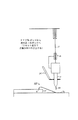
[002]ボールボンディングは、半導体ダイ上のボンドパッドを、ダイが取り付けられるリードフレームまたはその他の基板上の接点と相互接続するための一般的な技術である。ダイが樹脂封止された後に、ダイ上の回路をパッケージから延びるリードフレームのピンに電気的に接続するために、典型的には、電気的な配線ワイヤが、ダイの上面のボンドパッドから、リードフレーム上のリードフィンガーまで延びる。ダイのボンドパッドとリードフィンガーとの間のワイヤボンドは、一般的には、ボールボンディングマシンを用いて形成される。図1A〜図1Iは、従来技術によるボールボンディングにおけるステップを示す。従来のルーピング技術(本明細書では、順方向ルーピングと呼ばれる)は、金ワイヤの一端をダイ上のボンドパッドにボールボンディングし、ワイヤの他端をリードフレームにステッチボンディングすることを含む。より詳細には、ボールボンディングマシンを用いて、ワイヤ17は、一組のクランプ18に挿入され、そして、キャピラリー11の中心内腔に挿入される。プロセスの開始時点において、ワイヤ「テイル」23は、図1Aに示すように、キャピラリー11の先端から突き出ている。ワイヤ17の端部におけるテイル23は、電気的フレームオフ(EFO)と呼ばれるEFOワンド24からの電気スパーク16によって加熱される。スパークは、ワイヤの端部を溶かし、そして、その端部は、図1Bに示すように、それが溶けると、ボール19となる。クランプ18は、電流がクランプを介して戻るための経路を提供するために、EFO中には閉じられ、そして、ボール自身がキャピラリーの先端に着座するのを可能にするために開かれる。そして、キャピラリー11は、図1Cに示すように、ダイ15のボンドパッド13の上方における位置まで動かされる。
[002] Ball bonding is a common technique for interconnecting bond pads on a semiconductor die with contacts on a lead frame or other substrate to which the die is attached. After the die is resin sealed, electrical wiring wires are typically routed from the bond pads on the top surface of the die to electrically connect the circuitry on the die to the leadframe pins extending from the package. Extends to the lead fingers on the lead frame. The wire bond between the die bond pad and the lead finger is typically formed using a ball bonding machine. 1A-1I show steps in ball bonding according to the prior art. Conventional looping techniques (referred to herein as forward looping) include ball bonding one end of a gold wire to a bond pad on a die and stitch bonding the other end of the wire to a lead frame. More specifically, using a ball bonding machine, the
[003]そして、キャピラリー11は、キャピラリーの初期加速中に、クランプ18が開いたままの状態で下方へ動かされ、そして、キャピラリーの減速中に、クランプ18が閉じられ、そのために、キャピラリーの下方への運動中には、ボールは着座したままである。そして、クランプは、ボールがボンドパッド13に接触する直前に開く。ボール19は、図1Dに示すように、クランプ18が開いたままの状態で、ダイ15上のボンドパッド13に接触した状態となる。熱および/または超音波エネルギーが、ダイに加えられ、ボールを、ボンドパッド13にボンディングされた状態にする。このボンディングは、典型的には、ボールボンドまたは第1のボンドと呼ばれる。そして、クランプ18が開いた状態で、キャピラリー11は、図1Eに示すように、引き上げられ、ボールボンドの上面に取り付けられたままのワイヤが、わずかな長さだけ繰り出される。次に、クランプ18が開いた状態で、キャピラリー11は、予め定められたルーピング運動によって動かされ、ワイヤ(これは、ボールボンドに接続されたままである)は、キャピラリー11から一般的にはリードフィンガー21の近傍かつ上方における位置まで引きずられる。キャピラリー11が、リードフィンガー21の上方に配置されると、図1Fに示すように、クランプ18は閉じられる。そして、図1Gに示すように、キャピラリー11が引き下げられ、ワイヤをキャピラリーとリードフィンガー21の表面との間に挟む。この場合にも、ワイヤの挟まれた部分をリードフィンガー21にボンディングするために、熱および/または超音波エネルギーが加えられてもよい。このボンディングは、ステッチボンドまたは第2のボンドと呼ばれる。ここで、図1Hに示すように、クランプ18が、再び、開かれ、そして、キャピラリー11が、ワイヤがステッチボンドに取り付けられたままの状態で引き上げられ、それによって、余分のワイヤ「テイル」23が、キャピラリーから繰り出される。そして、クランプ18が、閉じられ、ステッチボンドロケーションに存在する最も弱い点においてワイヤテイル23を切断するために、キャピラリー11がさらに引き上げられる。完成した接続22は、ワイヤループと呼ばれ、図1Iに示される。
[003] The
[004]この時点において、キャピラリーは、ダイ上の次のボンドパッドのためのワイヤルーピングプロセスを開始するために、ダイ15の次のボンドパッドの近傍に動かされる。先行するワイヤループの形成を終了した後にキャピラリーの先端から突き出たままのワイヤテイル23は、上述したように、EFOによって溶かされ、次のボールボンディング処理を開始するために、次のボールを形成する。上述した従来の順方向ボールボンディング技術は、迅速で、信頼性が高く、かつ、安価である。しかしながら、それは、制限を有する。とりわけ、最小ループ高さは、通常、150ミクロンよりも高い。ループ高さは、ボンディング表面、例えば、ボンドパッドの上面の上方におけるワイヤの最大の高さとして定義される。より低いループ高さを実現することを試みることは、ワイヤループにネックダメージを発生させることがある。ネックは、ボールボンドに直接に隣接するワイヤループの部分である。ループ高さを150ミクロン以下に減少させることは、ネックの強度を減少させあるいはネックを切断する恐れがある。
[004] At this point, the capillary is moved in proximity to the next bond pad of die 15 to initiate the wire looping process for the next bond pad on the die. As described above, the
[005]より小さい集積回路パッケージングが、益々、要求されている。集積チップパッケージングの寸法を減少させることの意義のある特徴の1つは、それの厚さまたは高さを減少させることである。より薄いパッケージは、一般的に、当分野では、低プロフィールパッケージと呼ばれる。パッケージの高さを減少させるという要求は、ワイヤループの最も高い点の高さを減少させるという要求に対応し、それは、多くの場合、集積回路パッケージの高さに関する制約要因である。 [005] Smaller integrated circuit packaging is increasingly required. One significant feature of reducing the size of an integrated chip packaging is to reduce its thickness or height. Thinner packages are commonly referred to in the art as low profile packages. The requirement to reduce the height of the package corresponds to the requirement to reduce the height of the highest point of the wire loop, which is often a limiting factor regarding the height of the integrated circuit package.
[006]集積回路パッケージングおよびその他の目的に使用されるループの高さを減少させるために、逆方向ルーピングとして既知であるワイヤルーピング技術が開発された。逆方向ルーピングの背後にある前提は、ワイヤループの最も高い点はボールボンドに隣接するので、ルーピングプロセスを逆方向にすることは望ましいことであり、そのために、リードフレームの表面はダイの表面よりも低いので、リードフレーム(または、その他の基板)上に第1のボールボンドを形成し、そして、ダイのボンドパッド上に第2のステッチボンドを形成するということである。したがって、ワイヤループの最も高い点は、より低いボンディング表面の近くに存在し、それによって、全体の高さを減少させる。 [006] To reduce the height of loops used for integrated circuit packaging and other purposes, a wire looping technique known as reverse looping has been developed. The premise behind reverse looping is that it is desirable to reverse the looping process because the highest point of the wire loop is adjacent to the ball bond, so that the surface of the leadframe is better than the surface of the die The first ball bond is formed on the lead frame (or other substrate) and the second stitch bond is formed on the bond pad of the die. Thus, the highest point of the wire loop is near the lower bonding surface, thereby reducing the overall height.
[007]しかしながら、ルーピングプロセスの方向をただ単に逆にすることは、ステッチボンドはキャピラリーがボンディング表面に接触した状態になることを必要とするので、不可能である。ダイ上のボンドパッドは、通常、極めて小さく、そのために、キャピラリーを接触させずに、したがって、ダイ上の周囲の回路を損傷させずに、ダイのボンドパッド上にステッチボンドを形成することは困難である。さらに、ワイヤループは、ステッチボンドに近いそれらの最も低い点へたるむ傾向がある。したがって、ステッチボンドサイトが、ボールボンドサイトよりも高ければ、ワイヤは、ダイのエッジまたは上面に接触する可能性がある。これは、電気的な短絡またはワイヤの切断をもたらすことがある。 [007] However, simply reversing the direction of the looping process is not possible because stitchbonding requires the capillary to be in contact with the bonding surface. Bond pads on the die are usually very small, so it is difficult to form stitch bonds on the die bond pads without contacting the capillaries and thus without damaging the surrounding circuitry on the die It is. Furthermore, the wire loops tend to sag to their lowest point close to the stitch bond. Thus, if the stitch bond site is higher than the ball bond site, the wire may contact the edge or top surface of the die. This can lead to electrical shorts or wire cuts.
[008]そのために、図2A〜図2Cに示されるような逆方向ルーピング技術が開発され、この技術においては、第1のステップは、ボールボンドを形成するための本質的に標準的な技術に基づいてボールボンド25をダイ29上のボンドパッド27の上面に形成することである。しかしながら、従来の順方向ルーピング技術によってボールボンドを形成した後の場合と同じようにワイヤ17を繰り出す代わりに、キャピラリー11は引き上げられ、クランプ18は閉じられ、そして、キャピラリーは、さらに引き上げられ、ワイヤをボールボンドから切り離し、図2Aに示すように、ボンドパッド27上にボールボンド(バンプ)25だけを残す。そして、全部のワイヤルーピングプロセスが、逆方向に、すなわち、基板からボンドパッドまで実行される。すなわち、その後に、第2のボールボンド37が、リードフレーム39上に形成され、そして、キャピラリー11が、一連の運動によって動かされ、第1のボールボンド25の上方に配置され、図2Bに示すように、所望のワイヤループ形状を生成する。そして、ステッチボンド43が、第1のボールボンド(または、バンプ)25の上面に形成される。完成したワイヤループが、図2Cに示される。
[008] To that end, a reverse looping technique such as that shown in FIGS. 2A-2C has been developed, in which the first step is essentially a standard technique for forming ball bonds. Based on this, the
[009]この逆方向ルーピングプロセスは、低プロフィールパッケージングのための低いループ高さを提供することができる。しかしながら、それは、順方向ルーピングよりも極めて時間のかかるプロセスである。なぜなら、それは、1つのループごとに2つのボールボンドを形成しなければならないからである。さらに、ダイは、より大きな衝撃を受けなければならない。なぜなら、キャピラリーは、1つのワイヤループごとに2回、ダイ上にボンドを形成しなければならないからである(すなわち、1回目は、第1のボールボンドを生成するために、そして、2回目は、ボールボンドの上面にステッチボンドを生成するために)。逆方向ルーピングのもう1つの制約は、それが、しばしば、ダイ上のボンドパッドのピッチがどれほど微細であるかということに関する制約要因であることである。より詳細には、ダイボンドパッドの上面のバンプ25は、ステッチボンドを支持できるほど十分に大きいものでなければならない。さらに、ステッチボンドが、それの上面に形成されるとき、バンプの直径は、横方向に増加する。
[009] This reverse looping process can provide a low loop height for low profile packaging. However, it is a much more time consuming process than forward looping. This is because two ball bonds must be formed for each loop. In addition, the die must be subjected to greater impact. This is because the capillary must form a bond on the die twice for each wire loop (ie, the first time to generate the first ball bond and the second time To produce a stitch bond on the top surface of the ball bond). Another limitation of reverse looping is that it is often a constraint on how fine the bond pad pitch on the die is. More specifically, the
[010]したがって、本発明の目的は、改善されたワイヤループ形成方法およびその装置を提供することである。 [010] Accordingly, it is an object of the present invention to provide an improved wire loop forming method and apparatus.
[011]本発明の別の目的は、極めて低いループ高さを備えるワイヤループ配線を提供することである。 [011] Another object of the present invention is to provide wire loop wiring with extremely low loop height.
[012]本発明によれば、ボールボンドをダイボンドパッド上に形成することによって、バンプがそのボンドパッド上に形成される。そして、ワイヤを切断せずに、かつ、クランプを開いた状態で、キャピラリーが、調整された一連のxyz運動をなし、ボールボンドの上面においてワイヤを折り曲げる。そして、ワイヤは、テイルを切断することなく、バンプの上面にステッチボンディングされる。調整されたさらなる一連のxyz運動がこれに続き、キャピラリーを第2のボンドサイト(例えば、リードフレームまたはその他の基板)へ動かし、基板上において第2のステッチボンドを実行し、そして、テイルを切断し、プロセスを完了する。 [012] According to the present invention, a bump is formed on a bond pad by forming a ball bond on the die bond pad. And without cutting the wire and with the clamp open, the capillary performs a series of coordinated xyz motions to fold the wire at the top surface of the ball bond. The wire is then stitch bonded to the upper surface of the bump without cutting the tail. This is followed by a further series of coordinated xyz movements that move the capillary to a second bond site (eg, a lead frame or other substrate), perform a second stitch bond on the substrate, and cut the tail And complete the process.
[013]上述したワイヤ折り曲げ部を形成するための本発明の特定の一実施形態によれば、ボールボンドが形成され、そして、キャピラリーが、指定された高さ(本明細書では、分離高さと呼ばれる)だけz方向に引き上げられる。そして、キャピラリーは、一般的には第2のボンドロケーションから遠ざかるような方向に指定された距離(本明細書では、折り曲げオフセット距離と呼ばれる)だけ水平方向に(xy平面において)動かされる。キャピラリーは、再度、さらに別の距離(本明細書では、折り曲げ係数と呼ばれる)だけz方向に引き上げられてもよく、あるいは、引き上げられなくてもよい。上述したステッチボンドをバンプの上面に形成するために、xy平面における別の運動がこれに続き、一般的には、キャピラリーをバンプの上面に逆戻りさせる。そして、調整された別のxyz運動がこれに続き、キャピラリーを第2のボンドサイトの(例えば、リードフレーム上の)ロケーションへ動かし、そこで、第2のステッチボンドが形成される。 [013] According to one particular embodiment of the present invention for forming the wire fold described above, a ball bond is formed and the capillary has a specified height (herein a separation height and Is called) in the z direction. The capillary is then moved horizontally (in the xy plane) by a specified distance (referred to herein as the fold offset distance) in a direction generally away from the second bond location. The capillary may or may not be raised again in the z-direction by yet another distance (referred to herein as the folding factor). In order to form the above-described stitch bond on the top surface of the bump, another movement in the xy plane follows, typically reversing the capillary back to the top surface of the bump. This is followed by another coordinated xyz motion that moves the capillary to a location (eg, on the lead frame) at the second bond site where a second stitch bond is formed.
[022]図3は、本発明に基づいて形成された折り曲げられた順方向ワイヤループ45の側面絵画図である。図3は、それの上面にボンドパッド53を含む集積回路ダイ51、およびボンドパッド53とリードフレーム55との間のワイヤループ配線を備えるリードフレーム基板55を示す。ワイヤループ45は、本発明の技術に基づいて形成され、5つの基本的な構成要素を備えると考えることができる。図3を参照すると、それらは、(1)バンプ56、(2)バンプの上面に存在するワイヤ折り曲げ部57、(3)バンプの上面に存在するステッチボンド58、(4)第1のボンドサイトと第2のボンドサイトとを相互接続するワイヤループ59、および(5)第2のステッチボンド60である。
[022] FIG. 3 is a side pictorial view of a folded forward wire loop 45 formed in accordance with the present invention. FIG. 3 shows an integrated circuit die 51 including a bond pad 53 on its upper surface, and a lead frame substrate 55 comprising wire loop wiring between the bond pad 53 and the lead frame 55. The wire loop 45 is formed based on the technique of the present invention and can be considered to comprise five basic components. Referring to FIG. 3, they are (1)
[023]上述した5つの基本的な構成要素は、ボールボンディングマシンを用いて形成されてもよい。 [023] The five basic components described above may be formed using a ball bonding machine.
[024]図5A〜図5Oは、本発明の特定の一実施形態に基づいて折り曲げられた順方向ワイヤループを形成するための例示的なプロセスの様々なステージにおけるボールボンディングマシンのキャピラリーの位置およびワイヤの状態を示す。本明細書において使用される用語において、垂直方向はz方向と呼ばれ、水平方向はxy方向と呼ばれる。本出願における図面は、当然ながら、2次元であり、そのために、すべてのxy運動は、紙面の平面内に存在するように示され、したがって、単純に、1次元の運動として、すなわち、xy運動ではなく、x運動またはy運動であると考えてもよい。しかしながら、現実の世界において、与えられたダイ上のワイヤループは、すべてがお互いに平行であるとは限らないので、ボールボンディングマシンのキャピラリーの運動を制御する機械コードにおいては、すべての横方向の運動は、xy運動として定義されなければならない。したがって、本明細書においては、同じ用語が、使用される。さらに、垂直という用語および水平という用語は、ダイの上面が水平に配置されるという仮定に基づいた単なる例示的なものであり、その仮定は、典型的なものではあるが、常に当然な仮定であるとは限らない。 [024] FIGS. 5A-5O illustrate the position of the capillary of the ball bonding machine at various stages of an exemplary process for forming a folded forward wire loop in accordance with one particular embodiment of the invention and Shows the state of the wire. In terms used herein, the vertical direction is called the z direction and the horizontal direction is called the xy direction. The drawings in this application are, of course, two-dimensional, so that all xy motions are shown to be in the plane of the page, and therefore simply as one-dimensional motions, ie xy motions. Instead, it may be considered an x motion or a y motion. However, in the real world, the wire loops on a given die are not all parallel to each other, so in the machine code that controls the movement of the capillary of a ball bonding machine, all lateral directions Motion must be defined as xy motion. Accordingly, the same terms are used herein. In addition, the terms vertical and horizontal are merely exemplary based on the assumption that the top surface of the die is positioned horizontally, and that assumption is typical but always a natural assumption. Not always.
[025]図5Aに示すように、折り曲げられた順方向ループを形成するプロセスは、先行するルーピングプロセスの終了時点におけるキャピラリー11から開始し、ワイヤテイル23が、キャピラリーから延び、かつ、クランプ18は閉じられている。キャピラリーは、ダイ63のボンドパッド61および関連するリードフィンガー65の近傍に配置され、それらのボンドパッド61とリードフィンガー65との間に、次のワイヤループ配線が、形成されることになる。
[025] As shown in FIG. 5A, the process of forming the folded forward loop begins with the capillary 11 at the end of the preceding looping process, the
[026]ワイヤは、電気的フレームオフ67によって溶かされ、ワイヤの端部が溶かされる。溶けるとき、それは、その性質上、図5Bに示すように、ボール72を形成する。図5Cに示すように、キャピラリーが引き下げられ、ボンドパッド61に向かって動かされる。そして、キャピラリーは引き下げられ、ボール72をボンドパッド61に接触させる。熱および/または超音波エネルギーが加えられ、ボールをボンドパッドにボンディングする。図5Dは、この時点におけるプロセスを示し、これは、本質的には、折り曲げられた順方向のワイヤループの第1の部分、すなわち、バンプ56を形成することの終了時点である。
[026] The wire is melted by an electrical frame-off 67 and the ends of the wire are melted. When melted, it forms a
[027]次に、バンプ56の上面から延びるワイヤを所定の長さだけ繰り出すために、キャピラリー11が、クランプ18が開いた状態で上昇する。この上昇の距離は、本明細書では、分離高さと呼ばれ、図4において、符号75で示される。図5Eは、このステップの後のキャピラリーの位置を示す。そして、キャピラリー11は、xy平面において、第2のボンドサイト65への方向とは一般的に反対の第1の方向に移動する(図5A〜図5Cにおいて、左へ)。好ましくは、折り曲げオフセットの方向は、第2のボンドサイト65へのxy方向とは正反対である。このxy運動の距離は、本明細書では、折り曲げオフセットと呼ばれ、図4において、符号76で示される。折り曲げオフセット運動の後のキャピラリーの位置が、図5Fに示される。
[027] Next, in order to feed out the wire extending from the upper surface of the
[028]本発明の実施形態の中には、折り曲げオフセット運動の終了時点において、キャピラリー11が、再度、わずかな距離(本明細書では、折り曲げ係数と呼ばれる)だけ引き上げられ(正のz方向へ)、ワイヤをさらに繰り出すものもある。折り曲げ係数は、図4において、符号77で示される。しかしながら、本発明の用途によっては、ゼロの折り曲げ係数が、適切であるものもある。図5Gは、プロセスのこの時点におけるキャピラリーおよびワイヤの位置を示す。折り曲げオフセットおよび折り曲げ係数は、ワイヤ折り曲げ部におけるワイヤの量を制御する。
[028] In some embodiments of the present invention, at the end of the fold offset motion, the capillary 11 is again lifted (in the positive z direction) by a small distance (referred to herein as the fold factor). ), And there are some that let out the wire further. The bending coefficient is indicated by
[029]そして、キャピラリー11は、バンプ56に向かって逆方向に動かされ、バンプ56自身の上面にワイヤを折り返し、バンプの上面にワイヤ折り曲げ部を形成することを開始する。図5Hは、キャピラリーが折り曲げ部を形成するために移動しているときのキャピラリー11の位置およびワイヤの状態を示す。この最後に述べた運動は、図4において符号78で示されるように、本明細書では、折り曲げ戻し運動と呼ばれる。好ましくは、折り曲げ戻し運動は、折り曲げオフセット運動のxy方向とは正反対のxy方向である。折り曲げ係数77がゼロである実施形態においては、折り曲げ戻し運動は、好ましくは、完全に水平な運動(すなわち、xy運動)である。折り曲げ係数77が、ゼロでなければ、折り曲げ戻し運動78は、ボールボンディング中にキャピラリーが存在していたときと同じ高さにまでキャピラリーを戻すために、負のz成分を含んでもよい。いずれの場合にも、折り曲げ戻し運動の終了時点において、キャピラリーを分離高さにまで戻す。しかしながら、これは、必要条件ではない。実際には、本発明の少なくともいくつかの好ましい実施形態においては、以下でさらに説明するように、キャピラリーは、分離高さよりも低い高さに戻る。実際には、折り曲げ戻し運動78は、折り曲げ係数77がたとえゼロであっても、正の(上方への)または負の(下方への)z成分を含んでもよい。重要な特徴は、ワイヤ折り曲げ部が、バンプ56の上面に形成され、好ましくは、第2のボンドサイト65から遠ざかる方向へまっすぐに延びることである。分離高さと折り曲げ戻し運動78の終了時点におけるキャピラリーの位置との差は、本明細書では、バンプ高さと呼ばれる。それは、正の値であってもよく、あるいは、負の値であってもよい。しかしながら、上述したように、本発明の実施形態によっては、分離高さに到達することとワイヤ折り曲げ部の完成および/または折り曲げ係数との間にキャピラリーのz運動が存在しないものもあり、折り曲げ戻し運動のz成分は、正確に等しくかつ反対方向であり、そのために、バンプ高さは、ゼロとなる。
[029] Then, the capillary 11 is moved in the opposite direction toward the
[030]さらに、折り曲げ戻し運動78の水平成分は、折り曲げオフセット運動と同じ距離でなくてもよい。特定の用途によっては、折り曲げオフセット運動の前のキャピラリーの元々のxy座標よりも短い位置(図4において経路78aによって示されるように)、その元々のxy座標と正確に同じの位置(図4において経路78bによって示されるように)、あるいは、その元々のxy座標よりも長い位置(図4において経路78cによって示されるように)においてステッチボンドを実行するために、ある特定の位置に戻ることが望ましい。
[030] Further, the horizontal component of the folding back
[031]バンプが形成されたときのキャピラリーのxy位置とこの時点におけるキャピラリーのxy座標との水平方向における差は、折り曲げ戻しオフセットと呼ばれる。換言すれば、折り曲げ戻しオフセットは、折り曲げオフセット運動と折り曲げ戻し運動の水平方向成分とのxy次元における差である。折り曲げ戻し運動78のxy成分が、折り曲げオフセット運動76よりも小さければ、折り曲げ戻しオフセットは、正の値として表現される。折り曲げ戻し運動78の水平方向成分が、折り曲げオフセット運動76よりも長ければ、折り曲げ戻しオフセットは、負の値として表現される。折り曲げオフセット運動76と折り曲げ戻し運動78とが、同じxy(すなわち、水平方向)の量を有するならば、折り曲げ戻しオフセットはゼロである。
[031] The difference in the horizontal direction between the xy position of the capillary when the bump is formed and the xy coordinate of the capillary at this time point is called the folding back offset. In other words, the folding back offset is the difference in the xy dimension between the folding offset motion and the horizontal component of the folding back motion. If the xy component of the folding back
[032]折り曲げ戻し運動の終了時点において、キャピラリーは、図5Iに示すように、バンプ56の上面に接触しており、かつ、キャピラリー11の先端とバンプとの間にワイヤを挟んでいる。この時点において、ワイヤは、挟まれてはいるが、切断されてはいない。また、この時点において、折り曲げられた順方向ワイヤループ全体の上述した5つの部分の中の2番目(すなわち、折り曲げ部57)が完成する。プロセスの開始時点から、ワイヤは、切断されておらず、したがって、折り曲げ部57は、バンプ56と接続している。
[032] At the end of the folding back movement, as shown in FIG. 5I, the capillary is in contact with the upper surface of the
[033]そして、ワイヤは、バンプ56の上面にステッチボンディングされる。ワイヤの押しつけられた部分をバンプ56の上面にボンディングするのを助けるために、熱および/または超音波エネルギーが加えられてもよい。この時点において、ループ全体の上述した5つの部分の中の3番目(すなわち、第1のステッチボンド58)が、完成する。図5Jは、この時点におけるプロセスを示し、これは、本質的には、図5Iに示される位置と同じである。なぜなら、キャピラリーは、典型的には、ステッチボンディング中に移動しないからである。
[033] The wire is then stitch bonded to the upper surface of the
[034]ここで、キャピラリーは、所望のワイヤループ形状(ループ全体の第4の部分)を形成しかつキャピラリーを第2のボンドサイト65の上方に配置するために、一連の調整されたxyz運動によって、第2のボンドサイトに近づくように動かされる。図5Kおよび図5Lは、第2のボンドサイト65までの例示的な軌跡に沿った2つの点におけるキャピラリー11の位置を示す。
[034] Here, the capillary forms a desired wire loop shape (the fourth part of the entire loop) and a series of coordinated xyz motions to position the capillary above the
[035]調整されたxyz運動は、第2のボンドサイトに近づくような直線のxy運動からなる比較的に単純なものであってもよい。しかしながら、典型的には、最も好ましい形状になるようにワイヤループを形成するのを助けるz方向への運動が存在する。プロセスの開始時点から、ワイヤは、まだ、切断されていないので、ワイヤループ59は、第1のボンドサイトにおいて、バンプ56、折り曲げ部57、およびステッチボンド58と接続している。
[035] The coordinated xyz motion may be relatively simple, consisting of a linear xy motion that approaches the second bond site. However, there is typically a movement in the z direction that helps form the wire loop to the most preferred shape. Since the wire has not yet been cut from the start of the process, the
[036]次に、キャピラリーが引き下げられ、第2のボンド表面65とキャピラリー11の先端との間にワイヤを挟み、そして、ワイヤが、第2のボンドサイトにステッチボンディングされる。ボンディングを助けるために、熱および/または超音波エネルギーが、加えられてもよい。この時点において、ワイヤは、図5Mに示すように、挟まれてはいるが、完全には切断されていない。そして、キャピラリー11が、クランプ18が依然として開いた状態で、かつ、ワイヤが依然として第2のステッチボンド60に取り付けられた状態で引き上げられ、それによって、ワイヤテイル69が、キャピラリー11から繰り出される。図5Nは、プロセスのこの時点におけるキャピラリーの位置を示す。そして、図5Oに示すように、第2のステッチボンド60においてワイヤを切断するために、クランプ18が閉じられ、キャピラリー11がさらに引き上げられる。ここで、折り曲げられた順方向ワイヤループ全体の中の第5の部分、すなわち、第2のステッチボンド60が完成し、折り曲げ順方向ルーピングプロセス全体が完了する。
[036] Next, the capillary is pulled down, a wire is sandwiched between the
[037]バンプ56の主たる目的は、キャピラリーがボンドパッドに直接に接触するのを防止することであり、かつ、ワイヤが第1のボンドサイトから引き出される高さ(z方向)を高くすることである。より詳細には、ワイヤは、バンプの上面からワイヤループが開始することによって提供されるダイ表面の上方の余分な高さがもしなければ、ワイヤループ59が第1のボンドサイトと第2のボンドサイトとの中間に存在するダイ表面にあるいは接触する可能性のある低い位置において第1のボンドサイトから引き出される。
[037] The main purpose of the
[038]折り曲げ部57をバンプの上面に形成することの主たる目的は、ワイヤが、第1のボンドサイトから一般的には水平方向に引き出され、第2のボンドサイトに向けて延ばされ、それによって、低いループ高さをもたらすことである。折り曲げ部は、一般的には、形状が楕円形であり、その楕円形の長軸は、xy平面に存在し、ワイヤは、折り曲げ部の端部を水平方向に引き出され、そして、一般的には、第2のボンドサイトに向けて直接に延ばされる。このような方向を有する配置は、従来の順方向ワイヤループにおいてワイヤが第1のボンドサイトから引き出されるときに一般的にはまっすぐに上方向へ配置されるワイヤと対照されるべきである。このように、本発明のルーピング技術は、極めて低いループ高さを提供する。なぜなら、ワイヤは、ボールボンドサイトから引き出され、垂直に上方向にではなく水平方向に延ばされるからである。 [038] The main purpose of forming the bend 57 on the upper surface of the bump is to pull the wire from the first bond site in a generally horizontal direction and to the second bond site, Thereby providing a low loop height. The bend is typically elliptical in shape, its long axis is in the xy plane, the wire is drawn horizontally at the end of the bend, and generally Is extended directly towards the second bond site. An arrangement having such a direction should be contrasted with a wire that is typically placed straight up when the wire is pulled from the first bond site in a conventional forward wire loop. Thus, the looping technique of the present invention provides a very low loop height. This is because the wire is drawn from the ball bond site and extends vertically rather than vertically upward.
[039]さらに、ダイに与える衝撃は、従来の逆方向ボールボンディングと比較すれば減少する。なぜなら、それは、逆方向ルーピングの場合のように、通常の第2のボンドをバンプの上面において実行しないからである。逆方向ボンディングの場合における図7Bに類似する通常のステッチボンドと比較すれば、図7Aに示すように、ワイヤは、ほんのわずかに押しつけられ、ループおよびボールの上面のステッチボンドを形成する。 [039] Furthermore, the impact on the die is reduced compared to conventional reverse ball bonding. This is because the normal second bond is not performed on the top surface of the bump as in the case of reverse looping. Compared to a normal stitch bond similar to FIG. 7B in the case of reverse bonding, as shown in FIG. 7A, the wire is only slightly pressed to form a stitch bond on the top surface of the loop and ball.
[040]さらに、本発明によれば、逆方向ボールボンディングと比較して、より微細なピッチを実現することができる。なぜなら、バンプは、逆方向ワイヤルーピング技術の場合と同じほどには、押しつけられず、そして、横方向に押しつぶされないからである。 [040] Furthermore, according to the present invention, a finer pitch can be realized as compared to reverse ball bonding. This is because the bumps are not squeezed and crushed laterally as in the reverse wire looping technique.
[041]ワイヤボンディングマシンは、本明細書で説明されたプロセスをマシンに実行させることのできる制御回路を備える運動制御システムによって制御される。一般的には、回路は、プログラムされた汎用コンピュータのようなディジタル処理装置、ディジタル信号プロセッサー、ステートマシン、組み合わせ論理回路、マイクロプロセッサー、特定用途向け集積回路、または、その他の何らかの既知であるディジタル処理手段を備える。回路が、コンピュータを備える場合、本発明は、限定はされないが、その大部分が、本明細書で説明されたプロセスを実行するようにワイヤボンディングマシンを制御するためにコンピュータをプログラムするソフトウェア内に存在してもよい。 [041] The wire bonding machine is controlled by a motion control system that includes control circuitry that can cause the machine to perform the processes described herein. Generally, the circuit is a digital processing device such as a programmed general purpose computer, a digital signal processor, a state machine, a combinatorial logic circuit, a microprocessor, an application specific integrated circuit, or some other known digital processing. Means. If the circuit comprises a computer, the present invention is, but not limited to, mostly in software that programs the computer to control the wire bonding machine to perform the processes described herein. May be present.
[042]図4を参照して説明された様々な運動成分を最適化することによって、低いループ高さを備えかつネックダメージのない所望の形状を達成することができる。一例として、図6は、図7に示される折り曲げ部を形成しその後に図8Aおよび図8Bに示されるループプロフィールを形成するのに使用された例示的なパラメータを示す。最初の3つの運動(分離高さ75、折り曲げオフセット76、および折り曲げ係数77)は、折り曲げ部におけるワイヤの量および折り曲げ部の形状を集合的に決定する。これらの運動が、大きすぎる場合、所望の折り曲げ部よりも大きな折り曲げ部が形成される可能性がある。これらの運動が、小さすぎる場合、折り曲げ部は、まったく形成されない可能性があり、ワイヤのネック領域が損傷を受ける可能性がある。
[042] By optimizing the various motion components described with reference to FIG. 4, a desired shape with low loop height and no neck damage can be achieved. As an example, FIG. 6 shows exemplary parameters used to form the bend shown in FIG. 7 and subsequently form the loop profile shown in FIGS. 8A and 8B. The first three movements (
[043]本発明者らは、実験によって、ワイヤ直径よりもわずかに大きい分離高さおよび折り曲げオフセット(例えば、ワイヤ直径の約1.01倍〜約1.55倍)は優れた結果を達成できることを見出している。さらに、折り曲げ係数は、正の値であるべきである。図7の例においては、1ミルのワイヤ直径の場合、分離高さ75は、1.5ミルであり、折り曲げオフセット76は、1.3ミルであり、そして、折り曲げ係数77は1ミルである。これらの設定値は、適切な量のワイヤを繰り出し、折り曲げ戻し運動78が開始する前に、垂直線から約30°だけワイヤを曲げる。
[043] We have experimentally shown that separation heights and bending offsets slightly larger than the wire diameter (eg, about 1.01 to about 1.55 times the wire diameter) can achieve excellent results. Is heading. Furthermore, the folding factor should be a positive value. In the example of FIG. 7, for a 1 mil wire diameter, the
[044]折り曲げ戻し運動78は、バンプの最終的な形状を決定する。本発明者らが使用した特定のマシンにおいては、折り曲げ戻し運動78は、2つのパラメータが指定された。より詳細には、(1)上述した折り曲げ戻しオフセットパラメータ(これは、折り曲げオフセットとともに、折り曲げ戻し運動の水平方向成分を決定する)、および(2)バンプ高さ(これは、折り曲げ係数とともに、戻し運動の垂直方向成分を決定する)である。
[044] The fold back
[045]バンプを過度に平坦化することなく、折り曲げ部を支持するための十分な変形を備える良好な折り曲げ部を形成するために、バンプは、通常、負の値であるべきである(バンプ高さは、分離高さからの垂直方向距離である)。この例においては、バンプ高さは、−1.25ミルであり、分離高さは、1.5ミルである。したがって、キャピラリーの最終的な位置は、約0.25ミルだけバンプ56の上方にある。これは、過不足のないワイヤの平坦化を提供し、バンプを大きく平坦化することなく、折り曲げ部を形成する。この例における折り曲げ戻しオフセットは、0.5ミルであり、これは、折り曲げ戻し運動78の後のキャピラリーの最終的な位置がバンプの中心から0.5ミルだけ水平方向に(第2のボンド60から遠ざかるように)ずらされることを意味する。これらの設定値は、ステッチボンド58のサイトがバンプ56の上面の中心に配置されることを保証する。
[045] In order to form a good fold with sufficient deformation to support the fold without over-planarizing the bump, the bump should usually have a negative value (bump Height is the vertical distance from the separation height). In this example, the bump height is -1.25 mil and the separation height is 1.5 mil. Thus, the final location of the capillary is approximately 0.25 mil above the
[046]これらのパラメータを用いたボンディングから得られたワイヤループが、図8に示される。複数の実験サンプルのすべてにおいて、これらのパラメータを用いた平均ループ高さは、2.3ミルであった。最大ループ高さは、2.5ミルであった。 [046] A wire loop obtained from bonding using these parameters is shown in FIG. In all of the experimental samples, the average loop height using these parameters was 2.3 mils. The maximum loop height was 2.5 mil.
[047]本発明のいくつかの特定の実施形態を説明したが、当業者は、様々な変形、変更、および改良を容易に考え出すことができる。本明細書から明らかなそのような変形、変更、および改良は、ここには明示的に述べられてはいないが、本明細書の一部と解釈されるべきであり、本発明の精神および範囲に含められる。したがって、これまでの説明は、ただ単に例にすぎず、また、本発明を限定するものではない。本発明は、特許請求の範囲に定義されるものによってのみ、かつ、それらに同等なものによってのみ、限定される。 [047] Although several specific embodiments of the invention have been described, those skilled in the art can readily devise various variations, modifications, and improvements. Such variations, modifications, and improvements apparent from the specification are not expressly stated herein but are to be construed as part of the specification, and are within the spirit and scope of the invention. Included in Accordingly, the foregoing description is by way of example only and is not intended to limit the invention. The invention is limited only as defined in the following claims and the equivalents thereto.
11…キャピラリー、13…ボンドパッド、15…ダイ、17…ワイヤ、18…クランプ、21…リードフィンガー、23…テイル。
DESCRIPTION OF
Claims (37)
ワイヤを前記第1のボンドロケーションにボールボンディングし、前記第1のボンドロケーション上にバンプを形成するステップ(1)と、
ワイヤの折り曲げ部を前記ボールボンドの上面に形成するステップ(2)であって、前記ワイヤの折り曲げ部が、前記ボールボンドに接続されている、形成するステップ(2)と、
前記ワイヤの折り曲げ部を前記ボールボンドの上面にステッチボンディングするステップ(3)と、
前記ワイヤ折り曲げ部と前記第2のボンドサイトとの間にワイヤループを連続的に形成するステップ(4)と、
前記第2のボンドサイトにおいて、前記ワイヤをステッチボンディングし、前記ワイヤループを終端するステップ(5)と、
を備える方法。 A method of forming a wire loop interconnect between a first bond site and a second bond site, comprising:
Ball bonding a wire to the first bond location and forming a bump on the first bond location;
Forming a bent portion of the wire on the upper surface of the ball bond (2), wherein the bent portion of the wire is connected to the ball bond; and
(3) stitch bonding the bent portion of the wire to the upper surface of the ball bond;
Forming a wire loop continuously between the wire bend and the second bond site (4);
Stitching the wire at the second bond site and terminating the wire loop (5);
A method comprising:
ステップ(2)が、
キャピラリーをボールボンドの上方へ垂直方向に引き上げるステップ(2.1)と、
キャピラリーを前記第2のボンドサイトから遠ざかるように水平方向に動かすステップ(2.2)と、
キャピラリーを前記第2のボンドサイトに向かって戻るような方向へ水平方向に動かすステップ(2.3)と、
を備える、請求項1に記載の方法。 The wire loop is formed by a ball bonding machine comprising at least a capillary;
Step (2)
Pulling the capillary vertically above the ball bond (2.1);
Moving the capillary horizontally away from the second bond site (2.2);
Moving the capillary horizontally in a direction to return toward the second bond site (2.3);
The method of claim 1, comprising:
ステップ(2.2)とステップ(2.3)との間において、キャピラリーを引き上げるステップ(2.4)、
をさらに備える、請求項5に記載の方法。 Step (2)
Between step (2.2) and step (2.3), pulling up the capillary (2.4),
The method of claim 5, further comprising:
(1)前記第1のボンドロケーションにおけるボールボンドと、
(2)前記ボールボンドに接続するワイヤを備える前記ボールボンドの上面に存在するワイヤの折り曲げ部であって、前記ワイヤの折り曲げ部が、前記ボールボンドの上面にステッチボンディングされた、ワイヤ折り曲げ部と、
(3)前記ワイヤ折り曲げ部と前記第2のボンドサイトとの間に存在するワイヤループであって、前記ワイヤループが、前記ワイヤ折り曲げ部に接続するワイヤを備える、ワイヤループと、
(4)前記ワイヤループを終端する前記第2のボンドサイトにおけるステッチボンドと、
を備えるワイヤループ相互コネクタ。 A wire loop interconnect between a first bond site and a second bond site, comprising:
(1) a ball bond at the first bond location;
(2) A wire bent portion existing on an upper surface of the ball bond including a wire connected to the ball bond, wherein the wire bent portion is stitch-bonded to the upper surface of the ball bond; ,
(3) A wire loop that exists between the wire bending portion and the second bond site, the wire loop including a wire connected to the wire bending portion;
(4) a stitch bond at the second bond site that terminates the wire loop;
Wire loop interconnection connector comprising.
ワイヤとともにキャピラリーを有するワイヤボンディングマシンを用いて、ボールボンドを第1のボンドロケーションに形成するステップ(1)と、
前記キャピラリーを第1の高さまで引き上げ、それによって、前記ボールボンドに取り付けられたワイヤが、前記キャピラリーから繰り出されるステップ(2)と、
前記キャピラリーを第1の距離だけ第1の方向に水平方向に動かすステップ(3)と、
前記キャピラリーを前記第1の水平方向とは実質的に反対の第2の水平方向に動かすステップ(4)と、
第1のステッチボンドを前記ボールボンドの上面に形成するステップ(5)と、
前記第1のボンドサイトから所定の距離だけ離れた第2のボンドサイトまで前記キャピラリーを動かすステップ(6)と、
第2のステッチボンドを前記第2のボンドサイトに形成するステップ(7)と、
前記第2のボンドサイトに隣接する前記ワイヤを切断するステップ(8)と、
を備える方法。 A method of forming a wire loop for electrically interconnecting semiconductors, comprising:
Forming a ball bond at a first bond location using a wire bonding machine having a capillary with the wire (1);
Raising the capillary to a first height, whereby the wire attached to the ball bond is unwound from the capillary (2);
Moving the capillary horizontally in a first direction by a first distance; (3);
Moving the capillary in a second horizontal direction substantially opposite the first horizontal direction (4);
Forming a first stitch bond on the top surface of the ball bond (5);
Moving the capillary to a second bond site that is a predetermined distance away from the first bond site;
Forming a second stitch bond at the second bond site (7);
Cutting the wire adjacent to the second bond site (8);
A method comprising:
キャピラリーと、
前記キャピラリーの内腔を介してワイヤを供給するためのワイヤ送り出しシステムと、
前記キャピラリーの運動を制御するための運動制御システムと
を備え、
前記運動制御システムが、
(1)ボールボンドを第1のボンドロケーションに形成し、
(2)前記ボールボンドに接続するワイヤの折り曲げ部を前記ボールボンドの上面に形成し、
(3)前記ワイヤの折り曲げ部を前記ボールボンドの上面にステッチボンディングし、
(4)前記ワイヤ折り曲げ部と第2のボンドサイトとの間にワイヤループを連続的に形成し、
(5)ステッチボンドを前記第2のボンドサイトに形成して前記ワイヤループを終端するための、
回路を含む、ワイヤボンディングマシン。 A wire bonding machine,
Capillary,
A wire delivery system for supplying a wire through the lumen of the capillary;
A motion control system for controlling the motion of the capillary,
The motion control system comprises:
(1) forming a ball bond at a first bond location;
(2) forming a bent portion of a wire connected to the ball bond on the upper surface of the ball bond;
(3) stitch bonding the bent portion of the wire to the upper surface of the ball bond;
(4) A wire loop is continuously formed between the wire bent portion and the second bond site,
(5) forming a stitch bond at the second bond site to terminate the wire loop;
Wire bonding machine including circuit.
(2.1)キャピラリーをボールボンドの上方に垂直方向に引き上げ、
(2.2)キャピラリーを前記第2のボンドサイトから遠ざかるように水平方向に動かし、
(2.3)前記第1のボンドサイトに向かって戻るような方向へ水平方向にキャピラリーを動かすための、
回路を備える、請求項27に記載のワイヤボンディングマシン。 The circuit for performing task (2) comprises:
(2.1) Pull up the capillary vertically above the ball bond,
(2.2) Move the capillary horizontally away from the second bond site;
(2.3) For moving the capillary in the horizontal direction in such a direction as to return toward the first bond site,
28. The wire bonding machine of claim 27, comprising a circuit.
前記コンピュータ可読プロダクトが、
(1)ボールボンドを前記第1のボンドロケーションに形成し、
(2)前記ボールボンドに接続するワイヤの折り曲げ部を前記ボールボンドの上面に形成し、
(3)前記ワイヤの折り曲げ部を前記ボールボンドの上面にステッチボンディングおよびテイルボンディングし、
(4)前記ワイヤ折り曲げ部と前記第2のボンドサイトとの間にワイヤループを連続的に形成し、
(5)ステッチボンドを前記第2のボンドサイトに形成して前記ワイヤループを終端するための、
コンピュータ実行可能命令を備える、コンピュータ可読プロダクト。 A computer readable product for controlling a wire bonding machine comprising a capillary,
The computer readable product is
(1) forming a ball bond at the first bond location;
(2) forming a bent portion of a wire connected to the ball bond on the upper surface of the ball bond;
(3) Stitch bonding and tail bonding of the bent portion of the wire to the upper surface of the ball bond;
(4) A wire loop is continuously formed between the wire bent portion and the second bond site,
(5) forming a stitch bond at the second bond site to terminate the wire loop;
A computer readable product comprising computer executable instructions.
(2.1)キャピラリーをボールボンドの上方に垂直方向に引き上げ、
(2.2)キャピラリーを前記第2のボンドサイトから遠ざかるように水平方向に動かし、
(2.3)前記第1のボンドサイトに向かって戻るような方向へ水平方向にキャピラリーを動かすための、
コンピュータ実行可能命令を備える、請求項36に記載のコンピュータ可読プロダクト。
The computer executable instructions for forming the wire bend are
(2.1) Pull up the capillary vertically above the ball bond,
(2.2) Move the capillary horizontally away from the second bond site;
(2.3) For moving the capillary in the horizontal direction in such a direction as to return toward the first bond site,
40. The computer readable product of claim 36, comprising computer executable instructions.
Applications Claiming Priority (3)
| Application Number | Priority Date | Filing Date | Title |
|---|---|---|---|
| US52530503P | 2003-11-26 | 2003-11-26 | |
| US10/988,053 US7347352B2 (en) | 2003-11-26 | 2004-11-12 | Low loop height ball bonding method and apparatus |
| PCT/US2004/039676 WO2005055282A2 (en) | 2003-11-26 | 2004-11-24 | Low loop height ball bonding method and apparatus |
Publications (2)
| Publication Number | Publication Date |
|---|---|
| JP2007512714A true JP2007512714A (en) | 2007-05-17 |
| JP2007512714A5 JP2007512714A5 (en) | 2008-01-24 |
Family
ID=34595261
Family Applications (1)
| Application Number | Title | Priority Date | Filing Date |
|---|---|---|---|
| JP2006541443A Pending JP2007512714A (en) | 2003-11-26 | 2004-11-24 | Low loop height ball bonding method and apparatus |
Country Status (5)
| Country | Link |
|---|---|
| US (2) | US7347352B2 (en) |
| JP (1) | JP2007512714A (en) |
| SG (1) | SG123792A1 (en) |
| TW (1) | TWI367533B (en) |
| WO (1) | WO2005055282A2 (en) |
Cited By (1)
| Publication number | Priority date | Publication date | Assignee | Title |
|---|---|---|---|---|
| US10221396B2 (en) | 2009-06-05 | 2019-03-05 | FUJIFILM Cellular Dynamics, Inc. | Reprogramming T cells and hematopoietic cells |
Families Citing this family (25)
| Publication number | Priority date | Publication date | Assignee | Title |
|---|---|---|---|---|
| US7229906B2 (en) | 2002-09-19 | 2007-06-12 | Kulicke And Soffa Industries, Inc. | Method and apparatus for forming bumps for semiconductor interconnections using a wire bonding machine |
| US7464854B2 (en) * | 2005-01-25 | 2008-12-16 | Kulicke And Soffa Industries, Inc. | Method and apparatus for forming a low profile wire loop |
| DE102006011352A1 (en) * | 2005-03-23 | 2006-10-05 | Unaxis International Trading Ltd. | Method for producing a wire connection |
| US8016182B2 (en) * | 2005-05-10 | 2011-09-13 | Kaijo Corporation | Wire loop, semiconductor device having same and wire bonding method |
| JP2009503822A (en) * | 2005-07-26 | 2009-01-29 | マイクロボンズ・インコーポレイテッド | System and method for assembling packaged integrated circuits using insulated wire bonds |
| JP4530984B2 (en) * | 2005-12-28 | 2010-08-25 | 株式会社新川 | Wire bonding apparatus, bonding control program, and bonding method |
| US20080286959A1 (en) * | 2007-05-14 | 2008-11-20 | Texas Instruments Incorporated | Downhill Wire Bonding for QFN L - Lead |
| WO2007134317A1 (en) * | 2006-05-15 | 2007-11-22 | Texas Instruments Incorporated | Downhill wire bonding for semiconductor device |
| CN101505905A (en) * | 2006-10-18 | 2009-08-12 | 库利克和索夫工业公司 | Improved conductive bumps, wire loops including the improved conductive bumps, and methods of forming the same |
| JP5481769B2 (en) * | 2006-11-22 | 2014-04-23 | 日亜化学工業株式会社 | Semiconductor device and manufacturing method thereof |
| US8637394B2 (en) * | 2007-07-05 | 2014-01-28 | Stats Chippac Ltd. | Integrated circuit package system with flex bump |
| CN101971313B (en) * | 2008-01-30 | 2013-07-24 | 库力索法工业公司 | Wire loop and method of forming the wire loop |
| JP4625858B2 (en) * | 2008-09-10 | 2011-02-02 | 株式会社カイジョー | Wire bonding method, wire bonding apparatus, and wire bonding control program |
| JP4344002B1 (en) | 2008-10-27 | 2009-10-14 | 株式会社新川 | Wire bonding method |
| JP5062283B2 (en) | 2009-04-30 | 2012-10-31 | 日亜化学工業株式会社 | Semiconductor device and manufacturing method thereof |
| DE102009029040A1 (en) * | 2009-08-31 | 2011-03-03 | Robert Bosch Gmbh | Apparatus and method for manufacturing a device |
| JP2012004464A (en) * | 2010-06-18 | 2012-01-05 | Toshiba Corp | Semiconductor device, method of manufacturing the semiconductor device, and apparatus for manufacturing the semiconductor device |
| US7918378B1 (en) | 2010-08-06 | 2011-04-05 | National Semiconductor Corporation | Wire bonding deflector for a wire bonder |
| US20120032354A1 (en) * | 2010-08-06 | 2012-02-09 | National Semiconductor Corporation | Wirebonding method and device enabling high-speed reverse wedge bonding of wire bonds |
| CN102412167B (en) | 2010-09-25 | 2016-02-03 | 飞思卡尔半导体公司 | What engage for line fixes |
| CN102487025B (en) | 2010-12-08 | 2016-07-06 | 飞思卡尔半导体公司 | For the long supporter in conjunction with wire |
| US8609525B2 (en) * | 2011-03-21 | 2013-12-17 | Stats Chippac Ltd. | Integrated circuit packaging system with interconnects and method of manufacture thereof |
| MY181180A (en) * | 2011-09-09 | 2020-12-21 | Carsem M Sdn Bhd | Low loop wire bonding |
| TWI543284B (en) * | 2014-02-10 | 2016-07-21 | 新川股份有限公司 | Method for producing semiconductor apparatus and wire bonding apparatus |
| GB2615441A (en) * | 2020-12-23 | 2023-08-09 | Skyworks Solutions Inc | Apparatus and methods for tool mark free stitch bonding |
Citations (4)
| Publication number | Priority date | Publication date | Assignee | Title |
|---|---|---|---|---|
| JPH0951011A (en) * | 1995-08-10 | 1997-02-18 | Tanaka Denshi Kogyo Kk | Wire bonding method of semiconductor chip |
| JP2004172477A (en) * | 2002-11-21 | 2004-06-17 | Kaijo Corp | Wire loop form, semiconductor device having the same, wire bonding method, and semiconductor manufacturing apparatus |
| JP2004289153A (en) * | 2003-03-24 | 2004-10-14 | Texas Instr Inc <Ti> | Wire-bonding for semiconductor package |
| JP2005019778A (en) * | 2003-06-27 | 2005-01-20 | Shinkawa Ltd | Wire bonding method |
Family Cites Families (24)
| Publication number | Priority date | Publication date | Assignee | Title |
|---|---|---|---|---|
| US4437604A (en) | 1982-03-15 | 1984-03-20 | Kulicke & Soffa Industries, Inc. | Method of making fine wire interconnections |
| US4824005A (en) | 1986-08-13 | 1989-04-25 | Orthodyne Electronics Corporation | Dual mode ultrasonic generator in a wire bonding apparatus |
| JPH04273135A (en) | 1991-02-27 | 1992-09-29 | Shinkawa Ltd | Wire bonding method |
| US5111989A (en) * | 1991-09-26 | 1992-05-12 | Kulicke And Soffa Investments, Inc. | Method of making low profile fine wire interconnections |
| JP3152764B2 (en) | 1992-10-21 | 2001-04-03 | 株式会社東芝 | Wire bonder |
| US5421503A (en) * | 1994-08-24 | 1995-06-06 | Kulicke And Soffa Investments, Inc. | Fine pitch capillary bonding tool |
| US5842628A (en) * | 1995-04-10 | 1998-12-01 | Fujitsu Limited | Wire bonding method, semiconductor device, capillary for wire bonding and ball bump forming method |
| JP3370539B2 (en) * | 1997-01-13 | 2003-01-27 | 株式会社新川 | Wire bonding method |
| JP3413340B2 (en) | 1997-03-17 | 2003-06-03 | 株式会社新川 | Wire bonding method |
| JP3455092B2 (en) * | 1997-10-27 | 2003-10-06 | 株式会社新川 | Semiconductor device and wire bonding method |
| JP2000082717A (en) * | 1998-09-07 | 2000-03-21 | Shinkawa Ltd | Wire bonding method |
| JP3522123B2 (en) * | 1998-09-30 | 2004-04-26 | 株式会社新川 | Wire bonding method |
| JP2000114304A (en) * | 1998-10-08 | 2000-04-21 | Shinkawa Ltd | Wire bonding method |
| JP2000174054A (en) | 1998-12-04 | 2000-06-23 | Kaijo Corp | Apparatus for forming ball for wire bonder |
| JP3457196B2 (en) | 1998-12-22 | 2003-10-14 | 株式会社カイジョー | Ball bonding method |
| JP3932235B2 (en) | 1999-02-25 | 2007-06-20 | 株式会社カイジョー | Ball forming apparatus and method for wire bonder |
| JP3913134B2 (en) | 2002-08-08 | 2007-05-09 | 株式会社カイジョー | Bump forming method and bump |
| JP2003100793A (en) | 2001-09-25 | 2003-04-04 | Kaijo Corp | Method of wire bonding |
| JP3765778B2 (en) | 2002-08-29 | 2006-04-12 | ローム株式会社 | Capillary for wire bonding and wire bonding method using the same |
| US7229906B2 (en) | 2002-09-19 | 2007-06-12 | Kulicke And Soffa Industries, Inc. | Method and apparatus for forming bumps for semiconductor interconnections using a wire bonding machine |
| US7494042B2 (en) * | 2003-10-02 | 2009-02-24 | Asm Technology Singapore Pte. Ltd. | Method of forming low wire loops and wire loops formed using the method |
| US20060011710A1 (en) * | 2004-07-13 | 2006-01-19 | Asm Technology Singapore Pte Ltd | Formation of a wire bond with enhanced pull |
| US7188759B2 (en) * | 2004-09-08 | 2007-03-13 | Kulicke And Soffa Industries, Inc. | Methods for forming conductive bumps and wire loops |
| JP4298665B2 (en) * | 2005-02-08 | 2009-07-22 | 株式会社新川 | Wire bonding method |
-
2004
- 2004-11-12 US US10/988,053 patent/US7347352B2/en active Active
- 2004-11-24 WO PCT/US2004/039676 patent/WO2005055282A2/en active Application Filing
- 2004-11-24 SG SG200604112A patent/SG123792A1/en unknown
- 2004-11-24 JP JP2006541443A patent/JP2007512714A/en active Pending
- 2004-11-26 TW TW093136568A patent/TWI367533B/en active
-
2007
- 2007-11-20 US US11/942,997 patent/US7584881B2/en active Active
Patent Citations (4)
| Publication number | Priority date | Publication date | Assignee | Title |
|---|---|---|---|---|
| JPH0951011A (en) * | 1995-08-10 | 1997-02-18 | Tanaka Denshi Kogyo Kk | Wire bonding method of semiconductor chip |
| JP2004172477A (en) * | 2002-11-21 | 2004-06-17 | Kaijo Corp | Wire loop form, semiconductor device having the same, wire bonding method, and semiconductor manufacturing apparatus |
| JP2004289153A (en) * | 2003-03-24 | 2004-10-14 | Texas Instr Inc <Ti> | Wire-bonding for semiconductor package |
| JP2005019778A (en) * | 2003-06-27 | 2005-01-20 | Shinkawa Ltd | Wire bonding method |
Cited By (1)
| Publication number | Priority date | Publication date | Assignee | Title |
|---|---|---|---|---|
| US10221396B2 (en) | 2009-06-05 | 2019-03-05 | FUJIFILM Cellular Dynamics, Inc. | Reprogramming T cells and hematopoietic cells |
Also Published As
| Publication number | Publication date |
|---|---|
| US20050109819A1 (en) | 2005-05-26 |
| TW200524068A (en) | 2005-07-16 |
| TWI367533B (en) | 2012-07-01 |
| US7347352B2 (en) | 2008-03-25 |
| WO2005055282A2 (en) | 2005-06-16 |
| US7584881B2 (en) | 2009-09-08 |
| WO2005055282A3 (en) | 2006-02-09 |
| US20080111252A1 (en) | 2008-05-15 |
| SG123792A1 (en) | 2006-07-26 |
Similar Documents
| Publication | Publication Date | Title |
|---|---|---|
| JP2007512714A (en) | Low loop height ball bonding method and apparatus | |
| TWI306278B (en) | Method and apparatus for forming bumps for semiconductor interconnections using a wire bonding machine | |
| US8048720B2 (en) | Wire loop and method of forming the wire loop | |
| EP1422014B1 (en) | Semiconductor device having a wire loop with a crushed part on a ball, loop wire bonding method and loop wire bonding apparatus for carrying out such method | |
| CN104813455B (en) | The manufacture method of lead wire connecting apparatus and semiconductor device | |
| US8152046B2 (en) | Conductive bumps, wire loops, and methods of forming the same | |
| US4068371A (en) | Method for completing wire bonds | |
| TWI248186B (en) | Method for producing a wedge-wedge wire connection | |
| KR102443487B1 (en) | Advancedly strengthened electrical interconnections for semiconductor devices and methods for forming the same | |
| US7214606B2 (en) | Method of fabricating a wire bond with multiple stitch bonds | |
| US6933223B1 (en) | Ultra-low loop wire bonding | |
| US6270000B1 (en) | Wire bonding method | |
| TWI739379B (en) | Semiconductor device, semiconductor device manufacturing method, and wire bonding device | |
| US20240128228A1 (en) | Security wire over stitch bond | |
| KR100660821B1 (en) | Wire bonding method | |
| TWI816255B (en) | Wire bonding structure, bonding structure forming method, and electronic device | |
| WO2022259328A1 (en) | Wire bonding device and wire bonding method | |
| JP7386526B2 (en) | Wire bonding equipment and wire bonding method | |
| JP5048990B2 (en) | Semiconductor device and manufacturing method thereof | |
| JP2004319921A (en) | Wire bonding method | |
| CN116250067A (en) | Wire bonding method and method for manufacturing semiconductor device | |
| JPH0590320A (en) | Ball type wire bonding method | |
| TW202038351A (en) | Wire-bonding device, fabrication method of semiconductor device, and semiconductor device which can further reduce the arc height | |
| JPH08316260A (en) | Wire bonding method and semiconductor manufacturing apparatus | |
| CN1886226A (en) | Low loop height ball bonding method and apparatus |
Legal Events
| Date | Code | Title | Description |
|---|---|---|---|
| A521 | Request for written amendment filed |
Free format text: JAPANESE INTERMEDIATE CODE: A523 Effective date: 20071126 |
|
| A621 | Written request for application examination |
Free format text: JAPANESE INTERMEDIATE CODE: A621 Effective date: 20071126 |
|
| A977 | Report on retrieval |
Free format text: JAPANESE INTERMEDIATE CODE: A971007 Effective date: 20100907 |
|
| A131 | Notification of reasons for refusal |
Free format text: JAPANESE INTERMEDIATE CODE: A131 Effective date: 20100914 |
|
| A02 | Decision of refusal |
Free format text: JAPANESE INTERMEDIATE CODE: A02 Effective date: 20110222 |