JP2007282195A - Camera lens module and manufacturing method therefor - Google Patents
Camera lens module and manufacturing method therefor Download PDFInfo
- Publication number
- JP2007282195A JP2007282195A JP2007042616A JP2007042616A JP2007282195A JP 2007282195 A JP2007282195 A JP 2007282195A JP 2007042616 A JP2007042616 A JP 2007042616A JP 2007042616 A JP2007042616 A JP 2007042616A JP 2007282195 A JP2007282195 A JP 2007282195A
- Authority
- JP
- Japan
- Prior art keywords
- substrate
- camera lens
- lens module
- image sensor
- sensor chip
- Prior art date
- Legal status (The legal status is an assumption and is not a legal conclusion. Google has not performed a legal analysis and makes no representation as to the accuracy of the status listed.)
- Pending
Links
- 238000004519 manufacturing process Methods 0.000 title claims abstract description 24
- 239000000758 substrate Substances 0.000 claims abstract description 99
- 239000011521 glass Substances 0.000 claims description 29
- 230000002093 peripheral effect Effects 0.000 claims description 15
- 239000002390 adhesive tape Substances 0.000 claims description 12
- 230000003287 optical effect Effects 0.000 abstract description 2
- 238000000034 method Methods 0.000 description 13
- 238000010438 heat treatment Methods 0.000 description 11
- 239000000853 adhesive Substances 0.000 description 8
- 230000001070 adhesive effect Effects 0.000 description 8
- 239000000428 dust Substances 0.000 description 7
- 239000012535 impurity Substances 0.000 description 6
- 230000006866 deterioration Effects 0.000 description 2
- 230000017525 heat dissipation Effects 0.000 description 2
- 238000004806 packaging method and process Methods 0.000 description 2
- 238000007789 sealing Methods 0.000 description 2
- 230000000694 effects Effects 0.000 description 1
- 238000005516 engineering process Methods 0.000 description 1
- 230000014509 gene expression Effects 0.000 description 1
- 238000003384 imaging method Methods 0.000 description 1
- 238000012986 modification Methods 0.000 description 1
- 230000004048 modification Effects 0.000 description 1
- 239000002245 particle Substances 0.000 description 1
- 238000003825 pressing Methods 0.000 description 1
- 230000005855 radiation Effects 0.000 description 1
- 229910000679 solder Inorganic materials 0.000 description 1
- 239000000126 substance Substances 0.000 description 1
Images


Classifications
-
- H—ELECTRICITY
- H01—ELECTRIC ELEMENTS
- H01L—SEMICONDUCTOR DEVICES NOT COVERED BY CLASS H10
- H01L27/00—Devices consisting of a plurality of semiconductor or other solid-state components formed in or on a common substrate
- H01L27/14—Devices consisting of a plurality of semiconductor or other solid-state components formed in or on a common substrate including semiconductor components sensitive to infrared radiation, light, electromagnetic radiation of shorter wavelength or corpuscular radiation and specially adapted either for the conversion of the energy of such radiation into electrical energy or for the control of electrical energy by such radiation
- H01L27/144—Devices controlled by radiation
- H01L27/146—Imager structures
- H01L27/14601—Structural or functional details thereof
- H01L27/14625—Optical elements or arrangements associated with the device
-
- H—ELECTRICITY
- H01—ELECTRIC ELEMENTS
- H01L—SEMICONDUCTOR DEVICES NOT COVERED BY CLASS H10
- H01L27/00—Devices consisting of a plurality of semiconductor or other solid-state components formed in or on a common substrate
- H01L27/14—Devices consisting of a plurality of semiconductor or other solid-state components formed in or on a common substrate including semiconductor components sensitive to infrared radiation, light, electromagnetic radiation of shorter wavelength or corpuscular radiation and specially adapted either for the conversion of the energy of such radiation into electrical energy or for the control of electrical energy by such radiation
- H01L27/144—Devices controlled by radiation
- H01L27/146—Imager structures
- H01L27/14683—Processes or apparatus peculiar to the manufacture or treatment of these devices or parts thereof
-
- H—ELECTRICITY
- H05—ELECTRIC TECHNIQUES NOT OTHERWISE PROVIDED FOR
- H05K—PRINTED CIRCUITS; CASINGS OR CONSTRUCTIONAL DETAILS OF ELECTRIC APPARATUS; MANUFACTURE OF ASSEMBLAGES OF ELECTRICAL COMPONENTS
- H05K13/00—Apparatus or processes specially adapted for manufacturing or adjusting assemblages of electric components
-
- H—ELECTRICITY
- H05—ELECTRIC TECHNIQUES NOT OTHERWISE PROVIDED FOR
- H05K—PRINTED CIRCUITS; CASINGS OR CONSTRUCTIONAL DETAILS OF ELECTRIC APPARATUS; MANUFACTURE OF ASSEMBLAGES OF ELECTRICAL COMPONENTS
- H05K3/00—Apparatus or processes for manufacturing printed circuits
- H05K3/30—Assembling printed circuits with electric components, e.g. with resistor
- H05K3/303—Surface mounted components, e.g. affixing before soldering, aligning means, spacing means
- H05K3/305—Affixing by adhesive
-
- H—ELECTRICITY
- H05—ELECTRIC TECHNIQUES NOT OTHERWISE PROVIDED FOR
- H05K—PRINTED CIRCUITS; CASINGS OR CONSTRUCTIONAL DETAILS OF ELECTRIC APPARATUS; MANUFACTURE OF ASSEMBLAGES OF ELECTRICAL COMPONENTS
- H05K2201/00—Indexing scheme relating to printed circuits covered by H05K1/00
- H05K2201/10—Details of components or other objects attached to or integrated in a printed circuit board
- H05K2201/10613—Details of electrical connections of non-printed components, e.g. special leads
- H05K2201/10621—Components characterised by their electrical contacts
- H05K2201/10674—Flip chip
-
- H—ELECTRICITY
- H05—ELECTRIC TECHNIQUES NOT OTHERWISE PROVIDED FOR
- H05K—PRINTED CIRCUITS; CASINGS OR CONSTRUCTIONAL DETAILS OF ELECTRIC APPARATUS; MANUFACTURE OF ASSEMBLAGES OF ELECTRICAL COMPONENTS
- H05K2203/00—Indexing scheme relating to apparatus or processes for manufacturing printed circuits covered by H05K3/00
- H05K2203/04—Soldering or other types of metallurgic bonding
- H05K2203/049—Wire bonding
Abstract
Description
本発明はカメラレンズモジュールおよびその製造方法に関し、特にフリップチップ構造を有する低背構造のカメラレンズモジュールおよびその製造方法に関する。 The present invention relates to a camera lens module and a manufacturing method thereof, and more particularly to a low-profile camera lens module having a flip chip structure and a manufacturing method thereof.
チップオンボード(COB)パッケージ法は、集積回路(IC)パッケージ技法の一種であり、裸のICチップを回路基板又はサブストレート上に直接マウントする。これは、(1)チップマウンティング、(2)ワイヤ接続および(3)シール(封止)の3つの基本技術を組み合わせ、回路基板組立工程のIC製造のパッケージおよびテスト工程へ送る。このCOBパッケージ法は、コンピュータ、携帯電話、時計、電子玩具やカルキュレータ等の最近の各種電子デバイスに応用されている。 Chip-on-board (COB) packaging is a type of integrated circuit (IC) packaging technique in which a bare IC chip is mounted directly on a circuit board or substrate. This combines three basic technologies: (1) chip mounting, (2) wire connection, and (3) sealing (sealing), and sends it to the IC manufacturing package and test process in the circuit board assembly process. This COB package method is applied to various electronic devices such as computers, mobile phones, watches, electronic toys and calculators.
図5を参照して従来技術について説明する。図5は、従来のカメラレンズモジュールの断面図を示す。図示する従来のカメラレンズモジュール5は、COBパケージ法を採用し、ホルダ51、ガラス板(プレート)55、イメージセンサチップ58およびサブストレート56を含んでいる。
The prior art will be described with reference to FIG. FIG. 5 shows a cross-sectional view of a conventional camera lens module. The illustrated conventional camera lens module 5 employs the COB package method, and includes a
ここで、ホルダ51は、チャンバ(部屋)52およびレンズグループ用の内ねじ54が形成された内周壁を有する。ガラス板55は、ホルダ51の内ねじ54の下方に配置され且つホルダ51に接合されている。イメージセンサチップ58は、ホルダ51のチャンバ52の下方にガラス板55とコリメート(位置合わせ)されて配置されている。サブストレート56は、ホルダ51の底面511に配置されている。イメージセンサチップ58は、導電性又は非導電性接着剤によりサブストレート56に接続され、その後ベーキング(加熱)して固着されている。導電性ワイヤ57を採用して、イメージセンサチップ58とサブストレート56を接続し、その後接着剤を使用してサブストレート56をホルダ51の底面511に固着する。その後、サブストレート56は熱工程により固定される。更に、フレキシブルサブストレート61およびサブストレート56を半田59により相互に固着される。
Here, the
上述の如き従来のカメラレンズモジュール5は、比較的大きい高さを有するので、斯かるカメラレンズモジュール5は小型又は超小型の電子装置には使用不可能である。更に、イメージセンサチップ58は放熱特性が制限され且つ埃や不純物等の粒子状の異物がガラス板55の表面551に沈着すると、清掃不能であるので撮影特性を低化させることになる。従って、従来のカメラレンズモジュールは、上述の如き点において改善改良の余地がある。
Since the conventional camera lens module 5 as described above has a relatively large height, the camera lens module 5 cannot be used for a small or ultra-small electronic device. Further, the heat radiation characteristics of the
本発明によるカメラレンズモジュールおよびその製造方法は、上述した課題に鑑みなされたものであり、上述の如き課題を解消又は低減する新たなカメラレンズモジュールおよびその製造方法を提供することを目的とする。 The camera lens module and the manufacturing method thereof according to the present invention have been made in view of the above-described problems, and an object thereof is to provide a new camera lens module and a manufacturing method thereof that eliminate or reduce the above-described problems.
即ち、本発明の1つの目的は、サブストレートをイメージセンサチップ上に配置することにより高さを効果的に抑えると共に(組立製造時又はその後の使用時に)埃やその他の粒子状異物が侵入することによる上述した課題を軽減し且つサブストレートに開口を設けて放熱特性を改善するカメラレンズモジュールを提供することである。また、本発明の他の目的は、斯かるカメラレンズモジュールの製造方法を提供することである。 That is, one object of the present invention is to effectively suppress the height by arranging the substrate on the image sensor chip (at the time of assembly manufacture or subsequent use), and dust and other particulate foreign substances enter. It is an object of the present invention to provide a camera lens module that reduces the above-described problems and improves the heat dissipation characteristics by providing an opening in the substrate. Another object of the present invention is to provide a method for manufacturing such a camera lens module.
本発明によるカメラレンズモジュールおよびその製造方法は、次の如き特徴的な構成を採用している。 The camera lens module and the manufacturing method thereof according to the present invention employ the following characteristic configuration.
(1)レンズを収容するチャンバを有するホルダ、前記レンズから入射するイメージを検出するイメージセンサチップおよび該イメージセンサチップに電気的に接続されるサブストレートを含むカメラレンズモジュールにおいて、
前記サブストレートは開口を有し、前記ホルダは前記開口と位置合わせして前記サブストレートの一面に配置され、前記イメージセンサチップは前記開口と位置合わせして前記サブストレートの前記ホルダと反対面に配置されるカメラレンズモジュール。
(2)前記サブストレートの前記ホルダが配置された面側にガラス板を配置して前記ホルダの前記開口を覆う上記(1)のカメラレンズモジュール。
(3)前記イメージセンサチップは前記サブストレートに異方導電性フィルムを介して加熱および加圧して接続される上記(1)又は(2)のカメラレンズモジュール。
(4)前記サブストレートには受動部品が配置される上記(1)、(2)又は(3)のカメラレンズモジュール。
(5)前記イメージセンサチップを覆うように前記サブストレートの前記反対面に固定され、開口を有するカバーを更に備える上記(1)、(2)、(3)又は(4)のカメラレンズモジュール。
(6)前記ホルダの内周壁の前記サブストレート側近傍には両面接着テープが設けられる上記(1)乃至(5)の何れかのカメラレンズモジュール。
(7)前記サブストレートはフレキシブルサブストレートである上記(1)乃至(6)の何れかのカメラレンズモジュール。
(8)前記ホルダおよび前記イメージセンサチップを収容するスロット手段を更に備える上記(1)乃至(4)の何れかのカメラレンズモジュール。
(9)前記スロット手段および前記サブストレートを接続する導電性部材を更に備える上記(8)のカメラレンズモジュール。
(10)前記ホルダの内周壁には内ねじが形成されている上記(1)乃至(9)の何れかのカメラレンズモジュール。
(11)サブストレートに開口を形成するステップと、
前記サブストレートの一面に前記開口に位置合わせしてレンズを収容するホルダを固定するステップと、
前記サブストレートの他面に前記開口に位置合わせしてイメージセンサチップを配置するステップと、
前記サブストレートおよび前記イメージセンサチップを異方導電性フィルムにより電気的接続するステップと、
を備えるカメラレンズモジュールの製造方法。
(12)前記サブストレートの前記一面に前記開口を覆うガラス板を配置するステップを更に備える上記(11)のカメラレンズモジュールの製造方法。
(13)前記サブストレートの前記他面にカバーを配置して前記イメージセンサチップを覆うステップを更に備える上記(11)又は(12)のカメラレンズモジュールの製造方法。
(14)スロット手段により前記ホルダおよび前記イメージセンサチップを収容するステップを更に備える上記(11)又は(12)のカメラレンズモジュールの製造方法。
(15)前記サブストレートの前記他面の前記イメージセンサチップの外周部に受動部品を配置するステップを更に備える上記(11)乃至(14)の何れかのカメラレンズモジュールの製造方法。
(1) In a camera lens module including a holder having a chamber for housing a lens, an image sensor chip for detecting an image incident from the lens, and a substrate electrically connected to the image sensor chip,
The substrate has an opening, the holder is disposed on one surface of the substrate in alignment with the opening, and the image sensor chip is aligned with the opening on the surface opposite to the holder of the substrate. Camera lens module to be placed.
(2) The camera lens module according to (1), wherein a glass plate is disposed on a surface side of the substrate on which the holder is disposed to cover the opening of the holder.
(3) The camera lens module according to (1) or (2), wherein the image sensor chip is connected to the substrate by heating and pressing through an anisotropic conductive film.
(4) The camera lens module according to (1), (2), or (3), wherein passive components are arranged on the substrate.
(5) The camera lens module according to (1), (2), (3), or (4), further including a cover fixed to the opposite surface of the substrate so as to cover the image sensor chip and having an opening.
(6) The camera lens module according to any one of (1) to (5), wherein a double-sided adhesive tape is provided in the vicinity of the substrate side of the inner peripheral wall of the holder.
(7) The camera lens module according to any one of (1) to (6), wherein the substrate is a flexible substrate.
(8) The camera lens module according to any one of (1) to (4), further including slot means for accommodating the holder and the image sensor chip.
(9) The camera lens module according to (8), further including a conductive member that connects the slot means and the substrate.
(10) The camera lens module according to any one of (1) to (9), wherein an inner screw is formed on an inner peripheral wall of the holder.
(11) forming an opening in the substrate;
Fixing a holder for accommodating a lens in alignment with the opening on one surface of the substrate;
Placing the image sensor chip in alignment with the opening on the other surface of the substrate;
Electrically connecting the substrate and the image sensor chip with an anisotropic conductive film;
A method for manufacturing a camera lens module.
(12) The method for manufacturing a camera lens module according to (11), further including a step of arranging a glass plate covering the opening on the one surface of the substrate.
(13) The method for manufacturing a camera lens module according to (11) or (12), further including a step of disposing a cover on the other surface of the substrate to cover the image sensor chip.
(14) The method for manufacturing a camera lens module according to (11) or (12), further including a step of accommodating the holder and the image sensor chip by a slot means.
(15) The method for manufacturing a camera lens module according to any one of (11) to (14), further including a step of disposing a passive component on an outer peripheral portion of the image sensor chip on the other surface of the substrate.
本発明のカメラレンズモジュールおよびその製造方法によると、次の如き実用上の特有の効果を奏する。即ち、全体の高さを抑えた低背構造のカメラレンズモジュールが得られる。その理由は、サブストレートの一面(上面)にホルダを配置し、他面(下面)にイメージセンサチップを配置し、サブストレートおよびイメージセンサチップ間を密着接続するからである。また、ガラス板とイメージセンサチップ間のサブストレートは、イメージセンサチップに対応位置に開口を有するので、イメージセンサチップの発熱を効果的に放熱可能である。更に、チャンバを形成する内周壁の下部に両面接着テープを使用して埃や不純物を付着させることにより、ガラス板の上面を清潔に維持し、撮像性能の低下(劣化)を防止可能である。従って、小型(又は薄型)デジタルカメラや撮影機能を有する携帯電話等の小型薄形化が要求されるカメラレンズモジュールに好適である。 According to the camera lens module and the manufacturing method thereof of the present invention, there are the following practical specific effects. That is, a low-profile camera lens module with a reduced overall height can be obtained. The reason is that the holder is disposed on one surface (upper surface) of the substrate, the image sensor chip is disposed on the other surface (lower surface), and the substrate and the image sensor chip are closely connected. Moreover, since the substrate between the glass plate and the image sensor chip has an opening at a position corresponding to the image sensor chip, the heat generated by the image sensor chip can be effectively radiated. Furthermore, by using a double-sided adhesive tape to attach dust and impurities to the lower part of the inner peripheral wall that forms the chamber, the upper surface of the glass plate can be kept clean, and deterioration (deterioration) in imaging performance can be prevented. Therefore, it is suitable for a camera lens module that is required to be small and thin, such as a small (or thin) digital camera or a mobile phone having a photographing function.
一方、本発明のカメラレンズモジュールの製造方法によると、複雑、時間を要し且つ高価な設備を必要とする加工や処理を不要として、簡単な加熱等の熱処理によりカメラレンズモジュールを安価に製造することが可能である。サブストレートとイメージセンサチップ間を例えば異方導電性フィルム等により相互接続することが可能である。 On the other hand, according to the method for manufacturing a camera lens module of the present invention, a camera lens module is manufactured at low cost by heat treatment such as simple heating without requiring processing or processing that requires complicated, time-consuming and expensive equipment. It is possible. The substrate and the image sensor chip can be interconnected by, for example, an anisotropic conductive film.
以下、本発明によるカメラレンズモジュールおよびその製造方法の好適実施の形態の構成および動作を、添付図面を参照して詳細に説明する。 Hereinafter, the configuration and operation of a preferred embodiment of a camera lens module and a manufacturing method thereof according to the present invention will be described in detail with reference to the accompanying drawings.
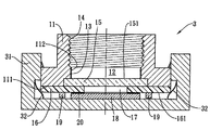
先ず、図1は、本発明によるカメラレンズモジュールの第1実施の形態の構成を示す断面図である。このカメラレンズモジュール1は、ホルダ11、ガラス板15、サブストレート(基板)16およびイメージセンサチップ(CCD等の撮像素子)18により構成されている。そして、ホルダ11はチャンバ12を有し、ホルダ11の内周壁112の下部には両面接着テープ13が設けられ、ホルダ11の内周壁112の上部にはレンズ群又は光学系(図示せず)用の内ねじ14が形成されている。ガラス板15は、ホルダ11のチャンバ12の下方に配置される。サブストレート16は、ホルダ11の下面111に配置され且つホルダ11のチャンバ12と位置合わせされた開口17を有し、サブストレート16の下面161には受動部品19が配置されている。イメージセンサチップ18は、サブストレート16の下面161に接続され且つサブストレート16の開口17と位置合わせされている。両面接着テープ13は、ガラス板15上の埃や不純物等を付着させて捕獲し、ガラス板15の上面151を清潔に維持する。
First, FIG. 1 is a sectional view showing a configuration of a first embodiment of a camera lens module according to the present invention. The camera lens module 1 includes a
尚、ここで上面および下面等の表現は、図面に関する位置関係を述べるに過ぎず、カメラレンズモジュールの使用状態により上下関係が反転することに留意されたい。これは、後述するカメラレンズモジュールの他の実施の形態についても同様である。 It should be noted that the expressions such as the upper surface and the lower surface here merely describe the positional relationship with respect to the drawing, and the vertical relationship is inverted depending on the use state of the camera lens module. The same applies to other embodiments of the camera lens module described later.
イメージセンサチップ18は、異方導電性フィルム20を加熱してサブストレート16の低面161に接続され、イメージセンサチップ18の入出力デバイス(又はパッド)およびサブストレート16の入出力デバイス間を相互接続する。次に、サブストレート16は接着剤によりホルダ11の低面111に接合され、加熱工程により固着される。
The
次に、図2の断面図を参照して本発明によるカメラレンズモジュールの第2実施の形態を説明する。図2に示す第2実施の形態のカメラレンズモジュール2において、上述した第1実施の形態のカメラレンズモジュール1と対応する構成要素には、説明の便宜上同様の参照符号を使用する(尚、後述する他の実施の形態についても同様である)。本発明によるカメラレンズモジュール2は、ホルダ11、ガラス板15、フレキシブル(可撓性)サブストレート21、イメージセンサチップ18およびカバー23により構成される。
Next, a second embodiment of the camera lens module according to the present invention will be described with reference to a sectional view of FIG. In the camera lens module 2 of the second embodiment shown in FIG. 2, the same reference numerals are used for the components corresponding to the camera lens module 1 of the first embodiment described above for convenience of explanation (note that it will be described later) The same applies to the other embodiments. The camera lens module 2 according to the present invention includes a
カメラレンズモジュール2において、ホルダ11はチャンバ12を有し、ホルダ11の内周壁112の下部には両面接着テープ13が設けられ、内周壁112の上部にはレンズ群(図示せず)用の内ねじ14が形成されている。ガラス板15は、ホルダ11のチャンバ12の下に配置されている。フレキシブルサブストレート21は、ホルダ11の底面111には位置され且つホルダ11のチャンバ12と位置合わせされた開口212を有し、フレキシブルサブストレート21の底面211には受動部品19が設けられている。イメージセンサチップ18は、フレキシブルサブストレート21の底面211に接続され且つフレキシブルサブストレート21の開口212と位置合わせされている。カバー23は、開口22を有し且つフレキシブルサブストレート21の底面211に固定されている。両面接着テープ13は、ガラス板15上の埃や不純物を付着させてガラス板15の上面151を清潔に維持する。
In the camera lens module 2, the
イメージセンサチップ18は、異方導電性フィルム20を加熱および加圧してフレキシブルサブストレート21の底面211に接続され、イメージセンサチップ18の入出力デバイスおよびフレキシブルサブストレートの入出力デバイス間を相互接続する。次に、フレキシブルサブストレート21は、接着剤によりホルダ11の底面111に接合され且つ加熱して固着される。カバー23は、接着剤によりフレキシブルサブストレート21の底面に固定され、カバー23の開口22はイメージセンサチップ18の下に位置し、外力が加えられることによりイメージセンサチップ18が破損するのを防止する。また、カバー23の開口22は、イメージセンサチップ18の放熱に有効である。
The
次に、図3の断面図を参照して、本発明による第3実施の形態のカメラレンズモジュール3について説明する。このカメラレンズモジュール3は、ホルダ11、ガラス板15、サブストレート16、イメージセンサチップ18およびスロット手段31により構成される。
Next, a camera lens module 3 according to a third embodiment of the present invention will be described with reference to the sectional view of FIG. The camera lens module 3 includes a
第3実施の形態のカメラレンズモジュール3において、ホルダ11は、チャンバ12を有し、ホルダ11の内周壁112の下部には両面接着テープ13が設けられ、ホルダ11の内周壁112の上部にはレンズ群(図示せず)用の内ねじ14が形成されている。ガラス板15はホルダ11のチャンバ12の下に配置されている。サブストレート16は、ホルダ11のチャンバ12と位置合わせされた開口17を有する。また、サブストレート16は、ホルダ11の底面111に固定され且つサブストレート16の底面161には、受動部品19が設けられる。イメージセンサチップ18は、サブストレート16の底面161にサブストレート16の開口17と位置合わせされて接続されている。スロット手段31は、ホルダ11およびイメージセンサチップ18を収容し且つ導電部材32を有し、スロット手段31およびサブストレート16を接続する。両面接着テープ13は、ガラス板15上の埃や不純物を付着させてこのガラス板15の上面151を清潔に維持するために使用される。
In the camera lens module 3 of the third embodiment, the
イメージセンサチップ18は、異方導電性フィルム20を加熱してサブストレート16の底面161に接続され、イメージセンサチップ18の入出力デバイスおよびサブストレート16の入出力デバイス間を相互接続する。次に、サブストレート16は接着剤によりホルダ11の底面111に接合され、加熱して固着される。
The
次に、図4の断面図を参照して、本発明による第4実施の形態のカメラレンズモジュール4について説明する。このカメラレンズモジュール4は、ホルダ11、ガラス板45、フレキシブルサブストレート21、イメージセンサチップ18およびカバー23により構成される。
Next, a camera lens module 4 according to a fourth embodiment of the present invention will be described with reference to a cross-sectional view of FIG. The camera lens module 4 includes a
この第4実施の形態のカメラレンズモジュール4において、ホルダ11は、チャンバ12を有し、ホルダ11の内周壁112の下部には両面接着テープ13が設けられ、チャンバ12の上方にはレンズ群(図示せず)用の内ねじ14が形成されている。ガラス板45は、ホルダ11の底面111の下に配置されている。フレキシブルサブストレート21は、ホルダ11のチャンバ12と位置合わせされた開口22を有する。また、フレキシブルサブストレート21は、ガラス板45の底面451に配置され且つフレキシブルサブストレート21の底面211には受動部品19が設けられている。イメージセンサチップ18は、フレキシブルサブストレート21の底面211にフレキシブルサブストレート21の開口212と位置合わせされて接続されている。カバー23は開口22を有し、フレキシブルサブストレート21の底面211の下に固定されている。両面接着テープ13は、ガラス板45の上面の埃や不純物等を付着させ、ガラス板45の上面452を清潔に維持するために使用される。
In the camera lens module 4 of the fourth embodiment, the
イメージセンサチップ18は、異方導電性フィルム20を加熱してフレキシブルサブストレート21の下面211に接続され、イメージセンサチップ18の入出力デバイスおよびフレキシブルサブストレート21の入出力デバイス間を相互接続する。次に、フレキシブルサブストレート21は、接着剤にてガラス板45の下面451に接合され、加熱して固着される。カバー23は、接着剤にてフレキシブルサブストレート21の下面211に固定され且つカバー23の開口22は、イメージセンサチップ18の下に位置し、外力が加えられてイメージセンサチップ18が破損するのを防止すると共に開口22はイメージセンサチップ18の放熱に有効である。
The
以上、本発明によるカメラレンズモジュールおよびその製造方法の幾つかの好適な実施の形態について詳述した。しかし、斯かる実施の形態は、本発明の単なる例示に過ぎず、何ら本発明を限定するものではないことに留意されたい。本発明の要旨や精神を逸脱することなく、特定用途に応じて種々の変形変更が可能であること、当業者には容易に理解できよう。 The preferred embodiments of the camera lens module and the manufacturing method thereof according to the present invention have been described in detail above. However, it should be noted that such embodiments are merely examples of the present invention and do not limit the present invention. Those skilled in the art will readily understand that various modifications and changes can be made in accordance with a specific application without departing from the gist and spirit of the present invention.
1、2、3、4 カメラレンズモジュール
11 ホルダ
12 チャンバ
13 両面接着テープ
14 レンズ群用内ねじ
15、45 ガラス板
16 サブストレート
17、22 開口
18 イメージセンサチップ
20 異方導電性フィルム
21 フレキシブルサブストレート
23 カバー
31 スロット手段
1, 2, 3, 4
Claims (15)
前記サブストレートは開口を有し、前記ホルダは前記開口と位置合わせして前記サブストレートの一面に配置され、前記イメージセンサチップは前記開口と位置合わせして前記サブストレートの前記ホルダと反対面に配置されることを特徴とするカメラレンズモジュール。 In a camera lens module including a holder having a chamber for accommodating a lens, an image sensor chip for detecting an image incident from the lens, and a substrate electrically connected to the image sensor chip,
The substrate has an opening, the holder is disposed on one surface of the substrate in alignment with the opening, and the image sensor chip is aligned with the opening on the surface opposite to the holder of the substrate. A camera lens module which is arranged.
前記サブストレートの一面に前記開口に位置合わせしてレンズを収容するホルダを固定するステップと、
前記サブストレートの他面に前記開口に位置合わせしてイメージセンサチップを配置するステップと、
前記サブストレートおよび前記イメージセンサチップを異方導電性フィルムにより電気的接続するステップと、
を備えることを特徴とするカメラレンズモジュールの製造方法。 Forming an opening in the substrate;
Fixing a holder for accommodating a lens in alignment with the opening on one surface of the substrate;
Placing the image sensor chip in alignment with the opening on the other surface of the substrate;
Electrically connecting the substrate and the image sensor chip with an anisotropic conductive film;
A method of manufacturing a camera lens module, comprising:
The method of manufacturing a camera lens module according to claim 11, further comprising a step of disposing a passive component on an outer peripheral portion of the image sensor chip on the other surface of the substrate.
Applications Claiming Priority (1)
| Application Number | Priority Date | Filing Date | Title |
|---|---|---|---|
| TW095112761A TW200739165A (en) | 2006-04-11 | 2006-04-11 | Lens module of camera and its fabricating method |
Publications (1)
| Publication Number | Publication Date |
|---|---|
| JP2007282195A true JP2007282195A (en) | 2007-10-25 |
Family
ID=38683140
Family Applications (1)
| Application Number | Title | Priority Date | Filing Date |
|---|---|---|---|
| JP2007042616A Pending JP2007282195A (en) | 2006-04-11 | 2007-02-22 | Camera lens module and manufacturing method therefor |
Country Status (3)
| Country | Link |
|---|---|
| JP (1) | JP2007282195A (en) |
| KR (1) | KR20070101125A (en) |
| TW (1) | TW200739165A (en) |
Cited By (3)
| Publication number | Priority date | Publication date | Assignee | Title |
|---|---|---|---|---|
| TWI416193B (en) * | 2007-12-31 | 2013-11-21 | Hon Hai Prec Ind Co Ltd | Method for testing elements assembly of lens module |
| CN106817522A (en) * | 2015-12-01 | 2017-06-09 | 安徽昌硕光电子科技有限公司 | The structure of photographing module |
| EP2838252B1 (en) * | 2013-08-16 | 2022-05-04 | Azurewave Technologies, Inc. | Image sensing module and method of manufacturing the same |
Families Citing this family (3)
| Publication number | Priority date | Publication date | Assignee | Title |
|---|---|---|---|---|
| CN102313959B (en) * | 2007-11-21 | 2014-11-12 | Lg伊诺特有限公司 | Camera module |
| KR102033313B1 (en) * | 2016-03-02 | 2019-10-18 | 주식회사 탑 엔지니어링 | Equipment for manufacturing camera module |
| WO2021128178A1 (en) * | 2019-12-26 | 2021-07-01 | 诚瑞光学(常州)股份有限公司 | Lens module and terminal device |
Citations (11)
| Publication number | Priority date | Publication date | Assignee | Title |
|---|---|---|---|---|
| JPH065726A (en) * | 1992-06-23 | 1994-01-14 | Sony Corp | Semiconductor device using resin hollow package |
| JP2001186420A (en) * | 2000-10-12 | 2001-07-06 | Sanyo Electric Co Ltd | Mount method for solid-state image pickup element |
| JP2001250889A (en) * | 2000-03-06 | 2001-09-14 | Matsushita Electric Ind Co Ltd | Mounting structure of optical element and its manufacturing method |
| JP2003059952A (en) * | 2001-08-16 | 2003-02-28 | Sony Corp | Semiconductor device, semiconductor device chip and production method therefor |
| JP2004080704A (en) * | 2002-08-22 | 2004-03-11 | Toshiba Corp | Imaging apparatus and its manufacturing method |
| JP2004173028A (en) * | 2002-11-21 | 2004-06-17 | Olympus Corp | Solid-state image pickup device |
| JP2004221875A (en) * | 2003-01-14 | 2004-08-05 | Seiko Epson Corp | Optical module, manufacturing method therefor and electronic apparatus |
| JP2004274165A (en) * | 2003-03-05 | 2004-09-30 | Seiko Epson Corp | Optical module, its manufacturing method and electronic apparatus |
| JP2005316127A (en) * | 2004-04-28 | 2005-11-10 | Matsushita Electric Ind Co Ltd | Camera module |
| JP2005353810A (en) * | 2004-06-10 | 2005-12-22 | Seiko Precision Inc | Photodetector, range finder, camera module and manufacturing method thereof |
| JP2006074464A (en) * | 2004-09-02 | 2006-03-16 | Seiko Epson Corp | Optical module and its manufacturing method |
-
2006
- 2006-04-11 TW TW095112761A patent/TW200739165A/en unknown
-
2007
- 2007-02-22 JP JP2007042616A patent/JP2007282195A/en active Pending
- 2007-03-29 KR KR1020070030659A patent/KR20070101125A/en not_active Application Discontinuation
Patent Citations (11)
| Publication number | Priority date | Publication date | Assignee | Title |
|---|---|---|---|---|
| JPH065726A (en) * | 1992-06-23 | 1994-01-14 | Sony Corp | Semiconductor device using resin hollow package |
| JP2001250889A (en) * | 2000-03-06 | 2001-09-14 | Matsushita Electric Ind Co Ltd | Mounting structure of optical element and its manufacturing method |
| JP2001186420A (en) * | 2000-10-12 | 2001-07-06 | Sanyo Electric Co Ltd | Mount method for solid-state image pickup element |
| JP2003059952A (en) * | 2001-08-16 | 2003-02-28 | Sony Corp | Semiconductor device, semiconductor device chip and production method therefor |
| JP2004080704A (en) * | 2002-08-22 | 2004-03-11 | Toshiba Corp | Imaging apparatus and its manufacturing method |
| JP2004173028A (en) * | 2002-11-21 | 2004-06-17 | Olympus Corp | Solid-state image pickup device |
| JP2004221875A (en) * | 2003-01-14 | 2004-08-05 | Seiko Epson Corp | Optical module, manufacturing method therefor and electronic apparatus |
| JP2004274165A (en) * | 2003-03-05 | 2004-09-30 | Seiko Epson Corp | Optical module, its manufacturing method and electronic apparatus |
| JP2005316127A (en) * | 2004-04-28 | 2005-11-10 | Matsushita Electric Ind Co Ltd | Camera module |
| JP2005353810A (en) * | 2004-06-10 | 2005-12-22 | Seiko Precision Inc | Photodetector, range finder, camera module and manufacturing method thereof |
| JP2006074464A (en) * | 2004-09-02 | 2006-03-16 | Seiko Epson Corp | Optical module and its manufacturing method |
Cited By (3)
| Publication number | Priority date | Publication date | Assignee | Title |
|---|---|---|---|---|
| TWI416193B (en) * | 2007-12-31 | 2013-11-21 | Hon Hai Prec Ind Co Ltd | Method for testing elements assembly of lens module |
| EP2838252B1 (en) * | 2013-08-16 | 2022-05-04 | Azurewave Technologies, Inc. | Image sensing module and method of manufacturing the same |
| CN106817522A (en) * | 2015-12-01 | 2017-06-09 | 安徽昌硕光电子科技有限公司 | The structure of photographing module |
Also Published As
| Publication number | Publication date |
|---|---|
| KR20070101125A (en) | 2007-10-16 |
| TW200739165A (en) | 2007-10-16 |
Similar Documents
| Publication | Publication Date | Title |
|---|---|---|
| US10021283B2 (en) | Light shielding members for solid state image capturing apparatus, camera module and electronic device | |
| JP4724145B2 (en) | The camera module | |
| US20130077257A1 (en) | Electronic device and image sensor heat dissipation structure | |
| JP5277105B2 (en) | The camera module | |
| GB2437646A (en) | A camera module package | |
| US20100025793A1 (en) | Assembly for image sensing chip and assembling method thereof | |
| US8269883B2 (en) | Solid image capture device and electronic device incorporating same | |
| JP2007282195A (en) | Camera lens module and manufacturing method therefor | |
| CN108391451B (en) | Image pickup element package, method of manufacturing the same, and image pickup apparatus | |
| US10388685B2 (en) | Portable electronic device and image-capturing module thereof, and image-sensing assembly thereof | |
| KR101632343B1 (en) | camera module using double printed circuit board | |
| KR101661660B1 (en) | Camera module | |
| US7429783B2 (en) | Image sensor package | |
| JP4174664B2 (en) | OPTICAL MODULE, ITS MANUFACTURING METHOD, AND ELECTRONIC DEVICE | |
| WO2020062140A1 (en) | Chip packaging structure, method, and electronic device | |
| KR20080005733A (en) | Image sensor module and camera module | |
| JP4145619B2 (en) | OPTICAL MODULE AND ITS MANUFACTURING METHOD, CIRCUIT BOARD AND ELECTRONIC DEVICE | |
| US20190379811A1 (en) | Connection structure and camera module using same | |
| JP2004214788A (en) | Optical module and manufacturing method thereof, and electronic apparatus | |
| KR100947967B1 (en) | Camera module and manufacturing method thereof | |
| JP2005210409A (en) | Camera module | |
| JP2004221876A (en) | Optical module, manufacturing method therefor and electronic equipment | |
| WO2021241053A1 (en) | Solid-state imaging device and electronic apparatus | |
| KR20120063237A (en) | Camera module | |
| JP2004282227A (en) | Optical module, manufacturing method thereof, and electronic apparatus |
Legal Events
| Date | Code | Title | Description |
|---|---|---|---|
| A621 | Written request for application examination |
Free format text: JAPANESE INTERMEDIATE CODE: A621 Effective date: 20091203 |
|
| RD02 | Notification of acceptance of power of attorney |
Free format text: JAPANESE INTERMEDIATE CODE: A7422 Effective date: 20091203 |
|
| A521 | Request for written amendment filed |
Free format text: JAPANESE INTERMEDIATE CODE: A821 Effective date: 20091203 |
|
| A977 | Report on retrieval |
Free format text: JAPANESE INTERMEDIATE CODE: A971007 Effective date: 20110726 |
|
| A131 | Notification of reasons for refusal |
Free format text: JAPANESE INTERMEDIATE CODE: A131 Effective date: 20110802 |
|
| A02 | Decision of refusal |
Free format text: JAPANESE INTERMEDIATE CODE: A02 Effective date: 20120110 |