JP2007281274A - Semiconductor device - Google Patents
Semiconductor device Download PDFInfo
- Publication number
- JP2007281274A JP2007281274A JP2006107161A JP2006107161A JP2007281274A JP 2007281274 A JP2007281274 A JP 2007281274A JP 2006107161 A JP2006107161 A JP 2006107161A JP 2006107161 A JP2006107161 A JP 2006107161A JP 2007281274 A JP2007281274 A JP 2007281274A
- Authority
- JP
- Japan
- Prior art keywords
- solder
- freezing point
- semiconductor
- semiconductor element
- semiconductor elements
- Prior art date
- Legal status (The legal status is an assumption and is not a legal conclusion. Google has not performed a legal analysis and makes no representation as to the accuracy of the status listed.)
- Granted
Links
Images


Classifications
-
- H—ELECTRICITY
- H01—ELECTRIC ELEMENTS
- H01L—SEMICONDUCTOR DEVICES NOT COVERED BY CLASS H10
- H01L2224/00—Indexing scheme for arrangements for connecting or disconnecting semiconductor or solid-state bodies and methods related thereto as covered by H01L24/00
- H01L2224/01—Means for bonding being attached to, or being formed on, the surface to be connected, e.g. chip-to-package, die-attach, "first-level" interconnects; Manufacturing methods related thereto
- H01L2224/26—Layer connectors, e.g. plate connectors, solder or adhesive layers; Manufacturing methods related thereto
- H01L2224/2612—Auxiliary members for layer connectors, e.g. spacers
-
- H—ELECTRICITY
- H01—ELECTRIC ELEMENTS
- H01L—SEMICONDUCTOR DEVICES NOT COVERED BY CLASS H10
- H01L2224/00—Indexing scheme for arrangements for connecting or disconnecting semiconductor or solid-state bodies and methods related thereto as covered by H01L24/00
- H01L2224/01—Means for bonding being attached to, or being formed on, the surface to be connected, e.g. chip-to-package, die-attach, "first-level" interconnects; Manufacturing methods related thereto
- H01L2224/42—Wire connectors; Manufacturing methods related thereto
- H01L2224/47—Structure, shape, material or disposition of the wire connectors after the connecting process
- H01L2224/48—Structure, shape, material or disposition of the wire connectors after the connecting process of an individual wire connector
- H01L2224/4805—Shape
- H01L2224/4809—Loop shape
- H01L2224/48091—Arched
-
- H—ELECTRICITY
- H01—ELECTRIC ELEMENTS
- H01L—SEMICONDUCTOR DEVICES NOT COVERED BY CLASS H10
- H01L2224/00—Indexing scheme for arrangements for connecting or disconnecting semiconductor or solid-state bodies and methods related thereto as covered by H01L24/00
- H01L2224/01—Means for bonding being attached to, or being formed on, the surface to be connected, e.g. chip-to-package, die-attach, "first-level" interconnects; Manufacturing methods related thereto
- H01L2224/42—Wire connectors; Manufacturing methods related thereto
- H01L2224/47—Structure, shape, material or disposition of the wire connectors after the connecting process
- H01L2224/48—Structure, shape, material or disposition of the wire connectors after the connecting process of an individual wire connector
- H01L2224/481—Disposition
- H01L2224/48151—Connecting between a semiconductor or solid-state body and an item not being a semiconductor or solid-state body, e.g. chip-to-substrate, chip-to-passive
- H01L2224/48221—Connecting between a semiconductor or solid-state body and an item not being a semiconductor or solid-state body, e.g. chip-to-substrate, chip-to-passive the body and the item being stacked
- H01L2224/48245—Connecting between a semiconductor or solid-state body and an item not being a semiconductor or solid-state body, e.g. chip-to-substrate, chip-to-passive the body and the item being stacked the item being metallic
- H01L2224/48247—Connecting between a semiconductor or solid-state body and an item not being a semiconductor or solid-state body, e.g. chip-to-substrate, chip-to-passive the body and the item being stacked the item being metallic connecting the wire to a bond pad of the item
-
- H—ELECTRICITY
- H01—ELECTRIC ELEMENTS
- H01L—SEMICONDUCTOR DEVICES NOT COVERED BY CLASS H10
- H01L2224/00—Indexing scheme for arrangements for connecting or disconnecting semiconductor or solid-state bodies and methods related thereto as covered by H01L24/00
- H01L2224/73—Means for bonding being of different types provided for in two or more of groups H01L2224/10, H01L2224/18, H01L2224/26, H01L2224/34, H01L2224/42, H01L2224/50, H01L2224/63, H01L2224/71
- H01L2224/732—Location after the connecting process
- H01L2224/73251—Location after the connecting process on different surfaces
- H01L2224/73265—Layer and wire connectors
-
- H—ELECTRICITY
- H01—ELECTRIC ELEMENTS
- H01L—SEMICONDUCTOR DEVICES NOT COVERED BY CLASS H10
- H01L2924/00—Indexing scheme for arrangements or methods for connecting or disconnecting semiconductor or solid-state bodies as covered by H01L24/00
- H01L2924/013—Alloys
- H01L2924/0132—Binary Alloys
- H01L2924/01322—Eutectic Alloys, i.e. obtained by a liquid transforming into two solid phases
-
- H—ELECTRICITY
- H01—ELECTRIC ELEMENTS
- H01L—SEMICONDUCTOR DEVICES NOT COVERED BY CLASS H10
- H01L2924/00—Indexing scheme for arrangements or methods for connecting or disconnecting semiconductor or solid-state bodies as covered by H01L24/00
- H01L2924/10—Details of semiconductor or other solid state devices to be connected
- H01L2924/11—Device type
- H01L2924/13—Discrete devices, e.g. 3 terminal devices
- H01L2924/1304—Transistor
- H01L2924/1305—Bipolar Junction Transistor [BJT]
- H01L2924/13055—Insulated gate bipolar transistor [IGBT]
-
- H—ELECTRICITY
- H01—ELECTRIC ELEMENTS
- H01L—SEMICONDUCTOR DEVICES NOT COVERED BY CLASS H10
- H01L2924/00—Indexing scheme for arrangements or methods for connecting or disconnecting semiconductor or solid-state bodies as covered by H01L24/00
- H01L2924/10—Details of semiconductor or other solid state devices to be connected
- H01L2924/11—Device type
- H01L2924/13—Discrete devices, e.g. 3 terminal devices
- H01L2924/1304—Transistor
- H01L2924/1306—Field-effect transistor [FET]
- H01L2924/13091—Metal-Oxide-Semiconductor Field-Effect Transistor [MOSFET]
Abstract
Description
本発明は、第1の導体部材と第2の導体部材との間に半導体素子を介在させ、半導体素子とその上下の導体部材とをはんだ接続してなる半導体装置に関する。 The present invention relates to a semiconductor device in which a semiconductor element is interposed between a first conductor member and a second conductor member, and the semiconductor element and its upper and lower conductor members are solder-connected.
従来より、この種の半導体装置としては、第1の導体部材の上に第1のはんだを介して半導体素子を搭載し、この半導体素子の上に第2のはんだを介して第2の導体部材を搭載した状態で、第1および第2のはんだをリフローさせることにより、半導体素子とその上下の導体部材とをはんだ接続するようにした半導体装置が提案されている(例えば、特許文献1参照)。 Conventionally, as this type of semiconductor device, a semiconductor element is mounted on a first conductor member via a first solder, and a second conductor member is interposed on the semiconductor element via a second solder. A semiconductor device has been proposed in which the first and second solders are reflowed in a state where the semiconductor element is mounted so that the semiconductor element and the upper and lower conductor members are solder-connected (for example, see Patent Document 1). .
このものによれば、半導体素子の両面から放熱がなされるため、半導体素子としてIGBT、パワーMOSFET、パワートランジスタなどのパワー素子を採用することができる。
ここで、半導体素子となるパワー素子としては、オン抵抗やスイッチング特性などの点から薄型化する傾向にある。このような状況において、本発明者の検討によれば、以下のような問題が生じることがわかった。 Here, power elements that are semiconductor elements tend to be thinner in terms of on-resistance and switching characteristics. Under such circumstances, according to the study of the present inventors, it has been found that the following problems occur.
図9は、この問題点を説明するための概略断面図であり、本発明者が従来の半導体装置に基づいて試作した半導体装置の要部を示す図である。第1の導体部材21の上に第1のはんだ31を介して半導体素子11が接続され、この半導体素子11の上に第2のはんだ32を介して第2の導体部材22が接続されている。
FIG. 9 is a schematic cross-sectional view for explaining this problem, and is a diagram showing a main part of a semiconductor device which the present inventor made as a prototype based on a conventional semiconductor device. The
ここで、半導体素子11は、図示しないけれども、通常シリコン基板を本体とし、その上にAlなどの配線が形成され、この配線の上にNiなどの電極が形成されているものである。
Here, although not shown, the
図9に示されるように、薄いパワー素子などの半導体素子11を用いる場合、はんだ接合時に、半導体素子11内のバイメタル効果により生じる熱応力により半導体素子11が大きく反る。すると、この半導体素子11の反りによって、半導体素子11の端部は、その下側に位置する第1のはんだ31から離れる形となり、この端部にて第1のはんだ31の濡れ不良が起こる。
As shown in FIG. 9, when the
ここで、はんだ31が半導体素子11の全面に濡れないということは、半導体素子11の放熱面積が小さくなることを意味し、ひいては設計値よりも熱抵抗が大きくなり、期待される放熱が行えなくなるという問題を引き起こす。
Here, the fact that the
本発明は、上記問題に鑑みてなされたものであり、第1の導体部材と第2の導体部材との間に半導体素子を挟み込み、半導体素子とその上下の導体部材とをはんだ接続してなる半導体装置において、はんだリフロー時に下側となる第1のはんだと半導体素子の端部との濡れ性を向上させることを目的とする。 The present invention has been made in view of the above problem, and is formed by sandwiching a semiconductor element between a first conductor member and a second conductor member and solder-connecting the semiconductor element and upper and lower conductor members thereof. An object of the semiconductor device is to improve the wettability between the first solder which is the lower side during solder reflow and the end portion of the semiconductor element.
上記目的を達成するため、上記図9に示される問題について検討を行った。その結果、次に述べるようなメカニズムを推定するに至った。 In order to achieve the above object, the problem shown in FIG. 9 was examined. As a result, the following mechanism has been estimated.
従来の工程では、上記図9に示される半導体素子11の上下のはんだ31、32は同一材料であり、これらはんだ31、32の凝固点以上においては、半導体素子11内のSiなどの基板とAl、Niなどの電極材料との間に熱応力による半導体素子11の反りが生じる。
In the conventional process, the upper and
また、はんだ31、32の凝固点以上の温度においては、第2の導体部材22の荷重が作り出す力F1は、はんだ31、32を押し拡げようとする2つの力F2、F3に分散される。
Further, at a temperature equal to or higher than the freezing point of the
ここで、はんだ31、32が凝固点以上の場合において、液状のはんだ31、32がスポンジ効果をもたらすため、半導体素子11を押し下げ第1のはんだ31の濡れを押し進めようとする力F3が、弱くなり、その結果、半導体素子11の端部とその下の第1のはんだ31との濡れが不十分になる。また、このスポンジ効果は、第2のはんだ32が厚いほど顕著に現れるため、反り量が大きいほどその影響は大きくなる。
Here, when the
本発明は、このような検討結果に基づいて創出されたものであり、半導体素子(11、12)の下側の第1のはんだ(31)の凝固点が、上側の第2のはんだ(32)の凝固点よりも低いことを特徴とする。 The present invention has been created based on such examination results. The freezing point of the lower first solder (31) of the semiconductor element (11, 12) is the upper second solder (32). It is characterized by being lower than the freezing point.
それによれば、はんだ接合時、半導体素子(11、12)の上下の両はんだ(31、32)はリフローされて液状となり、次に、凝固点の高い上側の第2のはんだ(32)が凝固するため、半導体素子(11、12)の反りが抑制されるとともに上側の第2の導体部材(22)からの荷重は、第2のはんだ(32)で分散されることなく、半導体素子(11、12)に加わる。そのため、はんだリフロー時に下側となる第1のはんだ(31)と半導体素子(11、12)の端部との濡れ性を向上させることができる。 According to this, at the time of solder joining, both the upper and lower solders (31, 32) of the semiconductor element (11, 12) are reflowed to become liquid, and then the upper second solder (32) having a high freezing point is solidified. Therefore, the warpage of the semiconductor element (11, 12) is suppressed, and the load from the upper second conductor member (22) is not dispersed by the second solder (32), and the semiconductor element (11, 12). Therefore, the wettability between the first solder (31), which is the lower side during solder reflow, and the ends of the semiconductor elements (11, 12) can be improved.
また、半導体素子(11、12)の厚さが150μm以内である場合に、半導体素子(11、12)において上記の反りが生じやすいため、本発明の有効性が高まる。 Further, when the thickness of the semiconductor element (11, 12) is within 150 μm, the above warp is likely to occur in the semiconductor element (11, 12), so that the effectiveness of the present invention is enhanced.
また、このような構成においては、第2の導体部材(22)の上に第3のはんだ(33)を介して、第3の導体部材(23)をはんだ接続した場合、第3のはんだ(33)の凝固点を、第1のはんだ(31)の凝固点および第2のはんだ(32)の凝固点よりも低いものにできる。 In such a configuration, when the third conductor member (23) is solder-connected to the second conductor member (22) via the third solder (33), the third solder ( The freezing point of 33) can be made lower than the freezing point of the first solder (31) and the freezing point of the second solder (32).
それによれば、第2の導体部材(22)の上に第3のはんだ(33)を介して第3の導体部材(23)をはんだ接続する場合、第1のはんだ(31)および第2のはんだ(32)が溶けることが防止される。 According to this, when the third conductor member (23) is solder-connected to the second conductor member (22) via the third solder (33), the first solder (31) and the second solder member (22) are connected. The solder (32) is prevented from melting.
また、このような構成において、第1の導体部材(21)の上面のうち半導体素子(11、12)の端部が重なる部位に、突起(21a)を設けることが好ましい。 Moreover, in such a structure, it is preferable to provide a protrusion (21a) at a portion of the upper surface of the first conductor member (21) where the end portions of the semiconductor elements (11, 12) overlap.
それによれば、第1の導体部材(21)の上に第1のはんだ(31)を配設したときに、この突起(21a)によって第1のはんだ(31)が盛り上がった状態となることから、半導体素子(11、12)の端部に位置する第1のはんだ(31)の厚みを稼ぐことができるため、半導体素子(11、12)と第1のはんだ(31)との濡れ性の向上のためには好ましい。 According to this, when the first solder (31) is disposed on the first conductor member (21), the first solder (31) is raised by the protrusion (21a). Since the thickness of the first solder (31) located at the end of the semiconductor element (11, 12) can be increased, the wettability between the semiconductor element (11, 12) and the first solder (31) can be increased. It is preferable for improvement.
なお、特許請求の範囲およびこの欄で記載した各手段の括弧内の符号は、後述する実施形態に記載の具体的手段との対応関係を示す一例である。 In addition, the code | symbol in the parenthesis of each means described in a claim and this column is an example which shows a corresponding relationship with the specific means as described in embodiment mentioned later.
以下、本発明の実施形態について図に基づいて説明する。なお、以下の各図相互において、互いに同一もしくは均等である部分には、説明の簡略化を図るべく、図中、同一符号を付してある。 Hereinafter, embodiments of the present invention will be described with reference to the drawings. In the following drawings, parts that are the same or equivalent to each other are given the same reference numerals in the drawings for the sake of simplicity.
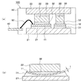
図1は、本発明の実施形態に係る半導体装置100の概略断面図であり、(a)は装置100の全体概略断面図、(b)は装置100の要部、すなわちIGBT素子11近傍の概略断面図である。なお、本実施形態では、ダイオード12についても図1(b)と同様の構成である。
1A and 1B are schematic cross-sectional views of a
図1に示されるように、本半導体装置100は、IGBT(Insulated Gate Bipolar Transistor)素子11と、ダイオード12とを備える。本実施形態では、これらIGBT素子11及びダイオード12が、ペアで回路を構成しており、本発明でいう半導体素子に相当する。
As shown in FIG. 1, the
ここにおいて、IGBT素子11およびダイオード12は、その厚さt(図1(b)参照)が150μm以下と薄いものである。そして、これら半導体素子11、12は、第1の導体部材としての第1のリード21の内面すなわち第1のリード21の上に搭載されている。
Here, the
この第1のリード21は、たとえば銅などの金属に代表される導電性材料よりなる板状のものである。図1(a)に示されるように、各半導体素子11、12と第1のリード21との間には、第1のはんだ31が介在しており、この第1のはんだ31を介して、各半導体素子11、12と第1のリード21とがはんだ接続されている。
The
また、各半導体素子11、12の上には、第2のはんだ32を介して、それぞれ第2の導体部材としてのターミナル22が搭載され、第2のはんだ32によりはんだ接続されている。
Further, on each
このターミナル22は、例えば銅などの金属に代表される導電性材料よりなるブロック状のものである。さらに、各ターミナル22の上には、第3のはんだ33を介して、例えば板状の銅などよりなる第2のリード23が接合されている。なお、本例では、第1のリード21は、IGBT素子のコレクタ側のリードであり、第2のリード22はエミッタ側のリードである。
The
ここで、本実施形態の半導体装置100において、第1のはんだ31の凝固点T1は第2のはんだ32の凝固点T2よりも低くなっており、さらに、第3のはんだ33の凝固点T3は、第1のはんだ31の凝固点T1および第2のはんだ32の凝固点T2よりも低いものとなっている。
Here, in the
つまり、第1のはんだ31の凝固点T1、第2のはんだ32の凝固点T2、第3のはんだ33の凝固点T3の間には、T2>T1>T3という凝固点の関係がある。これら各はんだ31〜33については、従来よりあるはんだ材料を採用でき、これらはんだ材料の中から当該凝固点の関係を満たすように、選択すればよい。なお、本実施形態の各はんだ31〜33の具体的な材質については、後述する。
That is, there is a relationship of freezing point T2> T1> T3 among the freezing point T1 of the
また、この半導体装置100においては、外部の部材と電気的に接続するための外部リード40が備えられており、この外部リード40とIGBT素子11とは、AuやAl等のボンディングワイヤ50により結線され、電気的に接続されている。
In addition, the
また、上記のように組み付けられた各部材11〜50は、例えばエポキシ樹脂等よりなるモールド樹脂60により、包み込まれるように封止されており、外部環境から保護されている。また、両リード21、23の外面は、モールド樹脂60より露出しており、放熱面となっている。
Moreover, each member 11-50 assembled | attached as mentioned above is sealed so that it may be wrapped with the
こうして、本半導体装置100では、両半導体素子11、12により回路が構成され、また、両リード21、23は電極としての機能も有する。従って、半導体素子11、12と外部との信号のやり取りは、各リード21、23、ボンディングワイヤ50及び外部リード40を介して行われる。
Thus, in this
また、両リード21、23は、半導体素子11、12の放熱を図る放熱部材としても機能し、例えば、図示しないが、両リード21、23の外面に、絶縁部材を介して冷却部材を配置する等により、放熱を促進するようになっている。
Both leads 21 and 23 also function as a heat radiating member for radiating heat from the
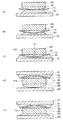
次に、本実施形態における半導体装置100の製造方法を説明する。図2(a)〜(e)は、本製造方法を上記図1に沿った断面にて示す工程図である。なお、図2では、半導体素子11、12のうちIGBT素子11を示しているが、ダイオード12についても同様である。
Next, a method for manufacturing the
まず、図2(a)に示されるように、第1のリード21の上に第1のはんだ31を介して半導体素子11、12を搭載し、この半導体素子11、12の上に第2のはんだ32を介してターミナル22を搭載する。ここで、各はんだ31、32としては、はんだ箔やはんだペーストなどを採用できる。
First, as shown in FIG. 2A, the
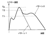
次に、このものを炉などに投入し、各はんだ31、32のリフローを行う。図3は、本製造方法に採用される、はんだリフロー工程における温度プロファイルの一例を示す図である。
Next, this is put into a furnace or the like, and reflow of each
このはんだリフロー工程では、まず、図3に示されるように、第1のはんだ31の凝固点T1および第2のはんだ32の凝固点T2よりも高い温度まで、温度を上昇させ、これら第1および第2のはんだ31、32をリフローさせ、液状とする。このときピーク温度をTpとする。このピーク温度Tpは、例えば、第2のはんだ32の凝固点T2よりも20〜60℃に設定することが望ましい。
In this solder reflow process, first, as shown in FIG. 3, the temperature is raised to a temperature higher than the freezing point T1 of the
次に、図3に示されるように、ピーク温度Tpから温度を降下させ、第2のはんだ32の凝固点T2よりも低く且つ第1のはんだ31の凝固点T1よりも高い状態とする。この状態において、図2(b)に示されるように、半導体素子11、12の上側に位置する第2のはんだ32が凝固し、半導体素子11、12とターミナル22とが第2のはんだ32を介して固着する。
Next, as shown in FIG. 3, the temperature is lowered from the peak temperature Tp so as to be lower than the freezing point T2 of the
次に、図3に示されるように、温度をさらに降下させ、第1のはんだ31の凝固点T1よりも低い状態とする。この状態において、図2(c)に示されるように、第2のはんだ32が凝固したままの状態で、半導体素子11、12の下側に位置する第1のはんだ31が凝固し、半導体素子11、12と第1のリード21とが第1のはんだ31を介して固着する。
Next, as shown in FIG. 3, the temperature is further lowered to a state lower than the freezing point T <b> 1 of the
また、図2(a)〜(c)に示されるように、当該はんだリフロー工程においては、上述したように、半導体素子11、12は、当該半導体素子11、12内のバイメタル効果により生じる熱応力により、反った状態となり、この状態で、上下の導体部材21、22とはんだ接続される。
Further, as shown in FIGS. 2A to 2C, in the solder reflow process, as described above, the
なお、図3では、ピーク温度Tpからの温度の下降パターンが破線の場合と実線の場合との2パターン示されているが、本実施形態においては、どちらのパターンを採用してもよい。ただし、実線で示されるパターン2のように、凝固点T2からその下の凝固点T1への降温速度が緩やかな方が好ましい。
In FIG. 3, two patterns of the temperature decrease pattern from the peak temperature Tp are shown, which are a broken line and a solid line, but either pattern may be employed in the present embodiment. However, it is preferable that the rate of temperature decrease from the freezing point T2 to the lower freezing point T1 is slow as in the
このようにして、図2(c)に示されるように、第1のリード21とターミナル22との間に半導体素子11、12がはんだ接続された状態で挟み込まれたワーク110ができあがる。
In this manner, as shown in FIG. 2C, a
続いて、図2(d)に示されるように、このワーク110を、ターミナル22側を下方に位置させた状態で、第3のはんだ33を介して、第3の導体部材としての第2のリード23の上に搭載する。この第3のはんだ33としても、はんだ箔やはんだペーストなどを採用できる。
Subsequently, as shown in FIG. 2 (d), the
次に、図2(e)に示されるように、第3のはんだ33をリフローさせることにより、ターミナル22と第2のリード23とを、第3のはんだ33を介して固着させる。こうして、ワーク110と第2のリード23とのはんだ接続が完了する。
Next, as shown in FIG. 2E, the terminal 22 and the
ここで、上述したように、第3のはんだ33の凝固点T3は、第1のはんだ31の凝固点T1および第2のはんだ32の凝固点T2よりも低いため、第3のはんだ33のリフロー温度は、当該第3のはんだ33の凝固点T3よりも高く且つ第1のはんだ31の凝固点T1よりも低い温度とする。
Here, as described above, since the freezing point T3 of the
それにより、第3のはんだ33のリフロー工程では、第1のはんだ31および第2のはんだ32は溶融せずに固着状態を維持したまま、第3のはんだ33によるリフロー・固着がなされる。
Thereby, in the reflow process of the
こうして、各導体部材21〜23および半導体素子11、12がこれら各部間に介在するはんだ31〜33を介して接合されたはんだ接合体ができあがる。続いて、本実施形態では、当該はんだ接合体を、モールド樹脂60にて封止することにより、上記図1に示される半導体装置100ができあがる。
Thus, a solder joined body is obtained in which the
なお、外部リード40とのボンディングワイヤ50による接続は、上記製造工程における適時に行えばよいが、例えば、上記ワーク110を形成した後であって第2のリード23とのはんだ接続を行う前に、当該ワーク110におけるIGBT素子11に対して行えばよい。
The connection with the
このように、本実施形態の半導体装置100は、第1のリード21の上に第1のはんだ31を介して半導体素子11、12を搭載し、この半導体素子11、12の上に第2のはんだ32を介してターミナル22を搭載した状態で、第1および第2のはんだ31、32をリフローさせることにより、半導体素子11、12とその上下の両導体部材21、22とをはんだ接続するようにしたものである。
As described above, the
そして、かかる半導体装置100においては、第2のはんだ32の凝固点T2が第1のはんだ31の凝固点T1よりも高いため、上記第1および第2のはんだ31、32の接合時に次のような作用が発揮される。
In the
上記製造方法の第1および第2のはんだ31、32の接合工程では、ピーク温度Tpにおいて、半導体素子11、12の反りが最も小さい状態にある。また、このピーク温度Tpにおいて、半導体素子11、12の上下に位置する第1および第2のはんだ31、32ともに液状である。
In the joining process of the first and
これを、高凝固点側である第2のはんだ32の凝固点T2まで下げることによって、半導体素子11、12の反りが小さい状態で、第2のはんだ32と半導体素子11、12とを固着させることできるため、従来に比べて、半導体素子11、12の反りを抑制することができる。
By lowering this to the freezing point T2 of the
さらに、上記図3において温度が凝固点T2と凝固点T1の間では、半導体素子11、12の反りが小さい状態を維持したまま、低凝固点側である第1のはんだ31の濡れを拡げることができる。
Furthermore, in FIG. 3, when the temperature is between the freezing point T2 and the freezing point T1, wetting of the
これは、半導体素子11、12と第2のはんだ32とターミナル22とが固着して一体化しているため、従来構造の第2のはんだ32に存在していた横方向へ分散する力F2(図9参照)をほぼゼロにすることが可能となることによる。
This is because the
そして、この効果により従来問題となっていた第2のはんだ32におけるスポンジ効果を無くすことができ、上側のターミナル22からの荷重F1は、第2のはんだ32にて分散されることなく、半導体素子11、12に加わる(図2(c)参照)。
This effect can eliminate the sponge effect in the
そのため、半導体素子11、12を押し下げ第1のはんだ31の濡れを押し進めようとする力が、従来に比べて弱まることなく、第1のはんだ31に加わる。その結果、第1のはんだ31と半導体素子11、12の端部との濡れ性を向上させることができる。
Therefore, the force that pushes down the
なお、これらのことから、上記図3において温度の下降パターンは、破線で示される急峻なパターン1よりも実線で示される緩やかなパターン2の方が好ましい。また、温度が凝固点T2と凝固点T1の間では、第1のはんだ31の濡れ性を拡げるような荷重を別途加えてもよい。
From these facts, the
また、本実施形態では、上述したように、ターミナル22と第2のリード23とを接続する第3のはんだ33の凝固点T3を、第1および第2のはんだ31、32の凝固点T1、T2よりも低いものとしているため、第1および第2のはんだ31、32を溶融させずに第3のはんだ33による固着がなされる。
In the present embodiment, as described above, the solidification point T3 of the
そのため、上記した効果、すなわち、第1のはんだ31および第2のはんだ32による半導体素子11、12の反りの抑制および第1のはんだ31の濡れの確保という効果を、維持したまま、つまり、第1および第2のはんだ31、32の形状を崩さずに、第3のはんだ33による接続が可能となる。
Therefore, the above-described effects, that is, the effects of suppressing warpage of the
本実施形態のように、第1のはんだ31の凝固点T1の方が第2のはんだ32の凝固点T2よりも低い構成とする場合、具体的に、各はんだ31、32の凝固点は、本半導体装置100に用いる半導体素子11、12に発生する反りの状態を考慮して設計する。この設計の一例について述べる。
When the freezing point T1 of the
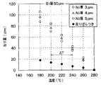
本発明者は、半導体素子としてのIGBT素子11についてFEM(有限要素法)解析を行い、当該IGBT素子11の温度とその反り量との関係を求めた。図4は、この解析に用いたIGBT素子11のモデルを示す図であり、(a)は当該モデルの斜視図、(b)は当該モデルの部分的な断面図である。
The inventor performed FEM (finite element method) analysis on the
IGBT素子11のモデルとしては、図4(a)に示されるように、表面積が□13mm×13mmの矩形状のモデルチップ11を用いた。このチップ11は、図4(b)に示されるように、一般的なIGBT素子11と同様に、Siよりなる基板11aの表面上にAlよりなる配線11b、さらに、その配線11bの上にNiよりなる電極11cが設けられた構成とした。
As a model of the
ここで、基板11aの厚さta(つまり、Si厚)は、50、100、150μmの3水準とし、配線11bの厚さtbは4μmとし、電極11cの厚さtcは3、4、5μmの3水準とし、IGBT素子11の温度を変えたときの当該素子の反り量を解析した。ここで、反り量は、最も反りの大きい素子端部におけるZ方向(素子の厚さt方向)の変位量である。
Here, the thickness ta (that is, Si thickness) of the
なお、ここでは、Alよりなる配線11bの塑性変形は無いものとし、Niよりなる電極11cとしては、一番応力がかかり反りが大きくなる純金属よりなるものを用いた場合として、解析を行った。また、基板11aの裏面電極は薄いため、その影響は実質的に無いものとした。
Here, it is assumed that there is no plastic deformation of the
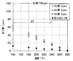
図5、図6、図7は、この図4に示されるモデルチップ11を用いた半導体素子11における温度と反り量との関係についての解析結果を示す図であり、それぞれ基板11aの厚さta(Si厚)としては、図5は50μmの場合、図6は100μmの場合、図7は150μmの場合を示す。
5, FIG. 6, and FIG. 7 are diagrams showing analysis results on the relationship between the temperature and the amount of warpage in the
ここで、反り量は、ピーク温度からの反り量の差である。また、図5〜図7においては、各温度にて各Ni電極11cの厚さ3μm、4μm、5μmに対する反り量が示されているが、この反り量とともに、各温度における各反り量の最大値と最小値との差を、反りばらつきとして示してある。 Here, the warpage amount is a difference in warpage amount from the peak temperature. 5 to 7 show the warpage amounts for the thicknesses of 3 μm, 4 μm, and 5 μm of each Ni electrode 11 c at each temperature. The maximum value of each warpage amount at each temperature is shown along with this warpage amount. And the minimum value are shown as warp variation.
図5〜図7からわかるように、280℃をピーク温度とした時、この280℃から温度を下げていくと、各材料の熱膨張係数差に準じ反り量が大きくなっていき、また、反りばらつきも大きくなっていく。また、実質的にIGBT素子11の厚さに相当する基板11aの厚さが150μmから、100μm、50μmと薄くなるにつれて、これら反り量および反りばらつきが大きくなっていく。
As can be seen from FIGS. 5 to 7, when the peak temperature is 280 ° C., when the temperature is lowered from 280 ° C., the amount of warpage increases according to the difference in thermal expansion coefficient of each material, and the warpage is increased. The variation also increases. Further, as the thickness of the
つまり、本発明者の検討によれば、半導体素子11、12の厚さが、少なくとも150μm以下の範囲は、その反りが問題となる程度の範囲にあるといえる。
In other words, according to the study by the present inventors, it can be said that the thickness of the
そして、図5〜図7に示されるように、基板11aの厚さが最も薄い50μmの場合において、反り量および反りばらつきともに最も大きく、IGBT素子11内に発生するバイメタル効果よる応力を最も受けることがわかる。
As shown in FIGS. 5 to 7, when the thickness of the
本実施形態の構造は、高凝固点側の第2のはんだ32を固着させることで半導体素子11、12の反りの抑制を行うが、この第2のはんだ32と低凝固点側の第1のはんだ31との凝固点の差が大きすぎると、半導体素子11、12に発生する熱応力が第2のはんだ32に加わって、はんだ剥れが生じたり、また、半導体素子11、12にかかる残留応力が大きくなるため、上記凝固点の差を限定する必要がある。
The structure of this embodiment suppresses the warpage of the
この図4に示されるようなモデルを用いた場合、半導体素子の温度間における反り量の差は、実用的には40μm以下が望ましい。また、反りばらつきについては、実用上、20μm以下が望ましい。これらの値は、たとえば製造上の歩留まり等を考慮して決められる仕様値である。 When a model as shown in FIG. 4 is used, the difference in warpage between the temperatures of the semiconductor elements is desirably 40 μm or less in practice. Further, it is desirable that the warpage variation is 20 μm or less in practice. These values are specification values determined in consideration of, for example, manufacturing yield.
このような仕様値を満足するという観点から、図5〜図7の各図において、第1および第2のはんだ31、32の両凝固点T1、T2の差に相当する望ましい温度範囲の一例をΔTとして示してある。もちろん、これらの温度範囲ΔTは一例であり、上記温度間での反り量の差が40μm以下、反りばらつきが20μm以下ならば、これに限定されるものではない。
From the viewpoint of satisfying such a specification value, an example of a desirable temperature range corresponding to the difference between the freezing points T1 and T2 of the first and
図5〜図7に示されているΔTの例に基づいて述べると、仮に240℃に凝固点があるはんだ材を、高凝固点側の第2のはんだ32として用いる場合には、低凝固点側の第1のはんだ31は、基板11aの厚さが50μmでは、200℃までの凝固点を持つものを用い(図5参照)、基板11aの厚さが100μmでは、180℃までの凝固点を持つものを用い(図6参照)、基板11aの厚さが150μmでは、140℃までの凝固点を持つものを用いればよい(図7参照)。
Referring to the example of ΔT shown in FIGS. 5 to 7, if a solder material having a freezing point at 240 ° C. is used as the
そして、この範囲内において、第1のはんだ31として、極力低い凝固点のものを選ぶことで、本実施形態の効果がよりよく得られる。このようにして、本実施形態では、半導体素子11、12の反り量を考慮して、第1のはんだ31および第2のはんだ32を選定する。
In this range, the effect of the present embodiment can be better obtained by selecting the
本実施形態における上記はんだ31、32を選定するうえでの具体的なはんだ材を、以下に示す。共晶ハンダとしては、Snを主成分としてAg、Cu、Ni、In、Bi、Sb、Au、Pb、Znなどを混ぜ合わせたものがあるが、代表例として以下のようなものが挙げられる。凝固点毎に分類して示す。
Specific solder materials for selecting the
280℃帯:Auを主成分としたもの。例えば、SnAu80など。 280 ° C. band: Au as a main component. For example, SnAu80.
230℃帯:Sbなどを織り交ぜたもの。例えば、SnCu2.0Sb0.8Ag0.2、SnSb5、Sn、SnCu0.7など。 230 ° C band: Interwoven with Sb. For example, SnCu2.0Sb0.8Ag0.2, SnSb5, Sn, SnCu0.7, etc.
220℃帯:SnAgCu組成を元にするもの。例えば、SnAg2.5Cu0.8Sb0.5、SnAg4.0Cu0.5、SnAg3.9Cu0.6、SnAg3.5、SnAg2.5Bi1.0Cu0.5、SnAg3.0Cu0.5、SnAg3.8Cu0.7、SnAg3.5Cu0.7、SnAg2.0Bi3.0Cu0.75、SnAg3.5Cu0.9など。 220 ° C. band: Based on SnAgCu composition. For example, SnAg2.5Cu0.8Sb0.5, SnAg4.0Cu0.5, SnAg3.9Cu0.6, SnAg3.5, SnAg2.5Bi1.0Cu0.5, SnAg3.0Cu0.5, SnAg3.8Cu0.7, SnAg3.5Cu0. 7, SnAg2.0Bi3.0Cu0.75, SnAg3.5Cu0.9, etc.
210℃帯:SnAgベースにIn、Biを混ぜたもの。例えば、SnIn4.0Ag3.5Bi0.5、SnAg3.4Bi4.8、SnBi7.5Ag2.0など。 210 ° C. band: SnAg base mixed with In and Bi. For example, SnIn4.0Ag3.5Bi0.5, SnAg3.4Bi4.8, SnBi7.5Ag2.0, etc.
200℃帯:SnAgベースにIn、Bi、Znを混ぜたもの。例えば、SnIn8.0Ag3.5Bi0.5、SnZn9 SnZn8Bi3など。 200 ° C. band: SnAg base mixed with In, Bi, Zn. For example, SnIn8.0Ag3.5Bi0.5, SnZn9 SnZn8Bi3, etc.
180℃帯:SnAgベースに多量のInを混ぜたもの。例えば、SnIn20Ag2.8や従来のSnPb37など。 180 ° C. band: SnAg base mixed with a large amount of In. For example, SnIn20Ag2.8 or conventional SnPb37.
140℃帯:Snベースに多量のBiを混ぜたもの。例えば、SnBi57Ag1、SnBi58など。 140 ° C. band: Sn base mixed with a large amount of Bi. For example, SnBi57Ag1 and SnBi58.
また、共晶はんだでなくとも、その組成を変えたα固溶体、β固溶体を用いたときその粘度から半導体素子11、12の反り抑制に同様の効果を得られるものであればそれでもよい。
Moreover, even if it is not a eutectic solder, when the (alpha) solid solution and (beta) solid solution which changed the composition are used, if the same effect can be obtained from the viscosity to the curvature suppression of the
(他の実施形態)
図8(a)は、本発明の他の実施形態にかかる半導体装置の要部の概略断面構成を示す図であり、図8(b)は(a)に示される構成の形成方法を示す概略断面図である。なお、この図8(a)において、図示しない部分は上記第1実施形態の半導体装置と同様である。
(Other embodiments)
FIG. 8A is a diagram showing a schematic cross-sectional configuration of a main part of a semiconductor device according to another embodiment of the present invention, and FIG. 8B is a schematic diagram showing a method for forming the configuration shown in FIG. It is sectional drawing. In FIG. 8A, the portions not shown are the same as those of the semiconductor device of the first embodiment.
図8(a)に示されるように、第1の導体部材である第1のリード21の上面のうちIGBT素子11の端部が重なる部位に、突起21aを設ける。なお、この突起21aは、ダイオード12側の部位についても同様に設けてよい。
As shown in FIG. 8A, a
この突起21aは、図8(b)に示されるように、第1のリード21の上面のうちIGBT素子11の端部が重なる部位に、治具Kによりプレス加工を行うことにより形成することができる。
As shown in FIG. 8B, the
このプレス加工により、溝部21bが形成されるとともに、溝部21bを挟んで左右に突起が発生し、一方の突起21aがIGBT素子11の端部が重なる部位に位置するようにする。
By this press working, the
この突起21aによれば、第1のリード21の上に第1のはんだ31を配設したときに、この突起21aによって第1のはんだ31が盛り上がった状態となる。そのため、IGBT素子11の端部に位置する第1のはんだ31の厚みを稼ぐことができ、IGBT素子11と第1のはんだ31との濡れ性の向上が期待できる。
According to the
また、図8の場合、はんだ接合時には、第1のはんだ31のうちの過剰分は、溝部21bに吸収されて、それ以上濡れ広がるのを抑制できるため、過剰なはんだがIGBT素子11の上面まで回り込んで短絡などを引き起こすのを防止できる。
Further, in the case of FIG. 8, at the time of solder joining, an excess amount of the
ここで、突起21aの高さh(図8(b)参照)は、IGBT素子11の反り量と同等以下が望ましく、溝部21bの長さは、IGBT素子11の反りばらつきにより想定される過剰ハンダ量を考慮して求めればよい。
Here, the height h of the
また、上記実施形態では、IGBT素子11とダイオード12の両方について、上記図1(b)に示したような、はんだ31、32の構成を採用したが、IGBT素子11のみ、またはダイオード12のみが上記のはんだ構成でもよい。
Moreover, in the said embodiment, although the structure of the
また、上記実施形態では、半導体素子は複数個設けられたものであったが、複数個の場合、上記したIGBT素子とダイオードとの組合せに限定されるものではなく、例えばパワートランジスタ素子であってもよい。また、半導体素子は複数個ではなく、1個であってもよい。 In the above embodiment, a plurality of semiconductor elements are provided. However, in the case of a plurality of semiconductor elements, the combination is not limited to the above-described IGBT element and diode. Also good. Further, the number of semiconductor elements is not limited to one but may be one.
さらに、上記実施形態では、半導体装置はモールド樹脂60で封止されていたが、モールド樹脂で封止されていないものでもよい。具体的には、上記図1(a)においてモールド樹脂60を省略した構成のものであってもよい。
Furthermore, in the said embodiment, although the semiconductor device was sealed with the
また、半導体装置としては、第1の導体部材と第2の導体部材との間に半導体素子を挟み込み、半導体素子とその上下の導体部材とをはんだ接続してなるものであればよく、さらに第3の導体部材および第3のはんだがないものであってもよい。 The semiconductor device may be any device as long as the semiconductor element is sandwiched between the first conductor member and the second conductor member, and the semiconductor element and the upper and lower conductor members are connected by soldering. There may be no conductor member 3 and no third solder.
例えば、上記図1(a)において、ターミナル22および第3のはんだ33を省略し、半導体素子11、12を第2のはんだ32を介して直接、第2のリード23に接続してもよく、この場合には、第2のリード23が第2の導体部材として構成される。
For example, in FIG. 1A, the terminal 22 and the
11…半導体素子としてのIGBT素子、12…半導体素子としてのダイオード、
21…第1の導体部材としての第1のリード、21a…突起、
22…第2の導体部材としてのターミナル、
23…第3の導体部材としての第3のリード、
31…第1のはんだ、32…第2のはんだ、33…第3のはんだ。
11 ... IGBT element as a semiconductor element, 12 ... Diode as a semiconductor element,
21 ... 1st lead as 1st conductor member, 21a ... Projection,
22: Terminal as a second conductor member,
23 ... a third lead as a third conductor member,
31 ... 1st solder, 32 ... 2nd solder, 33 ... 3rd solder.
Claims (4)
前記第1のはんだ(31)の凝固点が、前記第2のはんだ(32)の凝固点よりも低いことを特徴とする半導体装置。 The semiconductor element (11, 12) is mounted on the first conductor member (21) via the first solder (31), and the second solder (32) is mounted on the semiconductor element (11, 12). In a state where the second conductor member (22) is mounted via the first and second solders (31, 32), the semiconductor element (11, 12) and the both conductor members ( 21 and 22) in a semiconductor device in which solder connection is made,
A semiconductor device, wherein a freezing point of the first solder (31) is lower than a freezing point of the second solder (32).
前記第3のはんだ(33)の凝固点は、前記第1のはんだ(31)の凝固点および前記第2のはんだ(32)の凝固点よりも低いことを特徴とする請求項1または2に記載の半導体装置。 A third conductor member (23) is solder-connected to the second conductor member (22) via a third solder (33);
3. The semiconductor according to claim 1, wherein the freezing point of the third solder (33) is lower than the freezing point of the first solder (31) and the freezing point of the second solder (32). apparatus.
Priority Applications (1)
| Application Number | Priority Date | Filing Date | Title |
|---|---|---|---|
| JP2006107161A JP4730181B2 (en) | 2006-04-10 | 2006-04-10 | Semiconductor device |
Applications Claiming Priority (1)
| Application Number | Priority Date | Filing Date | Title |
|---|---|---|---|
| JP2006107161A JP4730181B2 (en) | 2006-04-10 | 2006-04-10 | Semiconductor device |
Publications (2)
| Publication Number | Publication Date |
|---|---|
| JP2007281274A true JP2007281274A (en) | 2007-10-25 |
| JP4730181B2 JP4730181B2 (en) | 2011-07-20 |
Family
ID=38682405
Family Applications (1)
| Application Number | Title | Priority Date | Filing Date |
|---|---|---|---|
| JP2006107161A Expired - Fee Related JP4730181B2 (en) | 2006-04-10 | 2006-04-10 | Semiconductor device |
Country Status (1)
| Country | Link |
|---|---|
| JP (1) | JP4730181B2 (en) |
Cited By (8)
| Publication number | Priority date | Publication date | Assignee | Title |
|---|---|---|---|---|
| WO2010004609A1 (en) * | 2008-07-07 | 2010-01-14 | 三菱電機株式会社 | Power semiconductor device |
| DE102009040444A1 (en) | 2009-03-23 | 2010-10-07 | Mitsubishi Electric Corp. | power module |
| JP2014135527A (en) * | 2014-04-30 | 2014-07-24 | Rohm Co Ltd | Semiconductor power module and method for manufacturing the same |
| US8981542B2 (en) | 2010-09-29 | 2015-03-17 | Rohm Co., Ltd. | Semiconductor power module and method of manufacturing the same |
| JP2015095561A (en) * | 2013-11-12 | 2015-05-18 | 株式会社デンソー | Semiconductor device and manufacturing method of the same |
| EP3063697A1 (en) * | 2013-10-30 | 2016-09-07 | Ingenico Group | Support entering into the fabrication of an electronic device, memory card connector, memory card reading terminal and method of fabrication corresponding thereto |
| JP2016219479A (en) * | 2015-05-15 | 2016-12-22 | トヨタ自動車株式会社 | Manufacturing method for semiconductor device, and semiconductor device |
| JP2018148169A (en) * | 2017-03-09 | 2018-09-20 | トヨタ自動車株式会社 | Semiconductor device |
Families Citing this family (2)
| Publication number | Priority date | Publication date | Assignee | Title |
|---|---|---|---|---|
| JP6750263B2 (en) | 2016-03-18 | 2020-09-02 | 富士電機株式会社 | Power semiconductor module |
| JP7027751B2 (en) | 2017-09-15 | 2022-03-02 | 富士電機株式会社 | Semiconductor module |
Citations (3)
| Publication number | Priority date | Publication date | Assignee | Title |
|---|---|---|---|---|
| JPS52127160A (en) * | 1976-04-19 | 1977-10-25 | Toshiba Corp | Semiconductor device |
| JPH08139243A (en) * | 1994-11-07 | 1996-05-31 | Rohm Co Ltd | Manufacture of semiconductor device |
| JP2001274177A (en) * | 2000-03-24 | 2001-10-05 | Denso Corp | Semiconductor device and method of manufacturing the same |
-
2006
- 2006-04-10 JP JP2006107161A patent/JP4730181B2/en not_active Expired - Fee Related
Patent Citations (3)
| Publication number | Priority date | Publication date | Assignee | Title |
|---|---|---|---|---|
| JPS52127160A (en) * | 1976-04-19 | 1977-10-25 | Toshiba Corp | Semiconductor device |
| JPH08139243A (en) * | 1994-11-07 | 1996-05-31 | Rohm Co Ltd | Manufacture of semiconductor device |
| JP2001274177A (en) * | 2000-03-24 | 2001-10-05 | Denso Corp | Semiconductor device and method of manufacturing the same |
Cited By (12)
| Publication number | Priority date | Publication date | Assignee | Title |
|---|---|---|---|---|
| WO2010004609A1 (en) * | 2008-07-07 | 2010-01-14 | 三菱電機株式会社 | Power semiconductor device |
| JPWO2010004609A1 (en) * | 2008-07-07 | 2011-12-22 | 三菱電機株式会社 | Power semiconductor device |
| DE102009040444A1 (en) | 2009-03-23 | 2010-10-07 | Mitsubishi Electric Corp. | power module |
| US7848104B2 (en) | 2009-03-23 | 2010-12-07 | Mitsubishi Electric Corporation | Power module |
| DE102009040444B4 (en) * | 2009-03-23 | 2012-11-08 | Mitsubishi Electric Corp. | power module |
| US8981542B2 (en) | 2010-09-29 | 2015-03-17 | Rohm Co., Ltd. | Semiconductor power module and method of manufacturing the same |
| EP3063697A1 (en) * | 2013-10-30 | 2016-09-07 | Ingenico Group | Support entering into the fabrication of an electronic device, memory card connector, memory card reading terminal and method of fabrication corresponding thereto |
| EP3063697B1 (en) * | 2013-10-30 | 2022-04-06 | Banks and Acquirers International Holding | Memory card reading assembly including anti-intrusion protection |
| JP2015095561A (en) * | 2013-11-12 | 2015-05-18 | 株式会社デンソー | Semiconductor device and manufacturing method of the same |
| JP2014135527A (en) * | 2014-04-30 | 2014-07-24 | Rohm Co Ltd | Semiconductor power module and method for manufacturing the same |
| JP2016219479A (en) * | 2015-05-15 | 2016-12-22 | トヨタ自動車株式会社 | Manufacturing method for semiconductor device, and semiconductor device |
| JP2018148169A (en) * | 2017-03-09 | 2018-09-20 | トヨタ自動車株式会社 | Semiconductor device |
Also Published As
| Publication number | Publication date |
|---|---|
| JP4730181B2 (en) | 2011-07-20 |
Similar Documents
| Publication | Publication Date | Title |
|---|---|---|
| JP4730181B2 (en) | Semiconductor device | |
| JP4302607B2 (en) | Semiconductor device | |
| CN109314063B (en) | Power semiconductor device | |
| JP6206494B2 (en) | Semiconductor device | |
| US11071212B2 (en) | Semiconductor device manufacturing method | |
| US11164846B2 (en) | Semiconductor device manufacturing method and soldering support jig | |
| JP6448418B2 (en) | Power semiconductor device | |
| JP5732880B2 (en) | Semiconductor device and manufacturing method thereof | |
| JP4228926B2 (en) | Semiconductor device | |
| JP6008750B2 (en) | Semiconductor device | |
| JP2005340268A (en) | Transistor package | |
| JP5774292B2 (en) | Circuit device and manufacturing method thereof | |
| JP2009147123A (en) | Semiconductor device, and manufacturing method therefor | |
| JPWO2019116910A1 (en) | Semiconductor devices and methods for manufacturing semiconductor devices | |
| JP4882394B2 (en) | Semiconductor device | |
| JP6477105B2 (en) | Semiconductor device | |
| JP7347047B2 (en) | semiconductor equipment | |
| JP4214880B2 (en) | Semiconductor device | |
| JP4861200B2 (en) | Power module | |
| JP2008270846A (en) | Method for manufacturing semiconductor device | |
| WO2021220357A1 (en) | Semiconductor device | |
| US20220148944A1 (en) | Electronic device and method for manufacturing electronic device | |
| WO2021240944A1 (en) | Semiconductor device | |
| JP2009105327A (en) | Semiconductor device with heat sink and its method for manufacturing | |
| JP2016030281A (en) | Junction material and semiconductor device |
Legal Events
| Date | Code | Title | Description |
|---|---|---|---|
| A621 | Written request for application examination |
Free format text: JAPANESE INTERMEDIATE CODE: A621 Effective date: 20080512 |
|
| A977 | Report on retrieval |
Free format text: JAPANESE INTERMEDIATE CODE: A971007 Effective date: 20101224 |
|
| A131 | Notification of reasons for refusal |
Free format text: JAPANESE INTERMEDIATE CODE: A131 Effective date: 20110111 |
|
| A521 | Request for written amendment filed |
Free format text: JAPANESE INTERMEDIATE CODE: A523 Effective date: 20110301 |
|
| TRDD | Decision of grant or rejection written | ||
| A01 | Written decision to grant a patent or to grant a registration (utility model) |
Free format text: JAPANESE INTERMEDIATE CODE: A01 Effective date: 20110322 |
|
| A61 | First payment of annual fees (during grant procedure) |
Free format text: JAPANESE INTERMEDIATE CODE: A61 Effective date: 20110404 |
|
| FPAY | Renewal fee payment (event date is renewal date of database) |
Free format text: PAYMENT UNTIL: 20140428 Year of fee payment: 3 |
|
| R151 | Written notification of patent or utility model registration |
Ref document number: 4730181 Country of ref document: JP Free format text: JAPANESE INTERMEDIATE CODE: R151 |
|
| FPAY | Renewal fee payment (event date is renewal date of database) |
Free format text: PAYMENT UNTIL: 20140428 Year of fee payment: 3 |
|
| R250 | Receipt of annual fees |
Free format text: JAPANESE INTERMEDIATE CODE: R250 |
|
| R250 | Receipt of annual fees |
Free format text: JAPANESE INTERMEDIATE CODE: R250 |
|
| R250 | Receipt of annual fees |
Free format text: JAPANESE INTERMEDIATE CODE: R250 |
|
| R250 | Receipt of annual fees |
Free format text: JAPANESE INTERMEDIATE CODE: R250 |
|
| R250 | Receipt of annual fees |
Free format text: JAPANESE INTERMEDIATE CODE: R250 |
|
| R250 | Receipt of annual fees |
Free format text: JAPANESE INTERMEDIATE CODE: R250 |
|
| R250 | Receipt of annual fees |
Free format text: JAPANESE INTERMEDIATE CODE: R250 |
|
| R250 | Receipt of annual fees |
Free format text: JAPANESE INTERMEDIATE CODE: R250 |
|
| LAPS | Cancellation because of no payment of annual fees |