JP2007281237A - Method for manufacturing solid electrolytic capacitor - Google Patents
Method for manufacturing solid electrolytic capacitor Download PDFInfo
- Publication number
- JP2007281237A JP2007281237A JP2006106244A JP2006106244A JP2007281237A JP 2007281237 A JP2007281237 A JP 2007281237A JP 2006106244 A JP2006106244 A JP 2006106244A JP 2006106244 A JP2006106244 A JP 2006106244A JP 2007281237 A JP2007281237 A JP 2007281237A
- Authority
- JP
- Japan
- Prior art keywords
- lead terminal
- terminal
- anode
- solid electrolytic
- capacitor element
- Prior art date
- Legal status (The legal status is an assumption and is not a legal conclusion. Google has not performed a legal analysis and makes no representation as to the accuracy of the status listed.)
- Pending
Links
- 239000003990 capacitor Substances 0.000 title claims abstract description 43
- 239000007787 solid Substances 0.000 title claims abstract description 27
- 238000004519 manufacturing process Methods 0.000 title claims abstract description 7
- 238000000034 method Methods 0.000 title abstract description 11
- 239000011104 metalized film Substances 0.000 claims abstract description 17
- 229920005989 resin Polymers 0.000 claims abstract description 15
- 239000011347 resin Substances 0.000 claims abstract description 15
- 230000032683 aging Effects 0.000 claims description 19
- 238000005452 bending Methods 0.000 claims description 7
- 238000007789 sealing Methods 0.000 claims description 3
- 230000003679 aging effect Effects 0.000 abstract description 2
- BQCADISMDOOEFD-UHFFFAOYSA-N Silver Chemical compound [Ag] BQCADISMDOOEFD-UHFFFAOYSA-N 0.000 description 6
- 229910052709 silver Inorganic materials 0.000 description 6
- 239000004332 silver Substances 0.000 description 6
- NBIIXXVUZAFLBC-UHFFFAOYSA-N Phosphoric acid Chemical compound OP(O)(O)=O NBIIXXVUZAFLBC-UHFFFAOYSA-N 0.000 description 4
- 239000010408 film Substances 0.000 description 4
- OKTJSMMVPCPJKN-UHFFFAOYSA-N Carbon Chemical compound [C] OKTJSMMVPCPJKN-UHFFFAOYSA-N 0.000 description 3
- 229910052799 carbon Inorganic materials 0.000 description 3
- GUVRBAGPIYLISA-UHFFFAOYSA-N tantalum atom Chemical compound [Ta] GUVRBAGPIYLISA-UHFFFAOYSA-N 0.000 description 3
- 239000000853 adhesive Substances 0.000 description 2
- 230000001070 adhesive effect Effects 0.000 description 2
- 229910000147 aluminium phosphate Inorganic materials 0.000 description 2
- 239000007864 aqueous solution Substances 0.000 description 2
- 230000007547 defect Effects 0.000 description 2
- NUJOXMJBOLGQSY-UHFFFAOYSA-N manganese dioxide Chemical compound O=[Mn]=O NUJOXMJBOLGQSY-UHFFFAOYSA-N 0.000 description 2
- 229910052751 metal Inorganic materials 0.000 description 2
- 239000002184 metal Substances 0.000 description 2
- 239000007784 solid electrolyte Substances 0.000 description 2
- 125000006850 spacer group Chemical group 0.000 description 2
- 229910052782 aluminium Inorganic materials 0.000 description 1
- XAGFODPZIPBFFR-UHFFFAOYSA-N aluminium Chemical compound [Al] XAGFODPZIPBFFR-UHFFFAOYSA-N 0.000 description 1
- 230000000052 comparative effect Effects 0.000 description 1
- 229920001940 conductive polymer Polymers 0.000 description 1
- 230000006378 damage Effects 0.000 description 1
- 230000002950 deficient Effects 0.000 description 1
- 239000003792 electrolyte Substances 0.000 description 1
- 239000003822 epoxy resin Substances 0.000 description 1
- MIVBAHRSNUNMPP-UHFFFAOYSA-N manganese(2+);dinitrate Chemical compound [Mn+2].[O-][N+]([O-])=O.[O-][N+]([O-])=O MIVBAHRSNUNMPP-UHFFFAOYSA-N 0.000 description 1
- 238000000465 moulding Methods 0.000 description 1
- 229920000647 polyepoxide Polymers 0.000 description 1
- 229920006267 polyester film Polymers 0.000 description 1
- 238000003825 pressing Methods 0.000 description 1
- 239000000243 solution Substances 0.000 description 1
- 238000005979 thermal decomposition reaction Methods 0.000 description 1
- 229920001187 thermosetting polymer Polymers 0.000 description 1
- 239000010409 thin film Substances 0.000 description 1
- 238000007740 vapor deposition Methods 0.000 description 1
- 238000003466 welding Methods 0.000 description 1
Images
Landscapes
- Fixed Capacitors And Capacitor Manufacturing Machines (AREA)
Abstract
Description
本発明は、固体電解コンデンサの製造方法に関し、詳しくは、そのエージング方法に関するものである。 The present invention relates to a method of manufacturing a solid electrolytic capacitor, and more particularly to an aging method thereof.
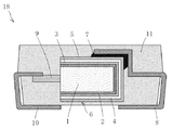
従来、固体電解コンデンサは、図1に示すように、陽極ワイヤ9が突出して設けられた弁作用金属からなる陽極体1の表面に、酸化皮膜層2、二酸化マンガンや導電性高分子等の固体電解質層3、カーボン層4および銀層5を順次形成してコンデンサ素子6とし、舌状の陽極リード端子10および陰極リード端子8それぞれの一端に対して陽極ワイヤ9および銀層5をそれぞれ接続し、さらに、コンデンサ素子6および両リード端子8、10の基端側を外装樹脂11にて封止した後、外装樹脂11から突出している両リード端子8、10を、それぞれ所定形状に折り曲げて製品形状としている。
Conventionally, as shown in FIG. 1, a solid electrolytic capacitor has a solid body such as an
上記のような固体電解コンデンサ18を製造する際は、一般に、外装樹脂11で封止した後に両リード端子8、10を折り曲げる前の状態(図2A参照)において、当該固体電解コンデンサを恒温槽内に長時間さらすと共に両リード端子8、10間に所定電圧を印加することにより、製品組み立て時に生じた酸化皮膜層2の部分的破壊を修復するエージング処理が行われている。
When manufacturing the solid
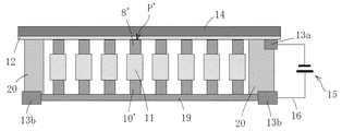
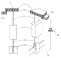
このエージング処理は、図5および図6に示す如く、複数の固体電解コンデンサの一方のリード端子10’がそれぞれ連結された共通の導電性フレーム19に対して給電端子13bを接続すると共に、他方の給電端子13aが接続されたメタライズドフィルム(金属化フィルム)12を、他方のリード端子8’における先端の面P’に対し、スポンジ等の押え部材14により当該リード端子の突出方向に沿って押し付け、さらに、給電端子13aおよび13b間に電源15から給電用電線16を介して電圧を印加することにより、行われていた。
このエージング方法によれば、一度に多数個の固体電解コンデンサに電圧印加が可能であり、さらに、いずれかの固体電解コンデンサに短絡が生じたとき、当該固体電解コンデンサに当接するメタライズドフィルム12の蒸着金属薄膜がその短絡エネルギーで蒸発飛散して電気的接続が絶たれるため、短絡していない他の正常な固体電解コンデンサに影響を与えたり、給電用端子13a、13b等の給電装置を焼損したりすることなく、エージングを行うことができる(例えば、特許文献1参照)。
According to this aging method, it is possible to apply a voltage to a large number of solid electrolytic capacitors at a time, and when a short circuit occurs in any of the solid electrolytic capacitors, vapor deposition of the
しかし、上記のような方法では、図5および図6に示す如く、リード端子8’における先端の面P’がメタライズドフィルム12に当接しているのみであり、接触面積が小さいため接触不良を生じてエージングが不十分となり、固体電解コンデンサの漏れ電流特性が悪化するという問題があった。
However, in the method as described above, as shown in FIGS. 5 and 6, the tip surface P ′ of the
本発明は、このような従来の問題点を解決するもので、一度に多数個の固体電解コンデンサに電圧印加が可能であり、かつ、安定したエージング効果が得られる固体電解コンデンサの製造方法を提供するものである。 The present invention solves such a conventional problem, and provides a method of manufacturing a solid electrolytic capacitor that can apply a voltage to a large number of solid electrolytic capacitors at a time and can provide a stable aging effect. To do.
上記課題を解決するために本発明は、一方側に陽極部、他方側に陰極部を有するコンデンサ素子を作製する工程と、前記コンデンサ素子の陽極部および陰極部に対し、陽極リード端子および陰極リード端子を、互いに反対方向を向いて外方へ突出するようにそれぞれ接続する工程と、前記コンデンサ素子ならびに前記陽極リード端子および陰極リード端子の基端側を外装樹脂で封止する工程と、前記外装樹脂から突出している前記陽極リード端子および陰極リード端子の少なくとも一方を、突出方向に略垂直な平面を有する所定形状に折り曲げる工程と、前記平面に対し、第1の給電端子に接続されたメタライズドフィルムを当接させると共に、他方のリード端子に対し第2の給電端子を接続し、当該第1および第2の給電端子間に所定電圧を印加して前記コンデンサ素子をエージングする工程と、を有することを特徴とする固体電解コンデンサの製造方法を提供するものである。 In order to solve the above problems, the present invention provides a process for producing a capacitor element having an anode part on one side and a cathode part on the other side, and an anode lead terminal and a cathode lead for the anode part and the cathode part of the capacitor element. A step of connecting the terminals so as to protrude outward in opposite directions, a step of sealing the base end side of the capacitor element and the anode lead terminal and the cathode lead terminal with an exterior resin, and the exterior Bending at least one of the anode lead terminal and the cathode lead terminal protruding from the resin into a predetermined shape having a plane substantially perpendicular to the protruding direction, and a metallized film connected to the first power supply terminal with respect to the plane And the second lead terminal is connected to the other lead terminal, and a predetermined voltage is applied between the first and second feed terminals. A step of aging the capacitor element is applied to, there is provided a method of manufacturing a solid electrolytic capacitor characterized by having a.
本発明によれば、外装樹脂から突出している陽極リード端子および陰極リード端子の少なくとも一方を、突出方向に略垂直な平面を有する所定形状に折り曲げた後に、当該平面にメタライズドフィルムを十分に当接させてエージングするため、接触不良によるエージング不足を低減し、固体電解コンデンサの漏れ電流不良を低減することができる。 According to the present invention, after bending at least one of the anode lead terminal and the cathode lead terminal protruding from the exterior resin into a predetermined shape having a plane substantially perpendicular to the protruding direction, the metallized film is sufficiently brought into contact with the plane. Therefore, the aging shortage due to the contact failure can be reduced, and the leakage current failure of the solid electrolytic capacitor can be reduced.
以下、図面を参照しつつ本発明の実施例について説明し、これらの特性と比較例の特性とを比較検討する。 Hereinafter, embodiments of the present invention will be described with reference to the drawings, and these characteristics and characteristics of comparative examples will be compared and examined.
[実施例]
まず、タンタル粉末にタンタルワイヤ(陽極ワイヤ)9の一部を埋め込んだものを加圧成形し、これを真空焼結することによって陽極体1(図1参照)を形成した。
次いで、リン酸0.1%水溶液槽(不図示)に陽極体1を浸け、陽極体1を陽極、当該リン酸水溶液槽を陰極として両極間に20V印加し、陽極体1の表面に酸化皮膜層2(図1参照)を形成した。
次いで、陽極体1を硝酸マンガン溶液に浸漬し、熱分解処理することにより固体電解質層3を形成し、さらに、カーボン層4、銀層5を順次設け、コンデンサ素子6を作製した(図1参照)。
[Example]
First, a tantalum powder in which a part of a tantalum wire (anode wire) 9 was embedded was pressure-molded, and this was vacuum sintered to form an anode body 1 (see FIG. 1).
Next, the
Next, the
次に、コンデンサ素子6の銀層5と陰極リード端子8とを、銀を含む導電性接着剤7により接続すると共に、陽極ワイヤ9と陽極リード端子10とを、突き合わせて抵抗溶接により接続した(図1参照)。
Next, the
次に、熱硬化性のエポキシ樹脂を用いたモールド成形により、図2Aに示す如く、コンデンサ素子6、陽極リード10および陰極リード8を封止する外装樹脂11を形成した。
Next, as shown in FIG. 2A, an
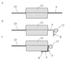
次に、図2Bに示す如く、外装樹脂11から突出する陰極リード端子8の先端部分をフォーミングローラ17により下方に向けて折り曲げた後、図2Cに示す如く、陰極リード端子8を外装樹脂11との境界付近から下方に向けて折り曲げ、全体が外装樹脂11の形状に沿うような所定形状にした。このとき、陰極リード端子8には、図2Cに示す如く、当該リード端子の突出方向に略垂直な平面Pが形成される。
Next, as shown in FIG. 2B, the tip portion of the
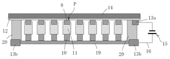
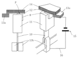
その後、図3および図4に示すように、陽極リード端子10を、導電性フレーム19を介して給電端子13bに接続すると共に、給電端子13aに接続された厚さ11.9μmのメタライズドフィルム12を、スポンジ14により陰極リード端子8の平面Pに押し付けて当接させ、さらに、130℃の恒温槽内において、電圧供給用の電源15から給電用電線16を介して給電端子13a、13b間に10V印加し、2時間かけてエージングを行った。なお、メタライズドフィルム12と、給電端子13bおよび導電性フレーム19とは、絶縁用スペーサ20によって絶縁されている。
また、メタライズドフィルムは、ポリエステルフィルム上にアルミニウムを蒸着したものを用いた。
Thereafter, as shown in FIGS. 3 and 4, the
Moreover, the metallized film used what vapor-deposited aluminum on the polyester film.
そして、陰極リード端子8と同様に、陽極リード端子10をフォーミングローラ17によって所定形状に折り曲げ、2.0mm×1.25mm×1.1mm寸法で定格が10V−10μFである固体電解コンデンサ18(図1参照)を10,000個作製した。
Then, similarly to the
[従来例]
次に、図5および図6に示すように、所定形状に折り曲げる前の陰極リード端子8’における先端の面P’をメタライズドフィルム12に当接させてエージングを行い、その後、陰極リード端子8’および陽極リード端子10’を所定形状に折り曲げて形成した以外は、実施例と同様の方法で、固体電解コンデンサ18(図1参照)を10,000個作製した。
[Conventional example]
Next, as shown in FIGS. 5 and 6, aging is performed by bringing the tip surface P ′ of the
実施例および従来例にかかる固体電解コンデンサについて、漏れ電流値、漏れ電流不良率を測定した結果を表1に示す。なお、漏れ電流値は、直流電圧10Vを1分間印加した後の漏れ電流値の平均値とし、漏れ電流不良率は、直流電圧10Vを1分間印加した後の漏れ電流値が1μA以上となった製品を不良として算出した。 Table 1 shows the results of measuring the leakage current value and the leakage current defect rate for the solid electrolytic capacitors according to the example and the conventional example. The leakage current value is the average value of the leakage current value after applying a DC voltage of 10 V for 1 minute, and the leakage current failure rate is 1 μA or more after applying the DC voltage of 10 V for 1 minute. The product was calculated as defective.
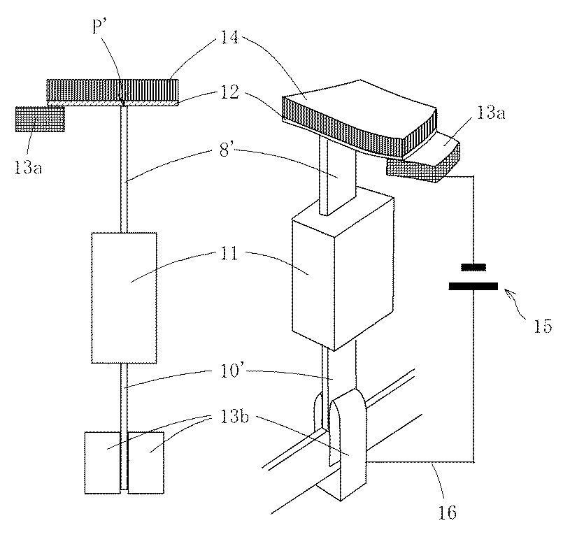
表1より明らかなように、実施例にかかる固体電解コンデンサは、従来例にかかる固体電解コンデンサと比較し、漏れ電流値および漏れ電流不良率が改善されている。 As is clear from Table 1, the solid electrolytic capacitor according to the example is improved in the leakage current value and the leakage current defect rate as compared with the solid electrolytic capacitor according to the conventional example.
これは、実施例にかかるエージング工程において、メタライズドフィルムとリード端子との接触面積が拡大することで、安定してエージングが行われたためと考えられる。 This is considered to be because the aging was stably performed by increasing the contact area between the metallized film and the lead terminal in the aging process according to the example.
なお、エージング前にリード端子に平面Pを形成する折り曲げ加工は、所定の製品形状にするために必要な折り曲げ加工であるため、余分な工程の追加は生じない。また、エージング装置も従来のものをそのまま使用することができる。 Note that the bending process for forming the flat surface P on the lead terminal before aging is a bending process necessary for obtaining a predetermined product shape, so that no additional process is added. A conventional aging apparatus can be used as it is.
また、上記実施例では陰極リード端子8に平面Pを形成してメタライズドフィルム12を当接させたが、陽極リード端子10に平面Pを形成してメタライズドフィルム12を当接させてもよい。
Further, in the above-described embodiment, the flat surface P is formed on the
また、エージング前におけるリード端子の折り曲げ工程を図2Bに示す段階で終了し、この段階で形成される平面Qに対してメタライズドフィルム12を当接させてもよい。
Further, the bending process of the lead terminal before aging may be finished at the stage shown in FIG. 2B, and the
P 平面
P’ 先端の面
Q 平面
1 陽極体
2 酸化皮膜層
3 固体電解質層
4 カーボン層
5 銀層
6 コンデンサ素子
7 導電性接着剤
8 陰極リード端子
9 陽極ワイヤ(タンタルワイヤ)
10 陽極リード端子
11 外装樹脂
12 メタライズドフィルム
13a、13b 給電端子
14 スポンジ
15 電源
16 給電用電線
17 フォーミングローラ
18 固体電解コンデンサ
19 導電性フレーム
20 絶縁用スペーサ
P plane P ′ tip
DESCRIPTION OF
Claims (1)
前記コンデンサ素子の陽極部および陰極部に対し、陽極リード端子および陰極リード端子を、互いに反対方向を向いて外方へ突出するようにそれぞれ接続する工程と、
前記コンデンサ素子ならびに前記陽極リード端子および陰極リード端子の基端側を外装樹脂で封止する工程と、
前記外装樹脂から突出している前記陽極リード端子および陰極リード端子の少なくとも一方を、突出方向に略垂直な平面を有する所定形状に折り曲げる工程と、
前記平面に対し、第1の給電端子に接続されたメタライズドフィルムを当接させると共に、他方のリード端子に対し第2の給電端子を接続し、当該第1および第2の給電端子間に所定電圧を印加して前記コンデンサ素子をエージングする工程と、
を有することを特徴とする固体電解コンデンサの製造方法。 Producing a capacitor element having an anode part on one side and a cathode part on the other side;
Connecting the anode lead terminal and the cathode lead terminal to the anode part and the cathode part of the capacitor element so as to protrude outward in opposite directions, respectively;
Sealing the capacitor element and the base end side of the anode lead terminal and the cathode lead terminal with an exterior resin;
Bending at least one of the anode lead terminal and the cathode lead terminal protruding from the exterior resin into a predetermined shape having a plane substantially perpendicular to the protruding direction;
A metallized film connected to the first power supply terminal is brought into contact with the plane, and a second power supply terminal is connected to the other lead terminal, and a predetermined voltage is applied between the first and second power supply terminals. Aging the capacitor element by applying
A method for producing a solid electrolytic capacitor, comprising:
Priority Applications (1)
| Application Number | Priority Date | Filing Date | Title |
|---|---|---|---|
| JP2006106244A JP2007281237A (en) | 2006-04-07 | 2006-04-07 | Method for manufacturing solid electrolytic capacitor |
Applications Claiming Priority (1)
| Application Number | Priority Date | Filing Date | Title |
|---|---|---|---|
| JP2006106244A JP2007281237A (en) | 2006-04-07 | 2006-04-07 | Method for manufacturing solid electrolytic capacitor |
Publications (1)
| Publication Number | Publication Date |
|---|---|
| JP2007281237A true JP2007281237A (en) | 2007-10-25 |
Family
ID=38682377
Family Applications (1)
| Application Number | Title | Priority Date | Filing Date |
|---|---|---|---|
| JP2006106244A Pending JP2007281237A (en) | 2006-04-07 | 2006-04-07 | Method for manufacturing solid electrolytic capacitor |
Country Status (1)
| Country | Link |
|---|---|
| JP (1) | JP2007281237A (en) |
Citations (3)
| Publication number | Priority date | Publication date | Assignee | Title |
|---|---|---|---|---|
| JPH05326342A (en) * | 1992-05-15 | 1993-12-10 | Nippon Chemicon Corp | Manufacture of solid electrolytic capacitor |
| JPH07272988A (en) * | 1994-03-30 | 1995-10-20 | Nichicon Corp | Metallized film used for aging of electronic parts |
| JP2004221224A (en) * | 2003-01-14 | 2004-08-05 | Sanyo Electric Co Ltd | Solid electrolytic capacitor |
-
2006
- 2006-04-07 JP JP2006106244A patent/JP2007281237A/en active Pending
Patent Citations (3)
| Publication number | Priority date | Publication date | Assignee | Title |
|---|---|---|---|---|
| JPH05326342A (en) * | 1992-05-15 | 1993-12-10 | Nippon Chemicon Corp | Manufacture of solid electrolytic capacitor |
| JPH07272988A (en) * | 1994-03-30 | 1995-10-20 | Nichicon Corp | Metallized film used for aging of electronic parts |
| JP2004221224A (en) * | 2003-01-14 | 2004-08-05 | Sanyo Electric Co Ltd | Solid electrolytic capacitor |
Similar Documents
| Publication | Publication Date | Title |
|---|---|---|
| JP5501935B2 (en) | Solid electrolytic capacitor element and manufacturing method thereof | |
| CN101996769B (en) | Solid electrolytic capacitor And Manufacturing approach | |
| CN107275091A (en) | Solid electrolytic capacitor | |
| JP5072857B2 (en) | Electrolytic capacitor manufacturing method | |
| US20090237865A1 (en) | Solid electrolytic capacitor and method for manufacturing same | |
| JP4662368B2 (en) | Manufacturing method of solid electrolytic capacitor | |
| JP2008141079A (en) | Electrolytic capacitor | |
| JP2005129622A (en) | Manufacturing method of solid electrolytic capacitor | |
| JP2011014663A (en) | Solid electrolytic capacitor | |
| JP2007281237A (en) | Method for manufacturing solid electrolytic capacitor | |
| JPWO2006114917A1 (en) | Multilayer solid electrolytic capacitor and manufacturing method thereof | |
| JP6475417B2 (en) | Solid electrolytic capacitor element, manufacturing method thereof, and solid electrolytic capacitor | |
| JP2007184308A (en) | Manufacturing method of chip-like solid electrolytic capacitor | |
| JP2009253020A (en) | Solid electrolytic capacitor | |
| JP4334423B2 (en) | Capacitor element manufacturing method | |
| JP2022039173A (en) | Electrolytic capacitor | |
| JP3367221B2 (en) | Electrolytic capacitor | |
| JP6305682B2 (en) | Aluminum electrolytic capacitor and manufacturing method thereof | |
| JP5273736B2 (en) | Manufacturing method of solid electrolytic capacitor | |
| JP2008305826A (en) | Solid electrolytic capacitor | |
| JP5898927B2 (en) | Chip type solid electrolytic capacitor | |
| JP4596939B2 (en) | Manufacturing method of three-terminal solid electrolytic capacitor element | |
| JP4761194B2 (en) | Chemical conversion method and chemical conversion apparatus | |
| JP2011049224A (en) | Solid electrolytic capacitor and method of manufacturing the same | |
| JP2007250920A (en) | Method for manufacturing solid electrolytic capacitor |
Legal Events
| Date | Code | Title | Description |
|---|---|---|---|
| A621 | Written request for application examination |
Free format text: JAPANESE INTERMEDIATE CODE: A621 Effective date: 20081023 |
|
| A131 | Notification of reasons for refusal |
Free format text: JAPANESE INTERMEDIATE CODE: A131 Effective date: 20110302 |
|
| A02 | Decision of refusal |
Free format text: JAPANESE INTERMEDIATE CODE: A02 Effective date: 20110706 |