JP2007227672A - Imaging apparatus - Google Patents
Imaging apparatus Download PDFInfo
- Publication number
- JP2007227672A JP2007227672A JP2006047366A JP2006047366A JP2007227672A JP 2007227672 A JP2007227672 A JP 2007227672A JP 2006047366 A JP2006047366 A JP 2006047366A JP 2006047366 A JP2006047366 A JP 2006047366A JP 2007227672 A JP2007227672 A JP 2007227672A
- Authority
- JP
- Japan
- Prior art keywords
- opening
- pixel region
- electrode
- image sensor
- imaging device
- Prior art date
- Legal status (The legal status is an assumption and is not a legal conclusion. Google has not performed a legal analysis and makes no representation as to the accuracy of the status listed.)
- Pending
Links
Images


Abstract
Description
この発明は、撮像装置、詳しくは電気基板に対してベアチップからなる撮像素子及び保護ガラスとを接着固定して形成される撮像装置に関するものである。 The present invention relates to an image pickup apparatus, and more particularly to an image pickup apparatus formed by bonding and fixing an image pickup element made of a bare chip and a protective glass to an electric substrate.
従来より、撮影光学系に入射する被写体からの光束に基づいて形成される被写体像を、所定の位置に配置したベアチップからなる撮像素子(例えば電荷結合素子(CCD;Charge Coupled Device)等)の受光面上に結像させ、この被写体像を所定の形態の画像データ等として記録し得るように構成したデジタルカメラ等の電子機器が一般的に実用化され広く普及している。 Conventionally, a subject image formed on the basis of a light beam from a subject incident on a photographing optical system is received by an image pickup device (for example, a charge coupled device (CCD) or the like) including a bare chip arranged at a predetermined position. 2. Description of the Related Art Electronic devices such as digital cameras configured to form an image on a surface and record the subject image as image data of a predetermined form are generally put into practical use and widely used.
デジタルカメラ等に組み込まれる撮像装置として、例えば特開2002−218293号公報等によって開示されているようなベアチップ実装構造がある(同公報図2参照)。 As an imaging device incorporated in a digital camera or the like, there is a bare chip mounting structure as disclosed in, for example, Japanese Patent Application Laid-Open No. 2002-218293 (see FIG. 2).
即ち、保護ガラスに対してフレキシブルプリント基板(FPC)が接着剤を用いて接着されている。このフレキシブルプリント基板において保護ガラスが接着されている接着面とは反対側の面に対してベアチップからなる撮像素子が電極パッド,バンプを介して接続されている。この場合において、撮像素子の受光面は、保護ガラスに対向するように配置されている。 That is, a flexible printed circuit board (FPC) is bonded to the protective glass using an adhesive. In this flexible printed circuit board, an image pickup element made of a bare chip is connected to the surface opposite to the bonding surface to which the protective glass is bonded via electrode pads and bumps. In this case, the light receiving surface of the image sensor is disposed so as to face the protective glass.
そして、この電極パッド,バンプには、これを覆うように接着剤が塗布される。これにより、フレキシブルプリント基板と撮像素子とが接着結合されると共に、撮像素子の受光面(画素領域)の封止構造が形成されている。 An adhesive is applied to the electrode pads and bumps so as to cover them. As a result, the flexible printed circuit board and the image sensor are adhesively bonded, and a sealing structure for the light receiving surface (pixel region) of the image sensor is formed.
上述したように、従来の一般的な撮像装置においては、柔軟な板状部材であるフレキシブルプリント基板に対して硬質な板状部材からなるベアチップ(撮像素子)を接着剤により接着するようなベアチップ実装構造からなるものがある。 As described above, in a conventional general imaging apparatus, bare chip mounting in which a bare chip (imaging device) made of a hard plate member is bonded to a flexible printed board, which is a flexible plate member, with an adhesive. Some are made up of structures.
通常のベアチップからなる撮像素子においては、チップ形状に対して画素領域が極力大きくなるように設計されるのが普通である。したがって、ベアチップ(撮像素子)の画素領域が形成される面と同一面にあって、この画素領域に隣接する部位に設けられる電極と、当該画素領域の周縁部との間が短い間隔になってしまう傾向がある。
ところが、従来の撮像装置における上述したようなベアチップ実装構造からなるものでは、接着部における充分な接着強度を確保することができないことがある。 However, in the conventional imaging device having the bare chip mounting structure as described above, it may not be possible to secure sufficient adhesive strength at the bonding portion.
例えば、図10に示すように、ベアチップからなる撮像素子121とフレキシブルプリント基板117とを接着剤131を用いて接続するベアチップ実装構造からなる撮像装置において、画素領域121aの周縁部と電極130の内側端部との間隔が短く設定されている場合には、当該撮像素子121とフレキシブルプリント基板117との間の接着剤131による接着範囲Cのうち電極130よりも内側の部分、即ち電極130と画素領域121aとの間の部分での接着範囲B’を充分に確保できないことになる。したがって、この場合には、充分な接着信頼性を確保することができないという問題点がある。
For example, as shown in FIG. 10, in an imaging device having a bare chip mounting structure in which an
本発明は、上述した点に鑑みてなされたものであって、その目的とするところは、電気基板に対してベアチップ(撮像素子)を実装するベアチップ実装構造を有する撮像装置において、電気基板とベアチップ(撮像素子)との接着部位の接着強度を充分に確保して信頼性を備えた撮像装置を提供することである。 The present invention has been made in view of the above points, and an object of the present invention is to provide an electric substrate and a bare chip in an imaging device having a bare chip mounting structure for mounting a bare chip (imaging element) on an electric substrate. It is to provide an imaging apparatus having sufficient reliability by sufficiently securing the bonding strength of the bonding part with the (imaging element).
上記目的を達成するために、本発明による撮像装置は、撮像装置において、画素領域と、この画素領域と同一面にあって、この画素領域に隣接する部位に設けられた電極とを有するベアチップからなる撮像素子と、開口と、この開口を覆うように上記撮像素子が配置され、この開口の縁部近傍に配置され上記電極と接続するための接続パターンとを有し、上記電極から上記画素領域に向けて0.3mm以上離れた位置に上記開口の開口内縁が形成される電気基板とを有することを特徴とする。 In order to achieve the above object, an imaging apparatus according to the present invention is an imaging apparatus comprising a bare chip having a pixel region and an electrode provided in a portion adjacent to the pixel region and in the same plane as the pixel region. An image sensor, an opening, the image sensor is disposed so as to cover the aperture, and a connection pattern disposed near the edge of the aperture to connect to the electrode. And an electric substrate on which the inner edge of the opening is formed at a position separated by 0.3 mm or more.
本発明によれば、電気基板に対してベアチップ(撮像素子)を実装するベアチップ実装構造を有する撮像装置において、電気基板とベアチップ(撮像素子)との接着部位の接着強度を充分に確保して信頼性を備えた撮像装置を提供することができる。 According to the present invention, in an imaging apparatus having a bare chip mounting structure for mounting a bare chip (imaging element) on an electric substrate, sufficient adhesion strength at a bonding portion between the electric substrate and the bare chip (imaging element) is ensured and reliable. It is possible to provide an imaging device having the characteristics.
以下、図示の実施の形態によって本発明を説明する。 The present invention will be described below with reference to the illustrated embodiments.
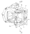
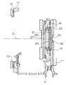
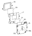
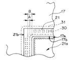
図1,図2は、本発明の一実施形態の撮像装置が適用されるデジタル一眼レフレックスカメラ(以下、単にデジタルカメラという)のミラーボックス部分を取り出して示す図である。このうち、図1はボディマウント及びその他説明に不要な機構部を除いた当該ミラーボックス部分の斜視図である。図2は、図1の[II]−[II]線に沿う断面図である。また、図3は、本実施形態の撮像装置の構成を示す正面図である。図4,図6は、本実施形態の撮像装置の構成を示す分解斜視図である。このうち、図4は、前側からみた図である。図6は、背面側から見た図である。図5,図7は、本実施形態の撮像装置を組み立てた状態の斜視図である。このうち、図5は、前側からみた図である。図7は、背面側から見た図である。図8は、本実施形態の撮像装置において、フレキシブルプリント基板に対して撮像素子が接着固定された状態を示す要部拡大断面図である。図9は、図8に示す矢印X方向から見た際の要部拡大平面図である。 1 and 2 are views showing a mirror box portion of a digital single-lens reflex camera (hereinafter simply referred to as a digital camera) to which an imaging apparatus according to an embodiment of the present invention is applied. Among these, FIG. 1 is a perspective view of the mirror box portion excluding the body mount and other unnecessary mechanism portions. 2 is a cross-sectional view taken along line [II]-[II] in FIG. FIG. 3 is a front view showing the configuration of the imaging apparatus of the present embodiment. 4 and 6 are exploded perspective views showing the configuration of the imaging apparatus of the present embodiment. Among these, FIG. 4 is a view seen from the front side. FIG. 6 is a view as seen from the back side. 5 and 7 are perspective views in a state in which the imaging device according to the present embodiment is assembled. Among these, FIG. 5 is a view seen from the front side. FIG. 7 is a view from the back side. FIG. 8 is an essential part enlarged cross-sectional view showing a state in which the imaging element is bonded and fixed to the flexible printed board in the imaging apparatus of the present embodiment. FIG. 9 is an enlarged plan view of a main part when viewed from the direction of the arrow X shown in FIG.
図1に示すように、ミラーボックス10の本体部11の前面には、ボディマウント13(図1では図示せず。図2参照)が載置されるマウント載置面13aがある。このボディマウント13は、撮影光学系を有する撮影レンズ鏡筒(図示せず)を本体部11に対して着脱自在とするために設けられているものである。したがって、当該ボディマウント13にレンズ鏡筒(図示せず)を装着したとき、レンズ鏡筒の撮影光学系の光軸O(図2参照)は、ボディマウント13の略中心部を通過するように、かつボディマウント13のマウント面は、撮影光学系の光軸Oに対して略直交する面となるように設定されている。
As shown in FIG. 1, a
本体部11の後方には、後述する撮像素子21等を含み固定部材15,保護部材16,フレキシブルプリント基板17(FPC)等によって構成される本実施形態の撮像装置が、当該本体部11に対して固設されている。
Behind the
本実施形態の撮像装置は、図2〜図5に示すように固定部材15,保護部材16,フレキシブルプリント基板17,放熱部材20,撮像素子21,保護ガラス24等によって主に構成されている。
The imaging apparatus of the present embodiment is mainly configured by a
固定部材15は、ミラーボックス10に対する当該撮像装置の位置決めの基準となる部材である。なお、固定部材15は、板状の硬質部材、例えば金属部材であるアルミ材,ステンレス材等や、セラミック,モールド部品等によって形成される。
The
保護部材16は、フレキシブルプリント基板17に固着されている。そして、保護部材16は、撮像素子21や保護ガラス24とフレキシブルプリント基板17との接着部に対してフレキシブルプリント基板17が屈曲することにより生じる応力から保護する機能や、当該撮像装置を組み立てる際に固定部材15に対するフレキシブルプリント基板17の位置決めをするために用いられるものである。
The
撮像素子21は、撮影光学系(図示せず)を透過して結像される光学的な被写体像に応じた画像信号を生成する光電変換処理を行なう光電変換素子である。この撮像素子21は、例えば電荷結合素子(CCD;Charge Coupled Device)等のベアチップにより形成されている。撮像素子21の一方の面(受光面)には、画素領域21a(図8参照)が形成されている。この画素領域21aの形成されている面と同一面にあって、画素領域21aに隣接する部位、即ち撮像素子21の周囲である外周縁部近傍には、複数個の電極30が設けられている。この電極30は、フレキシブルプリント基板17の接続パターン(図示せず)にバンプで接続されることで、フレキシブルプリント基板17と撮像素子21との間の信号の授受が行なわれるようになっている。
The
フレキシブルプリント基板17は、撮像素子21により光電変換処理がなされて生成された画像信号を画像処理回路等の電気回路(図示せず)に対して供給するために設けられる電気基板である。フレキシブルプリント基板17の略中央部分には、略矩形状の開口17a(図4参照)が形成されている。この開口17aは、撮像する光束を通過させるために設けられるものである。したがって、当該開口17aは、撮像素子21の画素領域21aよりも大きく、そして撮像素子21の外形より小さく、かつ電極30のある位置よりも内側に設定されている。この開口17aの縁部近傍には、撮像素子21の電極30と接続する接続パターン(図示せず)が形成されている。
The flexible printed
放熱部材20は、撮像素子21に蓄積された熱を放出するために設けられているものである。この放熱部材20は、例えばセラミック等の板状部材によって形成されている。
The
保護ガラス24は、撮像素子21より外形が大きく、撮像素子21の受光面(撮像領域)に対向する部位に設けられることによって、撮像素子21の撮像領域を保護するために設けられる保護カバーである。この保護ガラス24は、例えば平板形状のガラス等の透明部材等によって形成されている。
The
保護ガラス24は、フレキシブルプリント基板17の撮像素子21が固着されている面とは反対側の面に開口17aを覆うように接着剤25によって固着されている。
The
なお、図2に示すように、保護ガラス24の前面側には、撮影光学系(図示せず)を透過して入射してくる被写体からの光束(以下、輔車体光束という)から高周波成分を取り除く光学ローパスフイルター(Low Pass Filter;以下、光学LPFと略記する)26と、撮像素子21の受光面に向けて入射される被写体光束の照射時間等を制御するシャッター27とが順次配設されている。
As shown in FIG. 2, a high frequency component is generated on the front side of the
本実施形態の撮像装置における各構成部材の部材配置は、次に示す通りである。 The member arrangement of each constituent member in the imaging apparatus of the present embodiment is as follows.
フレキシブルプリント基板17の一方の面、即ち裏面側には、開口17aを覆うように撮像素子21が配置される。この場合において、フレキシブルプリント基板17と撮像素子21とは、接着剤31によって少なくとも機械的に固着される。
On one surface of the flexible printed
つまり、フレキシブルプリント基板17の裏面側であって開口17aの周縁部と、撮像素子21の一方の面、即ち受光面(画素領域21a)と同一面側の外周縁部とは、電極30(図8参照)のバンプ部分を除いて接着剤31により接着固定される。
That is, the periphery of the
より詳しく言えば、接着剤31は、撮像素子21の外縁21bから少なくともフレキシブルプリント基板17の接続パターンと撮像素子21の電極30との電気的接続部分まで撮像素子21とフレキシブルプリント基板17の間と、かつ撮像素子21の周縁に沿って第一の帯幅で環状に塗布される。つまり、接着剤31は、フレキシブルプリント基板17の開口17aの周囲に塗布される。
More specifically, the adhesive 31 is between the
そして、接着剤31は、撮像素子21の外縁21bからフレキシブルプリント基板17の接続パターンと電極30との電気的接続部分を包むように、撮像素子21の周縁に沿って帯状に塗布される。これにより、撮像素子21は、フレキシブルプリント基板17の裏面側の所定の部位に対して固着した状態で、撮像素子21の画素領域21aが開口17aから露呈するように配置される。
The adhesive 31 is applied in a strip shape along the periphery of the
フレキシブルプリント基板17の他方の面、即ち表面側であって開口17aの周縁部と、保護ガラス24の裏面側の外周縁部とは、接着剤25によって接着されている。
The other surface of the flexible printed
より詳しく言うと、接着剤25は、フレキシブルプリント基板17の開口17aの周囲に第二の帯幅で環状に塗布される。なお、この部分に用いられる接着剤25は、例えば紫外線硬化型のもの等が適用される。
More specifically, the adhesive 25 is annularly applied around the
この保護ガラス24とフレキシブルプリント基板17とを接着することによって、撮像素子21の受光面近傍をの空間を外部に対して封止して、当該受光面を外部から保護する封止構造が形成されている。
By bonding the
一方、撮像素子21の裏面側、即ち撮像素子21の受光面とは反対側の面には、放熱部材20が接着剤(図2参照)により接着されている。
On the other hand, the
さらに、この放熱部材20の背面側には、固定部材15が、固定部材15に穿設されている孔15aを介して接着剤32により接着固定されている。また、孔15bは、放熱部材20を固定部材15に対して接着する際に用いられる。なお、固定部材15に対する放熱部材20の接着手段についての詳細は、本発明に関連しない点であるので、その説明は省略する。
Further, the fixing
そして、この固定部材15は、本体部11の所定の部位に対してビス止め等の手段により固定されている。したがって、これにより撮像素子21はミラーボックス10の本体部11の所定の部位に対して固設されている。
The fixing
次に、フレキシブルプリント基板17と撮像素子21の接着部位について、以下に詳述する。
Next, the adhesion site | part of the flexible printed
上述したように、撮像素子21の受光面側の外周縁部とフレキシブルプリント基板17の裏面側であって開口17aの周縁部とは、電極30の周囲に周り込んだ接着剤31により接着固定される。この接着剤31は、特に絶縁性のものが用いられる。そして、接着剤31は、撮像素子21の外縁21bからフレキシブルプリント基板17の接続パターンと電極30との電気的接続部分の周囲を包むように、撮像素子21の周縁に沿って帯状に分布することで、電極30近傍の絶縁性が確保されている。
As described above, the outer peripheral edge portion on the light receiving surface side of the
ここで、撮像素子21とフレキシブルプリント基板17との接着剤31による接着範囲(塗布範囲)のうち、電極30の端部から内側、即ち画素領域21aの周縁部に向けた方向の接着範囲を符号Aで表わすものとする(図8,図9参照)。
Here, in the adhesion range (application range) of the
また、電極30の端部から内側に向けてフレキシブルプリント基板17の開口17aの内縁端部17bまでの間隔を符号Bで表わすものとする(図8,図9参照)。
In addition, the distance from the end of the
本実施形態の撮像装置では、図8,図9に示すように、フレキシブルプリント基板17の開口17aの内縁端部17bは、電極30の内側端部から画素領域21aの周縁部に向けて0.3mm以上離れた位置(B≧0.3mm)となるように設定されている。
In the imaging apparatus of the present embodiment, as shown in FIGS. 8 and 9, the
そして、接着剤31による接着範囲のうち電極30の端部から画素領域21aの周縁部に向けた方向の接着範囲Aは、電極30からフレキシブルプリント基板17の開口17aの内縁端部17bまでの間、即ち上記間隔寸法Bの範囲内に収まるように設定されている。つまり、接着範囲Aは、電極30の内側端部から0.3mmよりも小となるように設定される(B≧0.3mm>A)。
The adhesion range A in the direction from the end of the
また、フレキシブルプリント基板17の開口17aの寸法公差を考慮した場合には、その寸法ばらつき分だけ開口17aが小さいものとして考える必要がある。例えば、開口17aの寸法公差を±0.05mmとした場合には、上記間隔寸法Bは、
B≧0.3mm+0.05mm×2
≧0.4mm
に設定されることがより好ましい。言い換えれば、画素領域21aの外周から電極30の端部までの距離が0.4mm以上であるということができる。
Further, when considering the dimensional tolerance of the
B ≧ 0.3mm + 0.05mm × 2
≧ 0.4mm
More preferably, it is set to. In other words, it can be said that the distance from the outer periphery of the pixel region 21a to the end of the
なお、画素領域21aに対して入射する光線D(図9参照)の入射角度を考慮すると、画素領域21aの周縁部と開口17aの内縁端部17bとが重ならないように、かつ画素領域21aの外周サイズよりも開口17aのサイズの方が大きくなるように、上記間隔寸法Bを設定する必要がある。
In consideration of the incident angle of the light ray D (see FIG. 9) incident on the pixel region 21a, the peripheral portion of the pixel region 21a and the
以上説明したように上記一実施形態によれば、電極30の端部から画素領域21aに向けて0.3mm以上離れた位置または0.4mm以上離れた位置にフレキシブルプリント基板17の開口17aの内縁端部17bを形成するように設定したので、フレキシブルプリント基板17と撮像素子21との間の接着剤31の接着範囲を充分にとることができ、よって充分な接着強度を確保して、信頼性を備えた撮像装置とすることができる。
As described above, according to the above-described embodiment, the inner edge of the
なお、上記一実施形態においては、保護ガラス24の適用例として、平板形状のガラス等の透明部材等としているが、これに限ることはない。保護ガラス24の例としては、ほかに例えばローパスフイルターでもよいし、赤外線カットフイルター等としても、同様に適用することができる。
In the above-described embodiment, as an application example of the
また、上述の一実施形態では、電気基板の例としてフレキシブルプリント基板17を用いて説明しているが、これに限ることはない。電気基板の適用例としては、例えば硬質の薄型基板等を適用しても同様である。
In the above-described embodiment, the flexible printed
また、上述の位置実施形態においては、絶縁性を有する接着剤31を用いて撮像素子21と電気基板であるフレキシブルプリント基板17とを接着するようにしているが、これに限ることはない。例えば、撮像素子21とフレキシブルプリント基板17とは、押圧により導電性を有する導電粒子を含む接着剤を用いてもよいことはもちろんである。
Further, in the above-described position embodiment, the
10……ミラーボックス
11……本体部
13……ボディマウント
13a……マウント載置面
15……アルミ板
15a,15b……孔
16……保護部材
17……フレキシブルプリント基板
17a……開口
17b……内縁端部
20……放熱部材
21,121……撮像素子
21a,121a……画素領域
24……保護ガラス
25,31,32,131……接着剤
30,130……電極
DESCRIPTION OF SYMBOLS 10 ...
Claims (6)
画素領域と、この画素領域と同一面にあって、この画素領域に隣接する部位に設けられた電極とを有するベアチップからなる撮像素子と、
開口と、この開口を覆うように上記撮像素子が配置され、この開口の縁部近傍に配置され上記電極と接続するための接続パターンとを有し、上記電極から上記画素領域に向けて0.3mm以上離れた位置に上記開口の開口内縁が形成される電気基板と、
を有することを特徴とする撮像装置。 In the imaging device,
An image sensor made up of a bare chip having a pixel region and an electrode that is on the same plane as the pixel region and is adjacent to the pixel region;
The imaging element is disposed so as to cover the opening, and has a connection pattern disposed in the vicinity of the edge of the opening and connected to the electrode. An electric substrate on which an inner edge of the opening is formed at a position separated by 3 mm or more;
An imaging device comprising:
画素領域と、この画素領域と同一面にあって、この画素領域に隣接する部位に設けられた電極とを有するベアチップからなる撮像素子と、
開口と、この開口を覆うように上記撮像素子が配置され、この開口の縁部近傍に配置され上記電極と接続するための接続パターンとを有し、上記電極から上記画素領域に向けて0.4mm以上離れた位置に上記開口の開口内縁が形成される電気基板と、
を有することを特徴とする撮像装置。 In the imaging device,
An image sensor made up of a bare chip having a pixel region and an electrode that is on the same plane as the pixel region and is adjacent to the pixel region;
The imaging element is disposed so as to cover the opening, and has a connection pattern disposed in the vicinity of the edge of the opening and connected to the electrode. An electric substrate on which an opening inner edge of the opening is formed at a position separated by 4 mm or more;
An imaging device comprising:
画素領域と、この画素領域と同一面にあって、この画素領域に隣接する部位に設けられた電極とを有するベアチップからなる撮像素子と、
開口と、この開口を覆うように上記撮像素子が配置され、この開口の縁部近傍に配置され上記電極と接続するための接続パターンとを有する電気基板であって、この電気基板と上記撮像素子とを固着させるため、接着剤が上記撮像素子の外縁から少なくとも上記接続パターンと上記電極との電気的接続部分を包むように上記撮像素子の周縁に沿って帯状に塗布され、上記電極の端部から上記画素領域に向けて0.3mm以上離れた位置に上記開口の開口内縁が形成される電気基板と、
を有することを特徴とする撮像装置。 In the imaging device,
An image sensor made up of a bare chip having a pixel region and an electrode that is on the same plane as the pixel region and is adjacent to the pixel region;
An electric board having an opening and the imaging element disposed so as to cover the opening, and a connection pattern arranged in the vicinity of the edge of the opening and connected to the electrode, the electric board and the imaging element Adhesive is applied in a belt shape along the periphery of the image sensor so as to wrap at least the electrical connection portion between the connection pattern and the electrode from the outer edge of the image sensor, and from the end of the electrode An electric substrate in which an opening inner edge of the opening is formed at a position separated by 0.3 mm or more toward the pixel region;
An imaging device comprising:
画素領域と、この画素領域と同一面にあって、この画素領域に隣接する部位に設けられた電極とを有するベアチップからなる撮像素子と、
開口と、この開口を覆うように上記撮像素子が配置され、この開口の縁部近傍に配置され上記電極と接続するための接続パターンとを有する電気基板であって、この電気基板と上記撮像素子とを固着させるため、接着剤が上記撮像素子の外縁から少なくとも上記接続パターンと上記電極との電気的接続部分を包むように上記撮像素子の周縁に沿って帯状に塗布され、上記電極の端部から上記画素領域に向けて0.4mm以上離れた位置に上記開口の開口内縁が形成される電気基板と、
を有することを特徴とする撮像装置。 In the imaging device,
An image sensor made up of a bare chip having a pixel region and an electrode that is on the same plane as the pixel region and is adjacent to the pixel region;
An electric board having an opening and the imaging element disposed so as to cover the opening, and a connection pattern arranged in the vicinity of the edge of the opening and connected to the electrode, the electric board and the imaging element Adhesive is applied in a belt shape along the periphery of the image sensor so as to wrap at least the electrical connection portion between the connection pattern and the electrode from the outer edge of the image sensor, and from the end of the electrode An electric substrate in which an opening inner edge of the opening is formed at a position separated by 0.4 mm or more toward the pixel region;
An imaging device comprising:
開口と該開口の周囲に複数の接続パターンとを有する電気基板と、
画素領域と、上記接続用パターンと電気的に接続されるため該画素領域と同一面に該画素領域の外周に沿って該画素領域から0.4mmの間隔を離して設けられた電極とを有し、上記電気基板の上記開口を覆うように上記電気基板に実装されるベアチップからなる撮像素子と、
を有することを特徴とする撮像装置。 In the imaging device,
An electric board having an opening and a plurality of connection patterns around the opening;
In order to be electrically connected to the connection pattern, the pixel area has electrodes disposed on the same plane as the pixel area along the outer periphery of the pixel area and spaced apart from the pixel area by 0.4 mm. And an image sensor composed of a bare chip mounted on the electric substrate so as to cover the opening of the electric substrate,
An imaging device comprising:
Priority Applications (3)
| Application Number | Priority Date | Filing Date | Title |
|---|---|---|---|
| JP2006047366A JP2007227672A (en) | 2006-02-23 | 2006-02-23 | Imaging apparatus |
| CN2007100070875A CN101026690B (en) | 2006-02-23 | 2007-02-08 | Image pickup apparatus |
| US11/709,116 US7750279B2 (en) | 2006-02-23 | 2007-02-20 | Image pickup apparatus and image pickup unit |
Applications Claiming Priority (1)
| Application Number | Priority Date | Filing Date | Title |
|---|---|---|---|
| JP2006047366A JP2007227672A (en) | 2006-02-23 | 2006-02-23 | Imaging apparatus |
Publications (1)
| Publication Number | Publication Date |
|---|---|
| JP2007227672A true JP2007227672A (en) | 2007-09-06 |
Family
ID=38549176
Family Applications (1)
| Application Number | Title | Priority Date | Filing Date |
|---|---|---|---|
| JP2006047366A Pending JP2007227672A (en) | 2006-02-23 | 2006-02-23 | Imaging apparatus |
Country Status (2)
| Country | Link |
|---|---|
| JP (1) | JP2007227672A (en) |
| CN (1) | CN101026690B (en) |
Cited By (2)
| Publication number | Priority date | Publication date | Assignee | Title |
|---|---|---|---|---|
| JP2011512559A (en) * | 2008-02-15 | 2011-04-21 | 株式会社オプトエレクトロニクス | Printed circuit and optical assembly |
| JP2013138223A (en) * | 2013-02-05 | 2013-07-11 | Optoelectronics Co Ltd | Method for connection between lens and flexible printed circuit and optical assembly |
Families Citing this family (2)
| Publication number | Priority date | Publication date | Assignee | Title |
|---|---|---|---|---|
| JP2012238687A (en) * | 2011-05-11 | 2012-12-06 | Sony Corp | Semiconductor package, semiconductor device manufacturing method and solid state image pickup device |
| CN107547778B (en) * | 2016-06-23 | 2020-12-18 | 宁波舜宇光电信息有限公司 | Photosensitive assembly and camera module |
Family Cites Families (2)
| Publication number | Priority date | Publication date | Assignee | Title |
|---|---|---|---|---|
| JP3607160B2 (en) * | 2000-04-07 | 2005-01-05 | 三菱電機株式会社 | Imaging device |
| TWI264224B (en) * | 2004-07-28 | 2006-10-11 | Fujitsu Ltd | Imaging apparatus |
-
2006
- 2006-02-23 JP JP2006047366A patent/JP2007227672A/en active Pending
-
2007
- 2007-02-08 CN CN2007100070875A patent/CN101026690B/en not_active Expired - Fee Related
Cited By (2)
| Publication number | Priority date | Publication date | Assignee | Title |
|---|---|---|---|---|
| JP2011512559A (en) * | 2008-02-15 | 2011-04-21 | 株式会社オプトエレクトロニクス | Printed circuit and optical assembly |
| JP2013138223A (en) * | 2013-02-05 | 2013-07-11 | Optoelectronics Co Ltd | Method for connection between lens and flexible printed circuit and optical assembly |
Also Published As
| Publication number | Publication date |
|---|---|
| CN101026690A (en) | 2007-08-29 |
| CN101026690B (en) | 2012-01-18 |
Similar Documents
| Publication | Publication Date | Title |
|---|---|---|
| JP6597729B2 (en) | Imaging unit and imaging apparatus | |
| JP4555732B2 (en) | Imaging device | |
| JP4668036B2 (en) | Mounting structure for FPC of image sensor | |
| JP5730678B2 (en) | IMAGING DEVICE AND ELECTRONIC DEVICE USING THE SAME | |
| JP4818750B2 (en) | Imaging device | |
| JP6232789B2 (en) | Imaging unit and imaging apparatus | |
| JP2007227672A (en) | Imaging apparatus | |
| JP6639290B2 (en) | Imaging device | |
| US7750279B2 (en) | Image pickup apparatus and image pickup unit | |
| JP6631610B2 (en) | Imaging unit and imaging device | |
| JP2013042359A (en) | Imaging apparatus | |
| JP2008103957A (en) | Imaging unit and image apparatus | |
| JP2007194272A (en) | Imaging module | |
| JP2015015529A (en) | Imaging unit and imaging apparatus | |
| JP2007227674A (en) | Photographing apparatus | |
| JP6756357B2 (en) | Imaging device | |
| JP2014179448A (en) | Imaging unit and imaging apparatus | |
| JP6443494B2 (en) | Imaging unit and imaging apparatus | |
| JP2007194271A (en) | Structure of mounting imaging element | |
| JP6675241B2 (en) | Imaging device | |
| JP2006081008A (en) | Optical device | |
| JP6145988B2 (en) | The camera module | |
| JP6111866B2 (en) | Imaging unit and imaging apparatus | |
| JP2018189667A (en) | Imaging apparatus | |
| JP2010205770A (en) | Imaging device |