JP2007199708A - Display device and manufacturing method thereof - Google Patents
Display device and manufacturing method thereof Download PDFInfo
- Publication number
- JP2007199708A JP2007199708A JP2006351955A JP2006351955A JP2007199708A JP 2007199708 A JP2007199708 A JP 2007199708A JP 2006351955 A JP2006351955 A JP 2006351955A JP 2006351955 A JP2006351955 A JP 2006351955A JP 2007199708 A JP2007199708 A JP 2007199708A
- Authority
- JP
- Japan
- Prior art keywords
- electrode
- film
- conductive film
- transistor
- reflective
- Prior art date
- Legal status (The legal status is an assumption and is not a legal conclusion. Google has not performed a legal analysis and makes no representation as to the accuracy of the status listed.)
- Withdrawn
Links
Images


Landscapes
- Liquid Crystal (AREA)
- Devices For Indicating Variable Information By Combining Individual Elements (AREA)
Abstract
Description
本発明は、画素電極を有する半導体装置、特に表示装置に関する。特に、1つの画素に、反射領域と透過領域とを有する半透過型の液晶表示装置に関する。 The present invention relates to a semiconductor device having a pixel electrode, and more particularly to a display device. In particular, the present invention relates to a transflective liquid crystal display device having a reflective region and a transmissive region in one pixel.
表示装置には、自発光の表示装置と非発光の表示装置とがあり、液晶表示装置は、非発光の表示装置の最も代表的なものである。非発光であるため、通常は、バックライトからの光を液晶表示装置に照射して、表示を行っている。 The display device includes a self-light emitting display device and a non-light emitting display device, and the liquid crystal display device is the most typical non-light emitting display device. Since it does not emit light, display is usually performed by irradiating the liquid crystal display device with light from the backlight.
しかしながら、バックライトからの光を利用した透過型の液晶表示装置は、通常の室内では表示画像を見易いが、太陽光の下では表示画像を見辛いという問題がある。特に、カメラ及び携帯情報端末、携帯電話機等の屋外で頻繁に活用される電子機器においては、この問題による影響は大きい。 However, the transmissive liquid crystal display device using light from the backlight has a problem that it is easy to see a display image in a normal room, but it is difficult to see the display image under sunlight. In particular, in electronic devices that are frequently used outdoors, such as cameras, personal digital assistants, and mobile phones, the effect of this problem is significant.
そこで、室内でも屋外でも良好な画像を表示できるようにするため、半透過型の液晶表示装置が開発されている。半透過型の液晶表示装置は、1つの画素の中に、反射領域と透過領域とを有している。透過領域には、透明電極を有し、そこで光を透過させて、透過型液晶表示装置として機能する。一方、反射領域には、反射電極を有し、そこで光を反射させて、反射型液晶表示装置として機能する。このようにすることにより、室内でも屋外でも良好な画像を表示することができる。 Therefore, a transflective liquid crystal display device has been developed in order to display a good image both indoors and outdoors. A transflective liquid crystal display device has a reflective region and a transmissive region in one pixel. The transmissive region has a transparent electrode and transmits light therethrough to function as a transmissive liquid crystal display device. On the other hand, the reflective region has a reflective electrode, which reflects light and functions as a reflective liquid crystal display device. In this way, a good image can be displayed both indoors and outdoors.
このような液晶表示装置としては、パッシブマトリクス型とアクティブマトリクス型とがある。アクティブマトリクス型の表示装置を作製する際は、一般的に、薄膜トランジスタ(TFT:Thin Film Transistor)の半導体層に接続する配線を形成し、その配線の上に画素電極となる導電膜を形成する。 Such liquid crystal display devices include a passive matrix type and an active matrix type. When an active matrix display device is manufactured, a wiring connected to a semiconductor layer of a thin film transistor (TFT) is generally formed, and a conductive film to be a pixel electrode is formed over the wiring.
画素電極としては、反射領域における反射電極と透過領域における透明電極とがある。各々は、形状が異なる。したがって、反射電極を形成するためのレジストマスクと、透明電極を形成するためのレジストマスクが必要だった(例えば特許文献1〜特許文献5参照)。
従来の半透過型液晶表示装置において、反射電極と透明電極を形成する際はレジストマスクがそれぞれの層において必要であった。つまり、反射電極を形成するレジストマスクと、透明電極と積層する膜のエッチング用のレジストマスクとが必要であり、その分だけ作製工程数が多かった。そのため、表示装置のような半導体装置の製造コストが高く、電極パターンを形成するための製造時間も長く必要であった。 In a conventional transflective liquid crystal display device, a resist mask is required for each layer when forming a reflective electrode and a transparent electrode. That is, a resist mask for forming a reflective electrode and a resist mask for etching a film to be laminated with a transparent electrode are necessary, and the number of manufacturing steps is increased accordingly. Therefore, the manufacturing cost of a semiconductor device such as a display device is high, and a manufacturing time for forming an electrode pattern is also required to be long.
そこで、本発明は、使用するレジストマスクの数を減らし、作製工程を短縮することを課題とする。 Therefore, an object of the present invention is to reduce the number of resist masks to be used and shorten the manufacturing process.
本発明は、トランジスタと、該トランジスタに電気的に接続する透明電極と、該透明電極に電気的に接続する反射電極と、該トランジスタに電気的に接続する保持容量と、を有し、該反射電極の下に、該保持容量の少なくとも一部が形成され、該反射電極の下面全体が該透明電極の上面に接していることを特徴とする表示装置が提供される。 The present invention includes a transistor, a transparent electrode that is electrically connected to the transistor, a reflective electrode that is electrically connected to the transparent electrode, and a storage capacitor that is electrically connected to the transistor. A display device is provided in which at least a part of the storage capacitor is formed under the electrode, and the entire lower surface of the reflective electrode is in contact with the upper surface of the transparent electrode.
また、本発明は、トランジスタと、該トランジスタに電気的に接続する透明電極と、該透明電極に電気的に接続する反射電極と、を有し、該透明電極もしくは該反射電極の少なくとも1つは、スリットを有し、該反射電極の下面全体が該透明電極の上面に接していることを特徴とする表示装置が提供される。 The present invention also includes a transistor, a transparent electrode electrically connected to the transistor, and a reflective electrode electrically connected to the transparent electrode, wherein at least one of the transparent electrode or the reflective electrode is There is provided a display device comprising a slit, wherein the entire lower surface of the reflective electrode is in contact with the upper surface of the transparent electrode.
また、本発明は、トランジスタと、該トランジスタに電気的に接続する透明電極と、該透明電極に電気的に接続する反射電極と、該トランジスタに電気的に接続する保持容量と、を有し、該透明電極もしくは該反射電極の少なくとも1つは、スリットを有し、該反射電極の下に、該保持容量の少なくとも一部が形成され、該反射電極の下面全体が該透明電極の上面に接していることを特徴とする表示装置が提供される。 The present invention also includes a transistor, a transparent electrode electrically connected to the transistor, a reflective electrode electrically connected to the transparent electrode, and a storage capacitor electrically connected to the transistor, At least one of the transparent electrode or the reflective electrode has a slit, and at least a part of the storage capacitor is formed under the reflective electrode, and the entire lower surface of the reflective electrode is in contact with the upper surface of the transparent electrode. A display device is provided.
また、本発明は、トランジスタと、該トランジスタに電気的に接続する透明電極と、該透明電極に電気的に接続する反射電極と、該トランジスタに電気的に接続する保持容量と、を有し、該反射電極の下に、該保持容量の少なくとも一部が形成され、該反射電極の下に、該トランジスタの少なくとも一部が形成され、該反射電極の下面全体が該透明電極の上面に接していることを特徴とする表示装置が提供される。 The present invention also includes a transistor, a transparent electrode electrically connected to the transistor, a reflective electrode electrically connected to the transparent electrode, and a storage capacitor electrically connected to the transistor, At least a part of the storage capacitor is formed under the reflective electrode, at least a part of the transistor is formed under the reflective electrode, and the entire lower surface of the reflective electrode is in contact with the upper surface of the transparent electrode. A display device is provided.
また、本発明は、トランジスタと、該トランジスタに電気的に接続する画素電極と、を有し、該画素電極は、透明電極と反射電極とを有し、該反射電極の下面全体が該透明電極の上面に接しており、該反射電極と接する領域での該透明電極の膜厚は、該反射電極と接しない領域での該透明電極の膜厚よりも厚いことを特徴とする表示装置が提供される。 Further, the present invention includes a transistor and a pixel electrode electrically connected to the transistor, the pixel electrode includes a transparent electrode and a reflective electrode, and the entire lower surface of the reflective electrode is the transparent electrode. Provided is a display device characterized in that the film thickness of the transparent electrode in the region in contact with the upper surface of the substrate is larger than the film thickness of the transparent electrode in the region not in contact with the reflection electrode Is done.
また、本発明は、上記構成において、該反射電極と、対向電極との間に液晶層が配置されていることを特徴とする表示装置が提供される。 According to the present invention, there is provided a display device characterized in that in the above structure, a liquid crystal layer is disposed between the reflective electrode and the counter electrode.
また、本発明は、 基板上にトランジスタを形成し、該トランジスタの上に絶縁膜を形成し、該絶縁膜の上に透明導電膜を形成し、 該透明導電膜の上に反射導電膜を形成し、該反射導電膜の上に半透部を有する露光マスクを用いて、膜厚の厚い領域と該領域よりも膜厚の薄い領域とを有するレジストパターンを形成し、該レジストパターンを用いて、該透明導電膜でなる透明電極と、該反射導電膜でなる反射電極とを形成することを特徴とする表示装置の作製方法が提供される。 In the present invention, a transistor is formed on a substrate, an insulating film is formed on the transistor, a transparent conductive film is formed on the insulating film, and a reflective conductive film is formed on the transparent conductive film. Then, a resist pattern having a thick film region and a thin film region is formed using an exposure mask having a semi-transmissive portion on the reflective conductive film, and the resist pattern is used. There is provided a method for manufacturing a display device, wherein a transparent electrode made of the transparent conductive film and a reflective electrode made of the reflective conductive film are formed.
また、本発明は、基板上にトランジスタを形成し、該トランジスタの上に絶縁膜を形成し、該絶縁膜の上に透明導電膜を形成し、該透明導電膜の上に反射導電膜を形成し、該反射導電膜の上に半透部を有する露光マスクを用いて、膜厚の厚い領域と該領域よりも膜厚の薄い領域とを有するレジストパターンを形成し、該レジストパターンを用いて、該反射導電膜と該透明導電膜とをエッチングし、該レジストパターンの一部を除去し、該一部が除去されたレジストパターンを用いて、該反射導電膜をエッチングすることを特徴とする表示装置の作製方法が提供される。 In the present invention, a transistor is formed over a substrate, an insulating film is formed over the transistor, a transparent conductive film is formed over the insulating film, and a reflective conductive film is formed over the transparent conductive film. Then, a resist pattern having a thick film region and a thin film region is formed using an exposure mask having a semi-transmissive portion on the reflective conductive film, and the resist pattern is used. The reflective conductive film and the transparent conductive film are etched, a part of the resist pattern is removed, and the reflective conductive film is etched using the resist pattern from which the part has been removed. A method for manufacturing a display device is provided.
このように、1つのレジストパターンを用いて、透明電極と、透明電極上の一部に接する反射電極とを形成することができる。透明電極と反射電極の2つのパターンを、1つのレジストパターンを用いて形成することができるので、作製工程が短縮でき、低コストな表示装置を実現することができる。 Thus, a transparent electrode and a reflective electrode in contact with a part of the transparent electrode can be formed using one resist pattern. Since two patterns of the transparent electrode and the reflective electrode can be formed using one resist pattern, the manufacturing process can be shortened and a low-cost display device can be realized.
なお、本発明において、適用可能なトランジスタの種類に限定はなく、非晶質シリコンや多結晶シリコンに代表される非単結晶半導体膜を用いた薄膜トランジスタ(TFT)、半導体基板やSOI基板を用いて形成されるトランジスタ、MOS型トランジスタ、接合型トランジスタ、バイポーラトランジスタ、ZnO、a−InGaZnOなどの化合物半導体を用いたトランジスタ、有機半導体やカーボンナノチューブを用いたトランジスタ、その他のトランジスタを適用することができる。また、トランジスタが配置されている基板の種類に限定はなく、単結晶基板、SOI基板、ガラス基板、プラスチック基板などに配置することが出来る。 Note that in the present invention, applicable transistor types are not limited, and a thin film transistor (TFT) using a non-single-crystal semiconductor film typified by amorphous silicon or polycrystalline silicon, a semiconductor substrate, or an SOI substrate is used. A formed transistor, a MOS transistor, a junction transistor, a bipolar transistor, a transistor using a compound semiconductor such as ZnO or a-InGaZnO, a transistor using an organic semiconductor or a carbon nanotube, or another transistor can be used. There is no limitation on the kind of the substrate over which the transistor is provided, and the transistor can be provided on a single crystal substrate, an SOI substrate, a glass substrate, a plastic substrate, or the like.
なお、トランジスタの構成は、特に限定されない。例えば、ゲート電極の本数が2本以上になっているマルチゲート構造になっていてもよいし、チャネルの上下にゲート電極が配置されている構造でもよいし、チャネルの上にゲート電極が配置されている構造でもよいし、チャネルの下にゲート電極が配置されている構造でもよいし、正スタガ構造であってもよいし、逆スタガ構造でもよいし、チャネル領域が複数の領域に分かれていてもよいし、並列に接続されていてもよいし、直列に接続されていてもよいし、チャネル(もしくはその一部)にソース電極やドレイン電極が重なっていてもよいし、LDD領域(低濃度不純物領域)があってもよい。 Note that there is no particular limitation on the structure of the transistor. For example, a multi-gate structure in which the number of gate electrodes is two or more may be employed, a structure in which gate electrodes are disposed above and below the channel, or a gate electrode disposed on the channel. Or a structure in which a gate electrode is arranged under a channel, a normal staggered structure, an inverted staggered structure, or a channel region divided into a plurality of regions. Alternatively, they may be connected in parallel, may be connected in series, the channel (or part thereof) may overlap the source electrode or the drain electrode, or the LDD region (low concentration) There may be an impurity region).
なお、本発明において、接続されているとは、電気的に接続されていることと同義である。したがって、本発明が開示する構成において、所定の接続関係に加え、その間に電気的な接続を可能とする他の素子(例えば、スイッチやトランジスタや容量素子や抵抗素子やダイオードなど)が配置されていてもよい。 In the present invention, being connected is synonymous with being electrically connected. Therefore, in the configuration disclosed by the present invention, in addition to a predetermined connection relationship, other elements (for example, a switch, a transistor, a capacitor, a resistor, a diode, etc.) that enable electrical connection are arranged. May be.
なお、本発明において示すスイッチは特定のスイッチに限定されない。電気的スイッチや機械的なスイッチを適用することができる。電流の流れを制御できるものなら、限定されない。トランジスタでもよいし、ダイオード(PNダイオード、PINダイオード、ショットキーダイオード、ダイオード接続のトランジスタなど)でもよいし、それらを組み合わせた論理回路でもよい。よって、スイッチとしてトランジスタを用いる場合、そのトランジスタは、単なるスイッチとして動作するため、トランジスタの極性(導電型)は特に限定されない。ただし、オフ電流が少ない方が望ましい場合、オフ電流が少ない方の極性のトランジスタを用いることが望ましい。オフ電流が少ないトランジスタとしては、LDD領域を設けているものやマルチゲート構造にしているもの等がある。また、スイッチとして動作させるトランジスタのソース端子の電位が、低電位側電源(Vss、GND、0Vなど)に近い状態で動作する場合はNチャネル型を、反対に、ソース端子の電位が、高電位側電源(Vddなど)に近い状態で動作する場合はPチャネル型を用いることが望ましい。なぜなら、ゲートソース間電圧の絶対値を大きくできるため、トランジスタがスイッチとしての機能を果たし易くなるからである。なお、Nチャネル型とPチャネル型の両方を用いて、CMOS型のスイッチにしてもよい。 Note that the switch shown in the present invention is not limited to a specific switch. An electrical switch or a mechanical switch can be applied. There is no limitation as long as the current flow can be controlled. It may be a transistor, a diode (PN diode, PIN diode, Schottky diode, diode-connected transistor, or the like), or a logic circuit that is a combination thereof. Therefore, when a transistor is used as a switch, the transistor operates as a mere switch, and thus the polarity (conductivity type) of the transistor is not particularly limited. However, when it is desirable that the off-state current is small, it is desirable to use a transistor having a polarity with a small off-state current. As a transistor with low off-state current, there are a transistor provided with an LDD region and a transistor having a multi-gate structure. Further, when the transistor operated as a switch operates at a source terminal potential close to a low potential power source (Vss, GND, 0 V, etc.), the N-channel type is used. On the contrary, the source terminal potential is a high potential. When operating in a state close to the side power supply (Vdd or the like), it is desirable to use a P-channel type. This is because the absolute value of the gate-source voltage can be increased, so that the transistor can easily function as a switch. Note that both N-channel and P-channel switches may be used as CMOS switches.
なお、画素に配置するのは、特定の表示素子に限定されない。画素に配置する表示素子の例としては、例えば、EL素子(有機EL素子、無機EL素子又は有機物及び無機物を含むEL素子)、電子放出素子、液晶素子、電子インク、グレーティングライトバルブ(GLV)、プラズマディスプレイ(PDP)、デジタルマイクロミラーデバイス(DMD)、圧電セラミックディスプレイ、カーボンナノチューブ、など、電気磁気的作用によりコントラストが変化する表示媒体を適用することができる。なお、EL素子を用いた表示装置としてはELディスプレイ、電子放出素子を用いた表示装置としてはフィールドエミッションディスプレイ(FED)やSED方式平面型ディスプレイ(SED:Surface−conduction Electron−emitter Disply)など、液晶素子を用いた表示装置としては液晶ディスプレイ、電子インクを用いた表示装置としては電子ペーパーがある。 Note that the arrangement of pixels is not limited to a specific display element. Examples of the display element arranged in the pixel include, for example, an EL element (organic EL element, inorganic EL element or EL element including organic and inorganic substances), electron-emitting element, liquid crystal element, electronic ink, grating light valve (GLV), A display medium whose contrast is changed by an electromagnetic action, such as a plasma display (PDP), a digital micromirror device (DMD), a piezoelectric ceramic display, or a carbon nanotube, can be applied. Note that a display device using an EL element is an EL display, and a display device using an electron-emitting device is a liquid crystal display such as a field emission display (FED) or a SED type flat display (SED: Surface-conduction Electron-Emitter Display). There is a liquid crystal display as a display device using an element, and an electronic paper as a display device using electronic ink.
なお、本発明においては、1画素とは1つの色要素を示すものとする。よって、R(赤)G(緑)B(青)の色要素からなるフルカラー表示装置の場合には、画像の最小単位は、Rの画素とGの画素とBの画素との3画素から構成されるものとする。なお、色要素は、三色に限定されず、それ以上でもよく、例えば、RGBW(Wは白)がある。なお、1画素(3色分)と記載する場合は、RとGとBの3画素分を1画素と考える場合である。 In the present invention, one pixel represents one color element. Therefore, in the case of a full-color display device composed of R (red), G (green), and B (blue) color elements, the minimum unit of an image is composed of three pixels of R, G, and B pixels. Shall be. The color elements are not limited to three colors and may be more than that, for example, RGBW (W is white). Note that the description of one pixel (for three colors) is a case where three pixels of R, G, and B are considered as one pixel.
なお、本発明において、画素がマトリクスに配置されているとは、いわゆるストライプ配置されている場合はもちろんのこと、三色の色要素(例えばRGB)でフルカラー表示を行う場合に、三つの色要素のドットがいわゆるデルタ配置されている場合も含むものとする。なお、色要素は、三色に限定されず、それ以上でもよく、例えば、RGBWがある。また、色要素のドット毎にその領域の大きさが異なっていてもよい。 In the present invention, the pixels are arranged in a matrix, not only in a so-called stripe arrangement, but also in three color elements when performing full color display with three color elements (for example, RGB). This includes the case where the dots are arranged in a so-called delta arrangement. The color elements are not limited to three colors, and may be more than that, for example, RGBW. Moreover, the size of the area | region may differ for every dot of a color element.
なお、トランジスタとは、それぞれ、ゲート電極と、ドレイン領域(もしくはドレイン電極)と、ソース領域(もしくはソース電極)とを含む少なくとも三つの端子を有する素子であり、ドレイン領域とソース領域の間にチャネル形成領域を有する。ここで、ソース領域とドレイン領域とは、トランジスタの構造や動作条件等によって変わるため、いずれがソース領域またはドレイン領域であるかを限定することが困難である。そこで、本形態においては、ソース領域又はドレイン領域として機能する領域を、第1端子、第2端子と表記する。 Note that a transistor is an element having at least three terminals including a gate electrode, a drain region (or drain electrode), and a source region (or source electrode), and a channel between the drain region and the source region. It has a formation area. Here, since the source region and the drain region vary depending on the structure and operating conditions of the transistor, it is difficult to limit which is the source region or the drain region. Therefore, in this embodiment, regions functioning as a source region or a drain region are referred to as a first terminal and a second terminal.
なお、本発明において、半導体装置とは半導体素子(トランジスタやダイオードなど)を含む回路を有する装置をいう。また、半導体特性を利用することで機能しうる装置全般でもよい。また、表示装置とは、基板上に液晶素子やEL素子などの表示素子を含む複数の画素やそれらの画素を駆動させる周辺駆動回路が形成された表示パネル本体だけでなく、それにフレキシブルプリントサーキット(FPC)やプリント配線基盤(PWB)が取り付けられたものも含む。また、発光装置とは、特にEL素子や電子放出素子で用いる素子などの自発光型の表示素子を用いている表示装置をいう。 Note that in the present invention, a semiconductor device refers to a device having a circuit including a semiconductor element (such as a transistor or a diode). In addition, any device that can function by utilizing semiconductor characteristics may be used. The display device is not only a display panel body in which a plurality of pixels including a display element such as a liquid crystal element or an EL element on a substrate and a peripheral drive circuit for driving these pixels are formed, but also a flexible printed circuit ( FPC) and printed wiring board (PWB) attached are also included. A light-emitting device refers to a display device using a self-luminous display element such as an element used in an EL element or an electron-emitting element.
本発明により、従来よりも作製工程を少なくすることができ、半導体装置や表示装置の製造コストを低くすることができる。 According to the present invention, the number of manufacturing steps can be reduced as compared with the conventional case, and the manufacturing cost of a semiconductor device or a display device can be reduced.
以下、本発明の実施の形態について説明する。但し、本発明は、実施可能な範囲において、多くの異なる態様で実施することが可能である。本発明の趣旨及びその範囲から逸脱することなくその形態及び詳細を様々に変更し得ることは当業者であれば容易に理解される。従って、本実施の形態の記載内容に限定して解釈されるものではない。また、以下に示す実施の形態は適宜組み合わせることが可能である。 Embodiments of the present invention will be described below. However, the present invention can be implemented in many different modes within a practicable range. It will be readily appreciated by those skilled in the art that various changes and modifications can be made without departing from the spirit and scope of the present invention. Therefore, the present invention is not construed as being limited to the description of this embodiment mode. Further, the following embodiments can be combined as appropriate.
(実施の形態1)
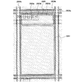
図1〜図2に、反射電極と透明電極とを形成する製造方法について述べる。
(Embodiment 1)
1 to 2 describe a manufacturing method for forming a reflective electrode and a transparent electrode.
まず、絶縁膜107の上にスパッタ法または印刷法またはCVD法またはインクジェット法などで導電膜106を形成する。導電膜106は、透明導電膜であっても反射性を有していても良い。透明導電膜である場合は、例えば、酸化インジウムに酸化スズを混ぜたインジウムスズ酸化物(ITO)膜、インジウムスズ酸化物(ITO)に酸化珪素を混ぜたインジウムスズ珪素酸化物(ITSO)膜、酸化インジウムに酸化亜鉛を混ぜたインジウム亜鉛酸化物(IZO)膜、酸化亜鉛膜、または酸化スズ膜、リンやボロンが含まれるシリコン(Si)などを用いることができる。なお、IZOとは、ITOに2〜20wt%の酸化亜鉛(ZnO)を混合させたターゲットを用いてスパッタリングにより形成される透明導電材料であるが、組成比などは、これに限定されない。
First, the
絶縁膜107上に導電膜106を形成し、続いて導電膜106上に導電膜105を積層する。導電膜106と導電膜105は連続的にスパッタで形成することができる。これにより、工程数を低減することが出来る。
A
導電膜105は、抵抗の低い材料や反射率が高い材料が好ましい。例えば、Ti、Mo、Ta、Cr、W、Al、Nd、Cu、Ag、Au、Pt、Nb、Si、Zn、Fe、Ba、Geなどやそれらの合金を用いることができる。また、これらを積層させた2層構造にしてもよい。その場合、Al(もしくはAlを主材料とした合金)と、Ti、Mo、Ta、Cr、Wなどの金属とを用いた2層積層構造としても良い。また、3層の積層構造でもよい。その場合、Al(もしくはAlを主材料とした合金)をTi、Mo、Ta、Cr、Wなどの金属で挟んだ3層積層構造としても良い。このように、Al(もしくはAlを主材料とした合金)の周りにTi、Mo、Ta、Cr、Wなどの金属を配置することにより、別の電極や配線に接続するときに、不具合を低減することができる。例えば、ITO膜などとAl(もしくはAlを主材料とした合金)を接続させると、電食などの不具合を起こすことがある。また、Si膜などとAl(もしくはAlを主材料とした合金)を接続させると、AlとSi膜とが反応してしまうことがある。これらは、多層構造にすることにより、低減することが出来る。
The
なお、導電膜としてITO膜を用いる場合は、ITO膜を熱処理して結晶化する工程が必要になってくる。そのときはITO膜をスパッタで形成し、焼成後、導電膜105を形成すると良い。ITSO膜を用いると、結晶化する工程が不要なため工程が少なくてすむ。
In the case where an ITO film is used as the conductive film, a process for crystallizing the ITO film by heat treatment is required. In that case, an ITO film may be formed by sputtering, and the
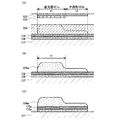
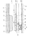
次いで、導電膜105上にレジスト膜104を全面に形成(塗布)した後、図1(A)に示す露光マスクを用いて露光を行う。
Next, after a resist
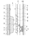
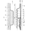
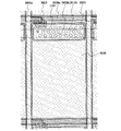
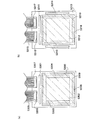
図1(A)において、露光マスクは、露光光が遮光される遮光部101aと、露光光が一部通過する半透部101bを有する。半透部101bには半透膜102が設けられ、露光光の光強度を低減させている。遮光部101aは半透膜102上に金属膜103が積層されて構成されている。遮光部101aの幅はt1、半透部101bの幅はt2と示す。ここでは半透部に半透膜を用いた例を示したが、これに限定されず、半透部は露光光の光強度を低減するものであればよい。また、半透部に回折格子パターンを用いてもよい。
In FIG. 1A, the exposure mask includes a light shielding portion 101a that shields exposure light and a semi-transmissive portion 101b through which part of the exposure light passes. The semi-transmissive portion 101b is provided with a
つまり、半透部にハーフトーンあるいはグレートーンと呼ばれるものを用いてもよい。 That is, what is called a halftone or a gray tone may be used for the semi-transmissive portion.
図1(A)に示す露光マスクを用いてレジスト膜の露光を行うと、非露光領域と露光領域が形成される。露光時には、光が遮光部101aで回り込んだり、半透部101bを通過することによって、露光領域が形成される。 When the resist film is exposed using the exposure mask shown in FIG. 1A, a non-exposed area and an exposed area are formed. At the time of exposure, an exposure region is formed by light traveling around the light shielding portion 101a or passing through the semi-transmissive portion 101b.
そして、現像を行うと、露光領域が除去されて、図1(B)に示すように、大きく分けて2つの膜厚を有するレジストパターン104aが導電膜105上に得られる。レジストパターン104aは膜厚の厚い領域と、該領域より膜厚の薄い領域とを有し、膜厚の薄い領域については、露光エネルギーまたは半透膜102の透過率を調節することで膜厚を調節することができる。
Then, when development is performed, the exposed region is removed, and a resist
次に、ドライエッチングにより導電膜105及び導電膜106のエッチングを行う。ドライエッチングはECR(Electron Cyclotron Resonance)やICP(Inductively Coupled Plasma)などの高密度プラズマ源を用いたドライエッチング装置によって行われる。
Next, the
すると、図1(C)に示すように、導電膜105a及び導電膜106aが形成される。
Then, as illustrated in FIG. 1C, a
なお、ここでは、ICP型エッチング装置を用いた例を示すが、これに限定されず、例えば、平行平板型エッチング装置、マグネトロン型エッチング装置、ECR型エッチング装置、ヘリコン型エッチング装置を用いてもよい。 Although an example using an ICP etching apparatus is shown here, the present invention is not limited to this. For example, a parallel plate etching apparatus, a magnetron etching apparatus, an ECR etching apparatus, or a helicon etching apparatus may be used. .
なお、導電膜105及び導電膜106のエッチングをウェットエッチングにより行っても良い。但し、微細加工にはドライエッチングが適しているため、ドライエッチングが好ましい。また、導電膜105及び導電膜106と、絶縁膜107との材料が大きく異なるため、ドライエッチングで行っても、導電膜105及び導電膜106と絶縁膜107とで大きなエッチング選択比がとれる。さらに両者のエッチング選択比を大きくするため、絶縁膜107の少なくとも最上層を窒化珪素膜で形成しても良い。
Note that the
こうして、図1(C)で示すように、絶縁膜107上に、導電膜106aと導電膜105aとの積層で構成されるパターンが形成される。
Thus, as illustrated in FIG. 1C, a pattern including a stack of the
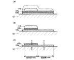
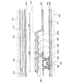
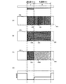
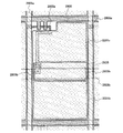
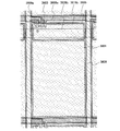
次に、レジストパターン104a(の一部)をアッシングまたはエッチングする(図2(A))。この工程により、レジストパターン104aの膜厚の薄い領域がエッチングされるとともに、その膜厚の薄い領域の膜厚分だけレジストパターン104aの全体の膜厚も薄くなる。そしてレジストパターン104bを形成する。レジストパターン104aは、膜厚方向だけでなく、幅方向もエッチングされるため、レジストパターン104bの幅は導電膜105a及び106aの幅よりも小さくなる。したがって、レジストパターン104bの側面は下層にある導電膜の側面と一致せず、レジストパターン104bの側面の方が後退している。図2(B)では、レジストパターン104bは左右非対称である。
Next, ashing or etching is performed on (a part of) the resist
次に、レジストパターン104bを用いて導電膜105aをエッチングし、導電膜105bを形成する(図2(B))。このとき同時に導電膜106aが無用にエッチングされないように、導電膜105aの材料は導電膜106aと高い選択比がとれるものが好ましい。例えば、その材料としてTi、Mo、Cr、Al、Nd等やその合金があり、これら材料でなる積層構造であっても良い。そして導電膜106aよりもパターンの小さい導電膜105bを形成する。
Next, the
図2(A)から図2(B)の導電膜105bのエッチングは、ドライエッチングで行ってもウェットエッチングで行っても良いが、図2ではドライエッチングの場合を図示する。導電膜105bは、側面がレジストパターン104bの側面と概ね一致するように形成される。導電膜105bは、一方の側面はレジストパターン104bの一方の側面の延長線上にあり、他方の側面はレジストパターン104bの他方の側面と一致する。
The etching of the
ドライエッチングを行うことにより、微細な加工が可能となる。ただし、導電膜105bを形成するときに、導電膜106aも一部がエッチングされる。
By performing dry etching, fine processing becomes possible. Note that part of the
一方、導電膜105bをウェットエッチングすると、等方的にエッチングが進むため、レジストパターン104bよりも小さい導電膜105bが形成される。レジストパターン104bの側面と導電膜105bの側面は一致しない。故に、同一のレジストパターン104bをマスクとしても、ドライエッチングよりウェットエッチングで形成したほうが、より小さい導電膜105bが形成される。
On the other hand, when the
ウェットエッチングを行うことにより、エッチングの選択比を十分大きくとることが可能となる。 By performing wet etching, the etching selectivity can be made sufficiently large.
なお、導電膜106aはドライエッチングで形成されるときは、その側面は、基板面に対してほぼ垂直または90度に近い角度θ1を有する。一方、導電膜105bがウェットエッチングで形成されると、等方的なエッチングにより、その側面は、基板面に対して鋭角な角度θ2を有する。したがって、導電膜106aと導電膜105bの側面の角度θ1と角度θ2を比較すると、θ1>θ2となっている。なお、角度θ1とは基板若しくは絶縁膜107の表面に対して導電膜106aの傾斜角度であり、角度θ2とは基板若しくは絶縁膜107の表面に対して導電膜105bの側面の傾斜角であり、θ1、θ2ともに0°〜90°の範囲内である。
Incidentally, when the
導電膜105bや導電膜106aが積層構造の場合は、各層によってエッチング速度が異なるときがある。これに伴い、基板面に対して各層の側面がなす角度もそれぞれ異なるときがある。したがってそのときは、基板面に対して最下層の膜の側面がなす角度をθ2とする。
In the case where the
なお、導電膜105b及び導電膜106aの側面がなだらかな面とならずに、凸凹を持つ場合がある。その場合、角度θ1及び角度θ2は適宜決定すればよい。例えば、凸凹した側面に対し大まかな直線または曲線を引き、それを用いて角度θ1及び角度θ2を決定することができる。また、凸凹した側面に基づき、複数の角度θ1及び角度θ2をとって、その平均値を角度θ1及び角度θ2とすることができる。最も合理的な方法を用いれば良い。
Note that the side surfaces of the
以上より、ドライエッチング法またはウェットエッチング法のいずれかのエッチング方法で導電膜105bを形成する。どちらのエッチング法で形成しても、導電膜106aの側面よりも後退した側面を有する導電膜105bが形成される。その要因の一つは、導電膜106aを形成するためのマスクであるレジストパターン104aと、導電膜105bを形成するためのマスクであるレジストパターン104bの大きさが異なり、レジストパターン104bのほうが小さいことである。
As described above, the
その後、レジストパターン104bを除去する(図2(C))。そして導電膜105b及び導電膜106aでなる電極が形成される。導電膜106aや導電膜105bは画素電極として機能する。ただし、これに限定されない。
Thereafter, the resist
より望ましくは、導電膜105bを反射導電膜とすることで、反射電極として機能させ、導電膜106aを透明導電膜とすることで、透明電極として機能させることである。そして、導電膜105bの下には、必ず導電膜106aが配置されており、導電膜105bの下面全体が導電膜106aの上面に接している。
More preferably, the
そして、反射部108aに反射電極を配置し、透過部108bに透明電極を配置する。これにより、反射電極と透明電極とを、少ない工程数で製造することが出来、半透過型表示装置を容易に製造することができる。また、反射電極や透明電極は、微細な加工を必要としない。多少、ずれていても、大きな問題はない。例えば、少し、反射電極が小さくて、透明電極が大きくても、表示に大きな影響を与えない。よって、このような製造方法を行っても、製造歩留まりが低下しにくい。よって、コスト低減や製造日数の短縮などに有益である。 A reflective electrode is disposed on the reflective portion 108a, and a transparent electrode is disposed on the transmissive portion 108b. Thereby, a reflective electrode and a transparent electrode can be manufactured with few processes, and a semi-transmissive display apparatus can be manufactured easily. Further, the reflective electrode and the transparent electrode do not require fine processing. Even if it is slightly off, there is no big problem. For example, even if the reflective electrode is small and the transparent electrode is large, the display is not greatly affected. Therefore, even if such a manufacturing method is performed, the manufacturing yield is unlikely to decrease. Therefore, it is useful for reducing costs and shortening the number of manufacturing days.
本発明の膜厚の異なる領域を有するレジストパターン104aを用いて、導電膜105b及び導電膜106aの積層を形成すると、導電膜105bを形成する際、つまりレジストパターン104bをマスクとしてエッチングをするときに、導電膜106a表面の一部は多少エッチングされる。特に、ドライエッチングにより導電膜105bを形成するときは、下層の導電膜106aと選択比がとりにくいので、より導電膜106a表面の一部はエッチングされやすい。そのため、図2(C)の導電膜106aの膜厚a(上面が導電膜105bと接する部分の導電膜106aの膜厚)と、膜厚b(上面が導電膜105bと接しない部分の導電膜106aの膜厚)を比較すると、膜厚a<膜厚bとなる。なお、膜厚aとは導電膜105bと重ならない部分における導電膜106aの平均膜厚を言い、膜厚bとは導電膜105bと重なる部分における導電膜106aの平均膜厚を言う。
When the
本実施の形態で形成する導電膜105bは、側面が傾斜する場合がある。そのため、液晶表示装置に利用した場合、導電膜105bの傾斜している側面側からラビングするようにすると、導電膜105bの側面においてスムーズにラビングを行うことができる。導電膜105bの側面が垂直である方向からラビングを行うと、垂直な側面部分でラビング布にストレスがかかる等の理由でラビングが不完全になり、配向が不完全になることがあった。したがって、ラビングは導電膜105bの側面が傾斜している側から行うことが好ましい。
The
また、ウェットエッチングにより、両側面ともに傾斜している導電膜105bを形成する場合は、どちらの方向からもスムーズにラビングでき、より効果的である。
In addition, when the
なお、図1(A)〜図1(B)で示したように、光が照射された部分のレジストが溶解する場合のレジストをポジ型レジストと呼ぶ。しかし、ポジ型レジストに限定されず、ネガ型レジストを用いても良い。ネガ型レジストは、光が照射されない部分のレジストが溶解するものである。 Note that, as shown in FIGS. 1A to 1B, a resist in a case where a resist in a portion irradiated with light is dissolved is referred to as a positive resist. However, the resist is not limited to a positive resist, and a negative resist may be used. In the negative resist, a portion of the resist not irradiated with light is dissolved.
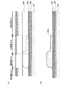
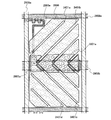
図3に、ネガ型レジストを用いた場合の図を示す。図1(A)が図3(A)に対応し、図1(B)が図3(B)に対応する。それ以外は、ネガ型とポジ型とでは、概ね違いはない。図3(A)に示すように、レジスト304で残したい部分には、透明部101cが配置され、レジスト304を除去したい部分には、遮光部101aが配置され、レジスト304を少し残したい部分には、半透部101bが配置される。その結果、図3(B)に示すように、レジスト304aが形成される。 FIG. 3 shows a diagram when a negative resist is used. 1A corresponds to FIG. 3A, and FIG. 1B corresponds to FIG. Other than that, there is almost no difference between the negative and positive types. As shown in FIG. 3A, the transparent portion 101c is disposed in the portion where the resist 304 is to be left, and the light-shielding portion 101a is disposed in the portion where the resist 304 is to be removed. The semi-transparent portion 101b is disposed. As a result, a resist 304a is formed as shown in FIG.
また、本実施の形態の中において、さまざまな図を用いて述べてきたが、1つの図は、様々な構成要件により成り立っている。したがって、各々の図の中から、各々の構成要件に関して、組み合わせて、さらなる構成を作ることも可能である。 Further, in the present embodiment, description has been made using various drawings, but one drawing is constituted by various components. Therefore, it is also possible to combine the components in the respective drawings to make further configurations.
(実施の形態2)
実施の形態1では、絶縁膜107の上に画素電極が形成される場合について述べた。しかし、実際には、画素電極は別の配線やトランジスタや保持容量などに接続されることになる。そのため、必要であれば、絶縁膜107にコンタクトホールを形成して、配線などと接続する必要がある。
(Embodiment 2)
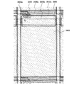
In
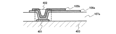
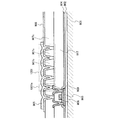
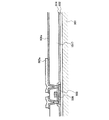
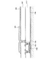
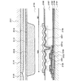
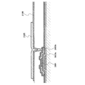
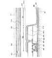
そこで、その場合の断面図を図4に示す。絶縁膜107aに、コンタクトホール402が形成されている。コンタクトホール402の下には、配線401が形成されている。配線401は、トランジスタのソースもしくはドレインの一方に接続される場合が多い。あるいは、配線401自体がトランジスタのソースもしくはドレインの一方であることも多い。また、保持容量の電極であることも多い。
FIG. 4 shows a cross-sectional view in that case. A
このとき、導電膜105bの下には、必ず導電膜106aが配置されている。これは、実施の形態1で述べた製造方法を用いるためである。よって、コンタクトホール402を覆って配置される導電膜106aの上にも、導電膜105bが配置されることになる。
At this time, the
そして、導電膜105bの下に、トランジスタや配線や保持容量が形成される。導電膜105bが反射電極であり、導電膜106aが透明電極である場合、透過領域を出来るだけ多くとることが望ましい。そこに光を透過させて表示を行うためである。一方、反射領域においては、反射電極の下に、何かが配置されていても、表示に影響が出ない。よって、導電膜105bの下に、トランジスタや配線や保持容量を配置することにより、効率的にレイアウトすることが出来る。
Then, a transistor, a wiring, and a storage capacitor are formed under the
なお、トランジスタや保持容量の全域が、反射電極の下に配置されていることが望ましいが、これに限定されない。トランジスタや保持容量について、各々の一部が反射電極の外側(反射領域の外側)に配置されていても問題ない。 Note that the entire region of the transistor and the storage capacitor is preferably disposed under the reflective electrode, but the present invention is not limited to this. There is no problem even if a part of each of the transistor and the storage capacitor is arranged outside the reflective electrode (outside the reflective region).
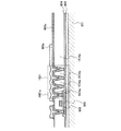
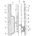
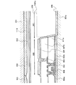
次に、反射電極の凹凸について述べる。反射電極は、外光を反射させて、表示を行うためのものである。反射電極に入ってきた外光を効率的に活用し、表示輝度を高めるためには、反射電極で乱反射させることが望ましい。 Next, the unevenness of the reflective electrode will be described. The reflective electrode reflects external light and performs display. In order to efficiently utilize the external light that has entered the reflective electrode and increase the display luminance, it is desirable to diffusely reflect the reflective electrode.
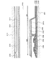
そこで、図5に示すように、絶縁膜107bに凹凸501を設けることにより、反射電極を凹凸にしてもよい。なお、絶縁膜107bは、積層構造になっていてもよい。また、図6に示すように、コンタクトホール501aも、凹凸を形成するための手段として用いても良い。この場合、コンタクトホール501aは、配線401と導電膜106aを接続させる機能も持っている。
Therefore, as shown in FIG. 5, the reflective electrode may be uneven by providing the insulating
次に、絶縁膜や反射電極の凹凸の形成方法の一例を示す。図1や図3では、露光光が遮光される遮光部101aと、露光光が一部通過する半透部101bを有する露光マスクを用いてレジストを形成する方法を述べた。そこでこの製造方法を、絶縁膜や反射電極の凹凸と、絶縁膜のコンタクトホールとを少ない工程数で形成する方法に適用してもよい。これにより、さらなる工程数の削減を実現することができる。 Next, an example of a method for forming the unevenness of the insulating film and the reflective electrode will be described. In FIG. 1 and FIG. 3, a method of forming a resist using an exposure mask having a light shielding portion 101 a that shields exposure light and a semi-transmissive portion 101 b through which the exposure light partially passes has been described. Therefore, this manufacturing method may be applied to a method of forming the unevenness of the insulating film or the reflective electrode and the contact hole of the insulating film with a small number of steps. Thereby, the reduction of the further number of processes is realizable.
また、透明電極と反射電極とを形成する部分で、この製造方法を用いているため、製造設備が整っている。そのため、さらに、絶縁膜や反射電極の凹凸の形成のために、この製造方法を用いても、特別に必要なものがない。よって、両方ともこの製造方法を用いて形成することに、非常に大きなメリットがある。 Moreover, since this manufacturing method is used in the portion where the transparent electrode and the reflective electrode are formed, the manufacturing equipment is in place. Therefore, even if this manufacturing method is used for forming the unevenness of the insulating film and the reflective electrode, there is nothing specially necessary. Therefore, both have a great advantage in forming using this manufacturing method.
この凹凸も、形状が多少ずれていても問題ない。微細化を強く要請されるような部分ではない。よって、製造歩留まりを低下させることなく、製造することが出来る。 This unevenness is not a problem even if the shape is slightly deviated. This is not the part that strongly demands miniaturization. Therefore, it can manufacture without reducing a manufacturing yield.
図7(A)において、露光マスクは、露光光が遮光される遮光部701aと、露光光が一部通過する半透部701bと、露光光が通過する透明部701cを有する。半透部701bには半透膜702が設けられ、露光光の光強度を低減させている。遮光部701aは半透膜702上に金属膜703が積層されて構成されている。ここでは半透部に半透膜を用いた例を示したが、これに限定されず、半透部は露光光の光強度を低減するものであればよい。また、半透部に回折格子パターンを用いてもよい。
In FIG. 7A, the exposure mask includes a light-shielding
絶縁膜707の上に電極705が配置されている。その上に光によって感光する膜(例えば、感光性のアクリルなど)704を配置する。図7(A)に示す露光マスクを用いて膜704の露光を行うと、非露光領域と露光領域と半露光領域が形成される。そして、光が当たった部分は、膜704が除去される。すると、図7(B)に示すように、膜704aのようになり、コンタクトホール706aと凹凸706とが同時に形成される。
An
なお、図7では、コンタクトホールの他に凹凸を形成したが、これに限定されない。コンタクトホールのような孔を複数形成し、これにより、凹凸を形成してもよい。その場合、その孔の下側には、配線を設けなくても良い。なぜなら、電気的に接続させることが目的ではないからである。ただし、電気的に問題がない場合であれば、配線を設けても良い。 In FIG. 7, irregularities are formed in addition to the contact holes, but the present invention is not limited to this. A plurality of holes such as contact holes may be formed, whereby unevenness may be formed. In that case, it is not necessary to provide wiring under the hole. This is because it is not intended to be electrically connected. However, if there is no electrical problem, wiring may be provided.
なお、図7では、光が当たった部分の膜704が除去されたが、これに限定されない。逆に、光が当たらなかった部分の膜704が除去されるようにしてもよい。
Note that in FIG. 7, the
なお、図7では、レジストを用いなかったが、これに限定されない。膜を形成したあと、レジストを用いて、ドライエッチングやウェットエッチングを行って、凹凸やコンタクトホールを形成してもよい。 In FIG. 7, no resist is used, but the present invention is not limited to this. After the film is formed, unevenness and contact holes may be formed by performing dry etching or wet etching using a resist.
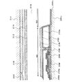
なお、透過領域では、反射領域よりも、液晶の厚さ(セルギャップ)を厚くする場合がある。これは、反射領域では、光が往復して通るが、透過領域では、光が一度通るだけだからである。そこで、セルギャップを調節して、透過領域でのセルギャップを厚くするようにしてもよい。その場合の図を図8に示す。膜704を除去して膜704bを形成することによって、コンタクトホールだけでなく、透過領域における凹部801を形成することが出来る。凹部801の部分は、セルギャップが厚くなる。よって、この部分を透過領域にすればよい。
In the transmissive region, the liquid crystal may have a greater thickness (cell gap) than the reflective region. This is because light passes back and forth in the reflection region, but only passes once in the transmission region. Therefore, the cell gap may be adjusted to increase the cell gap in the transmission region. The figure in that case is shown in FIG. By removing the
この場合、セルギャップを厚くするために、特別な工程の増加が必要ないため、コストを低くすることが出来る。 In this case, since it is not necessary to increase the number of special processes in order to increase the cell gap, the cost can be reduced.
なお、本実施の形態は、実施の形態1で述べた内容を、一部変形した場合の一例を示している。したがって、実施の形態1で述べた内容は、本実施の形態にも適用することができるし、本実施の形態と組み合わせることも出来る。
Note that this embodiment shows an example in which the content described in
また、本実施の形態の中において、さまざまな図を用いて述べてきたが、1つの図は、様々な構成要件により成り立っている。したがって、各々の図の中から、各々の構成要件に関して、組み合わせて、さらなる構成を作ることも可能である。 Further, in the present embodiment, description has been made using various drawings, but one drawing is constituted by various components. Therefore, it is also possible to combine the components in the respective drawings to make further configurations.
(実施の形態3)
次に、トランジスタを配置した場合の具体例について述べる。ただし、トランジスタは必ずしも必要ではなく、いわゆるパッシブマトリックス型に適用してもよい。
(Embodiment 3)
Next, a specific example in which a transistor is arranged will be described. However, the transistor is not necessarily required and may be applied to a so-called passive matrix type.
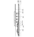
まず、図9を用いて、基板901上にトップゲート型のTFTを形成する方法を説明する。基板901は透光性を有する基板、例えば石英基板、ガラス基板またはプラスチック基板である。なお、基板901は遮光性の基板でもよく、半導体基板、SOI(Silicon on Insulator)基板でもよい。
First, a method for forming a top gate type TFT on a
基板901上に下地膜として絶縁膜902を成膜する。絶縁膜902としては、酸化シリコン膜、窒化シリコン膜または酸化窒化シリコン膜(SiOxNy)等の絶縁膜の単層、或いはこれらの膜の少なくとも2つの膜でなる積層を用いる。
An insulating
なお、半導体と接する部分では、酸化シリコン膜を用いる方がよい。その結果、下地膜における電子のトラップやトランジスタ特性のヒステリシスを抑えることが出来る。また、下地膜として、窒素を多く含む膜を少なくとも1つ配置することが望ましい。それにより、ガラスからの不純物を低減することが出来る。 Note that a silicon oxide film is preferably used in a portion in contact with the semiconductor. As a result, electron trapping in the base film and hysteresis of transistor characteristics can be suppressed. Further, it is desirable to dispose at least one film containing a large amount of nitrogen as the base film. Thereby, impurities from the glass can be reduced.
次いで、絶縁膜902上に島状半導体膜903を形成する。
Next, an island-shaped
島状半導体膜903は、絶縁膜902上にスパッタ法、LPCVD法、またはプラズマCVD法等により半導体膜を全面に形成した後、フォトリソグラフィ法等により形成されたマスクを用いて半導体膜を形状加工して形成する。島状半導体膜903を結晶性半導体膜で形成するときは、基板901上に直接結晶性半導体膜を形成する方法と、非晶質半導体膜を基板901上に形成した後に、加熱処理により結晶化させて結晶性半導体膜を形成する方法がある。後者の方法において、結晶化の際の加熱処理は、加熱炉、レーザ照射、若しくはレーザ光の代わりにランプから発する光の照射(以下、ランプアニールと表記する)、又はそれらを組み合わせて用いることにより行われる。
The island-shaped
また、ニッケルなどを非晶質半導体膜に添加した後に上記加熱処理を行う熱結晶化法により結晶性半導体膜を形成してもよい。なお、ニッケルを用いた熱結晶化法を用いて結晶化を行って結晶性半導体膜を得た場合は、結晶化後にニッケルを除去するゲッタリング処理を行うことが好ましい。 Alternatively, the crystalline semiconductor film may be formed by a thermal crystallization method in which the heat treatment is performed after nickel or the like is added to the amorphous semiconductor film. Note that in the case where a crystalline semiconductor film is obtained by performing crystallization using a thermal crystallization method using nickel, it is preferable to perform gettering treatment for removing nickel after crystallization.
レーザ照射により結晶化して結晶性半導体膜を作製する場合には、連続発振(CW:continuous−wave)型のレーザビームやパルス発振型のレーザビーム(パルスレーザビーム)を用いることができる。ここで用いることができるレーザビームは、Arレーザ、Krレーザ、エキシマレーザなどの気体レーザ、単結晶のYAG、YVO4、フォルステライト(Mg2SiO4)、YAlO3、GdVO4、若しくは多結晶(セラミック)のYAG、Y2O3、YVO4、YAlO3、GdVO4に、ドーパントとしてNd、Yb、Cr、Ti、Ho、Er、Tm、Taのうち1種または複数種添加されているものを媒質とするレーザ、ガラスレーザ、ルビーレーザ、アレキサンドライトレーザ、Ti:サファイアレーザ、銅蒸気レーザまたは金蒸気レーザのうち一種または複数種から発振されるものを用いることができる。このようなレーザビームの基本波、及びこれらの基本波の第2高調波から第4高調波のレーザビームを照射することで、大粒径の結晶を得ることができる。例えば、Nd:YVO4レーザ(基本波1064nm)の第2高調波(532nm)や第3高調波(355nm)を用いることができる。このレーザは、CWで射出することも、パルス発振で射出することも可能である。CWで射出する場合は、レーザのパワー密度は0.01〜100MW/cm2程度(好ましくは0.1〜10MW/cm2)必要である。そして、走査速度を10〜2000cm/sec程度として照射する。 In the case of manufacturing a crystalline semiconductor film by crystallization by laser irradiation, a continuous-wave (CW) laser beam or a pulsed laser beam (pulse laser beam) can be used. The laser beam that can be used here is a gas laser such as an Ar laser, a Kr laser, or an excimer laser, single crystal YAG, YVO 4 , forsterite (Mg 2 SiO 4 ), YAlO 3 , GdVO 4 , or polycrystalline ( (Ceramics) YAG, Y 2 O 3 , YVO 4 , YAlO 3 , GdVO 4 with one or more of Nd, Yb, Cr, Ti, Ho, Er, Tm, Ta added as dopants A laser oscillated from one or more of laser, glass laser, ruby laser, alexandrite laser, Ti: sapphire laser, copper vapor laser, or gold vapor laser as a medium can be used. By irradiating the fundamental wave of such a laser beam and the second to fourth harmonic laser beams of these fundamental waves, a crystal having a large grain size can be obtained. For example, a second harmonic (532 nm) or a third harmonic (355 nm) of an Nd: YVO 4 laser (fundamental wave 1064 nm) can be used. This laser can be emitted by CW or pulsed oscillation. When injected at a CW, the power density of the laser is about 0.01 to 100 MW / cm 2 (preferably 0.1 to 10 MW / cm 2) is required. Then, irradiation is performed at a scanning speed of about 10 to 2000 cm / sec.
なお、単結晶のYAG、YVO4、フォルステライト(Mg2SiO4)、YAlO3、GdVO4、若しくは多結晶(セラミック)のYAG、Y2O3、YVO4、YAlO3、GdVO4に、ドーパントとしてNd、Yb、Cr、Ti、Ho、Er、Tm、Taのうち1種または複数種添加されているものを媒質とするレーザ、Arイオンレーザ、またはTi:サファイアレーザは、連続発振をさせることが可能であり、Qスイッチ動作やモード同期などを行うことによって10MHz以上の発振周波数でパルス発振をさせることも可能である。10MHz以上の発振周波数でレーザビームを発振させると、半導体膜がレーザによって溶融してから固化するまでの間に、次のパルスが半導体膜に照射される。従って、発振周波数が低いパルスレーザを用いる場合と異なり、半導体膜中において固液界面を連続的に移動させることができるため、走査方向に向かって連続的に成長した結晶粒を得ることができる。 Note that single crystal YAG, YVO 4 , forsterite (Mg 2 SiO 4 ), YAlO 3 , GdVO 4 , or polycrystalline (ceramic) YAG, Y 2 O 3 , YVO 4 , YAlO 3 , GdVO 4 , dopants Nd, Yb, Cr, Ti, Ho, Er, Tm, Ta, a laser using a medium added with one or more, an Ar ion laser, or a Ti: sapphire laser should oscillate continuously It is also possible to perform pulse oscillation at an oscillation frequency of 10 MHz or more by performing Q switch operation, mode synchronization, or the like. When the laser beam is oscillated at an oscillation frequency of 10 MHz or more, the semiconductor film is irradiated with the next pulse during the period from when the semiconductor film is melted by the laser to solidification. Therefore, unlike the case of using a pulse laser having a low oscillation frequency, the solid-liquid interface can be continuously moved in the semiconductor film, so that crystal grains continuously grown in the scanning direction can be obtained.
媒質としてセラミック(多結晶)を用いると、短時間かつ低コストで自由な形状に媒質を形成することが可能である。単結晶を用いる場合、通常、直径数mm、長さ数十mmの円柱状の媒質が用いられているが、セラミックを用いる場合はさらに大きいものを作ることが可能である。 When ceramic (polycrystal) is used as the medium, it is possible to form the medium in a free shape in a short time and at low cost. When a single crystal is used, a cylindrical medium having a diameter of several millimeters and a length of several tens of millimeters is usually used. However, when ceramic is used, a larger one can be made.
発光に直接寄与する媒質中のNd、Ybなどのドーパントの濃度は、単結晶中でも多結晶中でも大きくは変えられないため、濃度を増加させることによるレーザの出力向上にはある程度限界がある。しかしながら、セラミックの場合、単結晶と比較して媒質の大きさを著しく大きくすることができるため大幅な出力向上を図ることができる。 Since the concentration of dopants such as Nd and Yb in the medium that directly contributes to light emission cannot be changed greatly regardless of whether it is a single crystal or a polycrystal, there is a certain limit to improving the laser output by increasing the concentration. However, in the case of ceramic, since the size of the medium can be remarkably increased as compared with the single crystal, the output can be greatly improved.
さらに、セラミックの場合では、平行六面体形状や直方体形状の媒質を容易に形成することが可能である。このような形状の媒質を用いて、発振光を媒質の内部でジグザグに進行させると、発振光路を長くとることができる。そのため、増幅が大きくなり、大出力で発振させることが可能になる。また、このような形状の媒質から射出されるレーザビームは射出時の断面形状が四角形状であるため、丸状のビームと比較すると、線状ビームに整形するのに有利である。このように射出されたレーザビームを、光学系を用いて整形することによって、短辺の長さ1mm以下、長辺の長さ数mm〜数mの線状ビームを容易に得ることが可能となる。また、励起光を媒質に均一に照射することにより、線状ビームは長辺方向にエネルギー分布の均一なものとなる。 Further, in the case of ceramic, a medium having a parallelepiped shape or a rectangular parallelepiped shape can be easily formed. When a medium having such a shape is used to cause oscillation light to travel in a zigzag manner inside the medium, the oscillation optical path can be made longer. As a result, amplification is increased and oscillation can be performed with high output. Further, since the laser beam emitted from the medium having such a shape has a quadrangular cross-sectional shape at the time of emission, it is advantageous for shaping into a linear beam as compared with a round beam. By shaping the emitted laser beam using an optical system, it is possible to easily obtain a linear beam having a short side length of 1 mm or less and a long side length of several mm to several m. Become. In addition, by irradiating the medium with the excitation light uniformly, the linear beam has a uniform energy distribution in the long side direction.
この線状ビームを半導体膜に照射することによって、半導体膜の全面をより均一にアニールすることが可能になる。線状ビームの両端まで均一なアニールが必要な場合は、その両端にスリットを配置し、エネルギーの減衰部を遮光するなどの工夫が必要となる。 By irradiating the semiconductor film with this linear beam, the entire surface of the semiconductor film can be annealed more uniformly. When uniform annealing is required up to both ends of the linear beam, it is necessary to arrange a slit at both ends to shield the energy attenuating portion.
このようにして得られた強度が均一な線状ビームを用いて半導体膜をアニールし、この半導体膜を用いて電子機器を作製すると、その電子機器の特性は、良好かつ均一である。 When a semiconductor film is annealed using a linear beam having a uniform intensity obtained in this manner and an electronic device is manufactured using this semiconductor film, the characteristics of the electronic device are good and uniform.
次いで、必要があればTFTのしきい値を制御するために微量な不純物元素(ボロンまたはリン)のドーピングを半導体層に対して行う。ここでは、ジボラン(B2H6)を質量分離しないでプラズマ励起したイオンドープ法を用いる。ただし、質量分離して、ドープ量を正確に制御するようにしてもよい。これにより、しきい値電圧を正確に制御出来る。 Next, if necessary, a small amount of impurity element (boron or phosphorus) is doped into the semiconductor layer in order to control the threshold value of the TFT. Here, an ion doping method in which diborane (B 2 H 6 ) is plasma-excited without mass separation is used. However, the amount of dope may be accurately controlled by mass separation. Thereby, the threshold voltage can be accurately controlled.
この島状半導体膜903の厚さは25〜80nm(好ましくは30〜70nm)の厚さで形成する。半導体膜の材料に限定はないが、好ましくはシリコンまたはシリコンゲルマニウム(SiGe)合金などで形成すると良い。
The island-shaped
そして、島状半導体膜903を覆うようにゲート絶縁膜904を形成する。ゲート絶縁膜904としては、熱酸化膜、酸化シリコン膜、窒化シリコン膜または酸化窒化シリコン膜などの単層または積層構造を用いることができる。島状半導体膜903と接するゲート絶縁膜は酸化珪素膜が好ましい。それは、酸化珪素膜にすると島状半導体膜との界面におけるトラップ準位が少なくなるからである。また、ゲート電極をMoで形成するときは、ゲート電極と接するゲート絶縁膜は窒化シリコン膜が好ましい。それは、窒化シリコン膜はMoを酸化させないからである。
Then, a
ここではゲート絶縁膜904として、プラズマCVD法により厚さ115nmの酸化窒化シリコン膜(組成比Si=32%、O=59%、N=7%、H=2%)を形成する。
Here, a 115-nm-thick silicon oxynitride film (composition ratio: Si = 32%, O = 59%, N = 7%, H = 2%) is formed as the
次に、ゲート絶縁膜904上に導電層を形成して、フォトリソグラフィ法等により形成したマスクを用いて導電層を形状加工し、ゲート電極908やゲート配線を形成する。保持容量用の配線や電極を形成することもある。これらの導電層の材料としてはTi、Mo、Ta、Cr、W、Al、Nd、Cu、Ag、Au、Pt、Nb、Si、Zn、Fe、Ba、Geなどや、これら元素の合金等がある。もしくは、これら元素またはこれら元素の合金の積層により構成しても良い。ここではMoによりゲート電極を形成する。Moは、エッチングしやすく、熱に強いので好適である。次に、ゲート電極908またはレジストをマスクとして島状半導体膜903に不純物元素をドーピングし、チャネル形成領域と、ソース領域及びドレイン領域となる不純物領域とを形成する。
Next, a conductive layer is formed over the
このとき、LDD領域を形成してもよい。 At this time, an LDD region may be formed.
次いで、透光性を有する無機材料(酸化シリコン、窒化シリコン、酸化窒化シリコンなど)または、低誘電率の有機化合物材料(感光性又は非感光性の有機樹脂材料)やそれらの積層を用いて絶縁膜917を形成する。また、シロキサンを含む材料を用いて絶縁膜917(もしくはその一部)を形成してもよい。なお、シロキサンは、シリコン(Si)と酸素(O)との結合で骨格構造が構成される材料である。置換基として、少なくとも水素を含む有機基(例えばアルキル基、芳香族炭化水素)が用いられる。置換基としてフルオロ基を用いてもよい。または置換基として、少なくとも水素を含む有機基と、フルオロ基とを用いてもよい。絶縁膜917は積層構造でも良い。
Next, insulation is performed using a light-transmitting inorganic material (silicon oxide, silicon nitride, silicon oxynitride, or the like), a low dielectric constant organic compound material (photosensitive or non-photosensitive organic resin material), or a laminate thereof. A
次いで、フォトマスクを用いてレジストからなるマスクを形成し、そのマスクを用いて、絶縁膜917、及びゲート絶縁膜904を選択的にエッチングし、コンタクトホールを形成する。そして、レジストからなるマスクを除去する。
Next, a resist mask is formed using a photomask, and the insulating
そして、絶縁膜917上にスパッタ法または印刷法またはCVD法またはインクジェット法で導電膜を形成する。そして、フォトリソグラフィ法等により形成したマスクを用いて導電層を形状加工し、ドレイン電極909やソース電極やソース配線を形成する。材料としてはTi、Mo、Ta、Cr、W、Al、Nd、Cu、Ag、Au、Pt、Nb、Si、Zn、Fe、Ba、Geなどや、これら元素の合金等がある。もしくは、これら元素またはこれら元素の合金の積層によりドレイン電極909などを構成しても良い。ここではAlの上下をMoで挟んだ三層構造によりドレイン電極やソース配線を形成する。
Then, a conductive film is formed over the insulating
このドレイン電極909が、図4、図6における配線401、図7、図8における電極705に相当する。
The
その上に、絶縁膜907を形成する。絶縁膜907は、平坦性や被覆性が良いと望ましいため、有機材料を用いて形成されることが多い。なお、無機材料(酸化シリコン、窒化シリコン、酸化窒化シリコンなど)の上に、有機材料が形成され、多層構造になっていてもよい。この絶縁膜907が、図1〜図3などにおける絶縁膜107に相当する。
An insulating
そして、絶縁膜907にコンタクトホールを形成したあと、上にスパッタ法または印刷法またはCVD法またはインクジェット法で導電膜を形成する。
Then, after forming a contact hole in the insulating
図9における導電膜906が、図2(C)、図4〜図6の導電膜106aに相当する。そして、図9における導電膜905が、図2(C)、図4〜図6の導電膜105bに相当する。
A
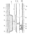
導電膜906は、画素電極の一部であり、光を透過する透明電極である。そして、導電膜905は、画素電極の一部であり、光を反射する反射電極である。反射電極の下面全体が透明電極の上面に接している。
The
透明電極の場合は、例えば、酸化インジウムに酸化スズを混ぜたインジウムスズ酸化物(ITO)膜、インジウムスズ酸化物(ITO)に酸化珪素を混ぜたインジウムスズ珪素酸化物(ITSO)膜、酸化インジウムに酸化亜鉛を混ぜたインジウム亜鉛酸化物(IZO)膜、酸化亜鉛膜、または酸化スズ膜などを用いることができる。なお、IZOとは、ITOに2〜20wt%の酸化亜鉛(ZnO)を混合させたターゲットを用いてスパッタリングにより形成される透明導電材料であるが、これに限定されない。 In the case of the transparent electrode, for example, an indium tin oxide (ITO) film in which tin oxide is mixed with tin oxide, an indium tin silicon oxide (ITSO) film in which silicon oxide is mixed in indium tin oxide (ITO), indium oxide An indium zinc oxide (IZO) film, a zinc oxide film, a tin oxide film, or the like in which zinc oxide is mixed can be used. Note that IZO is a transparent conductive material formed by sputtering using a target in which 2 to 20 wt% of zinc oxide (ZnO) is mixed with ITO, but is not limited thereto.
反射電極の場合は、例えば、Ti、Mo、Ta、Cr、W、Al、Nd、Cu、Ag、Au、Pt、Nb、Si、Zn、Fe、Ba、Geなどやそれらの合金などを用いることができる。また、Ti、Mo、Ta、Cr、WとAlを積層させた2層構造、AlをTi、Mo、Ta、Cr、Wなどの金属で挟んだ3層積層構造としても良い。 In the case of a reflective electrode, for example, Ti, Mo, Ta, Cr, W, Al, Nd, Cu, Ag, Au, Pt, Nb, Si, Zn, Fe, Ba, Ge, or an alloy thereof is used. Can do. Alternatively, a two-layer structure in which Ti, Mo, Ta, Cr, W, and Al are stacked, or a three-layer structure in which Al is sandwiched between metals such as Ti, Mo, Ta, Cr, and W may be used.
導電膜905、導電膜906は、実施の形態1〜実施の形態2で述べた方法を用いて形成する。
The
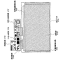
導電膜905、導電膜906の上には、図示していないが、配向膜が形成されている場合が多い。
Although not illustrated, an alignment film is often formed over the
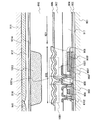
対向基板911には、カラーフィルタ916やブラックマトリックス915や平坦化膜912や対向電極914などが形成されている。対向基板911と基板901の間に、液晶層910が配置されている。
On the
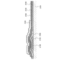
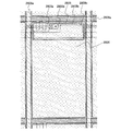
なお、光を反射させて表示を行う部分(反射部)920においては、液晶層910の中を光が2回通る。つまり、外光が対向基板側から液晶層910に入射し、導電膜905で反射されて、再度、液晶層910を通過し、対向基板側から出て行くので、液晶層910を2回通ることになる。
Note that light passes through the
一方、光を透過させて表示を行う部分(透過部)921においては、光は、導電膜906を通って液晶層910に入り、対向基板から出て行く。つまり、液晶層910の中を光が1回通る。
On the other hand, in a portion (transmission portion) 921 that transmits light and performs display, the light enters the
ここで、液晶層910は、屈折率異方性を有しているため、液晶層910を通る距離によって、光の偏光状態が変わってくる。そのため、画像を表示する場合に、正しく表示できなくなってしまう。そこで、光の偏光状態を調整する必要がある。そのための方法として、光を反射させて表示を行う部分(反射部)920の液晶層910の厚さ(いわゆるセルギャップ)を薄くすることにより、2回通っても、距離が長くなりすぎないようにすればよい。
Here, since the
そこで、液晶層910の厚さ(いわゆるセルギャップ)を薄くするために、厚さを調整する膜(セルギャップを調整するための膜、厚さ調整膜又はセルギャップ調整膜などともいう)を配置すればよい。図9においては、絶縁膜913がそれに相当する。つまり、光を反射させて表示を行う部分(反射部)920において、絶縁膜913は液晶層の厚さを調整する為に設けられている層である。絶縁膜913を設けることによって反射部920における液晶層の厚さを、透過部921における液晶層の厚さよりも薄くすることが出来る。
Therefore, in order to reduce the thickness of the liquid crystal layer 910 (so-called cell gap), a film for adjusting the thickness (also referred to as a film for adjusting the cell gap, a thickness adjusting film, or a cell gap adjusting film) is disposed. do it. In FIG. 9, the insulating
なお、反射部920での液晶層910の厚さは、透過部921における液晶層910の厚さの2分の1となることが望ましい。ここで、2分の1とは、人間の目で視認できない程度のずれを有していても良い程度のずれ量も含む。
Note that the thickness of the
ただし、光は基板と垂直な方向、つまり法線方向のみから入射するわけではない。斜めから入射する場合も多い。よって、それらの場合を総合して、反射部920と透過部921とで、光の通る距離が実質的に、概ね同じ程度になればよい。したがって、反射部920での液晶層910の厚さは、透過部921における液晶層910の厚さの概ね3分の1以上、3分の2以下となることが望ましい。
However, light does not enter only from the direction perpendicular to the substrate, that is, the normal direction. In many cases, it is incident obliquely. Therefore, in total, it is only necessary that the distance that the light passes between the reflecting
このように、厚さを調整する膜は対向基板911側に配置することにより、形成が容易になる。厚さを調整する膜は、アクリルやポリイミドなどの有機材料を用いて形成されることが好適である。
In this manner, the film for adjusting the thickness can be easily formed by disposing the film on the
なお、厚さを調整する膜に、光散乱用粒子が混在されていてもよい。これにより、光を散乱させ、輝度を向上させることが出来る。光散乱用粒子は、セルギャップ調整膜とは異なる屈折率を有する材質で出来ており、透光性を有する樹脂材料から成る。このような光散乱用粒子を、セルギャップを調整するための膜に混在させて、作製すればよい。 Note that light scattering particles may be mixed in the film for adjusting the thickness. Thereby, light can be scattered and a brightness | luminance can be improved. The light scattering particles are made of a material having a refractive index different from that of the cell gap adjusting film and are made of a resin material having translucency. Such light scattering particles may be produced by mixing them in a film for adjusting the cell gap.
なお、対向電極914は、絶縁膜913の上(液晶層910に近い側)にあることが望ましい。それにより、液晶層910に十分大きな電界を加えることが出来る。
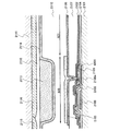
Note that the
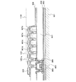
ただし、これに限定されない。図10に示すように、電極1014の上(液晶層910に近い側)に絶縁膜1013を配置してもよい。絶縁膜1013は非常に厚いため、電極1014が断線してしまうことを防止することが出来る。
However, it is not limited to this. As illustrated in FIG. 10, an insulating
なお、図9では、反射部920において、反射電極に凹凸が形成されていなかったが、図5,図6に示すように、凹凸を形成してもよい。その場合を図10に示す。凹凸は、図7で述べた方法を用いて形成してもよい。凹凸1001やコンタクトホール1001aにより、光を拡散させることが出来る。
In FIG. 9, the
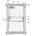
なお、図9、図10では、厚さ調整膜は対向基板側に設けられていたが、これに限定されない。トランジスタが形成されている側に配置してもよい。その場合を図11に示す。絶縁膜907aの一部が除去されて、形成されている。なお、図10と図11とを組み合わせてもよい。その場合の一例を図12に示す。凹部1101は、図8の凹部801に対応する。このように、透過部921に凹部801を設けることにより、透過部921のセルギャップを反射部920のセルギャップよりも大きくすることが出来る。
9 and 10, the thickness adjusting film is provided on the counter substrate side, but the present invention is not limited to this. You may arrange | position to the side in which the transistor is formed. This case is shown in FIG. A part of the insulating
なお、凹部と厚さ調整膜とを両方設けても良い。両方で厚さを制御すればよいので、片方の厚さは、あまり大きくなくても良い。そのため、製造しやすくなる。 Note that both the recess and the thickness adjusting film may be provided. Since the thickness may be controlled by both, the thickness of one side does not have to be very large. Therefore, it becomes easy to manufacture.
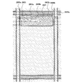
なお、図11において、凹部1101は、絶縁膜907aの一部が除去されて、形成されているが、これに限定されない。他の絶縁膜も除去されてもよい。例えば、図50には、絶縁膜907aだけでなく、絶縁膜917aの一部も除去されている場合を示す。これにより、反射部920と透過部921とで、セルギャップの差を付けやすくなる。また、絶縁膜907aだけを除去する場合と比較して、絶縁膜907aの厚さを薄くすることが出来る。そのため、基板のそりなどの不具合を低減することが出来る。
In FIG. 11, the
図51には、さらに、絶縁膜902e、ゲート絶縁膜904e、基板901eなども一部を除去している場合を示す。絶縁膜902e、ゲート絶縁膜904e、基板901eなどは、成分が類似した膜で形成されている場合があるため、凹部1101cをより深く形成することが出来る。
FIG. 51 shows the case where some of the insulating
なお、凹凸は、コンタクトホールを用いて形成してもよい。その場合を図13に示す。導電膜906がドレイン電極909に接続されていない場所にコンタクトホール1301を設けて、それを用いて凹凸を形成している。このように、配線と配線とを接続させるためではなく、配線や電極の表面を凹凸にするために、複数のコンタクトホール1301を形成している。なお、コンタクトホール1301において、コンタクトホール1001aと同様に、導電膜906をドレイン電極909と接続させるようにしてもよい。
Note that the unevenness may be formed using a contact hole. Such a case is shown in FIG. A
また、図14に、図13の場合に凹部1101を設けた場合を示す。
FIG. 14 shows a case where the
このように、凹凸の有無、凹凸の形成方法、セルギャップの調整方法(厚さ調整を対向基板側で行うか、TFT基板側で行うか)などは、各々の方式が複数ある。よって、そのいずれかを選択して、組み合わせて良い。 As described above, there are a plurality of methods for the presence / absence of unevenness, a method for forming unevenness, and a method for adjusting a cell gap (whether thickness adjustment is performed on the counter substrate side or the TFT substrate side). Therefore, any one of them may be selected and combined.
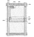
なお、導電膜905が反射電極の場合、その下に、トランジスタや配線や保持容量が形成されることが望ましい。導電膜905が反射電極であり、導電膜906が透明電極である場合、透過領域を出来るだけ多くとることが望ましい。そこに光を透過させて表示を行うためである。一方、反射領域においては、反射電極の下に、何かが配置されていても、表示に影響が出ない。よって、導電膜905の下に、トランジスタや配線や保持容量を配置することにより、効率的にレイアウトすることが出来る。
Note that in the case where the
なお、トランジスタや保持容量の全域が、反射電極の下に配置されていることが望ましいが、これに限定されない。トランジスタや保持容量について、各々の一部が反射電極の外側(反射領域の外側)に配置されていても問題ない。 Note that the entire region of the transistor and the storage capacitor is preferably disposed under the reflective electrode, but the present invention is not limited to this. There is no problem even if a part of each of the transistor and the storage capacitor is arranged outside the reflective electrode (outside the reflective region).
そこで、反射電極の下にトランジスタや保持容量を配置した場合の断面図を図47,図48に示す。図47では、トランジスタ4702で活性層として用いる半導体層の一部を用いて、保持容量4701の電極の1つを構成している。図47では、島状半導体膜903と、保持容量用配線908eの間で、ゲート絶縁膜904を絶縁物として、保持容量4701を形成している。また、ドレイン電極909の一部を用いて、保持容量用配線908eとの間でも、絶縁膜917を絶縁物として、保持容量4701を形成している。図48では、トランジスタ4702で活性層として用いる半導体層とは別の半導体層903fと、保持容量用配線908fとの間で、ゲート絶縁膜904を絶縁物として、保持容量4801を形成している。半導体層903fは、コンタクトホールを介して、ドレイン電極909と接続されている。
Therefore, FIGS. 47 and 48 are cross-sectional views in the case where a transistor and a storage capacitor are arranged under the reflective electrode. In FIG. 47, part of a semiconductor layer used as an active layer in the
なお、図9〜図14、図47〜図48までにおいて、ドレイン電極の上に絶縁膜を設けていたが、これに限定されない。ドレイン電極905aを反射電極とし、ドレイン電極の下に透明電極906aを配置し、ゲート電極の上の絶縁膜1517の上に、画素電極を配置してもよい。その場合の断面図を図15に示す。なお、図15の場合においても、反射電極の表面を凹凸にしてもいいし、セルギャップを調整するため、厚さ調整膜や凹部を構成してもよい。一例として、コンタクトホール1601、1601aを用いて、反射電極の凹凸を形成した場合を図16に示す。
9 to 14 and 47 to 48, the insulating film is provided on the drain electrode. However, the present invention is not limited to this. The
なお、図9〜図16、図47〜図48までにおいて、チャネルの上にゲート電極が配置されている、所謂トップゲート型のトランジスタの場合について述べてきたが、これに限定されない。チャネルの下にゲート電極が配置されている、所謂ボトムゲート型のトランジスタの場合にも適用することが出来る。 Note that although FIGS. 9 to 16 and FIGS. 47 to 48 describe the case of a so-called top-gate transistor in which a gate electrode is disposed over a channel, the present invention is not limited to this. The present invention can also be applied to a so-called bottom gate type transistor in which a gate electrode is disposed under a channel.
ボトムゲート型のトランジスタの場合を図17に示す。ゲート電極1708の上にゲート絶縁膜1704を形成する。その上に島状半導体膜1703を形成する。その上に、絶縁膜1717を形成する。そして、コンタクトホールを形成して、その上に、ドレイン電極1709やソース信号線を形成する。ドレイン電極1709やソース信号線の上は、トップゲート構造の場合と同様である。よって、ボトムゲート型の場合においても、反射電極の表面を凹凸にしてもいいし、セルギャップを調整するため、厚さ調整膜や凹部を構成してもよい。また、コンタクトホールを用いて、反射電極の凹凸を形成してもよい。
FIG. 17 shows the case of a bottom-gate transistor. A
なお、本実施の形態は、実施の形態1、実施の形態2で述べた内容を、より具体的に実現した場合の一例を示している。したがって、実施の形態1、実施の形態2で述べた内容は、本実施の形態にも適用することができるし、本実施の形態と組み合わせることも出来る。
Note that this embodiment shows an example in which the contents described in
また、本実施の形態の中において、さまざまな図を用いて述べてきたが、1つの図は、様々な構成要件により成り立っている。したがって、各々の図の中から、各々の構成要件に関して、組み合わせて、さらなる構成を作ることも可能である。 Further, in the present embodiment, description has been made using various drawings, but one drawing is constituted by various components. Therefore, it is also possible to combine the components in the respective drawings to make further configurations.
(実施の形態4)
液晶層910には、様々な方式の液晶分子を配置することが出来る。
(Embodiment 4)
Various types of liquid crystal molecules can be arranged in the
例えば、TN(Twisted Nematic)型液晶があげられる。TN型液晶を用いる場合は、画素電極にスリットを設ける必要がない。つまり、1画素内で一面に配置されていればよい。また、対向基板に形成した共通電極は、全ての画素に渡って、一面に形成されていればよい。そのため、実施の形態1〜実施の形態3までに述べたような画素電極(透明電極、反射電極)でよい。 For example, a TN (Twisted Nematic) type liquid crystal can be used. When TN liquid crystal is used, it is not necessary to provide a slit in the pixel electrode. That is, it suffices if they are arranged on one surface within one pixel. Further, the common electrode formed on the counter substrate may be formed on one surface over all the pixels. Therefore, the pixel electrode (transparent electrode, reflective electrode) as described in the first to third embodiments may be used.
TN型以外の液晶としては、液晶分子が垂直方向に配置したMVA(Multi−domain Vertical Alignment)方式やPVA(Patterned Vertical Alignment)方式がある。MVA方式やPVA方式の場合、液晶分子の傾き方を制御するため、画素電極にスリットを入れる又は画素電極を分割して間隔をおいて配置する。もしくは、突起物を設ける。 As the liquid crystal other than the TN type, there are an MVA (Multi-domain Vertical Alignment) method in which liquid crystal molecules are arranged in a vertical direction and a PVA (Patterned Vertical Alignment) method. In the case of the MVA method or the PVA method, in order to control the tilting direction of the liquid crystal molecules, a slit is formed in the pixel electrode or the pixel electrode is divided and arranged at intervals. Alternatively, a protrusion is provided.
そこで、画素電極にスリットが入っている場合について、断面図を図18に示す。なお、図18に示すように、対向電極にもスリット等が入っているのが、PVA方式であり、図19に示すように、対向電極に突起1901,1902が設けられているのが、MVA方式である。
Accordingly, FIG. 18 shows a cross-sectional view of the case where the pixel electrode has a slit. As shown in FIG. 18, the counter electrode has slits or the like in the PVA method, and as shown in FIG. 19, the
本発明の製造方法を用いた場合、導電層906bの側面と、導電層905bの側面とは、揃わない。導電層905bの側面の方が、引っ込んだ形になる。そして、反射電極の下面全体が透明電極の上面に接している。これは、各々の導電層をエッチングする時のレジスト形状など、本発明の製造方法に起因している。
When the manufacturing method of the present invention is used, the side surface of the
MVA方式やPVA方式を用いることにより、視野角特性が向上する。そのため、視認性が良くなり、どの角度から見ても、色むらの低減された画像を表示させることが出来る。また、ノーマリーブラック方式を用いることができるので、黒状態での輝度を非常に小さく出来る。そのため、コントラスト比を高くすることが出来る。 Viewing angle characteristics are improved by using the MVA method or the PVA method. Therefore, visibility is improved, and an image with reduced color unevenness can be displayed from any angle. In addition, since the normally black method can be used, the luminance in the black state can be extremely reduced. Therefore, the contrast ratio can be increased.
なお、本実施の形態は、実施の形態1〜3で述べた内容を、より具体的に実現し、ある部分をより詳細に説明した場合の一例を示している。したがって、実施の形態1〜3で述べた内容は、本実施の形態にも適用してもいいし、本実施の形態と組み合わせることも出来る。
In addition, this Embodiment has shown an example when the content described in Embodiment 1-3 is implement | achieved more concretely, and a certain part is demonstrated in detail. Therefore, the contents described in
また、本実施の形態の中において、さまざまな図を用いて述べてきたが、1つの図は、様々な構成要件により成り立っている。したがって、各々の図の中から、各々の構成要件に関して、組み合わせて、さらなる構成を作ることも可能である。 Further, in the present embodiment, description has been made using various drawings, but one drawing is constituted by various components. Therefore, it is also possible to combine the components in the respective drawings to make further configurations.
(実施の形態5)
次に、非晶質シリコンを用いたトランジスタの場合について述べる。なお、本実施の形態で説明するTFTを構成する基板の種類、各層の形成方法及び材料等は実施の形態1〜実施の形態4を参照できる。
(Embodiment 5)
Next, the case of a transistor using amorphous silicon will be described. Note that
非晶質シリコンを用いたトランジスタの場合においても、ボトムゲート型(逆スタガ型)、トップゲート型(正スタガ型)などを実現できる。ここでは、逆スタガ型の場合のトランジスタを用いた場合について述べる。 Even in the case of a transistor using amorphous silicon, a bottom gate type (reverse stagger type), a top gate type (forward stagger type), and the like can be realized. Here, a case where a transistor in the case of an inverted stagger type is used will be described.
図21に、断面図を示す。基板2101上に下地膜として絶縁膜を形成する。なお、下地膜は設けなくてもよい。次に、絶縁膜上もしくは基板2101上に導電層を形成し、フォトリソグラフィ法等により形成されたマスクを用いて導電層を形状加工し、ゲート電極2108やゲート配線を形成する。保持容量用の配線や電極を形成することもある。
FIG. 21 shows a cross-sectional view. An insulating film is formed over the
ゲート電極2108を覆うようにゲート絶縁膜2104を形成する。ゲート絶縁膜2104は、窒化珪素膜や酸化珪素膜やそれらの積層などが用いられる。ゲート絶縁膜2104上に非晶質半導体膜を形成する。非晶質半導体膜の材料に限定はないが、好ましくはシリコンまたはシリコンゲルマニウム(SiGe)合金などで形成すると良い。続いて、非晶質半導体膜上に導電層を形成する。導電層には例えばリンを含む非晶質シリコン膜を用いることができる。そして、フォトリソグラフィ法等により形成されたマスクを用いて、非晶質半導体膜及び導電層の形状を加工して、非晶質半導体膜と導電層とを島状に形成する。通常、これらの層は、シリコンを主成分とする半導体層2103である。
A
半導体層2103上に導電層を積層形成し、フォトリソグラフィ法等により形成されたマスクを用いて導電層を形状加工し、ドレイン電極2109を形成する。
A conductive layer is stacked over the
そして、ドレイン電極2109などをマスクとして、半導体層2103の導電層をエッチングする。これにより、ソースとドレインを分断することになる。このような構成は、通常、チャネルエッチ型と言われる。
Then, the conductive layer of the
このドレイン電極2109が、図4、図6における配線401、図7、図8における電極705に相当する。
The
その上に、絶縁膜2102を形成する。絶縁膜2102は、窒化珪素膜が望ましい。なぜなら、トランジスタへの、様々な不純物の進入を防止するためである。なお、酸化珪素膜やそれを含んだ積層膜でもよい。
An insulating
次に、配線の凹凸などを吸収し、平坦にするための絶縁膜2107を形成する。これは、アクリルやポリイミドなどの有機膜が用いられる。光感光性の材料でもよい。
Next, an insulating
この絶縁膜2107、絶縁膜2102が、図1〜図3などにおける絶縁膜107に相当する。
The insulating
次に、絶縁膜2102、絶縁膜2107に、コンタクトホールを形成する。そして、その上に導電膜を形成する。
Next, contact holes are formed in the insulating
図21における電極2106が、図2(C)、図4〜図6の導電膜106aに相当する。そして、図21における電極2105が、図2(C)、図4〜図6の導電膜105bに相当する。
An
電極2106は、画素電極の一部であり、光を透過する透明電極である。そして、電極2105は、画素電極の一部であり、光を反射する反射電極である。反射電極の下面全体が透明電極の上面に接している。
The
透明電極の場合は、例えば、酸化インジウムに酸化スズを混ぜたインジウムスズ酸化物(ITO)膜、インジウムスズ酸化物(ITO)に酸化珪素を混ぜたインジウムスズ珪素酸化物(ITSO)膜、酸化インジウムに酸化亜鉛を混ぜたインジウム亜鉛酸化物(IZO)膜、酸化亜鉛膜、または酸化スズ膜などを用いることができる。なお、IZOとは、ITOに2〜20wt%の酸化亜鉛(ZnO)を混合させたターゲットを用いてスパッタリングにより形成される透明導電材料であるが、これに限定されない。 In the case of the transparent electrode, for example, an indium tin oxide (ITO) film in which tin oxide is mixed with tin oxide, an indium tin silicon oxide (ITSO) film in which silicon oxide is mixed in indium tin oxide (ITO), indium oxide An indium zinc oxide (IZO) film, a zinc oxide film, a tin oxide film, or the like in which zinc oxide is mixed can be used. Note that IZO is a transparent conductive material formed by sputtering using a target in which 2 to 20 wt% of zinc oxide (ZnO) is mixed with ITO, but is not limited thereto.
反射電極の場合は、例えば、Ti、Mo、Ta、Cr、W、Al、Nd、Cu、Ag、Au、Pt、Nb、Si、Zn、Fe、Ba、Geなどやそれらの合金などを用いることができる。また、Ti、Mo、Ta、Cr、WとAlを積層させた2層構造、AlをTi、Mo、Ta、Cr、Wなどの金属で挟んだ3層積層構造としても良い。 In the case of a reflective electrode, for example, Ti, Mo, Ta, Cr, W, Al, Nd, Cu, Ag, Au, Pt, Nb, Si, Zn, Fe, Ba, Ge, or an alloy thereof is used. Can do. Alternatively, a two-layer structure in which Ti, Mo, Ta, Cr, W, and Al are stacked, or a three-layer structure in which Al is sandwiched between metals such as Ti, Mo, Ta, Cr, and W may be used.
導電膜2105、導電膜2106は、実施の形態1〜実施の形態2で述べた方法を用いて形成する。
The
導電膜2105、導電膜2106の上には、図示していないが、配向膜が形成されている場合が多い。
Although not illustrated, an alignment film is often formed over the
対向電極2114、絶縁膜2113、平坦化膜2112、ブラックマトリクス2115、カラーフィルター2116、対向基板2111及び液晶層2110に関連することについては、実施の形態1〜実施の形態4で述べたものと同様であるが、一例として述べる。
Regarding the
なお、図21では、反射部920において、反射電極に凹凸が形成されていなかったが、図5,図6に示すように、凹凸を形成してもよい。その場合を図22に示す。凹凸は、図7で述べた方法を用いて形成してもよい。凹凸2201やコンタクトホール2201aにより、光を拡散させることが出来る。
In FIG. 21, the reflective electrode is not formed with unevenness in the
なお、厚さを調整する膜2113、2213に、光散乱用粒子が混在されていてもよい。これにより、光を散乱させ、輝度を向上させることが出来る。させる。光散乱用粒子は、セルギャップ調整膜とは異なる屈折率を有する材質で出来ており、透光性を有する樹脂材料から成る。このような光散乱用粒子を、セルギャップを調整するための膜に混在させて、作製すればよい。
Note that light scattering particles may be mixed in the
なお、図21、図22では、厚さ調整膜は対向基板側に設けられていたが、これに限定されない。トランジスタが形成されている側に配置してもよい。その場合を図23に示す。なお、図21と図22とを組み合わせてもよい。その場合の一例を図24に示す。凹部2301は、図8の凹部801に対応する。このように、透過部921に凹部2301を設けることにより、透過部921のセルギャップを反射部920のセルギャップよりも大きくすることが出来る。
In FIGS. 21 and 22, the thickness adjusting film is provided on the counter substrate side, but the present invention is not limited to this. You may arrange | position to the side in which the transistor is formed. This case is shown in FIG. Note that FIG. 21 and FIG. 22 may be combined. An example in that case is shown in FIG. The
なお、図23において、凹部2301は、絶縁膜2107aの一部が除去されて、形成されているが、これに限定されない。他の絶縁膜も除去されてもよい。例えば、絶縁膜2107aだけでなく、絶縁膜2102の一部も除去されていてもよい。図52には、さらに、ゲート絶縁膜2104e、基板2101eなども一部を除去している場合を示す。これにより、反射部920と透過部921とで、セルギャップの差を付けやすくなる。また、絶縁膜2102e、ゲート絶縁膜2104e、基板2101eなどは、成分が類似した膜で形成されている場合があるため、凹部2301eをより深く形成することが出来る。
In FIG. 23, the
なお、図24では、凹部と厚さ調整膜とを両方設けているが、これに限定されない。どちらか一方だけでもよい。ただし、両方設けると、両方で厚さを制御すればよいので、片方の厚さは、あまり大きくなくても良い。そのため、製造しやすくなる。 In FIG. 24, both the recess and the thickness adjusting film are provided, but the present invention is not limited to this. Either one may be used. However, if both are provided, the thickness may be controlled by both, so that the thickness of one side does not have to be very large. Therefore, it becomes easy to manufacture.
なお、凹凸は、コンタクトホールを用いて形成してもよい。その場合を図25に示す。電極2106がドレイン電極2109に接続されていない場所にコンタクトホール2501を設けて、それを用いて凹凸を形成している。このように、配線と配線とを接続させるためではなく、配線や電極の表面を凹凸にするために、複数のコンタクトホール2501を形成している。なお、コンタクトホール2501において、コンタクトホール2201aと同様に、電極2106をドレイン電極2109と接続させるようにしてもよい。
Note that the unevenness may be formed using a contact hole. This case is shown in FIG. A
なお、図25の場合に凹部2301を設けてもよい。
In the case of FIG. 25, a
なお、図21〜図25において、チャネルエッチ型のトランジスタを用いていたが、これに限定されない。チャネル保護型でもよい。例として、図21の場合において、チャネル保護型のトランジスタを用いた時の断面図を図26に示す。チャネルを形成する半導体層2603aの上にチャネル保護膜2601があり、その上に、リンを含む半導体層および導電層(ドレイン電極又はソース信号線など)2603bが配置されている。図22〜図25、図49の場合も、同様にチャネル保護型トランジスタに適用することができる。
Note that although a channel etch type transistor is used in FIGS. 21 to 25, the present invention is not limited to this. A channel protection type may be used. As an example, FIG. 26 shows a cross-sectional view when a channel protection type transistor is used in the case of FIG. A channel
チャネル保護膜2601を有する構成のTFTは次のような効果がある。半導体層がエッチングされる心配がないため、半導体層2603aを薄く形成することができ、TFTの特性を向上させることができる。そのため、TFTに大電流を流すことができ、信号の書き込み時間が短縮することができ、好適である。
The TFT having the channel
なお、図21〜図26、図49までにおいて、絶縁膜2102の上に絶縁膜2107を設けていたが、これに限定されない。平坦化する必要がない場合も実現可能である。その場合の断面図を図27に示す。絶縁膜2107を省いたことにより、工程数を減らすことができ、コストを低減することが出来る。なお、図27の場合においても、反射電極の表面を凹凸にしてもいいし、セルギャップを調整するため、厚さ調整膜や凹部を構成してもいいし、コンタクトホールを用いて反射電極の凹凸を形成してもよい。
Note that although the insulating
このように、凹凸の有無、凹凸の形成方法、セルギャップの調整方法(厚さ調整を対向基板側で行うか、TFT基板側で行うか)、トランジスタの構造などは、各々の方式が複数ある。よって、そのいずれかを選択して、組み合わせて良い。 As described above, there are a plurality of methods for the presence / absence of unevenness, a method for forming unevenness, a method for adjusting a cell gap (whether thickness adjustment is performed on the counter substrate side or the TFT substrate side), a transistor structure, and the like. . Therefore, any one of them may be selected and combined.
なお、本実施の形態は、実施の形態1〜4で述べた内容を、より具体的に実現し、ある部分をより詳細に説明した場合の一例を示している。したがって、実施の形態1〜4で述べた内容は、本実施の形態にも適用、組み合わせたりすることが出来る。
In addition, this Embodiment has shown an example when the content described in Embodiment 1-4 is implement | achieved more concretely, and a certain part is demonstrated in detail. Therefore, the contents described in
また、本実施の形態の中において、さまざまな図を用いて述べてきたが、1つの図は、様々な構成要件により成り立っている。したがって、各々の図の中から、各々の構成要件に関して、組み合わせて、さらなる構成を作ることも可能である。 Further, in the present embodiment, description has been made using various drawings, but one drawing is constituted by various components. Therefore, it is also possible to combine the components in the respective drawings to make further configurations.
(実施の形態6)
これまでは、主に断面図を用いて述べてきたが、本実施の形態では、上面図を述べる。
(Embodiment 6)
Up to this point, the description has mainly been made with reference to cross-sectional views, but in this embodiment, a top view is described.
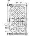
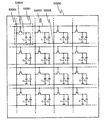
図28に、図9や図47に適用できる場合の上面図を示す。図28は、1画素分(1色要素分)を示している。半導体層2803aが形成され、その上に、ゲート配線2808a、容量線2808bが形成されている。ゲート配線2808aと一続きの膜であって、半導体層2803aの上に形成されたゲート電極によって、トランジスタが構成される。容量線2808bの下には、半導体層2803aが配置されており、容量線2808bと半導体層2803aとで、保持容量を形成している。ゲート絶縁膜を介して、上下の電極で容量を形成する。その場合、容量の電極となる領域の半導体層2803aは、リンやボロンが添付されていてもよいし、添付されていなくてもよい。添付されていない場合は、容量線2808bには、高い電圧が供給されている。リンやボロンが添付されている場合は、容量線2808bは、対向電極と電気的に接続されている場合が多い。これにより、配線数を減らすことが出来る。
FIG. 28 shows a top view of the case applicable to FIG. 9 and FIG. FIG. 28 shows one pixel (one color element). A
その上には、ソース信号線2809aやドレイン電極2809bが形成されている。それらは、コンタクトホールを介して、半導体層2803aと接続されている。
A
なお、ドレイン電極2809bを大きく配置し、容量線2808bと重なる領域を大きくとり、保持容量の容量値を大きくできるようにしてもよい。
Note that the
その上に、透明電極2806が形成されており、コンタクトホールを介して、ドレイン電極2809bと接続されている。その上には、反射電極2803bが形成されている。
A
反射電極2803bは、トランジスタや保持容量の上に形成されている。これにより、透過部での開口率を向上させることが出来、効率的にレイアウトすることができる。
The
なお、容量線2808bを配置しているが、これに限定されない。容量線2808bのかわりに、1行前のゲート信号線を用いても良い。つまり、1行前のゲート信号線は、非選択状態の時には、電位が一定であるので、保持容量線として機能させることが出来る。
Note that although the
なお、図28では、保持容量をトランジスタの近辺に配置したが、図29では、画素電極の中央部分に配置した。これにより、1画素の中に、透過部を複数設けることが出来る。したがって、液晶分子の配向状態が異なる領域が複数存在させることができ、マルチドメイン構造にしやすくすることが出来る。マルチドメイン構造にすると、視野角を広くすることが出来る。 In FIG. 28, the storage capacitor is disposed in the vicinity of the transistor, but in FIG. 29, the storage capacitor is disposed in the center portion of the pixel electrode. Thereby, a plurality of transmission parts can be provided in one pixel. Therefore, a plurality of regions having different alignment states of liquid crystal molecules can exist, and a multi-domain structure can be easily formed. A multi-domain structure can widen the viewing angle.
図30には、図27の場合に対して、反射電極に凹凸3001を形成した場合を示す。これは、図10や図13などに対応している。反射電極に凹凸を形成することにより、光が拡散され、輝度を上げることが出来る。
FIG. 30 shows a case where
同様に、図29の場合のように、保持容量を画素電極の中央部分に配置した場合に対して、反射電極に凹凸3001を形成した場合を図31に示す。反射電極に凹凸を形成することにより、光が拡散され、輝度を上げることが出来る。また、1画素の中に、透過部を複数設けることが出来るので、液晶分子の配向状態が異なる領域が複数存在させることができ、マルチドメイン構造にしやすくすることが出来る。マルチドメイン構造にすると、特定の角度で見たとき、光の透過量が減少してしまうことを防止することができ、視野角を広くすることが出来る。
Similarly, as shown in FIG. 29, FIG. 31 shows a case where the
次に、図11に示したように、凹部3201を形成した場合を図32に示す。これにより、セルギャップを反射部と透過部とで異なるようにすることができるため、視認性が向上し、正しい階調で、色むらの低減された画像を表示させることが出来る。また、セルギャップの調整を、トランジスタや容量や配線などが配置された側の基板で、同時に実現できるため、工程数が少なく、低コストで実現することが出来る。
Next, as shown in FIG. 11, the case where the
同様に、図29の場合のように、保持容量を画素電極の中央部分に配置した場合に対して、凹部3201a、3201bを形成した場合を図33に示す。
Similarly, FIG. 33 shows a case where the
図28〜図33では、画素電極が1画素ごとに、一面に配置されている場合を述べた。これは、主に、TN型液晶の時に用いる場合に相当する。 In FIG. 28 to FIG. 33, the case where the pixel electrodes are arranged on one surface for each pixel has been described. This corresponds mainly to the case of using the TN type liquid crystal.
しかし、図18、図19などに示したように、画素電極にスリットを入れることも可能であるし、画素電極を分割して間隔をおいて配置することも可能である。 However, as shown in FIGS. 18 and 19, the pixel electrode can be slit, or the pixel electrode can be divided and arranged at intervals.
図34では、画素電極にスリットを入れる又は画素電極を分割して間隔をおいて配置することにより、MVA型やPVA型などに対応させた場合の上面図を示す。透過領域においても、反射領域においても、スリット3401a、3401b、3401c、3401dなどを形成する。これにより、液晶分子の傾く方向を決めることが出来る。
FIG. 34 shows a top view in the case where the pixel electrode is made to correspond to the MVA type, the PVA type, or the like by slitting the pixel electrode or by dividing the pixel electrode and arranging them at intervals.
また、保持容量部を反射部の下に配置することにより、透過部の開口率を向上させることができ、最適なレイアウトを行うことが出来る。 In addition, by arranging the storage capacitor portion below the reflection portion, the aperture ratio of the transmission portion can be improved, and an optimal layout can be performed.
また、反射部や保持容量を画素電極の中央部に配置し、その上下に透過部を配置することにより、1画素の中に、透過部を複数設けることが出来るので、液晶分子の配向状態が異なる領域が複数存在させることができ、マルチドメイン構造にしやすくすることが出来る。これにより、特定の角度で見たとき、光の透過量が減少してしまうことを防止することができ、視野角を向上させることが出来る。 In addition, by arranging a reflective part and a storage capacitor in the center of the pixel electrode and arranging a transmissive part above and below the pixel electrode, a plurality of transmissive parts can be provided in one pixel. A plurality of different regions can exist, which can facilitate a multi-domain structure. Thereby, when it sees at a specific angle, it can prevent that the transmitted amount of light reduces, and can improve a viewing angle.
なお、反射部において、凹凸3001を形成した場合を図35に示す。反射電極に凹凸を形成することにより、光が拡散され、輝度を上げることが出来る。
Note that FIG. 35 shows a case where
このように、画素電極にスリットを入れる又は画素電極を分割して間隔をおいて配置する構成にするのは、図28〜図33にも適用させることが出来る。 In this manner, the configuration in which a slit is formed in the pixel electrode or the pixel electrode is divided and arranged at intervals can be applied to FIGS. 28 to 33.
なお、スリットの入れ方は、図34,図35に限定されず、様々な配置をすることが出来る。 In addition, how to insert a slit is not limited to FIG.34, FIG.35, Various arrangement | positioning can be performed.
図28〜図35において、トップゲート構造のトランジスタを用いた場合の一例を示した。ただし、これに限定されず、これら以外の構成も可能である。次に、逆スタガ構造のトランジスタを用いた場合の一例を示す。 In FIGS. 28 to 35, an example in the case of using a top-gate transistor is shown. However, the present invention is not limited to this, and other configurations are possible. Next, an example in which a transistor having an inverted stagger structure is used will be described.
図36は、図21に対応している。ゲート配線3608a、容量線3608bが形成されている。その上に、半導体層3603が形成される。ゲート配線3608aと一続きの膜であって、半導体層3603の下に形成されたゲート電極によって、トランジスタが構成される。その上には、ソース信号線3609aやドレイン電極3619bが形成されている。容量線3608bの上には、ドレイン電極3619bが配置されており、そこで、保持容量を形成している。ゲート絶縁膜を介して、上下の電極で容量を形成する。その上に、透明電極3606が形成されており、コンタクトホールを介して、ドレイン電極3619bと接続されている。その上には、反射電極3605が形成されている。
FIG. 36 corresponds to FIG. A
反射電極3605は、トランジスタや保持容量の上に形成されている。これにより、透過部での開口率を向上させることが出来、効率的にレイアウトすることができる。
The
図36では、保持容量をトランジスタの近辺に配置したが、画素電極の中央部分に配置してもよい。これにより、1画素の中に、透過部を複数設けることが出来るので、液晶分子の配向状態が異なる領域が複数存在させることができ、マルチドメイン構造にしやすくすることが出来る。マルチドメイン構造にすると、特定の角度で見たとき、光の透過量が減少してしまうことを防止することができ、視野角を広くすることが出来る。 In FIG. 36, the storage capacitor is disposed in the vicinity of the transistor, but may be disposed in the center portion of the pixel electrode. Accordingly, since a plurality of transmission portions can be provided in one pixel, a plurality of regions having different alignment states of liquid crystal molecules can exist, and a multi-domain structure can be easily formed. When the multi-domain structure is used, it is possible to prevent the amount of transmitted light from decreasing when viewed from a specific angle, and to widen the viewing angle.
図37には、図36の場合に対して、反射電極に凹凸3701を形成した場合を示す。これは、図22や図25などに対応している。反射電極に凹凸を形成することにより、光が拡散され、輝度を上げることが出来る。
FIG. 37 shows a case where
次に、図23に示したように、凹部3801を形成した場合を図38に示す。これにより、セルギャップを反射部と透過部とで異なるようにすることができるため、視認性が向上し、正しい階調で、色むらの低減された画像を表示させることが出来る。
Next, as shown in FIG. 23, the case where the
図36〜図38では、画素電極が1画素ごとに、一面に配置されている場合を述べた。これは、主に、TN型液晶の時に用いる場合に相当する。 In FIGS. 36 to 38, the case where the pixel electrodes are arranged on one surface for each pixel has been described. This corresponds mainly to the case of using the TN type liquid crystal.
しかし、図18、図19などに示したように、画素電極にスリットを入れることも可能であるし、画素電極を分割して間隔をおいて配置することも可能である。 However, as shown in FIGS. 18 and 19, the pixel electrode can be slit, or the pixel electrode can be divided and arranged at intervals.
図39では、画素電極にスリットを入れる又は画素電極を分割して間隔をおいて配置することにより、MVA型やPVA型などに対応させた場合の上面図を示す。透過領域においても、反射領域においても、スリット3901a、3901b、3901c、3901dなどを形成する。これにより、液晶分子の傾く方向を決めることが出来る。
FIG. 39 shows a top view when the pixel electrode is made to correspond to the MVA type, the PVA type, or the like by putting a slit in the pixel electrode or by dividing the pixel electrode and arranging them at intervals.
また、保持容量部を反射部の下に配置することにより、透過部の開口率を向上させることができ、最適なレイアウトを行うことが出来る。 In addition, by arranging the storage capacitor portion below the reflection portion, the aperture ratio of the transmission portion can be improved, and an optimal layout can be performed.
また、反射部や保持容量を画素電極の中央部に配置し、その上下に透過部を配置することにより、マルチドメイン構造にしやすくすることが出来る。これにより、特定の角度で見たとき、光の透過量が減少してしまうことを防止することができ、視野角を向上させることが出来る。 In addition, the multi-domain structure can be facilitated by disposing the reflective portion and the storage capacitor at the center of the pixel electrode and disposing the transmissive portions above and below the reflective portion. Thereby, when it sees at a specific angle, it can prevent that the transmitted amount of light reduces, and can improve a viewing angle.
なお、反射部(反射電極3605aの上)において、凹凸を形成してもよい。
Note that unevenness may be formed in the reflective portion (on the
なお、図39でのスリットは波打つような形状をしている。これにより、液晶分子をより制御しやすくしている。 Note that the slit in FIG. 39 has a waved shape. This makes it easier to control the liquid crystal molecules.
このように、画素電極にスリットを入れる又は画素電極を分割して間隔をおいて配置する構成にするのは、他の上面図にも適用させることが出来る。 In this manner, the structure in which the pixel electrode is slit or the pixel electrode is divided and arranged at intervals can be applied to other top views.
なお、スリットの入れ方は、図39に限定されず、様々な配置をすることが出来る。 Note that the way of inserting the slit is not limited to FIG. 39, and various arrangements can be made.
なお、本実施の形態は、実施の形態1〜5で述べた内容を、より具体的に実現し、ある部分をより詳細に説明した場合の一例を示している。したがって、実施の形態1〜5で述べた内容は、本実施の形態にも適用することができるし、本実施の形態と組み合わせたりすることも出来る。
In addition, this Embodiment has shown an example when the content described in Embodiment 1-5 is implement | achieved more concretely and a certain part is demonstrated in detail. Therefore, the description in
また、本実施の形態の中において、さまざまな図を用いて述べてきたが、1つの図は、様々な構成要件により成り立っている。したがって、各々の図の中から、各々の構成要件に関して、組み合わせて、さらなる構成を作ることも可能である。 Further, in the present embodiment, description has been made using various drawings, but one drawing is constituted by various components. Therefore, it is also possible to combine the components in the respective drawings to make further configurations.
(実施の形態7)
本実施の形態では、実施の形態1〜6で用いた露光マスクについて図20を用いて説明する。図20(A)〜(C)は、図1、図3、図7、図8で示した露光マスクの遮光部101a及び半透部101bの上面図を示す。露光マスクの遮光部101aの幅はt1と示し、半透部101bの幅はt2と示している。
(Embodiment 7)
In this embodiment, the exposure mask used in
半透部101bには回折格子パターンを設けることができ、図20(A)、(B)には露光装置の解像限界以下の複数のスリットでなるスリット部を有する回折格子パターンが示されている。回折格子パターンとは、スリット、ドット等のパターンが少なくとも1つ以上配置されたパターンである。スリット、ドット等のパターンを複数配置する場合は、周期的に配置されていてもよいし、非周期的に配置されてもよい。解像度限界以下の微細パターンを用いることによって、実質的な露光量を変調することが可能であり、露光されたレジストの現像後の膜厚を調節することが可能である。 A diffraction grating pattern can be provided in the semi-transmissive portion 101b, and FIGS. 20A and 20B show a diffraction grating pattern having a slit portion composed of a plurality of slits that are below the resolution limit of the exposure apparatus. Yes. The diffraction grating pattern is a pattern in which at least one pattern such as a slit and a dot is arranged. When a plurality of patterns such as slits and dots are arranged, they may be arranged periodically or aperiodically. By using a fine pattern below the resolution limit, it is possible to modulate the substantial exposure amount and to adjust the film thickness after development of the exposed resist.
該スリット部のスリットが延びる方向は、スリット部301の様に遮光部303の一辺と平行でも、スリット部302の様に遮光部303の一辺と垂直でも構わない。または、遮光部303の一辺に対して斜めの方向がスリットの延びる方向でも良い。尚、このフォトリソグラフィ工程で使用されるレジストはポジ型レジストが好ましい。
The direction in which the slit of the slit portion extends may be parallel to one side of the
また、半透部の別の例として、図20(C)に、露光光の光強度を低減する機能を有する半透膜2004を設けた例を示す。半透膜としては、MoSiNの他に、MoSi、MoSiO、MoSiON、CrSiなどを用いることができる。半透部を備えた露光マスクを用いた露光法は、ハーフトーン露光法とも呼ばれる。
As another example of the semi-transmissive portion, FIG. 20C illustrates an example in which a
これら図20(A)〜(C)に示す露光マスクに露光光を照射した場合、遮光部303の光強度はゼロであり、透光部305の光強度は100%である。一方、スリット部301、302、または半透膜2004で構成される光強度低減機能を有する半透部を通過する光の強度は、10〜70%の範囲で調整可能となっている。代表的な光強度分布の例を図20(D)に示す。半透部が回折格子パターンである場合には、半透部を通過する光強度の調整は、スリット部301、302のピッチ及びスリット幅の調整により実現している。
When the exposure mask shown in FIGS. 20A to 20C is irradiated with exposure light, the light intensity of the
また、本実施の形態は実施の形態1〜6と自由に組み合わせることができる。
Further, this embodiment can be freely combined with
(実施の形態8)
本発明の画素回路について述べる。図45に画素配列50000には、画素50001がマトリックス状に配置されている。画素50001には、ビデオ信号が入力されるソース信号線50002、ゲート信号が入力されるゲート信号線50003が接続されている。それらの信号を用いてトランジスタ50004を制御して、液晶CLC、保持容量Csにビデオ信号を入力する。保持容量Csは、保持容量線50005と接続されている。そして、ビデオ信号に応じて、液晶CLCの光透過率が変化し、画像を表示する。
(Embodiment 8)
The pixel circuit of the present invention will be described. In the
ガラス基板60000上には、図46に示すように、少なくとも画素配列50000が配置されている。そして、ゲート信号線を駆動するためのゲート信号線駆動回路60001や、ソース信号線にビデオ信号を供給するためのソース信号線駆動回路60002が配置されている場合がある。両方配置されている場合もあれば、いずれか一つのみ配置されていることもある。
On the
ソース信号線駆動回路60002には、シフトレジスタやサンプリングスイッチやラッチ回路やDAコンバータ回路などが配置されているが、これに限定されない。サンプリングスイッチのみ配置されて、シフトレジスタなどは配置されない場合もある。
The source signal
なお、本実施の形態は、実施の形態1〜7で述べた内容を、より具体的に実現し、ある部分をより詳細に説明した場合の一例を示している。したがって、実施の形態1〜7で述べた内容は、本実施の形態にも適用することができるし、本実施の形態と組み合わせることも出来る。
In addition, this Embodiment has shown an example when the content described in Embodiment 1-7 is implement | achieved more concretely and a certain part is demonstrated in detail. Therefore, the description in
また、本実施の形態の中において、さまざまな図を用いて述べてきたが、1つの図は、様々な構成要件により成り立っている。したがって、各々の図の中から、各々の構成要件に関して、組み合わせて、さらなる構成を作ることも可能である。 Further, in the present embodiment, description has been made using various drawings, but one drawing is constituted by various components. Therefore, it is also possible to combine the components in the respective drawings to make further configurations.
(実施の形態9)
本発明の表示装置を表示部に有する携帯電話の構成例について図40を用いて説明する。
(Embodiment 9)
A structural example of a cellular phone including the display device of the present invention in a display portion will be described with reference to FIG.
表示パネル5410はハウジング5400に脱着自在に組み込まれる。ハウジング5400は表示パネル5410のサイズに合わせて、形状や寸法を適宜変更することができる。表示パネル5410を固定したハウジング5400はプリント基板5401に嵌入されモジュールとして組み立てられる。 The display panel 5410 is incorporated in a housing 5400 so as to be detachable. The shape and dimensions of the housing 5400 can be changed as appropriate in accordance with the size of the display panel 5410. A housing 5400 to which the display panel 5410 is fixed is fitted into a printed board 5401 and assembled as a module.
表示パネル5410はFPC5411を介してプリント基板5401に接続される。プリント基板5401には、スピーカ5402、マイクロフォン5403、送受信回路5404、CPU及びコントローラなどを含む信号処理回路5405が形成されている。このようなモジュールと、入力手段5406、バッテリ5407を組み合わせ、筐体5409、5412に収納する。表示パネル5410の画素部は筐体5412に形成された開口窓から視認できように配置する。
The display panel 5410 is connected to the printed board 5401 through the
表示パネル5410は、画素部と一部の周辺駆動回路(複数の駆動回路のうち動作周波数の低い駆動回路)を基板上にTFTを用いて一体形成し、一部の周辺駆動回路(複数の駆動回路のうち動作周波数の高い駆動回路)をICチップ上に形成し、そのICチップをCOG(Chip On Glass)で表示パネル5410に実装しても良い。あるいは、そのICチップをTAB(Tape Auto Bonding)やプリント基板を用いてガラス基板と接続してもよい。なお、一部の周辺駆動回路を基板上に画素部と一体形成し、他の周辺駆動回路を形成したICチップをCOG等で実装した表示パネルの構成は図41(a)に一例を示してある。このような構成とすることで、表示装置の低消費電力を図り、携帯電話機の一回の充電による使用時間を長くすることができる。また、携帯電話機の低コスト化を図ることができる。 In the display panel 5410, a pixel portion and some peripheral driver circuits (a driver circuit having a low operating frequency among a plurality of driver circuits) are formed over a substrate using TFTs, and some peripheral driver circuits (a plurality of driver circuits) are formed. A driving circuit having a high operating frequency among the circuits) may be formed over the IC chip, and the IC chip may be mounted on the display panel 5410 by COG (Chip On Glass). Alternatively, the IC chip may be connected to the glass substrate using TAB (Tape Auto Bonding) or a printed board. Note that FIG. 41A shows an example of a configuration of a display panel in which some peripheral drive circuits are formed integrally with a pixel portion on a substrate and an IC chip on which other peripheral drive circuits are formed is mounted by COG or the like. is there. With such a structure, low power consumption of the display device can be achieved, and the use time by one charge of the mobile phone can be extended. In addition, the cost of the mobile phone can be reduced.
また、走査線や信号線に設定する信号をバッファによりインピーダンス変換することで、1行毎の画素の書き込み時間を短くすることができる。よって高精細な表示装置を提供することができる。 In addition, by performing impedance conversion of a signal set to the scanning line or the signal line using a buffer, the pixel writing time for each row can be shortened. Therefore, a high-definition display device can be provided.
さらに消費電力の低減を図るため、基板上にTFTを用いて画素部を形成し、全ての周辺駆動回路をICチップ上に形成し、そのICチップをCOG(Chip On Glass)などで表示パネルに実装しても良い。 In order to further reduce power consumption, a pixel portion is formed using TFTs on a substrate, all peripheral drive circuits are formed on an IC chip, and the IC chip is formed on a display panel by COG (Chip On Glass) or the like. May be implemented.
そして、本発明の表示装置を用いることにより、コントラストの高い画像で見ることが出来る。 Then, by using the display device of the present invention, an image with high contrast can be seen.
また、本実施例に示した構成は携帯電話の一例であって、本発明の表示装置はこのような構成の携帯電話に限られず様々な構成の携帯電話に適用することができる。 Further, the configuration shown in this embodiment is an example of a mobile phone, and the display device of the present invention is not limited to the mobile phone having such a configuration, and can be applied to mobile phones having various configurations.
なお、本実施の形態で述べた内容は、実施の形態1〜8で述べた内容と自由に組み合わせて実施することができる。
Note that the contents described in this embodiment can be implemented by being freely combined with the contents described in
また、本実施の形態の中において、さまざまな図を用いて述べてきたが、1つの図は、様々な構成要件により成り立っている。したがって、各々の図の中から、各々の構成要件に関して、組み合わせて、さらなる構成を作ることも可能である。 Further, in the present embodiment, description has been made using various drawings, but one drawing is constituted by various components. Therefore, it is also possible to combine the components in the respective drawings to make further configurations.
(実施の形態10)
図42は表示パネル5701と、回路基板5702を組み合わせた液晶モジュールを示している。表示パネル5701は画素部5703、走査線駆動回路5704及び信号線駆動回路5705を有している。回路基板5702には、例えば、コントロール回路5706や信号分割回路5707などが形成されている。表示パネル5701と回路基板5702は接続配線5708によって接続されている。接続配線にはFPC等を用いることができる。
(Embodiment 10)
FIG. 42 shows a liquid crystal module in which a
表示パネル5701は、画素部と一部の周辺駆動回路(複数の駆動回路のうち動作周波数の低い駆動回路)を基板上にTFTを用いて一体形成し、一部の周辺駆動回路(複数の駆動回路のうち動作周波数の高い駆動回路)をICチップ上に形成し、そのICチップをCOG(Chip On Glass)などで表示パネル5701に実装するとよい。あるいは、そのICチップをTAB(Tape Auto Bonding)やプリント基板を用いて表示パネル5701に実装しても良い。なお、一部の周辺駆動回路を基板上に画素部と一体形成し、他の周辺駆動回路を形成したICチップをCOG等で実装した構成は図41(a)に一例を示してある。このような構成とすることで、表示装置の低消費電力を図り、携帯電話機の一回の充電による使用時間を長くすることができる。また、携帯電話機の低コスト化を図ることができる。
In the
走査線や信号線に設定する信号をバッファによりインピーダンス変換することで、1行毎の画素の書き込み時間を短くすることができる。よって高精細な表示装置を提供することができる。 By performing impedance conversion of a signal set to the scanning line or the signal line using a buffer, the pixel writing time for each row can be shortened. Therefore, a high-definition display device can be provided.
さらに消費電力の低減を図るため、ガラス基板上にTFTを用いて画素部を形成し、全ての信号線駆動回路をICチップ上に形成し、そのICチップをCOG(Chip On Glass)表示パネルに実装してもよい。 In order to further reduce power consumption, a pixel portion is formed using a TFT on a glass substrate, all signal line driver circuits are formed on an IC chip, and the IC chip is formed on a COG (Chip On Glass) display panel. May be implemented.
なお、基板上にTFTを用いて画素部を形成し、全ての周辺駆動回路をICチップ上に形成し、そのICチップをCOG(Chip On Glass)で表示パネルに実装するとよい。なお、基板上に画素部を形成し、その基板上に信号線駆動回路を形成したICチップをCOG等で実装した構成は図41(b)に一例を示してある。 Note that a pixel portion is formed using a TFT over a substrate, all peripheral driver circuits are formed over an IC chip, and the IC chip is mounted on a display panel by COG (Chip On Glass). FIG. 41B shows an example of a structure in which an IC chip in which a pixel portion is formed over a substrate and a signal line driver circuit is formed over the substrate is mounted by COG or the like.
この液晶モジュールにより液晶テレビ受像機を完成させることができる。図43は、液晶テレビ受像機の主要な構成を示すブロック図である。チューナ5801は映像信号と音声信号を受信する。映像信号は、映像信号増幅回路5802と、そこから出力される信号を赤、緑、青の各色に対応した色信号に変換する映像信号処理回路5803と、その映像信号を駆動回路の入力仕様に変換するためのコントロール回路5706により処理される。コントロール回路5706は、走査線側と信号線側にそれぞれ信号が出力する。デジタル駆動する場合には、信号線側に信号分割回路5707を設け、入力デジタル信号をm個に分割して供給する構成としても良い。
With this liquid crystal module, a liquid crystal television receiver can be completed. FIG. 43 is a block diagram showing a main configuration of the liquid crystal television receiver. A
チューナ5801で受信した信号のうち、音声信号は音声信号増幅回路5804に送られ、その出力は音声信号処理回路5805を経てスピーカ5806に供給される。制御回路5807は受信局(受信周波数)や音量の制御情報を入力部5808から受け、チューナ5801や音声信号処理回路5805に信号を送出する。
Of the signals received by the
液晶モジュールを筐体に組みこんで、テレビ受像機を完成させることができる。液晶モジュールにより、表示部が形成される。また、スピーカ、ビデオ入力端子などが適宜備えられている。 A television receiver can be completed by incorporating a liquid crystal module into a housing. A display unit is formed by the liquid crystal module. In addition, a speaker, a video input terminal, and the like are provided as appropriate.
勿論、本発明はテレビ受像機に限定されず、パーソナルコンピュータのモニタをはじめ、鉄道の駅や空港などにおける情報表示盤や、街頭における広告表示盤など特に大面積の表示媒体として様々な用途に適用することができる。 Of course, the present invention is not limited to a television receiver, and is applied to various uses as a display medium of a particularly large area such as a monitor of a personal computer, an information display board in a railway station or airport, an advertisement display board in a street, etc. can do.
このように、本発明の表示装置を用いることにより、コントラストの高い画像で見ることが出来る。 Thus, by using the display device of the present invention, an image with high contrast can be seen.
なお、本実施の形態で述べた内容は、実施の形態1〜9で述べた内容と自由に組み合わせて実施することができる。
Note that the contents described in this embodiment can be implemented by being freely combined with the contents described in
また、本実施の形態の中において、さまざまな図を用いて述べてきたが、1つの図は、様々な構成要件により成り立っている。したがって、各々の図の中から、各々の構成要件に関して、組み合わせて、さらなる構成を作ることも可能である。 Further, in the present embodiment, description has been made using various drawings, but one drawing is constituted by various components. Therefore, it is also possible to combine the components in the respective drawings to make further configurations.
(実施の形態11)
本発明は様々な電子機器に適用することができる。具体的には電子機器の表示部に適用することができる。そのような電子機器として、ビデオカメラ、デジタルカメラ、ゴーグル型ディスプレイ、ナビゲーションシステム、音響再生装置(カーオーディオ、オーディオコンポ等)、コンピュータ、ゲーム機器、携帯情報端末(モバイルコンピュータ、携帯電話、携帯型ゲーム機又は電子書籍等)、記録媒体を備えた画像再生装置(具体的にはDigital Versatile Disc(DVD)等の記録媒体を再生し、その画像を表示しうる表示装置を備えた装置)などが挙げられる。
(Embodiment 11)
The present invention can be applied to various electronic devices. Specifically, it can be applied to a display portion of an electronic device. Such electronic devices include video cameras, digital cameras, goggles-type displays, navigation systems, sound playback devices (car audio, audio components, etc.), computers, game devices, portable information terminals (mobile computers, mobile phones, portable games) Or an image reproducing apparatus (specifically, an apparatus having a display device capable of reproducing a recording medium such as Digital Versatile Disc (DVD) and displaying the image). It is done.
図44(A)は表示装置であり、筐体35001、支持台35002、表示部35003、スピーカ部35004、ビデオ入力端子35005等を含む。本発明の表示装置を表示部35003に用いることができる。なお、表示装置は、パーソナルコンピュータ用、テレビジョン放送受信用、広告表示用などの全ての情報表示用表示装置が含まれる。本発明の表示装置を表示部35003に用いた表示装置は、コントラストの高い画像で見ることが可能となる。
FIG. 44A illustrates a display device, which includes a
図44(B)はカメラであり、本体35101、表示部35102、受像部35103、操作キー35104、外部接続ポート35105、シャッター35106等を含む。
FIG. 44B shows a camera, which includes a
本発明を表示部35102に用いたデジタルカメラは、コントラストの高い画像で見ることが可能となる。
A digital camera using the present invention for the
図44(C)はコンピュータであり、本体35201、筐体35202、表示部35203、キーボード35204、外部接続ポート35205、ポインティングデバイス35206等を含む。本発明を表示部35203に用いたコンピュータは、コントラストの高い画像で見ることが可能となる。
FIG. 44C illustrates a computer, which includes a
図44(D)はモバイルコンピュータであり、本体35301、表示部35302、スイッチ35303、操作キー35304、赤外線ポート35305等を含む。本発明を表示部35302に用いたモバイルコンピュータは、コントラストの高い画像で見ることが可能となる。
FIG. 44D shows a mobile computer, which includes a
図44(E)は記録媒体を備えた携帯型の画像再生装置(具体的にはDVD再生装置)であり、本体35401、筐体35402、表示部A35403、表示部B35404、記録媒体(DVD等)読み込み部35405、操作キー35406、スピーカ部35407等を含む。表示部A35403は主として画像情報を表示し、表示部B35404は主として文字情報を表示することができる。本発明を表示部A35403や表示部B35404に用いた画像再生装置は、コントラストの高い画像で見ることが可能となる。
FIG. 44E shows a portable image reproducing device (specifically, a DVD reproducing device) provided with a recording medium, which includes a
図44(F)はゴーグル型ディスプレイであり、本体35501、表示部35502、アーム部35503を含む。本発明を表示部35502に用いたゴーグル型ディスプレイは、コントラストの高い画像で見ることが可能となる。
FIG. 44F illustrates a goggle type display which includes a
図44(G)はビデオカメラであり、本体35601、表示部35602、筐体35603、外部接続ポート35604、リモコン受信部35605、受像部35606、バッテリ35607、音声入力部35608、操作キー35609、接眼部35610等を含む。本発明を表示部35602に用いたビデオカメラは、コントラストの高い画像で見ることが可能となる。
FIG. 44G illustrates a video camera, which includes a main body 35601, a
図44(H)は携帯電話機であり、本体35701、筐体35702、表示部35703、音声入力部35704、音声出力部35705、操作キー35706、外部接続ポート35707、アンテナ35708等を含む。本発明を表示部35703に用いた携帯電話機は、コントラストの高い画像で見ることが可能となる。
FIG. 44H shows a cellular phone, which includes a
以上の様に、本発明の適用範囲は極めて広く、あらゆる分野の電子機器に用いることが可能である。また本実施の形態の電子機器は、実施の形態1〜13に示したいずれの構成の表示装置を用いても良い。
As described above, the applicable range of the present invention is so wide that it can be used for electronic devices in various fields. In addition, the electronic device of this embodiment may use the display device having any structure described in
Claims (9)
前記トランジスタに電気的に接続する透明電極と、
前記透明電極に電気的に接続する反射電極と
前記トランジスタに電気的に接続する保持容量と、を有し、
前記反射電極の下に、前記保持容量の少なくとも一部が形成され、
前記反射電極の下面全体が前記透明電極の上面に接していることを特徴とする表示装置。 A transistor,
A transparent electrode electrically connected to the transistor;
A reflective electrode electrically connected to the transparent electrode and a storage capacitor electrically connected to the transistor,
Under the reflective electrode, at least a part of the storage capacitor is formed,
The display device, wherein the entire lower surface of the reflective electrode is in contact with the upper surface of the transparent electrode.
前記トランジスタに電気的に接続する透明電極と、
前記透明電極に電気的に接続する反射電極と、を有し、
前記透明電極もしくは前記反射電極の少なくとも1つは、スリットを有し、
前記反射電極の下面全体が前記透明電極の上面に接していることを特徴とする表示装置。 A transistor,
A transparent electrode electrically connected to the transistor;
A reflective electrode electrically connected to the transparent electrode,
At least one of the transparent electrode or the reflective electrode has a slit,
The display device, wherein the entire lower surface of the reflective electrode is in contact with the upper surface of the transparent electrode.
前記トランジスタに電気的に接続する透明電極と、
前記透明電極に電気的に接続する反射電極と、
前記トランジスタに電気的に接続する保持容量と、を有し、
前記透明電極もしくは前記反射電極の少なくとも1つは、スリットを有し、
前記反射電極の下に、前記保持容量の少なくとも一部が形成され、
前記反射電極の下面全体が前記透明電極の上面に接していることを特徴とする表示装置。 A transistor,
A transparent electrode electrically connected to the transistor;
A reflective electrode electrically connected to the transparent electrode;
A storage capacitor electrically connected to the transistor,
At least one of the transparent electrode or the reflective electrode has a slit,
Under the reflective electrode, at least a part of the storage capacitor is formed,
The display device, wherein the entire lower surface of the reflective electrode is in contact with the upper surface of the transparent electrode.
前記トランジスタに電気的に接続する透明電極と、
前記透明電極に電気的に接続する反射電極と
前記トランジスタに電気的に接続する保持容量と、を有し、
前記反射電極の下に、前記保持容量の少なくとも一部が形成され、
前記反射電極の下に、前記トランジスタの少なくとも一部が形成され、
前記反射電極の下面全体が前記透明電極の上面に接していることを特徴とする表示装置。 A transistor,
A transparent electrode electrically connected to the transistor;
A reflective electrode electrically connected to the transparent electrode and a storage capacitor electrically connected to the transistor,
Under the reflective electrode, at least a part of the storage capacitor is formed,
Under the reflective electrode, at least a part of the transistor is formed,
The display device, wherein the entire lower surface of the reflective electrode is in contact with the upper surface of the transparent electrode.
前記トランジスタに電気的に接続する画素電極と、を有し、
前記画素電極は、透明電極と反射電極とを有し、
前記反射電極の下面全体が前記透明電極の上面に接しており、
前記反射電極と接する領域での前記透明電極の膜厚は、前記反射電極と接しない領域での前記透明電極の膜厚よりも厚いことを特徴とする表示装置。 A transistor,
A pixel electrode electrically connected to the transistor,
The pixel electrode has a transparent electrode and a reflective electrode,
The entire lower surface of the reflective electrode is in contact with the upper surface of the transparent electrode;
The display device, wherein a film thickness of the transparent electrode in a region in contact with the reflective electrode is larger than a film thickness of the transparent electrode in a region not in contact with the reflective electrode.
前記反射電極と、対向電極との間に液晶層が配置されていることを特徴とする表示装置。 In any one of Claims 1 thru | or 5,
A display device, wherein a liquid crystal layer is disposed between the reflective electrode and the counter electrode.
前記トランジスタの上に絶縁膜を形成し、
前記絶縁膜の上に透明導電膜を形成し、
前記透明導電膜の上に反射導電膜を形成し、
前記反射導電膜の上に半透部を有する露光マスクを用いて、膜厚の厚い領域と該領域よりも膜厚の薄い領域とを有するレジストパターンを形成し、
前記レジストパターンを用いて、前記透明導電膜でなる透明電極と、前記反射導電膜でなる反射電極とを形成することを特徴とする表示装置の作製方法。 Forming transistors on the substrate,
Forming an insulating film on the transistor;
Forming a transparent conductive film on the insulating film;
Forming a reflective conductive film on the transparent conductive film;
Using an exposure mask having a semi-transmissive portion on the reflective conductive film, a resist pattern having a thick region and a thin region is formed.
A method for manufacturing a display device, wherein a transparent electrode made of the transparent conductive film and a reflective electrode made of the reflective conductive film are formed using the resist pattern.
前記トランジスタの上に絶縁膜を形成し、
前記絶縁膜の上に透明導電膜を形成し、
前記透明導電膜の上に反射導電膜を形成し、
前記反射導電膜の上に半透部を有する露光マスクを用いて、膜厚の厚い領域と該領域よりも膜厚の薄い領域とを有するレジストパターンを形成し、
前記レジストパターンを用いて、前記反射導電膜と前記透明導電膜とをエッチングし、
前記レジストパターンの一部を除去し、
前記一部が除去されたレジストパターンを用いて、前記反射導電膜をエッチングすることを特徴とする表示装置の作製方法。 Forming transistors on the substrate,
Forming an insulating film on the transistor;
Forming a transparent conductive film on the insulating film;
Forming a reflective conductive film on the transparent conductive film;
Using an exposure mask having a semi-transmissive portion on the reflective conductive film, a resist pattern having a thick region and a thin region is formed.
Using the resist pattern, etching the reflective conductive film and the transparent conductive film,
Removing a part of the resist pattern;
A method for manufacturing a display device, wherein the reflective conductive film is etched using a resist pattern from which the part has been removed.
Priority Applications (1)
| Application Number | Priority Date | Filing Date | Title |
|---|---|---|---|
| JP2006351955A JP2007199708A (en) | 2005-12-28 | 2006-12-27 | Display device and manufacturing method thereof |
Applications Claiming Priority (2)
| Application Number | Priority Date | Filing Date | Title |
|---|---|---|---|
| JP2005378778 | 2005-12-28 | ||
| JP2006351955A JP2007199708A (en) | 2005-12-28 | 2006-12-27 | Display device and manufacturing method thereof |
Related Child Applications (2)
| Application Number | Title | Priority Date | Filing Date |
|---|---|---|---|
| JP2010046764A Division JP5025743B2 (en) | 2005-12-28 | 2010-03-03 | Liquid crystal display device, display module, electronic equipment |
| JP2011241768A Division JP5063807B2 (en) | 2005-12-28 | 2011-11-03 | Display device, display module, electronic device |
Publications (2)
| Publication Number | Publication Date |
|---|---|
| JP2007199708A true JP2007199708A (en) | 2007-08-09 |
| JP2007199708A5 JP2007199708A5 (en) | 2009-12-03 |
Family
ID=38454333
Family Applications (1)
| Application Number | Title | Priority Date | Filing Date |
|---|---|---|---|
| JP2006351955A Withdrawn JP2007199708A (en) | 2005-12-28 | 2006-12-27 | Display device and manufacturing method thereof |
Country Status (1)
| Country | Link |
|---|---|
| JP (1) | JP2007199708A (en) |
Cited By (18)
| Publication number | Priority date | Publication date | Assignee | Title |
|---|---|---|---|---|
| JP2009008892A (en) * | 2007-06-28 | 2009-01-15 | Sumitomo Metal Mining Co Ltd | Transflective electrode substrate and method for manufacturing the same, and transflective liquid crystal display device with the transflective electrode substrate used therewith |
| JP2009251174A (en) * | 2008-04-03 | 2009-10-29 | Mitsubishi Electric Corp | Tft substrate, liquid crystal display device using the same, and method for manufacturing them |
| JP2010107570A (en) * | 2008-10-28 | 2010-05-13 | Kobe Steel Ltd | Method for manufacturing display device |
| JP2010262007A (en) * | 2009-04-30 | 2010-11-18 | Sony Corp | Display and method for manufacturing display |
| JP2011022232A (en) * | 2009-07-14 | 2011-02-03 | Sony Corp | Liquid crystal display device, method of manufacturing the same, and electronic device |
| JP2011186079A (en) * | 2010-03-05 | 2011-09-22 | Semiconductor Energy Lab Co Ltd | Liquid crystal display device |
| JP2012003256A (en) * | 2010-05-20 | 2012-01-05 | Semiconductor Energy Lab Co Ltd | Liquid crystal display device and manufacturing method of the same |
| KR20120031365A (en) * | 2010-09-24 | 2012-04-03 | 삼성모바일디스플레이주식회사 | Organic light emitting display device |
| JP2012137771A (en) * | 2006-11-14 | 2012-07-19 | Mitsubishi Electric Corp | Methods for manufacturing multilayer thin film pattern and display device |
| US9041202B2 (en) | 2008-05-16 | 2015-05-26 | Semiconductor Energy Laboratory Co., Ltd. | Semiconductor device and manufacturing method of the same |
| JP2015146053A (en) * | 2005-12-28 | 2015-08-13 | 株式会社半導体エネルギー研究所 | display device |
| US9257082B2 (en) | 2009-09-04 | 2016-02-09 | Semiconductor Energy Laboratory Co., Ltd. | Display device and electronic device |
| JP2018032021A (en) * | 2016-08-17 | 2018-03-01 | 株式会社半導体エネルギー研究所 | Display device |
| JP2018513413A (en) * | 2015-06-24 | 2018-05-24 | 深▲せん▼市華星光電技術有限公司Shenzhen China Star Optoelectronics Technology Co., Ltd. | Thin film transistor array substrate and manufacturing method thereof |
| JP2019074684A (en) * | 2017-10-18 | 2019-05-16 | シャープ株式会社 | Method for manufacturing substrate for display panel |
| JP2020129132A (en) * | 2020-04-28 | 2020-08-27 | 株式会社ジャパンディスプレイ | Semiconductor device |
| JP2020129113A (en) * | 2015-08-28 | 2020-08-27 | 群創光電股▲ふん▼有限公司Innolux Corporation | Display device |
| JP2021185423A (en) * | 2013-07-10 | 2021-12-09 | 株式会社半導体エネルギー研究所 | Display device |
Citations (5)
| Publication number | Priority date | Publication date | Assignee | Title |
|---|---|---|---|---|
| JP2002094064A (en) * | 2000-09-11 | 2002-03-29 | Matsushita Electric Ind Co Ltd | Thin-film transistor, method for manufacturing the same, liquid crystal display device and electroluminescence display device |
| JP2002134756A (en) * | 2000-10-26 | 2002-05-10 | Matsushita Electric Ind Co Ltd | Semiconductor device and manufacturing method therefor |
| JP2003207774A (en) * | 2001-10-30 | 2003-07-25 | Nec Corp | Semi-transmission type liquid crystal display and fabrication method thereof |
| JP2005258410A (en) * | 2004-03-08 | 2005-09-22 | Samsung Electronics Co Ltd | Liquid crystal display apparatus and method of manufacturing the same |
| JP2005275213A (en) * | 2004-03-26 | 2005-10-06 | Sharp Corp | Liquid crystal display device |
-
2006
- 2006-12-27 JP JP2006351955A patent/JP2007199708A/en not_active Withdrawn
Patent Citations (5)
| Publication number | Priority date | Publication date | Assignee | Title |
|---|---|---|---|---|
| JP2002094064A (en) * | 2000-09-11 | 2002-03-29 | Matsushita Electric Ind Co Ltd | Thin-film transistor, method for manufacturing the same, liquid crystal display device and electroluminescence display device |
| JP2002134756A (en) * | 2000-10-26 | 2002-05-10 | Matsushita Electric Ind Co Ltd | Semiconductor device and manufacturing method therefor |
| JP2003207774A (en) * | 2001-10-30 | 2003-07-25 | Nec Corp | Semi-transmission type liquid crystal display and fabrication method thereof |
| JP2005258410A (en) * | 2004-03-08 | 2005-09-22 | Samsung Electronics Co Ltd | Liquid crystal display apparatus and method of manufacturing the same |
| JP2005275213A (en) * | 2004-03-26 | 2005-10-06 | Sharp Corp | Liquid crystal display device |
Cited By (41)
| Publication number | Priority date | Publication date | Assignee | Title |
|---|---|---|---|---|
| US11269214B2 (en) | 2005-12-28 | 2022-03-08 | Semiconductor Energy Laboratory Co., Ltd. | Display device and manufacturing method thereof |
| US10739637B2 (en) | 2005-12-28 | 2020-08-11 | Semiconductor Energy Laboratory Co., Ltd. | Display device and manufacturing method thereof |
| US10444564B1 (en) | 2005-12-28 | 2019-10-15 | Semiconductor Energy Laboratory Co., Ltd. | Display device and manufacturing method thereof |
| US9703140B2 (en) | 2005-12-28 | 2017-07-11 | Semiconductor Energy Laboratory Co., Ltd. | Display device and manufacturing method thereof |
| JP2015146053A (en) * | 2005-12-28 | 2015-08-13 | 株式会社半導体エネルギー研究所 | display device |
| JP2012137771A (en) * | 2006-11-14 | 2012-07-19 | Mitsubishi Electric Corp | Methods for manufacturing multilayer thin film pattern and display device |
| JP2009008892A (en) * | 2007-06-28 | 2009-01-15 | Sumitomo Metal Mining Co Ltd | Transflective electrode substrate and method for manufacturing the same, and transflective liquid crystal display device with the transflective electrode substrate used therewith |
| JP2009251174A (en) * | 2008-04-03 | 2009-10-29 | Mitsubishi Electric Corp | Tft substrate, liquid crystal display device using the same, and method for manufacturing them |
| US11133332B2 (en) | 2008-05-16 | 2021-09-28 | Semiconductor Energy Laboratory Co., Ltd. | Semiconductor device and manufacturing method of the same |
| US9041202B2 (en) | 2008-05-16 | 2015-05-26 | Semiconductor Energy Laboratory Co., Ltd. | Semiconductor device and manufacturing method of the same |
| US11646322B2 (en) | 2008-05-16 | 2023-05-09 | Semiconductor Energy Laboratory Co., Ltd. | Semiconductor device having conductive oxide electrode layers in direct contact with oxide semiconductor layer |
| US10580797B2 (en) | 2008-05-16 | 2020-03-03 | Semiconductor Energy Laboratory Co., Ltd. | Semiconductor device and manufacturing method of the same |
| US9397255B2 (en) | 2008-05-16 | 2016-07-19 | Semiconductor Energy Laboratory Co., Ltd. | Semiconductor device and manufacturing method of the same |
| JP2010107570A (en) * | 2008-10-28 | 2010-05-13 | Kobe Steel Ltd | Method for manufacturing display device |
| JP2010262007A (en) * | 2009-04-30 | 2010-11-18 | Sony Corp | Display and method for manufacturing display |
| US8553194B2 (en) | 2009-07-14 | 2013-10-08 | Japan Display West Inc. | Liquid crystal display device, liquid crystal display device manufacturing method, and electronic device |
| JP2011022232A (en) * | 2009-07-14 | 2011-02-03 | Sony Corp | Liquid crystal display device, method of manufacturing the same, and electronic device |
| US11652174B2 (en) | 2009-09-04 | 2023-05-16 | Semiconductor Energy Laboratory Co., Ltd. | Display device and electronic device |
| US11430899B2 (en) | 2009-09-04 | 2022-08-30 | Semiconductor Energy Laboratory Co., Ltd. | Display device and electronic device |
| US10134912B2 (en) | 2009-09-04 | 2018-11-20 | Semiconductor Energy Laboratory Co., Ltd. | Display device and electronic device |
| US11069817B2 (en) | 2009-09-04 | 2021-07-20 | Semiconductor Energy Laboratory Co., Ltd. | Display device and electronic device |
| US11935965B2 (en) | 2009-09-04 | 2024-03-19 | Semiconductor Energy Laboratory Co., Ltd. | Display device and electronic device |
| US10700215B2 (en) | 2009-09-04 | 2020-06-30 | Semiconductor Energy Laboratory Co., Ltd. | Display device and electronic device |
| US9257082B2 (en) | 2009-09-04 | 2016-02-09 | Semiconductor Energy Laboratory Co., Ltd. | Display device and electronic device |
| JP2011186079A (en) * | 2010-03-05 | 2011-09-22 | Semiconductor Energy Lab Co Ltd | Liquid crystal display device |
| JP2012003256A (en) * | 2010-05-20 | 2012-01-05 | Semiconductor Energy Lab Co Ltd | Liquid crystal display device and manufacturing method of the same |
| JP2017146630A (en) * | 2010-05-20 | 2017-08-24 | 株式会社半導体エネルギー研究所 | Liquid crystal display device and method of manufacturing the same |
| US9337218B2 (en) | 2010-05-20 | 2016-05-10 | Semiconductor Energy Laboratory Co., Ltd. | Liquid crystal display device and manufacturing method thereof |
| KR101954981B1 (en) * | 2010-09-24 | 2019-03-08 | 삼성디스플레이 주식회사 | Organic light emitting display device |
| KR20120031365A (en) * | 2010-09-24 | 2012-04-03 | 삼성모바일디스플레이주식회사 | Organic light emitting display device |
| US11869453B2 (en) | 2013-07-10 | 2024-01-09 | Semiconductor Energy Laboratory Co., Ltd. | Display device comprising semiconductor layer having LDD regions |
| JP2021185423A (en) * | 2013-07-10 | 2021-12-09 | 株式会社半導体エネルギー研究所 | Display device |
| JP2018513413A (en) * | 2015-06-24 | 2018-05-24 | 深▲せん▼市華星光電技術有限公司Shenzhen China Star Optoelectronics Technology Co., Ltd. | Thin film transistor array substrate and manufacturing method thereof |
| US11686987B2 (en) | 2015-08-28 | 2023-06-27 | Innolux Corporation | Display device |
| JP2020129113A (en) * | 2015-08-28 | 2020-08-27 | 群創光電股▲ふん▼有限公司Innolux Corporation | Display device |
| JP2018032021A (en) * | 2016-08-17 | 2018-03-01 | 株式会社半導体エネルギー研究所 | Display device |
| JP7049784B2 (en) | 2016-08-17 | 2022-04-07 | 株式会社半導体エネルギー研究所 | Display device |
| US10620468B2 (en) | 2017-10-18 | 2020-04-14 | Sharp Kabushiki Kaisha | Method of manufacturing display panel substrate |
| JP2019074684A (en) * | 2017-10-18 | 2019-05-16 | シャープ株式会社 | Method for manufacturing substrate for display panel |
| JP7065147B2 (en) | 2020-04-28 | 2022-05-11 | 株式会社ジャパンディスプレイ | Semiconductor device |
| JP2020129132A (en) * | 2020-04-28 | 2020-08-27 | 株式会社ジャパンディスプレイ | Semiconductor device |
Similar Documents
| Publication | Publication Date | Title |
|---|---|---|
| JP6605050B2 (en) | Method for manufacturing display device | |
| JP2007199708A (en) | Display device and manufacturing method thereof | |
| JP6603425B2 (en) | Active matrix display device, mobile phone |
Legal Events
| Date | Code | Title | Description |
|---|---|---|---|
| A521 | Written amendment |
Free format text: JAPANESE INTERMEDIATE CODE: A523 Effective date: 20091016 |
|
| A621 | Written request for application examination |
Free format text: JAPANESE INTERMEDIATE CODE: A621 Effective date: 20091016 |
|
| A977 | Report on retrieval |
Free format text: JAPANESE INTERMEDIATE CODE: A971007 Effective date: 20111020 |
|
| A131 | Notification of reasons for refusal |
Free format text: JAPANESE INTERMEDIATE CODE: A131 Effective date: 20111025 |
|
| A521 | Written amendment |
Free format text: JAPANESE INTERMEDIATE CODE: A523 Effective date: 20111107 |
|
| A02 | Decision of refusal |
Free format text: JAPANESE INTERMEDIATE CODE: A02 Effective date: 20120417 |
|
| A761 | Written withdrawal of application |
Free format text: JAPANESE INTERMEDIATE CODE: A761 Effective date: 20120622 |