JP2007123718A - 電子回路装置 - Google Patents
電子回路装置 Download PDFInfo
- Publication number
- JP2007123718A JP2007123718A JP2005316770A JP2005316770A JP2007123718A JP 2007123718 A JP2007123718 A JP 2007123718A JP 2005316770 A JP2005316770 A JP 2005316770A JP 2005316770 A JP2005316770 A JP 2005316770A JP 2007123718 A JP2007123718 A JP 2007123718A
- Authority
- JP
- Japan
- Prior art keywords
- circuit device
- connection terminal
- electronic circuit
- circuit board
- hole
- Prior art date
- Legal status (The legal status is an assumption and is not a legal conclusion. Google has not performed a legal analysis and makes no representation as to the accuracy of the status listed.)
- Pending
Links
- 229910000679 solder Inorganic materials 0.000 claims abstract description 32
- 230000000149 penetrating effect Effects 0.000 claims abstract description 3
- 239000004020 conductor Substances 0.000 claims description 16
- 230000000694 effects Effects 0.000 description 4
- 238000012545 processing Methods 0.000 description 4
- 230000008602 contraction Effects 0.000 description 3
- 230000008878 coupling Effects 0.000 description 3
- 238000010168 coupling process Methods 0.000 description 3
- 238000005859 coupling reaction Methods 0.000 description 3
- 230000001105 regulatory effect Effects 0.000 description 3
- 238000005476 soldering Methods 0.000 description 3
- 239000003990 capacitor Substances 0.000 description 2
- 238000007796 conventional method Methods 0.000 description 1
- 238000006073 displacement reaction Methods 0.000 description 1
- 238000003780 insertion Methods 0.000 description 1
- 230000037431 insertion Effects 0.000 description 1
- 239000007769 metal material Substances 0.000 description 1
- 238000012986 modification Methods 0.000 description 1
- 230000004048 modification Effects 0.000 description 1
- 239000000758 substrate Substances 0.000 description 1
Images

Landscapes
- Multi-Conductor Connections (AREA)
- Coupling Device And Connection With Printed Circuit (AREA)
- Structures For Mounting Electric Components On Printed Circuit Boards (AREA)
Abstract
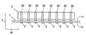
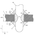
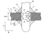
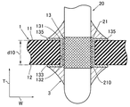
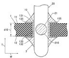
【解決手段】電子回路装置は、回路基板1と、電子部品2と、はんだ3とを含む。回路基板1は、一面11から他面12に貫通するスルーホール13を有する。スルーホール13の内面133には、導体膜135が備えられている。電子部品2は、接続端子20を有し、回路基板1の一面11に載置されている。接続端子20は、凹部21を有し、凹部21は、少なくともスルーホール13の内部に配置されている。はんだ3は、スルーホール13の内部において、導体膜135の表面と、凹部21の内面210との間に充填されており、回路基板1と、接続端子20とを固着している。
【選択図】図2
Description
(1)優れた結合強度を有し、信頼性を向上することができる電子回路装置を提供することができる。
(2)加工コストを低減し、優れた生産性を有する電子回路装置を提供することができる。
11 一面
12 他面
13 スルーホール
133 内面
135 導体膜
2 電子部品
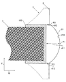
20 接続端子
21 凹部
220 内面
3 はんだ
Claims (4)
- 回路基板と、電子部品と、はんだとを含む電子回路装置であって、
前記回路基板は、一面から他面に貫通するスルーホールを有しており、
前記スルーホールは、内面に導体膜が備えられており、
前記電子部品は、接続端子を有し、前記回路基板の一面に載置されており、
前記接続端子は、凹部を有し、前記凹部は、前記スルーホールの内部に配置されており、
前記はんだは、前記スルーホールの内部において、少なくとも前記導体膜の表面と、前記凹部の内面との間に充填され、前記回路基板と、前記接続端子とを固着している、
電子回路装置。 - 請求項1に記載された電子回路装置であって、
前記凹部は、内面が弧状であり、両端部が前記スルーホールの開口端の付近に位置する、電子回路装置。 - 請求項1に記載された電子回路装置であって、
前記凹部は、ローレット加工により形成されている、電子回路装置。 - 請求項1に記載された電子回路装置であって、
前記凹部は、貫通孔である、電子回路装置。
Priority Applications (1)
| Application Number | Priority Date | Filing Date | Title |
|---|---|---|---|
| JP2005316770A JP2007123718A (ja) | 2005-10-31 | 2005-10-31 | 電子回路装置 |
Applications Claiming Priority (1)
| Application Number | Priority Date | Filing Date | Title |
|---|---|---|---|
| JP2005316770A JP2007123718A (ja) | 2005-10-31 | 2005-10-31 | 電子回路装置 |
Publications (1)
| Publication Number | Publication Date |
|---|---|
| JP2007123718A true JP2007123718A (ja) | 2007-05-17 |
Family
ID=38147204
Family Applications (1)
| Application Number | Title | Priority Date | Filing Date |
|---|---|---|---|
| JP2005316770A Pending JP2007123718A (ja) | 2005-10-31 | 2005-10-31 | 電子回路装置 |
Country Status (1)
| Country | Link |
|---|---|
| JP (1) | JP2007123718A (ja) |
Cited By (2)
| Publication number | Priority date | Publication date | Assignee | Title |
|---|---|---|---|---|
| CN102143658A (zh) * | 2010-01-29 | 2011-08-03 | 欧姆龙株式会社 | 安装部件、电子设备以及安装方法 |
| JP2012038907A (ja) * | 2010-08-06 | 2012-02-23 | Yazaki Corp | 端子及び端子の半田付け構造 |
Citations (4)
| Publication number | Priority date | Publication date | Assignee | Title |
|---|---|---|---|---|
| JPS61166563U (ja) * | 1985-04-01 | 1986-10-16 | ||
| JPH0818192A (ja) * | 1994-06-30 | 1996-01-19 | Meidensha Corp | プリント基板の接続構造 |
| JPH10241760A (ja) * | 1997-02-24 | 1998-09-11 | Fujitsu Ltd | 挿入型ピン状端子及びこれを有する回路モジュール |
| JP2005150525A (ja) * | 2003-11-18 | 2005-06-09 | Denso Corp | 端子挿入型部材の実装構造および実装方法 |
-
2005
- 2005-10-31 JP JP2005316770A patent/JP2007123718A/ja active Pending
Patent Citations (4)
| Publication number | Priority date | Publication date | Assignee | Title |
|---|---|---|---|---|
| JPS61166563U (ja) * | 1985-04-01 | 1986-10-16 | ||
| JPH0818192A (ja) * | 1994-06-30 | 1996-01-19 | Meidensha Corp | プリント基板の接続構造 |
| JPH10241760A (ja) * | 1997-02-24 | 1998-09-11 | Fujitsu Ltd | 挿入型ピン状端子及びこれを有する回路モジュール |
| JP2005150525A (ja) * | 2003-11-18 | 2005-06-09 | Denso Corp | 端子挿入型部材の実装構造および実装方法 |
Cited By (2)
| Publication number | Priority date | Publication date | Assignee | Title |
|---|---|---|---|---|
| CN102143658A (zh) * | 2010-01-29 | 2011-08-03 | 欧姆龙株式会社 | 安装部件、电子设备以及安装方法 |
| JP2012038907A (ja) * | 2010-08-06 | 2012-02-23 | Yazaki Corp | 端子及び端子の半田付け構造 |
Similar Documents
| Publication | Publication Date | Title |
|---|---|---|
| US7090502B2 (en) | Board connecting component and three-dimensional connecting structure using thereof | |
| CN1767279B (zh) | 表面安装型连接器 | |
| JP4524291B2 (ja) | 平型アース端子およびその表面実装方法 | |
| US20070224890A1 (en) | Contact for a battery connector | |
| US10461447B2 (en) | Socket receiving an electronic component having a plurality of contact pads | |
| JP2021158225A (ja) | シールドケース及び電子回路モジュール | |
| CN100438218C (zh) | 固定部件和固定结构 | |
| JP2014011210A (ja) | チップ部品の実装構造 | |
| JP2004319381A (ja) | アース端子 | |
| US11096285B2 (en) | Electronic circuit substrate | |
| US6333471B1 (en) | Sheet metal component for double pattern conduction and printed circuit board | |
| JP2007123718A (ja) | 電子回路装置 | |
| CN104685722B (zh) | 电路基板的接地构造 | |
| JP2008288359A (ja) | プリント基板 | |
| US20060070768A1 (en) | Printed circuit board assembly | |
| JP4797781B2 (ja) | 補強タブ、補強タブの製造方法、及びコネクタの実装構造 | |
| US6423906B2 (en) | Surface mount package for long lead devices | |
| CN105830543A (zh) | 电子部件 | |
| JP2006294932A (ja) | 回路実装基板のランドおよび表面実装部品が搭載された回路実装基板 | |
| CN110636698B (zh) | 电路板 | |
| JPH11219762A (ja) | 電子部品及び基板 | |
| JP2006134946A (ja) | プリント配線基板 | |
| JPH11340589A (ja) | 可撓性回路基板 | |
| CN102238837B (zh) | 电子设备 | |
| JP2007116039A (ja) | 回路基板 |
Legal Events
| Date | Code | Title | Description |
|---|---|---|---|
| A621 | Written request for application examination |
Free format text: JAPANESE INTERMEDIATE CODE: A621 Effective date: 20080603 |
|
| RD04 | Notification of resignation of power of attorney |
Free format text: JAPANESE INTERMEDIATE CODE: A7424 Effective date: 20090217 |
|
| A977 | Report on retrieval |
Free format text: JAPANESE INTERMEDIATE CODE: A971007 Effective date: 20100921 |
|
| A131 | Notification of reasons for refusal |
Free format text: JAPANESE INTERMEDIATE CODE: A131 Effective date: 20100929 |
|
| A02 | Decision of refusal |
Free format text: JAPANESE INTERMEDIATE CODE: A02 Effective date: 20110209 |