JP2007123718A - Electronic circuit device - Google Patents
Electronic circuit device Download PDFInfo
- Publication number
- JP2007123718A JP2007123718A JP2005316770A JP2005316770A JP2007123718A JP 2007123718 A JP2007123718 A JP 2007123718A JP 2005316770 A JP2005316770 A JP 2005316770A JP 2005316770 A JP2005316770 A JP 2005316770A JP 2007123718 A JP2007123718 A JP 2007123718A
- Authority
- JP
- Japan
- Prior art keywords
- circuit device
- connection terminal
- electronic circuit
- circuit board
- hole
- Prior art date
- Legal status (The legal status is an assumption and is not a legal conclusion. Google has not performed a legal analysis and makes no representation as to the accuracy of the status listed.)
- Pending
Links
- 229910000679 solder Inorganic materials 0.000 claims abstract description 32
- 230000000149 penetrating effect Effects 0.000 claims abstract description 3
- 239000004020 conductor Substances 0.000 claims description 16
- 230000000694 effects Effects 0.000 description 4
- 238000012545 processing Methods 0.000 description 4
- 230000008602 contraction Effects 0.000 description 3
- 230000008878 coupling Effects 0.000 description 3
- 238000010168 coupling process Methods 0.000 description 3
- 238000005859 coupling reaction Methods 0.000 description 3
- 230000001105 regulatory effect Effects 0.000 description 3
- 238000005476 soldering Methods 0.000 description 3
- 239000003990 capacitor Substances 0.000 description 2
- 238000007796 conventional method Methods 0.000 description 1
- 238000006073 displacement reaction Methods 0.000 description 1
- 238000003780 insertion Methods 0.000 description 1
- 230000037431 insertion Effects 0.000 description 1
- 239000007769 metal material Substances 0.000 description 1
- 238000012986 modification Methods 0.000 description 1
- 230000004048 modification Effects 0.000 description 1
- 239000000758 substrate Substances 0.000 description 1
Images

Landscapes
- Multi-Conductor Connections (AREA)
- Coupling Device And Connection With Printed Circuit (AREA)
- Structures For Mounting Electric Components On Printed Circuit Boards (AREA)
Abstract
Description
本発明は、電子回路装置に関する。 The present invention relates to an electronic circuit device.
従来より、電子回路装置において、IC、LSI、コンデンサ、コネクタなどの電子部品の接続端子を、回路基板に設けられているスルーホールに挿入し、はんだ付けするタイプのものが知られている。スルーホールの内面には、導体膜が備えられており、この導体膜と、上述した接続端子の挿入部分とをはんだ付けすることにより、電子部品が回路基板上に取り付けられている。 2. Description of the Related Art Conventionally, electronic circuit devices of a type in which connecting terminals of electronic components such as ICs, LSIs, capacitors and connectors are inserted into through holes provided in a circuit board and soldered are known. A conductor film is provided on the inner surface of the through hole, and the electronic component is mounted on the circuit board by soldering the conductor film and the insertion portion of the connection terminal described above.
ところで、接続端子、及び、回路基板には、振動、衝撃、及び、熱膨張/収縮等により機械的ストレスが生じる。このような機械的ストレスに対して、接続端子と、回路基板とのはんだ付けが不十分であると、両者を結合するはんだには、機械的ストレスに起因する応力によりクラックが発生し、信頼性が損われることとなる。そこで、この種の電子回路装置においては、はんだクラックの発生を防止するため、接続端子と、回路基板との結合強度を向上させることが重要である。 Incidentally, mechanical stress is generated in the connection terminal and the circuit board due to vibration, impact, thermal expansion / contraction, and the like. If the connection terminal and the circuit board are not sufficiently soldered against such mechanical stress, the solder that connects them will crack due to the stress caused by the mechanical stress. Will be damaged. Therefore, in this type of electronic circuit device, it is important to improve the bonding strength between the connection terminal and the circuit board in order to prevent the occurrence of solder cracks.
上述した課題を解決する従来技術として、例えば、特許文献1は、接続端子に凹状の加工部を備え、この加工部を、回路基板の開口穴を一面から他面に挿通し、回路基板の他面上ではんだ付けする電子回路装置を開示している。
As a conventional technique for solving the above-mentioned problem, for example,
また、特許文献2に開示されている電子部品は、接続端子の中間部分に湾曲状の加工部を備える。接続端子は、先端部がスルーホールに挿通されはんだ付けされるとともに、加工部が回路基板の一面側に配置されている。
Moreover, the electronic component disclosed in
しかし、特許文献1によると、接続端子と、回路基板との結合強度に問題がある。例えば、接続端子に、回路基板の一面から他面に向かう方向に対して機械的ストレスが発生した場合、両者を結合するはんだにクラックが生じやすい。
However, according to
また、特許文献2は、主として接続端子に生じる機械的ストレスを加工部により緩和するものであり、回路基板に生じる機械的ストレスに対する緩和効果を有しないから、クラック対策としては不十分である。さらに、特許文献2に示す加工部の湾曲形状は、端子自体の機械的強度が低く、しかも生産性も低い。
本発明の課題は、優れた結合強度を有し、信頼性を向上させることができる電子回路装置を提供することである。 An object of the present invention is to provide an electronic circuit device that has excellent bond strength and can improve reliability.
本発明のもう1つの課題は、加工コストを低減し、優れた生産性を有する電子回路装置を提供することである。 Another object of the present invention is to provide an electronic circuit device having reduced productivity and excellent productivity.
上述した課題を解決するため、本発明に係る電子回路装置は、回路基板と、電子部品と、はんだとを含む。回路基板は、一面から他面に貫通するスルーホールを有し、このスルーホールの内面には導体膜が備えられている。電子部品は、接続端子を有し、回路基板の一面に載置されている。接続端子は凹部を有し、この凹部がスルーホールの内部に配置されている。はんだは、スルーホールの内部において、少なくとも導体膜の表面と、凹部の内面との間に充填されており、回路基板と、接続端子とを固着している。 In order to solve the above-described problems, an electronic circuit device according to the present invention includes a circuit board, an electronic component, and solder. The circuit board has a through hole penetrating from one surface to the other surface, and a conductor film is provided on the inner surface of the through hole. The electronic component has a connection terminal and is placed on one surface of the circuit board. The connection terminal has a recess, and this recess is disposed inside the through hole. The solder is filled at least between the surface of the conductor film and the inner surface of the recess in the through hole, and fixes the circuit board and the connection terminal.
上述したように、接続端子の凹部がスルーホールの内部に配置され、導体膜の表面と、凹部の内面との間にはんだが充填されている構造によると、接続端子と、回路基板とを強固にはんだ付けすることができる。 As described above, according to the structure in which the concave portion of the connection terminal is disposed inside the through hole and the solder is filled between the surface of the conductor film and the inner surface of the concave portion, the connection terminal and the circuit board are firmly Can be soldered to.
具体的に、上述した間における凹部の内面と、導体膜の表面との対面距離は、凹形状の中央部で最も広くなるとともに、この中央部を始点にして相対向する二方向に備えられている凹形状の両端部に向かうに従って徐々に狭くなる。本発明に係る電子回路装置は、このような形状を有する間にはんだが充填されているから、回路基板、及び、接続端子のそれぞれに、振動、衝撃、及び、熱膨張/収縮等による機械的ストレスが生じたとしても、両者を固着しているはんだの移動が、両端部の狭くなっている部分で規制される。従って、回路基板と、接続端子とのはんだ付け状態を良好に維持し、はんだの剥離や、クラックの発生等の不具合を回避することができる。 Specifically, the facing distance between the inner surface of the concave portion and the surface of the conductor film between the above is the largest at the concave central portion, and is provided in two opposite directions starting from this central portion. It gradually becomes narrower toward the both ends of the concave shape. Since the electronic circuit device according to the present invention is filled with solder while having such a shape, the circuit board and the connection terminal are mechanically affected by vibration, impact, thermal expansion / contraction, and the like. Even if stress occurs, the movement of the solder that fixes both is restricted at the narrowed portions at both ends. Therefore, it is possible to maintain a good soldering state between the circuit board and the connection terminal, and avoid problems such as peeling of solder and occurrence of cracks.
上述したように接続端子の凹部は、中央部から両端部に向かうに従って狭くなる形状を有すれば足りるから、接続端子の加工コストを低減し、優れた生産性を有する電子回路装置を提供することができる。 As described above, since it is sufficient that the concave portion of the connection terminal has a shape that becomes narrower from the central portion toward both ends, the processing cost of the connection terminal is reduced, and an electronic circuit device having excellent productivity is provided. Can do.
本発明の他の目的、構成及び利点については、添付図面を参照し、更に詳しく説明する。添付図面は、単に、例示に過ぎない。 Other objects, configurations and advantages of the present invention will be described in more detail with reference to the accompanying drawings. The accompanying drawings are merely examples.
以上述べたように、本発明によれば、次のような効果を得ることができる。
(1)優れた結合強度を有し、信頼性を向上することができる電子回路装置を提供することができる。
(2)加工コストを低減し、優れた生産性を有する電子回路装置を提供することができる。
As described above, according to the present invention, the following effects can be obtained.
(1) It is possible to provide an electronic circuit device that has excellent bond strength and can improve reliability.
(2) The processing cost can be reduced and an electronic circuit device having excellent productivity can be provided.
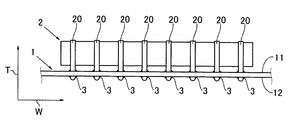
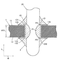
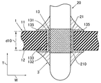
図1は本発明の一実施形態に係る電子回路装置について一部を省略して示す側側面図、図2は図1に示した電子回路装置について一部を拡大して示す端面図、図3は図2に示した電子回路装置についてさらに一部を拡大して示す端面図である。図1乃至図3を参照すると、本発明の一実施形態に係る電子回路装置は、回路基板1と、電子部品2と、はんだ3とを含む。
FIG. 1 is a side view showing a part of an electronic circuit device according to an embodiment of the present invention. FIG. 2 is an end view showing a part of the electronic circuit device shown in FIG. FIG. 3 is an end view showing a part of the electronic circuit device shown in FIG. 2 in an enlarged manner. 1 to 3, an electronic circuit device according to an embodiment of the present invention includes a
回路基板1は、この種の電子回路装置において広く用いられているプリント基板であって、好ましくは、一面11、及び、他面12のそれぞれの面内に電気回路を構成する導電パターン(図示しない)が形成されており、且、この導電パターンのリード部分に対応する箇所に、スルーホール13を有している。
The
スルーホール13は、内面133を有するとともに、回路基板1の一面11に第1の開口端131を有し、一面11に対向する他面12に第2の開口端132を有する。第1の開口端131の付近、第2の開口端132の付近、及び、内面133は、導体膜135により覆われている。
The through-
電子部品2は、IC、LSI、コンデンサ、コネクタなどの電子部品であって、これらの電子回路部(図示しない)と電気的に接続されている接続端子20を有し、回路基板1の一面11に載置されている。
The
接続端子20は、導電性金属材料でなる。図1乃至図3からは必ずしも明らかではないが、接続端子20は、平板状であって、先端部付近において、幅方向Wに向かい合う両端縁が切り欠かれた凹部21を有する。凹部21は、P1で示す凹形状の中央部から、P2、P3で示す両端部に向かうに従って、円弧状に湾曲する内面210を有する。
The
接続端子20は、凹部21が、スルーホール13の内部において、少なくとも回路基板1の厚みd10に対応する領域内に配置されている。図3を参照すると、凹部21の内面210と、導体膜135の表面との対面距離d11は、中央部P1で最も広くなり、P1を始点にして高さ方向Tに相対向する両端部P2、P3、即ち、回路基板1の一面11の側における端部P2、及び、他面12の側における端部P3の二方向に向かうに従って徐々に狭くなり、最終的に両端部P2及びP3のそれぞれにおいて、対面距離d12、d13が最も狭くなる。
In the
はんだ3は、スルーホール13の内部において、凹部21の内面210と、導体膜135の表面との間に充填されており、回路基板1と、接続端子20とを固着している。電子部品2は、接続端子20が、スルーホール13の内部において、導体膜135とはんだ3により結合されることにより、接続端子20を介して、回路基板1に固着され、且、回路基板1の上の導電パターン(図示しない)と電気的に接続される。
The
上述したように、本発明の一実施形態に係る電子回路装置において、接続端子20の凹部21がスルーホール13の内部に配置され、導体膜135の表面と、凹部21の内面210との間にはんだ3が充填されている構造によると、接続端子20と、回路基板1とを強固に結合することができる。
As described above, in the electronic circuit device according to the embodiment of the present invention, the
より詳細に説明すると、本発明の一実施形態に係る電子回路装置は、凹部21の内面210と、導体膜135の表面との間にはんだ3が充填されているから、回路基板1、及び、接続端子20のそれぞれに、振動、衝撃、及び、熱膨張/収縮等による機械的ストレスが生じたとしても、対面距離d12、d13が最も狭くなる両端部P2、P3で、両者を固着しているはんだ3の移動が規制される。例えば、接続端子20の熱膨張時において、接続端子20が一面11の方向に伸びようとした場合、はんだ3の移動が端部P3で制御されるため、接続端子20のズレ量が規制される。さらに、このような規制効果は、回路基板1の熱膨張時において、回路基板1が一面11の方向に伸びようとした場合にも、はんだ3の移動が端部P2で制御されるため、回路基板1のズレ量が規制される。従って、回路基板1と、接続端子20との結合状態を良好に維持し、はんだ3の剥離や、はんだ3に対するクラックの発生を回避することができる。
More specifically, in the electronic circuit device according to the embodiment of the present invention, the
しかも、はんだ3の移動に対する両端部P2、P3の規制効果は、回路基板1、及び、接続端子20の機械的ストレスが、一面11から他面12に向かう場合と、他面12から一面11に向かう場合との二方向に対しても生じるから、本発明の一実施形態に係る電子回路装置は優れた結合強度を有し、信頼性を向上させることができる。
Moreover, the restriction effect of the two end portions P2 and P3 on the movement of the
また、凹部21の内部に備えられる構成によると、凹部21を有しない端子と比較して、はんだ3接触面積が広がるから、結合強度を向上することができる。
Moreover, according to the structure provided in the inside of the recessed
接続端子20の凹部21は、中央部P1から端部P2、P3に向かうに従って狭くなる形状を有すれば足りるから、接続端子20の加工コストを低減し、優れた生産性を有する電子回路装置を提供することができる。
Since the
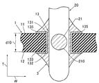
図4乃至図7は本発明の他の実施形態に係る電子回路装置について、一部を省略して示す端面図である。図4乃至図7において、図1乃至図3に示した構成部分と同一の構成部分には、同一の参照符号を付す。 4 to 7 are end views showing an electronic circuit device according to another embodiment of the present invention with a part thereof omitted. 4 to 7, the same components as those shown in FIGS. 1 to 3 are denoted by the same reference numerals.
図1乃至図3を参照して説明したように、本発明に係る電子部品2は、スルーホール13の内部において、凹部21の内面210と、導体膜135の表面との対面距離d11〜d13に広狭の差を有する内部空間を有し、この内部空間にはんだ3が充填されていることにより、はんだ3の移動が両端部P2、P3で規制され、はんだ3によって固着されている接続端子20、及び、回路基板1との結合強度を向上させることができる点に特徴がある。従って、凹部21は、中央部P1で最も広くなり、両端部P2、P3に向かうに従って徐々に狭くなる構造であればたりる。
As described with reference to FIGS. 1 to 3, the
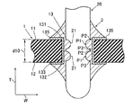
例えば、図4に示す電子回路装置の実施形態は、凹部21を、接続端子20の高さ方向Tに沿って複数配置した実施形態を示している。図4に示す実施形態の構造によると、図1乃至図3に示した利点を全て有するとともに、凹部21の内面210と、はんだ3との接触面積が増えるから、結合強度を向上することができる。
For example, the embodiment of the electronic circuit device shown in FIG. 4 shows an embodiment in which a plurality of the
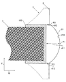
図5に示す電子回路装置の実施形態において、接続端子20は円筒状の棒状端子であり、この円筒状の接続端子20の先端部において、全周に渡って凹部21が溝状に形成されている。図5に示す実施形態の構造によると、図1乃至図3に示した利点を全て有するとともに、凹部21の内面210と、はんだ3との接触面積が増える。
In the embodiment of the electronic circuit device shown in FIG. 5, the
図6に示す電子回路装置の実施形態において、接続端子20の全周に渡って凹部21が備えられており、この凹部21はローレット加工により形成されている。端的に言うと、図6に示した実施形態は、図4に示した実施形態と、図5に示した実施形態の特徴部分を併せ持つ構造である。
In the embodiment of the electronic circuit device shown in FIG. 6, a
図7に示す電子回路装置の実施形態において、凹部21は、高さ方向T(接続端子20の軸方向)に直交する方向に接続端子20の基体部を貫通する貫通孔である。この構成によると、凹部21に充填されたはんだ3の移動を、内面210の全周に渡って規制することができる。
In the embodiment of the electronic circuit device shown in FIG. 7, the
以上、好ましい実施例を参照して本発明の内容を具体的に説明したが、本発明の基本的技術思想及び教示に基づいて、当業者であれば、種種の変形態様を採り得ることは自明である。 Although the contents of the present invention have been specifically described above with reference to the preferred embodiments, it is obvious that those skilled in the art can take various modifications based on the basic technical idea and teachings of the present invention. It is.
1 回路基板
11 一面
12 他面
13 スルーホール
133 内面
135 導体膜
2 電子部品
20 接続端子
21 凹部
220 内面
3 はんだ
DESCRIPTION OF
Claims (4)
前記回路基板は、一面から他面に貫通するスルーホールを有しており、
前記スルーホールは、内面に導体膜が備えられており、
前記電子部品は、接続端子を有し、前記回路基板の一面に載置されており、
前記接続端子は、凹部を有し、前記凹部は、前記スルーホールの内部に配置されており、
前記はんだは、前記スルーホールの内部において、少なくとも前記導体膜の表面と、前記凹部の内面との間に充填され、前記回路基板と、前記接続端子とを固着している、
電子回路装置。 An electronic circuit device including a circuit board, an electronic component, and solder,
The circuit board has a through hole penetrating from one surface to the other surface,
The through hole is provided with a conductor film on the inner surface,
The electronic component has a connection terminal and is placed on one surface of the circuit board,
The connection terminal has a recess, and the recess is disposed inside the through hole,
The solder is filled at least between the surface of the conductor film and the inner surface of the recess inside the through hole, and fixes the circuit board and the connection terminal.
Electronic circuit device.
前記凹部は、内面が弧状であり、両端部が前記スルーホールの開口端の付近に位置する、電子回路装置。 The electronic circuit device according to claim 1,
The concave portion has an arcuate inner surface, and both end portions are located in the vicinity of the opening end of the through hole.
前記凹部は、ローレット加工により形成されている、電子回路装置。 The electronic circuit device according to claim 1,
The recess is an electronic circuit device formed by knurling.
前記凹部は、貫通孔である、電子回路装置。
The electronic circuit device according to claim 1,
The electronic circuit device, wherein the recess is a through hole.
Priority Applications (1)
| Application Number | Priority Date | Filing Date | Title |
|---|---|---|---|
| JP2005316770A JP2007123718A (en) | 2005-10-31 | 2005-10-31 | Electronic circuit device |
Applications Claiming Priority (1)
| Application Number | Priority Date | Filing Date | Title |
|---|---|---|---|
| JP2005316770A JP2007123718A (en) | 2005-10-31 | 2005-10-31 | Electronic circuit device |
Publications (1)
| Publication Number | Publication Date |
|---|---|
| JP2007123718A true JP2007123718A (en) | 2007-05-17 |
Family
ID=38147204
Family Applications (1)
| Application Number | Title | Priority Date | Filing Date |
|---|---|---|---|
| JP2005316770A Pending JP2007123718A (en) | 2005-10-31 | 2005-10-31 | Electronic circuit device |
Country Status (1)
| Country | Link |
|---|---|
| JP (1) | JP2007123718A (en) |
Cited By (2)
| Publication number | Priority date | Publication date | Assignee | Title |
|---|---|---|---|---|
| CN102143658A (en) * | 2010-01-29 | 2011-08-03 | 欧姆龙株式会社 | Mounting component, electronic device and mounting method |
| JP2012038907A (en) * | 2010-08-06 | 2012-02-23 | Yazaki Corp | Terminal and soldering structure for the same |
Citations (4)
| Publication number | Priority date | Publication date | Assignee | Title |
|---|---|---|---|---|
| JPS61166563U (en) * | 1985-04-01 | 1986-10-16 | ||
| JPH0818192A (en) * | 1994-06-30 | 1996-01-19 | Meidensha Corp | Connection structure for printed board |
| JPH10241760A (en) * | 1997-02-24 | 1998-09-11 | Fujitsu Ltd | Insertion type pin-shaped terminal and circuit module having the same |
| JP2005150525A (en) * | 2003-11-18 | 2005-06-09 | Denso Corp | Structure and method for mounting terminal insertion type member |
-
2005
- 2005-10-31 JP JP2005316770A patent/JP2007123718A/en active Pending
Patent Citations (4)
| Publication number | Priority date | Publication date | Assignee | Title |
|---|---|---|---|---|
| JPS61166563U (en) * | 1985-04-01 | 1986-10-16 | ||
| JPH0818192A (en) * | 1994-06-30 | 1996-01-19 | Meidensha Corp | Connection structure for printed board |
| JPH10241760A (en) * | 1997-02-24 | 1998-09-11 | Fujitsu Ltd | Insertion type pin-shaped terminal and circuit module having the same |
| JP2005150525A (en) * | 2003-11-18 | 2005-06-09 | Denso Corp | Structure and method for mounting terminal insertion type member |
Cited By (2)
| Publication number | Priority date | Publication date | Assignee | Title |
|---|---|---|---|---|
| CN102143658A (en) * | 2010-01-29 | 2011-08-03 | 欧姆龙株式会社 | Mounting component, electronic device and mounting method |
| JP2012038907A (en) * | 2010-08-06 | 2012-02-23 | Yazaki Corp | Terminal and soldering structure for the same |
Similar Documents
| Publication | Publication Date | Title |
|---|---|---|
| JP4258432B2 (en) | Substrate bonding member and three-dimensional connection structure using the same | |
| JP4524291B2 (en) | Flat type ground terminal and its surface mounting method | |
| US20070224890A1 (en) | Contact for a battery connector | |
| CN1767279A (en) | Surface Mount Connector | |
| US10461447B2 (en) | Socket receiving an electronic component having a plurality of contact pads | |
| JP2021158225A (en) | Shield case and electronic circuit module | |
| CN100438218C (en) | Fixing member and fixing structure | |
| JP2014011210A (en) | Mounting structure of chip component | |
| JP2004319381A (en) | Grounding terminal | |
| US11096285B2 (en) | Electronic circuit substrate | |
| US6333471B1 (en) | Sheet metal component for double pattern conduction and printed circuit board | |
| JP2007123718A (en) | Electronic circuit device | |
| CN104685722B (en) | The grounding construction of circuit substrate | |
| JP2008288359A (en) | Printed circuit board | |
| US20060070768A1 (en) | Printed circuit board assembly | |
| JP4797781B2 (en) | Reinforcing tab, reinforcing tab manufacturing method, and connector mounting structure | |
| CN105830543A (en) | electronic components | |
| US20020005296A1 (en) | Surface mount package for long lead devices | |
| CN110636698B (en) | Circuit Board | |
| JPH11219762A (en) | Electronic components and substrates | |
| JP2006134946A (en) | Printed wiring board | |
| JPH11340589A (en) | Flexible circuit board | |
| CN102238837B (en) | Electronic apparatus | |
| JP2007116039A (en) | Circuit board | |
| JP2008066411A (en) | Electronic component mounting structure |
Legal Events
| Date | Code | Title | Description |
|---|---|---|---|
| A621 | Written request for application examination |
Free format text: JAPANESE INTERMEDIATE CODE: A621 Effective date: 20080603 |
|
| RD04 | Notification of resignation of power of attorney |
Free format text: JAPANESE INTERMEDIATE CODE: A7424 Effective date: 20090217 |
|
| A977 | Report on retrieval |
Free format text: JAPANESE INTERMEDIATE CODE: A971007 Effective date: 20100921 |
|
| A131 | Notification of reasons for refusal |
Free format text: JAPANESE INTERMEDIATE CODE: A131 Effective date: 20100929 |
|
| A02 | Decision of refusal |
Free format text: JAPANESE INTERMEDIATE CODE: A02 Effective date: 20110209 |