JP2007019109A - Film formation method, and manufacturing method of semiconductor device - Google Patents
Film formation method, and manufacturing method of semiconductor device Download PDFInfo
- Publication number
- JP2007019109A JP2007019109A JP2005196731A JP2005196731A JP2007019109A JP 2007019109 A JP2007019109 A JP 2007019109A JP 2005196731 A JP2005196731 A JP 2005196731A JP 2005196731 A JP2005196731 A JP 2005196731A JP 2007019109 A JP2007019109 A JP 2007019109A
- Authority
- JP
- Japan
- Prior art keywords
- film
- target
- chamber
- forming
- magnet unit
- Prior art date
- Legal status (The legal status is an assumption and is not a legal conclusion. Google has not performed a legal analysis and makes no representation as to the accuracy of the status listed.)
- Granted
Links
Images


Abstract
Description
本発明は、成膜方法及び半導体装置の製造方法に関する。 The present invention relates to a film forming method and a semiconductor device manufacturing method.
電源を切っても情報を記憶することができる不揮発性メモリとして、フラッシュメモリや強誘電体メモリが知られている。 Flash memories and ferroelectric memories are known as nonvolatile memories that can store information even when the power is turned off.
このうち、フラッシュメモリは、絶縁ゲート型電界効果トランジスタ(IGFET)のゲート絶縁膜中に埋め込んだフローティングゲートを有し、記憶情報を表す電荷をこのフローティングゲートに蓄積することによって情報を記憶する。しかし、このようなフラッシュメモリでは、情報の書き込みや消去の際に、ゲート絶縁膜にトンネル電流を流す必要があり、比較的高い電圧が必要であるという欠点がある。 Among these, the flash memory has a floating gate embedded in a gate insulating film of an insulated gate field effect transistor (IGFET), and stores information by accumulating charges representing stored information in the floating gate. However, such a flash memory has a drawback that a tunnel current needs to flow through the gate insulating film when writing or erasing information, and a relatively high voltage is required.
これに対し、強誘電体メモリは、FeRAM(Ferroelectric Random Access Memory)とも呼ばれ、強誘電体キャパシタが備える強誘電体膜のヒステリシス特性を利用して情報を記憶する。その強誘電体膜は、キャパシタの上部電極と下部電極の間に印加される電圧に応じて分極を生じ、その電圧を取り去っても自発分極が残留する。印加電圧の極性を反転すると、この自発分極も反転し、その自発分極の向きを「1」と「0」に対応させることで、強誘電体膜に情報が書き込まれる。この書き込みに必要な電圧はフラッシュメモリにおけるよりも低く、また、フラッシュメモリよりも高速で書き込みができるという利点がFeARMにはある。 On the other hand, the ferroelectric memory is also called FeRAM (Ferroelectric Random Access Memory), and stores information using the hysteresis characteristic of the ferroelectric film provided in the ferroelectric capacitor. The ferroelectric film is polarized according to the voltage applied between the upper electrode and the lower electrode of the capacitor, and the spontaneous polarization remains even if the voltage is removed. When the polarity of the applied voltage is reversed, this spontaneous polarization is also reversed, and the direction of the spontaneous polarization is made to correspond to “1” and “0”, whereby information is written in the ferroelectric film. FeARM has the advantage that the voltage required for this writing is lower than that in the flash memory and that writing can be performed at a higher speed than the flash memory.
このFeRAMのキャパシタの上部電極は、非特許文献1、2に開示されるように、プラチナ(Pt)等の貴金属で構成される場合が多い。また、キャパシタの疲労特性や信頼性を改善するために、酸化物で上部電極を構成することもある。その酸化物としては、非特許文献4に開示されるIrO2や、特許文献5、6に開示されるSRO(SrRuO3)がある。 The upper electrode of this FeRAM capacitor is often composed of a noble metal such as platinum (Pt), as disclosed in Non-Patent Documents 1 and 2. Further, in order to improve the fatigue characteristics and reliability of the capacitor, the upper electrode may be made of an oxide. Examples of the oxide include IrO 2 disclosed in Non-Patent Document 4 and SRO (SrRuO 3 ) disclosed in Patent Documents 5 and 6.
一方、キャパシタ誘電体膜は、PZT(Lead Zirconate Titanate)や、PZTにランタンをドープしたPLZT等のPZT系材料で構成されるのが一般的である。或いは、SrBi2Ta2O9(SBT, Y1)やSrBi2(Ta, Nb)2O9(SBTN, YZ)等のBi層状構造化合物もキャパシタ誘電体膜の材料として利用される。 On the other hand, the capacitor dielectric film is generally made of a PZT material such as PZT (Lead Zirconate Titanate) or PLZT in which PZT is doped with lanthanum. Alternatively, Bi layer structure compounds such as SrBi 2 Ta 2 O 9 (SBT, Y1) and SrBi 2 (Ta, Nb) 2 O 9 (SBTN, YZ) are also used as the material of the capacitor dielectric film.
これらの材料のうち、PZT系材料でキャパシタ誘電体膜を構成する場合には、膜中におけるZrとTiの和に対するPbの比率(Pb/(Zr+Ti))が、キャパシタ誘電体膜の電気特性に大きな影響を与えることが知られている。例えば、上記した非特許文献4では、Pb/(Zr+Ti)の値により、キャパシタのスイッチング電荷やリーク電流が変化することが開示されている。 Among these materials, when the capacitor dielectric film is composed of PZT-based materials, the ratio of Pb to the sum of Zr and Ti (Pb / (Zr + Ti)) in the film is the electric capacity of the capacitor dielectric film. It is known to have a great influence on characteristics. For example, Non-Patent Document 4 described above discloses that the switching charge and leakage current of a capacitor change depending on the value of Pb / (Zr + Ti).
従って、PZT系材料を用いて強誘電体メモリを量産するには、Pb/(Zr+Ti)の値(以下、Pb量ともいう)が半導体ウエハ間でばらつかずに所望の値になるようにし、強誘電体キャパシタの特性が各半導体ウエハにおいて一定になるようにする必要がある。 Therefore, to mass-produce ferroelectric memories using PZT-based materials, the value of Pb / (Zr + Ti) (hereinafter also referred to as Pb amount) does not vary between semiconductor wafers and becomes a desired value. Therefore, it is necessary to make the characteristics of the ferroelectric capacitor constant in each semiconductor wafer.
ところが、スパッタ法により強誘電体膜を形成する場合、キャパシタ誘電体膜のPb量をコントロールするのは非常に困難である。例えば、非特許文献7には、一つのスパッタチャンバにおいて数10枚程度の半導体ウエハに連続してPZT膜を形成しただけで、PZT膜におけるPb量が半導体ウエハ間で大きく変動することが開示されている。この点に鑑み、非特許文献7では、スパッタガスであるArガスの流量を調節することで、PZT膜におけるPb量を制御することを提案している。 However, when a ferroelectric film is formed by sputtering, it is very difficult to control the amount of Pb in the capacitor dielectric film. For example, Non-Patent Document 7 discloses that the amount of Pb in a PZT film varies greatly between semiconductor wafers only by forming a PZT film continuously on several tens of semiconductor wafers in one sputter chamber. ing. In view of this point, Non-Patent Document 7 proposes to control the amount of Pb in the PZT film by adjusting the flow rate of Ar gas, which is a sputtering gas.
一方、非特許文献8には、半導体ウエハが載置されるウエハステージを電気的にフローティングにすると共に、マグネトロンスパッタ法で使用される磁石の形を改良することで、マグネトロンスパッタ法で形成されたPZT膜におけるPb量の制御性を改善することが開示されている。その結果、非特許文献8によれば、半導体ウエハの面内におけるPb量の分布と、半導体ウエハ間でのPb量の分布とが改善され、一つのマグネトロンスパッタチャンバを用いてPZT膜を形成しても、約80日間にわたって膜中のPb量を安定させることができるとある。 On the other hand, in Non-Patent Document 8, the wafer stage on which the semiconductor wafer is placed is electrically floating, and the shape of the magnet used in the magnetron sputtering method is improved, so that it is formed by the magnetron sputtering method. It is disclosed to improve the controllability of the Pb amount in the PZT film. As a result, according to Non-Patent Document 8, the distribution of the Pb amount in the surface of the semiconductor wafer and the distribution of the Pb amount between the semiconductor wafers are improved, and a PZT film is formed using one magnetron sputtering chamber. However, the amount of Pb in the film can be stabilized for about 80 days.
なお、ウエハステージをフローティングにしてPb量の分布を改善する点については特許文献1にも開示されている。 Note that Patent Document 1 discloses that the Pb amount distribution is improved by floating the wafer stage.
ところで、マグネトロンスパッタチャンバには、上記したウエハステージの他に、PZTよりなるターゲットと、スパッタされたPZTがチャンバの内面に付着するのを防止するためのシールドが設けられる。 Incidentally, in addition to the wafer stage described above, the magnetron sputtering chamber is provided with a target made of PZT and a shield for preventing the sputtered PZT from adhering to the inner surface of the chamber.
このうち、ターゲットは、成膜を続けるにつれてその厚さがエロージョンにより薄くなるので、新品として納入してからある程度の期間が経過した後には、再び新品に交換する必要がある。また、シールドも、成膜によってその表面にPZTが堆積し、その堆積厚が厚くなり過ぎるとPZTが剥離してパーティクルの原因になるので、やはりある程度の期間を見て新品に交換する必要がある。 Among these targets, the thickness of the target becomes thinner due to erosion as the film is formed. Therefore, it is necessary to replace the target with a new one after a certain period of time has passed since it was delivered as a new one. Also, PZT is deposited on the surface of the shield by film formation, and if the deposition thickness becomes too thick, PZT peels off and causes particles, so it is necessary to replace it with a new one after a certain period of time. .
このように、ターゲットとシールドはいずれも消耗品であり、新品の状態からそれらが使用不可になるまでの期間は寿命と呼ばれる。シールドの寿命は、典型的には数週間であり、これは半導体ウエハを数100枚〜数1000毎だけ処理した期間に相当する。また、ターゲットの寿命は数ヶ月であり、これは半導体ウエハの処理枚数に換算すると数1000毎〜10000枚となる。 Thus, both the target and the shield are consumables, and the period from when they are new to when they become unusable is called the lifetime. The life of the shield is typically several weeks, which corresponds to a period of processing several hundred to several thousand semiconductor wafers. Further, the life of the target is several months, which is every several thousand to 10,000 in terms of the number of processed semiconductor wafers.
このように、ターゲットとシールドの寿命は、非特許文献8が膜中のPb量を保証する80日間よりもはるかに長い。従って、非特許文献8の方法では、ターゲットやシールドが寿命を迎える前にPZT膜のPb量が変動し始めるので、Pb量を元に戻すために上記の80日程度を目安にターゲットとシールドを新品に交換する必要がある。これにより、ターゲットとシールドを有効に利用することができないと共に、ターゲットとシールドのコストがFeRAMの製造コストに転嫁され、安価なFeRAMを市場に供給することができなくなる。 Thus, the lifetime of the target and the shield is much longer than 80 days when Non-Patent Document 8 guarantees the amount of Pb in the film. Therefore, in the method of Non-Patent Document 8, the Pb amount of the PZT film starts to fluctuate before the target or shield reaches the end of its life. It needs to be replaced with a new one. As a result, the target and shield cannot be used effectively, and the cost of the target and shield is transferred to the manufacturing cost of FeRAM, so that inexpensive FeRAM cannot be supplied to the market.
また、非特許文献8には、磁石を変更することでPb量の面内分布をコントロールできるとあるので、ターゲット使用量に応じて別の磁石に交換することも考えられる。しかし、ターゲット使用量に応じて何種類もの磁石を設計、製作するのは時間とコストがかかるため好ましくない。更に、磁石の交換を頻繁に行うことは、手間が掛かると共に、生産ラインの生産性を悪化させるので、現実的でない。しかも、磁石を交換したからといってチャンバ内の磁場の状態が元に戻るとは限らないので、磁石の交換がPb量の分布を改善するとは限らない。
本発明の目的は、Pb量の面内分布が変動するのを防止することが可能な成膜方法及び半導体装置の製造方法を提供することにある。 An object of the present invention is to provide a film forming method and a semiconductor device manufacturing method capable of preventing the in-plane distribution of the Pb amount from fluctuating.
本発明の一観点によれば、チャンバと、該チャンバの内部に設けられた鉛を含むスパッタターゲットと、前記チャンバの外側に回転可能な状態で設けられて前記スパッタターゲットの表面の磁場を時間的に変動させる磁石ユニットとを有するマグネトロンスパッタ装置を用い、マグネトロンスパッタ法による鉛を含んだ膜の成膜が所定枚数の基板に対して終了するたびに、前記スパッタターゲットと前記磁石ユニットのそれぞれの表面同士の距離を最適距離に戻す成膜方法が提供される。 According to an aspect of the present invention, a chamber, a sputter target containing lead provided inside the chamber, and a magnetic field on the surface of the sputter target provided in a rotatable state outside the chamber are temporally changed. Each time the deposition of the lead-containing film by the magnetron sputtering method is completed on a predetermined number of substrates, the surface of each of the sputter target and the magnet unit is used. There is provided a film forming method for returning the distance between them to an optimum distance.
本発明に係る成膜方法によれば、所定枚数の基板に対して成膜を行った後、スパッタターゲットと磁石ユニットのそれぞれの表面同士の距離が最適距離に戻されるので、スパッタターゲットの表面付近での磁場の状態が一定に保たれ、膜中に含まれる鉛の比率の面内分布が磁場の変動によって悪化するのを防止できる。 According to the film forming method of the present invention, after the film is formed on a predetermined number of substrates, the distance between the surfaces of the sputter target and the magnet unit is returned to the optimum distance. Thus, it is possible to prevent the in-plane distribution of the ratio of lead contained in the film from being deteriorated by fluctuations in the magnetic field.
また、本発明の別の観点によれば、半導体基板の上に下地絶縁膜を形成する工程と、前記下地絶縁膜の上に第1導電膜を形成する工程と、前記第1導電膜の上に、マグネトロンスパッタ法により鉛を含む強誘電体膜を形成する工程と、前記強誘電体膜の上に第2導電膜を形成する工程と、前記第1導電膜、前記強誘電体膜、及び前記第2導電膜をパターニングすることにより、下部電極、キャパシタ誘電体膜、及び上部電極で構成されるキャパシタを形成する工程とを有し、前記強誘電体膜を形成する工程において、チャンバと、該チャンバの内部に設けられた鉛を含むスパッタターゲットと、前記チャンバの外側に回転可能な状態で設けられて前記スパッタターゲットの表面の磁場を時間的に変動させる磁石ユニットとを有するマグネトロンスパッタ装置を用い、前記強誘電体膜の成膜が所定枚数の前記半導体基板に対して終了するたびに、前記スパッタターゲットと前記磁石ユニットのそれぞれの表面同士の距離を最適距離に戻す半導体装置の製造方法が提供される。 According to another aspect of the present invention, a step of forming a base insulating film on a semiconductor substrate, a step of forming a first conductive film on the base insulating film, A step of forming a ferroelectric film containing lead by magnetron sputtering, a step of forming a second conductive film on the ferroelectric film, the first conductive film, the ferroelectric film, and Forming a capacitor composed of a lower electrode, a capacitor dielectric film, and an upper electrode by patterning the second conductive film, and in the step of forming the ferroelectric film, a chamber; A magnetron having a sputter target containing lead provided inside the chamber and a magnet unit which is provided outside the chamber so as to be rotatable and changes the magnetic field on the surface of the sputter target with time. A semiconductor device that uses a sputtering apparatus to return the distance between the surfaces of the sputtering target and the magnet unit to an optimum distance each time film formation of the ferroelectric film is completed on a predetermined number of the semiconductor substrates. A manufacturing method is provided.
本発明に係る半導体装置の製造方法によれば、所定枚数の半導体基板に対して強誘電体膜の成膜が終了するたびに、スパッタターゲットと磁石ユニットのそれぞれの表面同士の距離を最適距離に戻すので、次回以降の半導体基板に対して強誘電体膜を形成する場合でも、その強誘電体膜における鉛の比率の面内分布を常に一様に保つことができ、キャパシタの特性が常に安定した半導体装置を量産することが可能となる。 According to the method for manufacturing a semiconductor device of the present invention, the distance between the surfaces of the sputter target and the magnet unit is set to the optimum distance every time the ferroelectric film is formed on a predetermined number of semiconductor substrates. Therefore, even when a ferroelectric film is formed on the next and subsequent semiconductor substrates, the in-plane distribution of the lead ratio in the ferroelectric film can always be kept uniform, and the capacitor characteristics are always stable. It becomes possible to mass-produce the semiconductor device.
本発明によれば、鉛を含んだ膜の成膜が所定枚数の基板に対して終了するたびに、スパッタターゲットと磁石ユニットのそれぞれの表面同士の距離を最適距離に戻すので、スパッタターゲットの表面付近での磁場の状態が一定に保たれ、膜中に含まれる鉛の比率の面内分布が磁場の変動によって悪化するのを防止することが可能となる。 According to the present invention, every time film formation containing lead is completed for a predetermined number of substrates, the distance between the surfaces of the sputter target and the magnet unit is returned to the optimum distance. The state of the magnetic field in the vicinity is kept constant, and it is possible to prevent the in-plane distribution of the ratio of lead contained in the film from being deteriorated by the fluctuation of the magnetic field.
以下に、本発明の実施の形態について、添付図面を参照しながら詳細に説明する。 Hereinafter, embodiments of the present invention will be described in detail with reference to the accompanying drawings.
(1)予備的事項の説明
本実施形態の説明に先立ち、本発明の予備的事項について説明する。
(1) Description of Preliminary Items Prior to the description of the present embodiment, preliminary items of the present invention will be described.
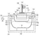
図1は、株式会社アルバック製のPZTスパッタ装置であるCERAUS-ZX-1000の構成図である。 FIG. 1 is a configuration diagram of CERAUS-ZX-1000 which is a PZT sputtering apparatus manufactured by ULVAC, Inc.
そのスパッタ装置は、RFマグネトロンスパッタ法により成膜を行うためのチャンバ101を有し、シリコン基板10が載せられるウエハステージ(基板載置台)102がそのチャンバ101の下部に設けられる。ウエハステージ102の上方には、ステンレスよりなるシールド103が配され、スパッタされた材料がチャンバ101の内壁に付着するのがこのシールド103によって防がれる。
The sputtering apparatus has a
更に、このシールド103の上方には、チャンバ101の上部を塞ぐ銅よりなるバッキングプレート105が配され、バッキングプレート105とチャンバ101との間のOリング117によってチャンバ101内が気密に保たれる。そのバッキングプレート105は、不図示のIn(インジウム)ボンディング材によって、PZTの焼結体よりなるスパッタターゲット104を保持する役割も担う。
Further, above the
スパッタターゲット104のサイズは特に限定されないが、本実施形態では、その直径を300mm、厚さを4mmとする。また、スパッタターゲット104の材料は鉛を含むものであればPZTに限定されず、PZTにランタンをドープしたPLZTよりなるスパッタターゲット104を用いてもよい。
The size of the
そして、バッキングプレート105には、周波数が13.56MHzの高周波電源116が接続され、該高周波電源116から供給された高周波電力によってチャンバ101内のスパッタガスがプラズマ化される。
A high
バッキングプレート105の上には樹脂板114が固定されており、第1プーリ118を回転させるための第1モータ113がその樹脂板114上に固定される。更に、バッキングプレート105の上方には、例えば8本のネジ(不図示)によって、テフロン板107を介して磁石ユニット106が回転板108に固定される。
A
第1モータ113で発生した回転駆動力は、第1プーリ118、動力ベルト115、及び第2プーリ109によって回転板108に伝えられ、これにより回転板108に固定されている磁石ユニット106が回転し、スパッタターゲット104の表面104aでの磁場が時間的に変動することになる。
The rotational driving force generated by the
次に、このスパッタ装置を用いて本願発明者が行った実験について説明する。 Next, an experiment conducted by the present inventor using this sputtering apparatus will be described.
図2は、この実験で使用したサンプルの断面図である。 FIG. 2 is a cross-sectional view of the sample used in this experiment.
そのサンプルを作成するには、まず、シリコン基板10の表面に熱酸化膜70を形成する。次いで、厚さ150nmのPr(プラチナ)膜と厚さ20nmのALO(アルミナ)膜とをこの順に積層してなる下部電極用導電膜71を形成し、図1のスパッタ装置を用いて、下部電極用導電膜71の上にPZT膜72を形成する。本願発明者は、このようにして形成されたPZT膜72におけるPb量の面内分布が、磁石ユニット106とスパッタターゲット104のそれぞれの表面同士の距離D(図1参照)にどのように依存するのかを以下のようにして調査した。
In order to prepare the sample, first, a thermal oxide film 70 is formed on the surface of the
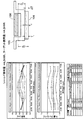
図3の左側に示す二つのグラフは、使用量が652.5kWhでほぼ限界(寿命)に達したスパッタターゲット104を用いて上記のPZT膜72を形成した場合におけるPZT膜72の膜厚とPb量のそれぞれの面内分布を示すものである。なお、スパッタターゲット104の使用量とは、スパッタターゲット104に供給された高周波電力の電力量の総和を指し、これについてはシールド103も同様である。
The two graphs shown on the left side of FIG. 3 show the film thickness and Pb of the
但し、PZT膜72のPb量の測定には、株式会社テクノス製の蛍光X線ウエハ表面分析装置であるSMAT2200を使用した。そして、シリコン基板10におけるPb量と膜厚の測定ポイントとしては、図6のような9ポイントを選択した。
However, for the measurement of the Pb amount of the
図3の右側に模式的に示されるように、このように使い古されたスパッタターゲット104では、エロージョンによってその表面が削られ、その厚さTfが新品の際の厚さTiよりもΔTだけ薄くなる。この例では、ΔTは3mmである。但し、エロージョンによる削れ量はターゲット104において不均一なので、本実施形態では、エロージョンによって最も深く削れた部分の削れ量をΔTとする
そして、このようなエロージョンによって、スパッタターゲット104が新品のときと比較して、磁石ユニット106とスパッタターゲット104との距離Dfが縮まることになる。この例では、ターゲット104が新品のときの距離Diは40mmであり、上記のDfは37mm(=Di−ΔT)となる。
As schematically shown on the right side of FIG. 3, the surface of the
また、PZT膜72の成膜条件としては、高周波電力116のパワー1.0kW、成膜時間273秒、圧力1.0Pa、基板温度50℃が採用された。そして、このような条件を用い、スパッタガスであるアルゴンガスの流量が15sccm、18sccm、20sccm、22sccmのそれぞれの場合について、PZT膜72の膜厚とPb量の面内分布とを測定した。
Further, as the film forming conditions for the
図3の左下のグラフに示されるように、このように使い込まれたターゲット104を用いると、Pb量の面内分布が一様となり、量産に適したPZT膜72が得られることが分かる。例えば、アルゴン流量が20sccmのとき、Pb量の面内における最大値と最小値との差は0.010となり、Pbの分布は極めて良好である。
As shown in the lower left graph of FIG. 3, it can be seen that when the
一方、図4は、スパッタターゲット104を新品(使用量44.2kWh)に交換し、図3の場合と同じ条件でPZT膜72を形成して、そのPZT膜72の膜厚とPb量の面内分布を調査して得られたグラフである。
On the other hand, FIG. 4 shows that the
この場合、新品のスパッタターゲット104にエロージョンは発生していないので、磁石ユニット106とスパッタターゲット104との距離は初期値であるDi(=40mm)となり、図3の場合よりも長くなる。
In this case, since erosion does not occur in the
図4に示されるように、このようにスパッタターゲット104を新品に交換すると、Pb量の面内分布が図3の場合よりも悪化する。例えば、アルゴン流量が20sccmの場合では、Pb量の最大値と最小値の差が0.022であり、図4の0.010の二倍程度の値になってしまう。
As shown in FIG. 4, when the
更に、Pb量の面内平均値についても、図4の場合よりも全体的に小さい値となってしまう。 Furthermore, the in-plane average value of the Pb amount also becomes a smaller value as a whole than in the case of FIG.
このようなPb量の面内分布の悪化は、磁石ユニット106とスパッタターゲット104との距離が図3の場合よりも長くなったことに原因があると考えられる。
Such a deterioration of the in-plane distribution of the Pb amount is considered to be caused by the fact that the distance between the
そこで、本願発明者は、図4の磁石ユニット106をスパッタターゲットに3mm近づけることにより、磁石ユニット106とスパッタターゲット104との距離を図3と同じDf(=37mm)に縮めて、改めてPZT膜72を形成した。そして、これにより得られたPZT膜に対し、図3、図4と同じ測定を行った。その結果を図5に示す。
Therefore, the inventor of the present application reduces the distance between the
図5に示されるように、Pb量の面内分布は、図4の場合よりも平坦になり、図3と同様な均一性を呈するようになった。例えば、アルゴン流量が20sccmでは、Pb量の面内における最大値と最小値との差は0.012となり、図3における0.010に近い値となった。 As shown in FIG. 5, the in-plane distribution of the Pb amount is flatter than that in FIG. 4 and exhibits the same uniformity as in FIG. For example, when the argon flow rate is 20 sccm, the difference between the maximum value and the minimum value of the Pb amount in the plane is 0.012, which is close to 0.010 in FIG.
図3〜図5の実験結果より、RFマグネトロンスパッタ法によりPZT膜を形成する場合は、磁石ユニット106とスパッタターゲット104との距離によって、PZT膜におけるPb量の面内分布が変動することが明らかとなった。これは、上記の距離により、スパッタターゲット104の表面付近での磁場の状態が変わることに理由があると考えられる。
From the experimental results of FIGS. 3 to 5, it is clear that when the PZT film is formed by the RF magnetron sputtering method, the in-plane distribution of the Pb amount in the PZT film varies depending on the distance between the
(2)本発明の実施の形態
(i)成膜装置の説明
図7は、本実施形態で使用される成膜装置の構成図である。なお、図7において、図1と同じ要素には図1と同じ符号を付し、以下ではその説明を省略する。
(2) Embodiment of the Invention (i) Description of Film Forming Apparatus FIG. 7 is a configuration diagram of a film forming apparatus used in the present embodiment. 7, the same elements as those in FIG. 1 are denoted by the same reference numerals as those in FIG. 1, and description thereof is omitted below.
図7に示される成膜装置は、図1で説明した装置に磁石移動機構120を設けてなる。その磁石移動機構120は、第2プーリ109上に、該第2プーリ109の回転運動から独立したラック112を有し、ピニオンギア111がそのラックに嵌合する。そして、ピニオンギア111は、不図示の固定部材によって既述の樹脂板114に固定された第2モータ110に繋がっており、第2モータ110の回転運動がラック112とピニオンギア111によって上下運動に変換され、それにより磁石ユニット106が1mm程度の単位で連続的に昇降可能となっている。
The film forming apparatus shown in FIG. 7 is provided with a
磁石ユニット106のこのような昇降運動によって、この成膜装置では、スパッタターゲット104と磁石ユニット106のそれぞれの表面同士の距離Dを連続的に調節することができる。
By such an up-and-down movement of the
(ii)成膜方法の説明
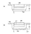
図8(a)、(b)は、図7の成膜装置を用いて行われる成膜方法を模式的に示す断面図である。
(Ii) Description of Film Formation Method FIGS. 8A and 8B are cross-sectional views schematically showing a film formation method performed using the film formation apparatus of FIG.
図8(a)は、スパッタターゲット104が新品のときの断面図である。この場合、スパッタターゲット104の厚さは初期値のTiであり、エロージョンによる薄厚化は無い。この状態で、既述の磁石移動機構120によって、スパッタターゲット104と磁石ユニット106のそれぞれの表面同士の距離Dを変えながら、何枚かのシリコン基板10に試験的にPZT膜を形成する。そして、それぞれのPZT膜のPb量の面内分布を調査し、分布が最も良好になったときのターゲット104と磁石ユニット106との距離を最適距離D0として求めておく。
FIG. 8A is a cross-sectional view when the
既述のように、スパッタターゲット104は、成膜を行う度にエロージョンによってその厚さが僅かずつ薄くなる。その結果、ターゲット104と磁石ユニット106との距離が最適距離D0から除々に短くなり、PZT膜のPb量の面内分布が悪化する恐れがある。
As described above, the thickness of the
そこで、本実施形態では、図8(b)に示すように、所定枚数、例えば1ロットを構成する25枚のシリコン基板10に対してPZT膜を形成した後に、ターゲット104の厚さの減少分ΔTだけ磁石移動機構120によって磁石ユニット106を上方に移動し、ターゲット104と磁石ユニット106との距離を最適距離D0に保つようにする。なお、磁石移動機構120の制御は、オペレータが手動で行ってもよいし、コンピュータにより自動で行ってもよい。
Therefore, in the present embodiment, as shown in FIG. 8B, after the PZT film is formed on a predetermined number, for example, 25
これによれば、ターゲット104の表面付近での磁場の状態が常に一定に保たれるので、磁場の変動に伴ってPb量の面内分布が悪化するのを防止できる。更に、この方法では、シールド103やスパッタターゲット104が寿命を迎えるまでの数週間〜数ヶ月の間の長期にわたり、ターゲット104と磁石ユニット106との距離が最適距離D0に保たれるので、80日間だけPb量を保証する非特許文献8と比較して、シールド103とスパッタターゲット104とを無駄にすることなく有効利用することができる。
According to this, since the state of the magnetic field in the vicinity of the surface of the
なお、上記では、所定枚数のシリコン基板10に対してPZT膜を成膜した後に磁石ユニット104を上方に移動させたが、これに代えて、一枚のシリコン基板10にPZT膜を成膜している最中に磁石ユニット106を移動し、ターゲット104と磁石ユニット106との距離を最適距離D0に保つようにしてもよい。
In the above description, the
ところで、アルミニウム膜等の金属膜用のスパッタ装置では、ターゲットのエロージョンによって金属膜の膜厚の面内分布が変動することが知られており、その面内分布を改善する目的で、適当な時期を見計らってターゲットと磁石ユニットとの距離を調節することが行われている。金属膜用のターゲット、例えばアルミターゲットは、その厚さが10mmや15mmと厚いものが一般的なため、金属膜用のスパッタ装置に付属の磁石ユニットの移動機構は、5mm単位での荒い移動しか行えないのが普通である。 By the way, in sputtering apparatuses for metal films such as aluminum films, it is known that the in-plane distribution of the film thickness of the metal film fluctuates due to erosion of the target. The distance between the target and the magnet unit is adjusted in view of the above. Since metal film targets, such as aluminum targets, are typically as thick as 10 mm or 15 mm, the moving mechanism of the magnet unit attached to the sputtering apparatus for metal films can only move roughly in units of 5 mm. It is normal not to be able to do it.
これに対し、PZT用のスパッタターゲット104は、PZTの焼結によって製造されるため、その厚さを上記の10mmや15mmのように厚くするのが技術的に困難であり、通常は4mm程度と薄い。よって、金属膜用のスパッタ装置の磁石ユニットの移動機構を本実施形態に流用したのでは、スパッタターゲット104と磁石ユニット106との距離を微細にコントロールするのが困難であり、その距離を最適距離D0に保つのが困難となる。
On the other hand, since the
更に、金属膜用のスパッタ装置では、上記のように膜厚の面内分布を調整するために磁石ユニットを移動させることが行われているが、スパッタされた膜の組成を変化させるという目的で磁石ユニットを移動させることは従来行われていない。 Further, in the sputtering apparatus for metal films, the magnet unit is moved in order to adjust the in-plane distribution of film thickness as described above, but for the purpose of changing the composition of the sputtered film. Conventionally, the magnet unit is not moved.
(iii)半導体装置の製造方法の説明
次に、上記で説明した成膜方法を用いた半導体装置の製造方法について説明する。以下では、半導体装置として、プレーナ型のFeRAMを製造する。
(Iii) Description of Semiconductor Device Manufacturing Method Next, a semiconductor device manufacturing method using the film forming method described above will be described. In the following, a planar type FeRAM is manufactured as a semiconductor device.
図9〜図14は、このFeRAMの製造途中の断面図である。 9 to 14 are cross-sectional views of the FeRAM being manufactured.
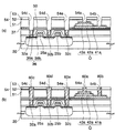
まず、図9(a)に示す断面構造を得るまでの工程を説明する。 First, steps required until a sectional structure shown in FIG.
最初に、n型又はp型のシリコン(半導体)基板20表面に、トランジスタの活性領域を画定するSTI(Shallow Trench Isolation)用の溝を形成し、その中に酸化シリコン等の絶縁膜を埋め込んで素子分離絶縁膜21とする。なお、素子分離構造はSTIに限られず、LOCOS(Local Oxidation of Silicon)法で素子分離絶縁膜21を形成してもよい。
First, a trench for STI (Shallow Trench Isolation) that defines an active region of a transistor is formed on the surface of an n-type or p-type silicon (semiconductor)
次いで、シリコン基板20の活性領域にp型不純物を導入してpウェル22を形成した後、その活性領域の表面を熱酸化することにより、ゲート絶縁膜28となる熱酸化膜を形成する。
Next, a p-type impurity is introduced into the active region of the
続いて、シリコン基板20の上側全面に非晶質又は多結晶のシリコン膜及びタングステンシリサイド膜を順に形成し、これらの膜をフォトリソグラフィによりパターニングしてゲート電極25a、25bを形成する。
Subsequently, an amorphous or polycrystalline silicon film and a tungsten silicide film are sequentially formed on the entire upper surface of the
pウェル22上には、上記の2つのゲート電極25a、25bが間隔をおいてほぼ平行に配置され、それらのゲート電極25a、25bはワード線の一部を構成する。
On the p-well 22, the two
次いで、ゲート電極25a、25bをマスクにするイオン注入により、各ゲート電極25a、25bの横のシリコン基板20にn型不純物を導入し、第1〜第3ソース/ドレインエクステンション24a〜24cを形成する。
Next, n-type impurities are introduced into the
その後に、シリコン基板20の上側全面に絶縁膜を形成し、その絶縁膜をエッチバックしてゲート電極25a、25bの横に絶縁性サイドウォール26として残す。その絶縁膜として、例えばCVD法により酸化シリコン膜を形成する。
After that, an insulating film is formed on the entire upper surface of the
続いて、絶縁性サイドウォール26とゲート電極25a、25bをマスクにしながら、シリコン基板20にn型不純物を再度イオン注入することにより、各ゲート電極25a、25bの側方のシリコン基板20に第1〜第3ソース/ドレイン領域23a〜23cを形成する。
Subsequently, the n-type impurity is ion-implanted again into the
ここまでの工程により、シリコン基板20の活性領域には、ゲート絶縁膜28、ゲート電極25a、25b、及び第1〜第3ソース/ドレイン領域23a〜23cによって構成される第1、第2MOSトランジスタTR1、TR2が形成されたことになる。
Through the above steps, the active region of the
次に、シリコン基板20の上側全面に、スパッタ法によりコバルト層等の高融点金属層を形成した後、この高融点金属層を加熱してシリコンと反応させ、シリコン基板20上に高融点金属シリサイド層27を形成する。その高融点金属シリサイド層27はゲート電極25a、25bの表層部分にも形成され、それにより各ゲート電極25a、25bが低抵抗化されることになる。
Next, after a refractory metal layer such as a cobalt layer is formed on the entire upper surface of the
その後、素子分離絶縁膜21の上等で未反応となっている高融点金属層をウエットエッチングして除去する。
Thereafter, the unreacted refractory metal layer on the element
続いて、プラズマCVD法により、窒化シリコン(SiN)膜29を厚さ約20nmに形成する。次いで、この窒化シリコン膜29の上に、シランガスを使用するプラズマCVD法により酸化シリコン膜30を厚さ約80nmに形成し、更にその上にTEOSガスを使用するプラズマCVD法により犠牲酸化シリコン膜を約1000nmに形成する。そして、その犠牲酸化シリコン膜の上面をCMP(Chemical Mechanical Polishing)法により研磨して平坦化し、残された酸化シリコン膜30と窒化シリコン膜29とを第1層間絶縁膜31とする。上記のCMPの結果、第1層間絶縁膜31の厚さは、シリコン基板20の平坦面上で約700nmとなる。
Subsequently, a silicon nitride (SiN)
次に、フォトリソグラフィにより第1層間絶縁膜31をパターニングして、第1〜第3ソース/ドレイン領域23a〜23cのそれぞれの上にコンタクトホールを形成する。そして、そのコンタクトホールの内面と第1層間絶縁膜31の上面に、スパッタ法により厚さ約30nmのチタン膜と厚さ約20nmの窒化チタン膜とをこの順にグルー膜として形成する。更に、六フッ化タングステンガスを使用するCVD法により、上記のグルー膜の上にタングステン膜を形成し、そのタングステン膜でコンタクトホールを完全に埋め込む。その後に、第1層間絶縁膜31上の余分なタングステン膜とグルー膜とをCMP法により研磨して除去し、上記の膜をコンタクトホールの中に第1〜第3導電性プラグ32a〜32cとして残す。これら第1〜第3導電性プラグ32a〜32cは、その下の第1〜第3ソース/ドレイン領域23a〜23cと電気的に接続されることになる。
Next, the first
ところで、その第1〜第3導電性プラグ32a〜32cは、タングステンを主に構成されるが、タングステンは非常に酸化され易く、プロセス中で酸化されるとコンタクト不良を引き起こす。
By the way, the first to third
そこで、次の工程では、図9(b)に示すように、上記の第1〜第3導電性プラグ32a〜32cを酸化雰囲気から保護するための酸化防止膜36として、プラズマCVD法により酸窒化シリコン(SiON)膜36aと酸化シリコン膜36bとをこの順に形成する。その酸窒化シリコン膜36aの厚さは例えば100nmであり、酸化シリコン膜36bの厚さは約130nmである。また、酸化シリコン膜36bの成膜ガスとしてはTEOSが採用される。
Therefore, in the next step, as shown in FIG. 9B, as the
次いで、図9(c)に示すように、後述の強誘電体キャパシタの下部電極の結晶性を高め、最終的にはキャパシタ誘電体膜の結晶性を改善するために、スパッタ法により第1アルミナ膜(下地絶縁膜)37を厚さ約20nmに形成する。 Next, as shown in FIG. 9C, in order to improve the crystallinity of the lower electrode of the ferroelectric capacitor described later and finally improve the crystallinity of the capacitor dielectric film, the first alumina is formed by sputtering. A film (base insulating film) 37 is formed to a thickness of about 20 nm.
続いて、図10(a)に示すように、スパッタ法によりプラチナ膜を厚さ約150nmに形成し、それを第1導電膜41とする。
Subsequently, as shown in FIG. 10A, a platinum film having a thickness of about 150 nm is formed by sputtering, and this is used as a first
次に、図10(b)に示す断面構造を得るまでの工程について説明する。 Next, steps required until a sectional structure shown in FIG.
まず、図7で説明した成膜装置のウエハステージ102上にシリコン基板20を載置する。そして、基板温度が50℃に安定したところで、スパッタガスとしてアルゴンガスを20sccmの流量で供給すると共に、周波数が13.56MHzでパワーが1.0kWの高周波電力を高周波電源116からバッキングプレート105に印加する。そして、圧力が約1.0Paの下で273秒間成膜を行うことにより、第1導電膜41上にPZT膜を厚さ約150nmに形成し、それを強誘電体膜42とする。なお、スパッタガスとして使用されるアルゴンガスの流量は上記の20sccmに限定されず、強誘電体膜42中のPb量が所望の値になるようにその流量を調節してよい。
First, the
また、PZT膜にランタンをドープしたPLZT膜を強誘電体膜42として形成してもよい。
Further, a PLZT film in which a PZT film is doped with lanthanum may be formed as the
その後に、強誘電体膜42を構成するPZTを酸素含有雰囲気中でRTA(Rapid Thermal Anneal)により結晶化する。そのRTAの条件は、例えば、基板温度720℃、処理時間120秒、昇温速度125℃/秒である。
Thereafter, PZT constituting the
次に、図10(c)に示すように、強誘電体膜42の上に、スパッタ法により酸化イリジウム(IrO2)膜を厚さ約250nmに形成し、それを第2導電膜43とする。なお、第2導電膜43は貴金属膜又は酸化貴金属膜で構成さればよく、上記の酸化イリジウム膜に代えて、イリジウム膜やプラチナ膜等の貴金属膜を第2導電膜43として形成してもよい。
Next, as shown in FIG. 10C, an iridium oxide (IrO 2 ) film having a thickness of about 250 nm is formed on the
次いで、図11(a)に示すように、第1導電膜41、強誘電体膜42、第2導電膜42を別々にパターニングすることにより、下部電極41a、キャパシタ誘電体膜42a、及び上部電極43aをこの順に積層してなるキャパシタQを形成する。
Next, as shown in FIG. 11A, the first
次に、図11(b)に示す断面構造を得るまでの工程について説明する。 Next, steps required until a sectional structure shown in FIG.
まず、水素等の還元性雰囲気からキャパシタQを保護し、キャパシタ誘電体膜42aの劣化を防止するための第2アルミナ膜50をシリコン基板20の上側全面に形成する。その第2アルミナ膜50は、例えばスパッタ法により厚さ約50nmに形成する。
First, the
そして、エッチングやスパッタリング等によってここまでの工程でキャパシタ誘電体膜42aが受けたダメージを回復させるため、ファーネス内の酸素100%の雰囲気中で基板温度650℃、処理時間90分の条件で回復アニールを行う。
Then, in order to recover the damage received by the
次に、TEOSガスを反応ガスとするプラズマCVD法により、第2アルミナ膜50の上に酸化シリコン膜51を厚さ約1500nmに形成する。その酸化シリコン膜51の上面には、キャパシタQを反映した凹凸が形成される。そこで、この凹凸を無くすために、酸化シリコン膜51の上面をCMP法により研磨して平坦化し、第2アルミナ膜50の平坦面上での酸化シリコン膜51の厚さを約1000nmにする。
Next, a
その後、この酸化シリコン膜51の脱水処理として、酸化シリコン膜51の表面をN2Oプラズマに曝す。このようなN2Oプラズマ処理に代えて、炉の中で酸化シリコン膜51をアニールして脱水してもよい。
Thereafter, as a dehydration treatment of the
次いで、後の工程で発生する水素や水分からキャパシタQを保護するための第3アルミナ膜52を、酸化シリコン膜51の上にスパッタ法により厚さ約50nmに形成する。更に、この第3アルミナ膜52の上に、プラズマCVD法で酸化シリコン膜53を厚さ約200nmに形成する。
Next, a
ここまでの工程により、キャパシタQの上には、酸化シリコン膜51、53と第3アルミナ膜52とで構成される第2層間絶縁膜54が形成されたことになる。
Through the steps so far, the second
次に、図12(a)に示すように、第2層間絶縁膜54の上にフォトレジストを塗布し、それを露光、現像することにより、ホール形状の第1、第2窓55a、55bを備えた第1レジストパターン55を形成する。
Next, as shown in FIG. 12A, a photoresist is applied on the second
そして、上記の第1、第2窓55a、55bを通じて第2層間絶縁膜54とその下の第2アルミナ膜50をエッチングすることにより、上部電極43aの上に第1ホール54aを形成すると共に、下部電極41aのコンタクト領域上に第2ホール54bを形成する。
Then, by etching the second
この後に、第1レジストパターン55は除去される。
Thereafter, the first resist
次いで、図12(b)に示すように、第2層間絶縁膜54の上にフォトレジストを再び塗布し、それを露光、現像して、第1〜第3導電性プラグ32a〜32cのそれぞれの上に第3〜第5窓57c〜57eを備えた第2レジストパターン57を形成する。
Next, as shown in FIG. 12B, a photoresist is applied again on the second
更に、第3〜第5窓57c〜57eを通じて第2層間絶縁膜54、第1、2アルミナ膜37、50、及び酸化シリコン膜36bをエッチングすることにより、各導電性プラグ32a〜32cの上に第3〜第5ホール54c〜54eを形成する。このようなエッチングは、C4F8、Ar、O2、及びCOの混合ガスをエッチングガスとする平行平板プラズマエッチング装置で行われ、酸窒化シリコン(SiON)膜36aがこのエッチングにおけるストッパ膜となる。
Further, the second
この後に、第2レジストパターン57は除去される。
Thereafter, the second resist
次に、図13(a)に示す断面構造を得るまでの工程について説明する。 Next, steps required until a sectional structure shown in FIG.
まず、平行平板プラズマエッチング装置内にシリコン基板20を入れ、エッチングガスとしてCHF3、Ar、及びO2の混合ガスをそのエッチング装置に供給する。これにより、第3〜第5ホール54c〜54eの下の酸窒化シリコン(SiON)膜36aがエッチングされ、これらのホールに第1〜第3導電性プラグ32a〜32cが露出すると共に、第1、第2ホール54a、54b内の異物が除去されて、上部電極43aと下部電極41aの上面が清浄化される。
First, the
このように、キャパシタQ上の浅い第1、第2ホール54a、54bを形成する工程とは別の工程において、第1〜第3ソース/ドレイン領域23a〜23c上の深い第3〜第5ホール54c〜54eを形成することで、浅い第1ホール54aの下の上部電極43aがエッチング雰囲気に長時間曝されるのを防ぐことができ、その下のキャパシタ誘電体膜42aが劣化するのを抑制することが可能となる。
As described above, in a step different from the step of forming the shallow first and
更に、第1〜第3導電性プラグ32a〜32cは、本工程が終了するまで、酸化防止膜36を構成する酸窒化シリコン膜36aによって覆われているので、各導電性プラグ32a〜32cを構成するタングステンが酸化してコンタクト不良を起こすのが防止される。
Furthermore, since the first to third
次に、図13(b)に示す断面構造を得るまでの工程について説明する。 Next, steps required until a sectional structure shown in FIG.
まず、第1〜第5ホール54a〜54eの内面を清浄化するために、高周波電力でプラズマ化されたアルゴン雰囲気に各ホール54a〜54eの内面を曝し、その内面をスパッタエッチングする。そのエッチング量は、例えば、酸化シリコン膜の膜厚換算で約10nmとされる。次に、第1〜第5ホール54a〜54eの内面と第2層間絶縁膜54の上面とに、スパッタ法によりグルー膜として窒化チタン膜を厚さ約75nmに形成する。
First, in order to clean the inner surfaces of the first to
そして、CVD法によりグルー膜の上にタングステン膜を形成し、そのタングステン膜で第1〜第5ホール54a〜54eを完全に埋め込む。
Then, a tungsten film is formed on the glue film by the CVD method, and the first to
その後に、第2層間絶縁膜54の上面上の余分なグルー膜とタングステン膜とをCMP法により研磨して除去し、これらの膜を各ホール54a〜54eの中に残す。第1、第2ホール54a、54b内に残されたこれらの膜は、それぞれ上部電極43aと下部電極41aコンタクト領域CRに電気的に接続される第4、第5導電性プラグ60a、60bとされる。また、第3〜第5ホール54c〜54e内に残されたこれらの膜は、第1〜第3導電性プラグ32a〜32cと電気的に接続される第6〜第8導電性プラグ60c〜60eとされる。
Thereafter, excess glue film and tungsten film on the upper surface of the second
次に、図14に示す断面構造を得るまでの工程について説明する。 Next, steps required until a sectional structure shown in FIG.
まず、第2層間絶縁膜54と第6〜第8導電性プラグ60c〜60eのそれぞれの上に、厚さが約60nmのチタン膜と厚さが約30nmの窒化チタン膜をこの順にスパッタ法により形成し、これらをバリアメタル層とする。次いで、金属積層膜として、スパッタ法により銅含有アルミニウム膜、チタン膜、及び窒化チタン膜をこの順にそれぞれ厚さ約360nm、5nm、70nmにバリアメタル層上に形成する。
First, on each of the second
次いで、この金属積層膜の上に、不図示の酸窒化シリコン膜を反射防止膜として形成した後、フォトリソグラフィにより上記の金属積層膜とバリアメタル層とをパターニングして、一層目金属配線62a〜62cと導電性パッド62dとを形成する。
Next, after forming a silicon oxynitride film (not shown) on the metal laminated film as an antireflection film, the metal laminated film and the barrier metal layer are patterned by photolithography to form first-
続いて、第3層間絶縁膜63としてプラズマCVD法により酸化シリコン膜を形成した後、CMP法によりその第3層間絶縁膜63を平坦化する。その後に、フォトリソグラフィにより第3層間絶縁膜63をパターニングして導電性パッド62dの上にホールを形成し、そのホール内にタングステン膜を主に構成される第9導電性プラグ64を形成する。
Subsequently, a silicon oxide film is formed as the third
この後は、2層目〜5層目金属配線や、これらの金属配線の間に層間絶縁膜を形成する工程に移るが、その詳細については省略する。 Thereafter, the process proceeds to the second to fifth layer metal wirings and the step of forming an interlayer insulating film between these metal wirings, but the details are omitted.
以上により、本実施形態に係るプレーナ型のFeRAMの基本構造が完成したことになる。 Thus, the basic structure of the planar type FeRAM according to the present embodiment is completed.
この半導体装置の製造方法によれば、図10(b)の工程においてPZTよりなる強誘電体膜42を形成する際、図7で説明した磁石移動機構120を備えた成膜装置を用いる。既述のように、その成膜装置では、1ロット(25枚)のシリコン基板20に対して成膜が終了するたびに、スパッタターゲット104と磁石ユニット106のそれぞれの表面同士の距離Dを、強誘電体膜42におけるPb量の面内分布が一様になる最適距離D0に戻す。従って、次のロットにおけるシリコン基板20に対して強誘電体膜42を形成する場合でも、その強誘電体膜42におけるPb量の面内分布を常に一様に保つことができ、特性が安定したFeRAMを量産することが可能になる。
According to this method for manufacturing a semiconductor device, when the
以下に、本発明の特徴を付記する。 The features of the present invention are added below.
(付記1) チャンバと、該チャンバの内部に設けられた鉛を含むスパッタターゲットと、前記チャンバの外側に回転可能な状態で設けられて前記スパッタターゲットの表面の磁場を時間的に変動させる磁石ユニットとを有するマグネトロンスパッタ装置を用い、
マグネトロンスパッタ法による鉛を含んだ膜の成膜が所定枚数の基板に対して終了するたびに、前記スパッタターゲットと前記磁石ユニットのそれぞれの表面同士の距離を最適距離に戻すことを特徴とする成膜方法。
(Supplementary note 1) A chamber, a sputter target containing lead provided inside the chamber, and a magnet unit that is provided outside the chamber so as to be rotatable and changes the magnetic field on the surface of the sputter target with time. And a magnetron sputtering apparatus having
Each time the formation of the lead-containing film by the magnetron sputtering method is completed on a predetermined number of substrates, the distance between the surfaces of the sputtering target and the magnet unit is returned to the optimum distance. Membrane method.
(付記2) 前記距離の前記最適距離として、前記膜に含まれる鉛の量の面内分布が一定になる値を採用することを特徴とする付記1に記載の成膜方法。 (Supplementary note 2) The film forming method according to supplementary note 1, wherein a value that makes the in-plane distribution of the amount of lead contained in the film constant is adopted as the optimum distance.
(付記3) 前記スパッタターゲットとして、鉛とジルコニウムとチタンとを含むターゲットを使用することを特徴とする付記1に記載の成膜方法。 (Additional remark 3) The film-forming method of Additional remark 1 characterized by using the target containing lead, zirconium, and titanium as said sputtering target.
(付記4) 前記スパッタターゲットに高周波電力を印加しながら成膜を行うことを特徴とする付記1に記載の成膜方法。 (Additional remark 4) The film-forming method of Additional remark 1 characterized by performing film-forming, applying high frequency electric power to the said sputtering target.
(付記5) 前記所定枚数として1ロットを採用することを特徴とする付記1に記載の成膜方法。 (Additional remark 5) The film-forming method of Additional remark 1 characterized by adopting 1 lot as said predetermined number of sheets.
(付記6) 半導体基板の上に下地絶縁膜を形成する工程と、
前記下地絶縁膜の上に第1導電膜を形成する工程と、
前記第1導電膜の上に、マグネトロンスパッタ法により鉛を含む強誘電体膜を形成する工程と、
前記強誘電体膜の上に第2導電膜を形成する工程と、
前記第1導電膜、前記強誘電体膜、及び前記第2導電膜をパターニングすることにより、下部電極、キャパシタ誘電体膜、及び上部電極で構成されるキャパシタを形成する工程とを有し、
前記強誘電体膜を形成する工程において、チャンバと、該チャンバの内部に設けられた鉛を含むスパッタターゲットと、前記チャンバの外側に回転可能な状態で設けられて前記スパッタターゲットの表面の磁場を時間的に変動させる磁石ユニットとを有するマグネトロンスパッタ装置を用い、前記強誘電体膜の成膜が所定枚数の前記半導体基板に対して終了するたびに、前記スパッタターゲットと前記磁石ユニットのそれぞれの表面同士の距離を最適距離に戻すことを特徴とする半導体装置の製造方法。
(Appendix 6) A step of forming a base insulating film on a semiconductor substrate;
Forming a first conductive film on the base insulating film;
Forming a ferroelectric film containing lead on the first conductive film by magnetron sputtering;
Forming a second conductive film on the ferroelectric film;
Forming a capacitor including a lower electrode, a capacitor dielectric film, and an upper electrode by patterning the first conductive film, the ferroelectric film, and the second conductive film,
In the step of forming the ferroelectric film, a chamber, a sputter target containing lead provided inside the chamber, and a magnetic field on the surface of the sputter target provided in a rotatable state outside the chamber. A magnetron sputtering apparatus having a magnet unit that fluctuates with time, and each time the formation of the ferroelectric film is completed for a predetermined number of the semiconductor substrates, the respective surfaces of the sputtering target and the magnet unit A method for manufacturing a semiconductor device, wherein the distance between each other is returned to an optimum distance.
(付記7) 前記スパッタターゲットとして、鉛とジルコニウムとチタンとを含むターゲットを使用することを特徴とする付記6に記載の半導体装置の製造方法。 (Additional remark 7) The target containing lead, zirconium, and titanium is used as said sputter | spatter target, The manufacturing method of the semiconductor device of Additional remark 6 characterized by the above-mentioned.
(付記8) 前記所定枚数として1ロットを採用することを特徴とする付記6に記載の半導体装置の製造方法。 (Supplementary Note 8) The method for manufacturing a semiconductor device according to Supplementary Note 6, wherein one lot is adopted as the predetermined number.
10、20…シリコン基板、41…第1導電膜、41a…下部電極、42…強誘電体膜、42a…キャパシタ誘電体膜、43…第2導電膜、43a…上部電極、21…素子分離絶縁膜、22…pウェル、23a〜23c…第1〜第3ソース/ドレイン領域、24a〜24c…第1〜第3ソース/ドレインエクステンション、25a、25b…ゲート電極、26…絶縁性サイドウォール、27…高融点金属シリサイド層、28…ゲート絶縁膜、29…窒化シリコン膜、30…酸化シリコン膜、31…第1層間絶縁膜、32a〜32c…第1〜第3導電性プラグ、36…酸化防止膜、36a…酸窒化シリコン膜、36b…酸化シリコン膜、37…第1アルミナ膜、50…第2アルミナ膜、51…酸化シリコン膜、52…第3アルミナ膜、53…酸化シリコン膜、54…第2層間絶縁膜、54a〜54d…第1〜第5ホール、55…第1レジストパターン、55a、55b…第1、第2窓、57…第2レジストパターン、57c〜57d…第3〜第5窓、60a〜60e…第4〜第8導電性プラグ、62a〜62c…一層目金属配線、62d…導電性パッド、64…第9導電性プラグ、70…熱酸化膜、71…下部電極用導電膜、72…PZT膜、101…チャンバ、102…ウエハステージ、103…シールド、104…スパッタターゲット、105…バッキングプレート、106…、107…テフロン板、108…回転板、109…第2プーリ、110…第2モータ、111…ピニオンギア、112…ラック、113…第1モータ、114…樹脂板、115…動力ベルト、116…高周波電源、117…Oリング、118…第1プーリ、120…磁石移動機構。
DESCRIPTION OF
Claims (5)
マグネトロンスパッタ法による鉛を含んだ膜の成膜が所定枚数の基板に対して終了するたびに、前記スパッタターゲットと前記磁石ユニットのそれぞれの表面同士の距離を最適距離に戻すことを特徴とする成膜方法。 A magnetron having a chamber, a sputter target containing lead provided inside the chamber, and a magnet unit which is provided outside the chamber so as to be rotatable and changes the magnetic field on the surface of the sputter target with time. Using a sputtering device,
Each time the formation of the lead-containing film by the magnetron sputtering method is completed on a predetermined number of substrates, the distance between the surfaces of the sputtering target and the magnet unit is returned to the optimum distance. Membrane method.
前記下地絶縁膜の上に第1導電膜を形成する工程と、
前記第1導電膜の上に、マグネトロンスパッタ法により鉛を含む強誘電体膜を形成する工程と、
前記強誘電体膜の上に第2導電膜を形成する工程と、
前記第1導電膜、前記強誘電体膜、及び前記第2導電膜をパターニングすることにより、下部電極、キャパシタ誘電体膜、及び上部電極で構成されるキャパシタを形成する工程とを有し、
前記強誘電体膜を形成する工程において、チャンバと、該チャンバの内部に設けられた鉛を含むスパッタターゲットと、前記チャンバの外側に回転可能な状態で設けられて前記スパッタターゲットの表面の磁場を時間的に変動させる磁石ユニットとを有するマグネトロンスパッタ装置を用い、前記強誘電体膜の成膜が所定枚数の前記半導体基板に対して終了するたびに、前記スパッタターゲットと前記磁石ユニットのそれぞれの表面同士の距離を最適距離に戻すことを特徴とする半導体装置の製造方法。 Forming a base insulating film on the semiconductor substrate;
Forming a first conductive film on the base insulating film;
Forming a ferroelectric film containing lead on the first conductive film by magnetron sputtering;
Forming a second conductive film on the ferroelectric film;
Forming a capacitor including a lower electrode, a capacitor dielectric film, and an upper electrode by patterning the first conductive film, the ferroelectric film, and the second conductive film;
In the step of forming the ferroelectric film, a chamber, a sputter target containing lead provided inside the chamber, and a magnetic field on the surface of the sputter target provided in a rotatable state outside the chamber. A magnetron sputtering apparatus having a magnet unit that fluctuates with time, and each time the formation of the ferroelectric film is completed for a predetermined number of the semiconductor substrates, the respective surfaces of the sputtering target and the magnet unit A method for manufacturing a semiconductor device, wherein the distance between each other is returned to an optimum distance.
Priority Applications (1)
| Application Number | Priority Date | Filing Date | Title |
|---|---|---|---|
| JP2005196731A JP4537899B2 (en) | 2005-07-05 | 2005-07-05 | Film-forming method and semiconductor device manufacturing method |
Applications Claiming Priority (1)
| Application Number | Priority Date | Filing Date | Title |
|---|---|---|---|
| JP2005196731A JP4537899B2 (en) | 2005-07-05 | 2005-07-05 | Film-forming method and semiconductor device manufacturing method |
Publications (2)
| Publication Number | Publication Date |
|---|---|
| JP2007019109A true JP2007019109A (en) | 2007-01-25 |
| JP4537899B2 JP4537899B2 (en) | 2010-09-08 |
Family
ID=37756036
Family Applications (1)
| Application Number | Title | Priority Date | Filing Date |
|---|---|---|---|
| JP2005196731A Expired - Fee Related JP4537899B2 (en) | 2005-07-05 | 2005-07-05 | Film-forming method and semiconductor device manufacturing method |
Country Status (1)
| Country | Link |
|---|---|
| JP (1) | JP4537899B2 (en) |
Cited By (5)
| Publication number | Priority date | Publication date | Assignee | Title |
|---|---|---|---|---|
| JP2008160050A (en) * | 2006-11-29 | 2008-07-10 | Fujitsu Ltd | Semiconductor device, semiconductor wafer, and manufacturing method therefor |
| WO2008114413A1 (en) * | 2007-03-20 | 2008-09-25 | Fujitsu Microelectronics Limited | Process for producing semiconductor device |
| JP2012505968A (en) * | 2008-10-17 | 2012-03-08 | アプライド マテリアルズ インコーポレイテッド | Physical vapor deposition reactor using circularly symmetric RF and DC feed to a sputter target |
| JP2012251233A (en) * | 2011-06-07 | 2012-12-20 | Sharp Corp | Film-forming device, and light-emitting device |
| JP2013211578A (en) * | 2013-05-20 | 2013-10-10 | Fujitsu Semiconductor Ltd | Method of manufacturing semiconductor device |
Citations (7)
| Publication number | Priority date | Publication date | Assignee | Title |
|---|---|---|---|---|
| JPS58171569A (en) * | 1982-03-31 | 1983-10-08 | Hidetoshi Tsuchiya | Magnetron sputtering device |
| JPS63153266A (en) * | 1986-12-15 | 1988-06-25 | Tokuda Seisakusho Ltd | Sputtering device |
| JPH11302843A (en) * | 1998-02-17 | 1999-11-02 | Canon Inc | Method for depositing zinc oxide film, apparatus therefor and photovoltaic element |
| JP2000340761A (en) * | 1999-05-31 | 2000-12-08 | Fujitsu Ltd | Method of manufacturing semiconductor device and ferroelectric capacitor |
| JP2001262338A (en) * | 2000-03-22 | 2001-09-26 | Fuji Electric Co Ltd | Sputter film deposition system |
| JP2002057299A (en) * | 2000-08-14 | 2002-02-22 | Toshiba Corp | Semiconductor device and manufacturing method thereof |
| JP2004162138A (en) * | 2002-11-14 | 2004-06-10 | Anelva Corp | Plasma assisted sputtering film-forming apparatus |
-
2005
- 2005-07-05 JP JP2005196731A patent/JP4537899B2/en not_active Expired - Fee Related
Patent Citations (7)
| Publication number | Priority date | Publication date | Assignee | Title |
|---|---|---|---|---|
| JPS58171569A (en) * | 1982-03-31 | 1983-10-08 | Hidetoshi Tsuchiya | Magnetron sputtering device |
| JPS63153266A (en) * | 1986-12-15 | 1988-06-25 | Tokuda Seisakusho Ltd | Sputtering device |
| JPH11302843A (en) * | 1998-02-17 | 1999-11-02 | Canon Inc | Method for depositing zinc oxide film, apparatus therefor and photovoltaic element |
| JP2000340761A (en) * | 1999-05-31 | 2000-12-08 | Fujitsu Ltd | Method of manufacturing semiconductor device and ferroelectric capacitor |
| JP2001262338A (en) * | 2000-03-22 | 2001-09-26 | Fuji Electric Co Ltd | Sputter film deposition system |
| JP2002057299A (en) * | 2000-08-14 | 2002-02-22 | Toshiba Corp | Semiconductor device and manufacturing method thereof |
| JP2004162138A (en) * | 2002-11-14 | 2004-06-10 | Anelva Corp | Plasma assisted sputtering film-forming apparatus |
Cited By (7)
| Publication number | Priority date | Publication date | Assignee | Title |
|---|---|---|---|---|
| JP2008160050A (en) * | 2006-11-29 | 2008-07-10 | Fujitsu Ltd | Semiconductor device, semiconductor wafer, and manufacturing method therefor |
| WO2008114413A1 (en) * | 2007-03-20 | 2008-09-25 | Fujitsu Microelectronics Limited | Process for producing semiconductor device |
| JP5040993B2 (en) * | 2007-03-20 | 2012-10-03 | 富士通セミコンダクター株式会社 | Manufacturing method of semiconductor device |
| US8628981B2 (en) | 2007-03-20 | 2014-01-14 | Fujitsu Semiconductor Limited | Method of manufacturing a ferroelectric-capacitor memory device including recovery annealing |
| JP2012505968A (en) * | 2008-10-17 | 2012-03-08 | アプライド マテリアルズ インコーポレイテッド | Physical vapor deposition reactor using circularly symmetric RF and DC feed to a sputter target |
| JP2012251233A (en) * | 2011-06-07 | 2012-12-20 | Sharp Corp | Film-forming device, and light-emitting device |
| JP2013211578A (en) * | 2013-05-20 | 2013-10-10 | Fujitsu Semiconductor Ltd | Method of manufacturing semiconductor device |
Also Published As
| Publication number | Publication date |
|---|---|
| JP4537899B2 (en) | 2010-09-08 |
Similar Documents
| Publication | Publication Date | Title |
|---|---|---|
| JP4011334B2 (en) | Ferroelectric capacitor manufacturing method and target | |
| JP3961399B2 (en) | Manufacturing method of semiconductor device | |
| JP4827653B2 (en) | Semiconductor device and manufacturing method thereof | |
| JP4884104B2 (en) | Semiconductor device including capacitor and manufacturing method thereof | |
| US20120171784A1 (en) | Magnetron-sputtering film-forming apparatus and manufacturing method for a semiconductor device | |
| US6674633B2 (en) | Process for producing a strontium ruthenium oxide protective layer on a top electrode | |
| JP4299959B2 (en) | Manufacturing method of semiconductor device | |
| US20020117700A1 (en) | Amorphous iridium oxide barrier layer and electrodes in ferroelectric capacitors | |
| US7459361B2 (en) | Semiconductor device with ferroelectric capacitor and fabrication method thereof | |
| US20070231927A1 (en) | Semiconductor device and manufacturing method thereof | |
| JP4537899B2 (en) | Film-forming method and semiconductor device manufacturing method | |
| JP2002151656A (en) | Semiconductor device and manufacturing method therefor | |
| JP5655585B2 (en) | Manufacturing method of semiconductor device | |
| JP2009004679A (en) | Manufacturing method of semiconductor device, and semiconductor device | |
| JP2003218325A (en) | Ferroelectric film forming method and semiconductor device manufacturing method | |
| JP2008034539A (en) | Semiconductor device, and manufacturing method thereof | |
| JP4447207B2 (en) | Semiconductor manufacturing apparatus and semiconductor device manufacturing method | |
| JP2002094023A (en) | Method for forming ferroelectric film, and method for manufacturing ferroelectric capacitor element | |
| JP4823895B2 (en) | Semiconductor device and manufacturing method thereof | |
| JP4579236B2 (en) | Manufacturing method of semiconductor device | |
| US20080277706A1 (en) | Ferroelectric memory device, ferroelectric memory manufacturing method, and semiconductor manufacturing method | |
| JP2009105223A (en) | Semiconductor device, and its manufacturing method | |
| JP2008270596A (en) | Ferroelectric memory and manufacturing method of ferroelectric memory | |
| JP2004311868A (en) | Semiconductor device | |
| JP2009194339A (en) | Semiconductor device, and manufacturing method thereof |
Legal Events
| Date | Code | Title | Description |
|---|---|---|---|
| A621 | Written request for application examination |
Free format text: JAPANESE INTERMEDIATE CODE: A621 Effective date: 20080613 |
|
| A711 | Notification of change in applicant |
Free format text: JAPANESE INTERMEDIATE CODE: A712 Effective date: 20080731 |
|
| A977 | Report on retrieval |
Free format text: JAPANESE INTERMEDIATE CODE: A971007 Effective date: 20100121 |
|
| A131 | Notification of reasons for refusal |
Free format text: JAPANESE INTERMEDIATE CODE: A131 Effective date: 20100216 |
|
| A521 | Request for written amendment filed |
Free format text: JAPANESE INTERMEDIATE CODE: A523 Effective date: 20100326 |
|
| A131 | Notification of reasons for refusal |
Free format text: JAPANESE INTERMEDIATE CODE: A131 Effective date: 20100427 |
|
| A521 | Request for written amendment filed |
Free format text: JAPANESE INTERMEDIATE CODE: A523 Effective date: 20100528 |
|
| TRDD | Decision of grant or rejection written | ||
| A01 | Written decision to grant a patent or to grant a registration (utility model) |
Free format text: JAPANESE INTERMEDIATE CODE: A01 Effective date: 20100615 |
|
| A01 | Written decision to grant a patent or to grant a registration (utility model) |
Free format text: JAPANESE INTERMEDIATE CODE: A01 |
|
| A61 | First payment of annual fees (during grant procedure) |
Free format text: JAPANESE INTERMEDIATE CODE: A61 Effective date: 20100618 |
|
| FPAY | Renewal fee payment (event date is renewal date of database) |
Free format text: PAYMENT UNTIL: 20130625 Year of fee payment: 3 |
|
| R150 | Certificate of patent or registration of utility model |
Ref document number: 4537899 Country of ref document: JP Free format text: JAPANESE INTERMEDIATE CODE: R150 Free format text: JAPANESE INTERMEDIATE CODE: R150 |
|
| FPAY | Renewal fee payment (event date is renewal date of database) |
Free format text: PAYMENT UNTIL: 20140625 Year of fee payment: 4 |
|
| S531 | Written request for registration of change of domicile |
Free format text: JAPANESE INTERMEDIATE CODE: R313531 |
|
| R350 | Written notification of registration of transfer |
Free format text: JAPANESE INTERMEDIATE CODE: R350 |
|
| LAPS | Cancellation because of no payment of annual fees |