JP2006512683A - Integrated circuit manufacturing and operation - Google Patents
Integrated circuit manufacturing and operation Download PDFInfo
- Publication number
- JP2006512683A JP2006512683A JP2004565752A JP2004565752A JP2006512683A JP 2006512683 A JP2006512683 A JP 2006512683A JP 2004565752 A JP2004565752 A JP 2004565752A JP 2004565752 A JP2004565752 A JP 2004565752A JP 2006512683 A JP2006512683 A JP 2006512683A
- Authority
- JP
- Japan
- Prior art keywords
- microprocessor
- voltage
- frequency
- operating
- integrated circuit
- Prior art date
- Legal status (The legal status is an assumption and is not a legal conclusion. Google has not performed a legal analysis and makes no representation as to the accuracy of the status listed.)
- Pending
Links
Images


Classifications
-
- G—PHYSICS
- G06—COMPUTING; CALCULATING OR COUNTING
- G06F—ELECTRIC DIGITAL DATA PROCESSING
- G06F1/00—Details not covered by groups G06F3/00 - G06F13/00 and G06F21/00
- G06F1/26—Power supply means, e.g. regulation thereof
- G06F1/32—Means for saving power
- G06F1/3203—Power management, i.e. event-based initiation of a power-saving mode
- G06F1/3234—Power saving characterised by the action undertaken
- G06F1/324—Power saving characterised by the action undertaken by lowering clock frequency
-
- G—PHYSICS
- G06—COMPUTING; CALCULATING OR COUNTING
- G06F—ELECTRIC DIGITAL DATA PROCESSING
- G06F1/00—Details not covered by groups G06F3/00 - G06F13/00 and G06F21/00
- G06F1/26—Power supply means, e.g. regulation thereof
- G06F1/32—Means for saving power
- G06F1/3203—Power management, i.e. event-based initiation of a power-saving mode
- G06F1/3234—Power saving characterised by the action undertaken
- G06F1/3296—Power saving characterised by the action undertaken by lowering the supply or operating voltage
-
- Y—GENERAL TAGGING OF NEW TECHNOLOGICAL DEVELOPMENTS; GENERAL TAGGING OF CROSS-SECTIONAL TECHNOLOGIES SPANNING OVER SEVERAL SECTIONS OF THE IPC; TECHNICAL SUBJECTS COVERED BY FORMER USPC CROSS-REFERENCE ART COLLECTIONS [XRACs] AND DIGESTS
- Y02—TECHNOLOGIES OR APPLICATIONS FOR MITIGATION OR ADAPTATION AGAINST CLIMATE CHANGE
- Y02D—CLIMATE CHANGE MITIGATION TECHNOLOGIES IN INFORMATION AND COMMUNICATION TECHNOLOGIES [ICT], I.E. INFORMATION AND COMMUNICATION TECHNOLOGIES AIMING AT THE REDUCTION OF THEIR OWN ENERGY USE
- Y02D10/00—Energy efficient computing, e.g. low power processors, power management or thermal management
Abstract
集積回路のパッケージ後の特性表示に基づいて電力を適応制御する方法およびシステムである。特定の集積回路の特性を使用して、その集積回路の電力が適応制御される。A method and system for adaptively controlling power based on a post-package characterization of an integrated circuit. Using the characteristics of a particular integrated circuit, the power of that integrated circuit is adaptively controlled.
Description
本明細書の実施形態は、集積回路の製造および動作に関する。より詳細には、本明細書の実施形態は、集積回路をその集積回路の最適電圧で動作させるためのコンピュータ実施プロセスに関する。本明細書は、部分的に、集積回路のパッケージ後の特性表示に基づく適応電力制御を開示する。また、本明細書は、部分的に、集積回路のパッケージ後の特性表示に基づいて電力を適応制御する方法およびシステムを開示する。特定の集積回路の特性を使用してその集積回路の電力が適応制御される。 Embodiments herein relate to the manufacture and operation of integrated circuits. More particularly, embodiments herein relate to a computer-implemented process for operating an integrated circuit at the optimum voltage of the integrated circuit. This specification discloses, in part, adaptive power control based on post-package characterization of an integrated circuit. The present specification also discloses, in part, a method and system for adaptively controlling power based on a post-package characterization of an integrated circuit. A specific integrated circuit characteristic is used to adaptively control the power of the integrated circuit.
移動コンピュータ、たとえば電池によって電力が供給されるコンピュータが直面している重大な問題は、このようなコンピュータを充電と充電の間で動作させることができる時間の長さである。もう1つの問題は、エレクトロニクスの熱損失の問題である。コンピュータプロセッサには、その能力が高くなるにつれてより速いクロック速度で動作し、かつ、より多くの電力を散逸する傾向がある。また、より能力の高い周辺装置、たとえばより容量の大きいハードドライブおよび無線高速ネットワークも、有効電池電力のこれまで以上の増加部分を主コンピュータプロセッサと競い合っている。同時に、携帯型コンピュータのサイズおよび重量は、それらを更に可搬性に富んだものにするために絶えず縮小されている。電池は、通常、携帯型コンピュータおよび他の携帯型デバイスの重量の極めて大きな割合を占めるため、電池のサイズ延いては電池の容量を最小限に維持する傾向が続いている。また、携帯型デバイスのコンパクトな性質が熱損失の問題を大きくしている。 A significant problem facing mobile computers, such as those powered by batteries, is the length of time that such computers can be operated between charges. Another problem is that of electronics heat loss. Computer processors tend to operate at higher clock speeds and dissipate more power as their capabilities increase. Also, more capable peripheral devices, such as larger capacity hard drives and wireless high-speed networks, are competing with the main computer processor for an ever increasing portion of available battery power. At the same time, the size and weight of portable computers are constantly being reduced to make them more portable. Batteries typically account for a very large proportion of the weight of portable computers and other portable devices, so there is a continuing trend towards battery size and hence battery capacity to a minimum. In addition, the compact nature of portable devices increases the problem of heat loss.
多大な時間、経費および努力が、携帯型コンピュータの動作寿命を長くするための技法に傾注されている。現在、典型的なプロセッサおよびコンピュータシステムは、携帯型コンピュータの様々な機能に対して、それらが長期間に渡って使用されていない場合に、それらの機能による電力の消費を不能にするための回路およびソフトウェアを備えている。たとえば、選択された一定の期間の間、表示画面が未使用である場合、表示画面をターンオフするための様々な技法が工夫されている。同様のプロセスがハードドライブが使用されていない時間の長さを測定し、一定期間が経過すると回転を不能にしている。別のこのようなプロセスを使用して、一定の非アクティブ期間が経過すると、中央処理装置を休止状態にしている。 A great deal of time, money and effort is devoted to techniques for extending the operating life of portable computers. Currently, typical processors and computer systems provide circuitry for disabling power consumption by various functions of portable computers when they are not used for a long period of time. And have software. For example, various techniques have been devised for turning off the display screen when the display screen is unused for a selected period of time. A similar process measures the length of time that the hard drive is not in use and disables rotation after a period of time. Another such process is used to put the central processing unit into a dormant state after a certain period of inactivity.
これらのプロセスは、一般的には携帯型コンピュータの動作寿命を長くするために有効であるが、一般的には動作寿命は依然として望ましい持続期間を達成していない。実際、電池の寿命は、携帯型プロセッサとコンピュータ製造者との間の高度に競合的な仕様であり、より長い電池寿命に対する要望は、ほぼ世界中に存在している。 While these processes are generally effective for extending the operating life of a portable computer, generally the operating life still does not achieve the desired duration. In fact, battery life is a highly competitive specification between portable processors and computer manufacturers, and the desire for longer battery life exists almost worldwide.
極めて多くの研究がなされており、必要な電力が少ないプロセッサが製造されることであろう。今日、コンピュータシステムに使用されているほとんどのプロセッサは、相補性金属酸化膜半導体(CMOS)技術を使用して製造されている。CMOS集積回路によって消費される電力は、静的部分と動的部分との2つの構成要素からなっている。動的電力は、近似的に、p=CV2fで与えられる。Cはアクティブスイッチングキャパシタンス、Vは供給電圧、fは動作周波数である。静的電力は、アイドルすなわち「オフ」電流×電圧で表される。 Much work has been done to produce a processor that requires less power. Today, most processors used in computer systems are manufactured using complementary metal oxide semiconductor (CMOS) technology. The power consumed by a CMOS integrated circuit consists of two components: a static part and a dynamic part. The dynamic power is approximately given by p = CV 2 f. C is the active switching capacitance, V is the supply voltage, and f is the operating frequency. Static power is expressed as idle or “off” current × voltage.
プロセッサは、任意の所与の瞬間に使用者によって要求される計算資源を提供する周波数の最低可能電圧で動作させることが望ましい。たとえば、プロセッサが600MHzで動作しており、かつ、プロセッサの需要の半分しか使用者がプロセスを走らせていない場合、周波数をほぼ1/2にすることができる。これに対応して、多くの場合、同じく電圧を1/2にすることができる。したがって動的電力の消費を1/8にすることができる。従来技術においては、この動的周波数−電圧スケーリングを実施する様々な方法が記述されている。 The processor is preferably operated at the lowest possible voltage at a frequency that provides the computational resources required by the user at any given moment. For example, if the processor is operating at 600 MHz and only half of the demand for the processor is running the user, the frequency can be halved. Correspondingly, the voltage can be halved in many cases. Therefore, the consumption of dynamic power can be reduced to 1/8. In the prior art, various methods for implementing this dynamic frequency-voltage scaling have been described.
カリフォルニア州サンタクララにあるTransmeta Corporationは、プロセッサに使用することができる、処理要求に応じて電圧を調整するための極めて有効なシステムを市販している。本出願の譲受人に譲渡された、2000年1月18日出願の、S.Halepeteらに対する「Adaptive Power Control」という名称の米国特許出願第09/484,516号に、このようなシステムの実施形態が記載されている。 Transmeta Corporation, located in Santa Clara, Calif., Offers a very effective system for adjusting the voltage according to processing requirements that can be used in the processor. Filed on Jan. 18, 2000, assigned to the assignee of the present application. An embodiment of such a system is described in US patent application Ser. No. 09 / 484,516 entitled “Adaptive Power Control” to Halepete et al.
Halepeteらは、プロセッサの電圧およびクロック周波数を、ソフトウェアによってプロセッサに課せられる要求に対応する電圧およびクロック周波数に動的に適合させるためのプロセッサの能力を開示している。動的電力は、クロック速度に比例して直線的に変化し、かつ、電圧の2乗で変化するため、電圧および周波数の両方を調整することにより、動的電力の消費を3乗もしくはそれ以上のオーダで低減することができる。これに対して、従来のプロセッサに可能な電力の調整は、直線的(周波数の調整のみによる)な調整のみである。 Halepete et al. Disclose the processor's ability to dynamically adapt the processor's voltage and clock frequency to the voltage and clock frequency corresponding to the requirements imposed on the processor by software. Dynamic power varies linearly with the clock speed and varies with the square of the voltage, so adjusting both the voltage and frequency will increase the dynamic power consumption to the third power or higher. Can be reduced on the order of. In contrast, the only power adjustment possible with conventional processors is a linear adjustment (by frequency adjustment only).
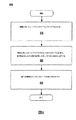
図1は、マイクロプロセッサを動作させるための従来技術による例示的動作周波数対供給電圧曲線110を示したものである。曲線110は、所望の動作周波数を達成するために必要な供給電圧Vddを示しており、たとえば周波数120で動作させるためには、供給電圧160が必要である。
FIG. 1 shows an exemplary operating frequency versus
曲線110は、たとえば多数のマイクロプロセッササンプルに対する周波数対電圧情報を収集することによって、マイクロプロセッサの母集団のための標準として確立することができる。良く知られている様々な統計的分析手法を使用して曲線110を確立し、性能とプロセス歩留りとの最適トレードオフを達成することができる。たとえば、全母集団の90%が曲線110より良好な周波数−電圧性能を示すように曲線110を確立することができる。曲線110を使用して1組の周波数−電圧動作点を確立することができる。たとえば周波数150は電圧190と対であり、周波数140は電圧180と、周波数130は電圧170と、また、周波数120は電圧160とそれぞれ対である。また、このような1組の周波数−電圧対(すなわち動作点)は、次の表1に示すように、テーブルの形態で表すことも可能である。

このようなプロセッサは、周波数および電圧の多数の異なる組合せ、すなわち動作点で動作するように構成される。専用の電力管理ソフトウェアによってプロセッサがモニタされ、プロセッサによる動的電力の消費を有利に最少化するために、これらの動作点と動作点の間で、ランタイム条件変更として動的にスイッチされる。 Such processors are configured to operate at a number of different combinations of frequencies and voltages, i.e. operating points. The processor is monitored by dedicated power management software and is dynamically switched between these operating points as runtime condition changes to advantageously minimize dynamic power consumption by the processor.
残念なことには、従来技術の場合、このような電力管理ソフトウェアは、1組の周波数−電圧動作点での動作に限定されている。たとえば特定の製造プロセスに対する特定のプロセッサモデルを認定試験している間に、1組の周波数−電圧動作点が決定され、そのプロセッサモデルのすべてのデバイスの動作に使用される。このような1組の周波数−電圧動作点は、プロセッサデバイスの母集団の最悪動作に基づいて決定され、たとえばそのプロセッサデバイスの汎用可用性に先立って決定される。 Unfortunately, in the prior art, such power management software is limited to operation at a set of frequency-voltage operating points. For example, while qualifying a particular processor model for a particular manufacturing process, a set of frequency-voltage operating points is determined and used to operate all devices of that processor model. Such a set of frequency-voltage operating points is determined based on the worst operation of the population of processor devices, eg, prior to general availability of the processor device.
プロセッサ集積回路(「マイクロプロセッサ」)の電力消費に関連する多くの特性は、製造プロセスの間に大きく変化する。たとえば、最大動作周波数、閾値電圧およびキャパシタンスは、バッチ間で、更には同じウェハにおいて、それぞれ30%以上変化することがある。漏れ電流は閾値電圧の指数であり、公称値から500%変化することがある。残念な結果として、このような1組の周波数−電圧動作点は、たとえば認定プロセスの間に、一般的にはプロセッサデバイスの汎用可用性に先立って決定されるプロセッサデバイスの母集団の最悪動作に基づいている。 Many characteristics associated with the power consumption of processor integrated circuits (“microprocessors”) vary greatly during the manufacturing process. For example, the maximum operating frequency, threshold voltage, and capacitance can vary by more than 30% between batches and even on the same wafer. Leakage current is an index of the threshold voltage and can vary from nominal by 500%. Unfortunately, such a set of frequency-voltage operating points is based on, for example, the worst behavior of the processor device population determined during the qualification process, generally prior to the general availability of the processor device. ing.
多くのプロセッサ、典型的には製造済み母集団の大半は、最悪性能に基づく1組の標準より多い有利な周波数−電圧動作点で動作させることができる。たとえば、標準組が1.2ボルトで600MHzの動作を指定している場合、個々のプロセッサデバイスの多くは、600MHzでたったの1.1ボルトで動作させることができる。しかしながら、このようなより良好な性能を発揮するプロセッサは、標準の周波数−電圧動作点での動作に不利益に設定されており、電力を無駄に消費している。また、このような部品は、通常、より低い閾値電圧を有することになり、より高い供給電圧での動作を強制されると、漏れ電流が増加することになる。これらの両方の効果が電力を過度に消費し、電池の寿命を、いたずらに、このような特定のプロセッサデバイスに対する最適な電池寿命より短くしている。 Many processors, typically the majority of the manufactured population, can be operated at advantageous frequency-voltage operating points over a set of standards based on worst performance. For example, if the standard set specifies 600 MHz operation at 1.2 volts, many of the individual processor devices can be operated at only 1.1 volts at 600 MHz. However, such a processor that exhibits better performance is disadvantageously set for operation at the standard frequency-voltage operating point and wastes power. Also, such components typically will have a lower threshold voltage, and leakage current will increase if they are forced to operate at a higher supply voltage. Both of these effects consume excessive power and unnecessarily reduce battery life below the optimum battery life for such a particular processor device.
また、通常、プロセッサモデルの商用寿命の間に、様々な洗練および改善がその製造プロセスに加えられる。これらの洗練および改善の中には、たとえば、既存の標準周波数−電圧動作点の組を最適ではない組にしているプロセッサ母集団の電力特性を改善するものもある。 Also, various refinements and improvements are typically added to the manufacturing process during the commercial life of the processor model. Some of these refinements and improvements, for example, improve the power characteristics of a processor population that makes existing standard frequency-voltage operating point pairs less than optimal.
従来技術は、主としてマイクロプロセッサの動的電力消費の低減に的を絞っているが、残念なことには、近代の半導体プロセス、たとえば最小フィーチャサイズが約0.13ミクロン以下のプロセスにおいては、総電力消費に占める静的電力消費を無視することはもはやできない。このようなプロセスの場合、静的電力は、総電力消費の1/2を占めることもある。また、静的電力が総電力に占める割合は、半導体プロセスの逐次生成に伴って増加する傾向がある。 Although the prior art focuses primarily on reducing the dynamic power consumption of microprocessors, unfortunately, in modern semiconductor processes, such as processes with minimum feature sizes of about 0.13 microns or less, Static power consumption in power consumption can no longer be ignored. For such a process, static power may account for 1/2 of the total power consumption. Further, the ratio of static power to the total power tends to increase with the sequential generation of semiconductor processes.
たとえば、最大動作周波数は、通常、量(1−Vt/Vdd)、つまり、供給電圧で除した閾値電圧を1から引いた量に比例している(微小プロセス幾何学の場合)。プロセス幾何学が縮小されると、通常、酸化膜の破壊などの有害な影響を回避するために供給電圧(Vdd)も低減される。したがって、有利な最大動作周波数を維持し、あるいは高くするためには、同じく閾値電圧を低くしなければならず、したがって、ゲート酸化膜は、ゲートがチャネルの制御を維持することができるよう、より薄く構築されている。ゲート酸化膜をより薄くすることにより、ゲートキャパシタンスを大きくすることができる。「オフ」であるか、あるいはCMOSデバイスの漏れ電流が一般的にゲートキャパシタンスに比例しているため、ゲート酸化膜をより薄くする傾向には、漏れ電流を大きくする傾向がある。残念なことには、漏れ電流が増加すると、静的電力の消費が著しく増加する。また、残念な結果として、半導体プロセスのサイズの絶えることのない縮小により、総電力消費に対する静的電力散逸の関与がこれまで以上に増加している。 For example, the maximum operating frequency is usually proportional to the quantity (1-Vt / Vdd), ie, the threshold voltage divided by the supply voltage minus one (for microprocess geometry). As the process geometry is reduced, the supply voltage (Vdd) is also typically reduced to avoid deleterious effects such as oxide breakdown. Thus, in order to maintain or increase the advantageous maximum operating frequency, the threshold voltage must also be lowered, so the gate oxide is more capable of maintaining the gate in control of the channel. It is built thinly. By making the gate oxide film thinner, the gate capacitance can be increased. Since the leakage current of a CMOS device is generally proportional to the gate capacitance, it tends to increase the leakage current in order to make the gate oxide thinner. Unfortunately, static current consumption increases significantly as leakage current increases. Also, unfortunately, the ever-increasing size of semiconductor processes has increased the contribution of static power dissipation to total power consumption.
また、漏れ電流は、デバイス幾何学の多数のアスペクトおよびインプラント特性の影響を受けるため、静的電力は、公称レベルの上下に500%も変化することがある。電力消費の面における性能は、移動プロセッサの重要な属性であるため、プロセッサの製造者は、通常、部品が最大電力レベルにおける特定のクロック速度、たとえば8.5ワットにおける1GHzに合致していることを試験し、認証している。周波数−電圧動作点の固定組で動作させる場合、このような最大電力レベルは、周波数−電圧動作点のその組によって指定される電圧で達成しなければならない。 Also, since the leakage current is affected by a number of aspects of device geometry and implant characteristics, static power can vary as much as 500% above and below the nominal level. Because performance in terms of power consumption is an important attribute of mobile processors, processor manufacturers typically require that components meet a specific clock speed at the maximum power level, for example 1 GHz at 8.5 watts. Has been tested and certified. When operating with a fixed set of frequency-voltage operating points, such maximum power level must be achieved at the voltage specified by that set of frequency-voltage operating points.
特定のプロセッサデバイスが標準周波数−電圧動作点における最大電力制限に合致することができない場合、そのプロセッサデバイスは除外されるか、あるいはより大きい電力の範疇、つまり製造試験におけるそれほど望ましくないカテゴリすなわち「貯蔵所」に置かれることになる。このような部品は、製造者に対する歩留り損失および潜在的な収入の損失を表しているが、このような部品は、要求されるクロック速度仕様および電力消費仕様の両方を、より低い電圧で達成することができることがしばしばである。 If a particular processor device fails to meet the maximum power limit at the standard frequency-voltage operating point, the processor device is excluded or has a higher power category, ie, a less desirable category or “storage” in manufacturing test. It will be placed in the place. While such components represent a yield loss and potential revenue loss to the manufacturer, such components achieve both the required clock speed specifications and power consumption specifications at lower voltages. Often it can be done.
したがって、従来技術による周波数−電圧動作点を制御するシステムおよび技法は、プロセッサの電力消費の低減に改善をもたらしているが、プロセッサの可変母集団のすべてに標準の動作点の組を使用しているため、電力の消費が最適ではなく、また、極めて望ましくない製造歩留り損失をもたらしている。 Thus, while prior art systems and techniques for controlling frequency-voltage operating points have provided improvements in reducing processor power consumption, using a standard operating point set for all of the variable population of processors. As such, power consumption is not optimal and results in highly undesirable manufacturing yield loss.
したがって、特定の集積回路の特性を反映している、集積回路のパッケージ後の特性表示に基づいて電力を適応制御するシステムおよび方法が必要である。 Accordingly, there is a need for a system and method for adaptively controlling power based on a post-package characteristic display of an integrated circuit that reflects the characteristics of the particular integrated circuit.
本発明すなわち集積回路のパッケージ後の特性表示に基づく適応電力制御についての以下の詳細説明では、本発明を完全に理解するために、多数の特定の詳細が示されている。しかしながら、当業者には、これらの特定の詳細がなくても本発明を実践することができ、あるいはこれらの特定の詳細の均等物を使用して本発明を実践することができることは認識されよう。したがって、本発明の態様を明確にするために、良く知られている方法、処理手順、コンポーネントおよび回路についての詳細な説明は、ここでは省略されている。 In the following detailed description of the present invention, ie, adaptive power control based on post-package characterization of an integrated circuit, numerous specific details are set forth in order to provide a thorough understanding of the present invention. However, those skilled in the art will recognize that the invention may be practiced without these specific details, or that equivalents of these specific details may be used to practice the invention. . Accordingly, detailed descriptions of well-known methods, procedures, components, and circuits are omitted herein for the sake of clarity.
表記法および名称集
以下の詳細説明のいくつかの部分(たとえばプロセス600、700、800、900、1000、1100、1200および1300)は、処理手順、ステップ、論理ブロック、処理、およびコンピュータメモリ上で実行することができるデータビットに対する動作の他の記号表現の形で示されている。これらの記述および表現は、データ処理分野の技術者に使用されている、それらの働きの本質を他の当業者に最も効果的に伝えるための手段である。処理手順、コンピュータ実行ステップ、論理ブロック、プロセス等は、ここでは一般的に、所望の結果を得るための自己無矛盾ステップシーケンスあるいは命令もしくはファームウェアと見なすべきである。ステップは、物理量の物理的な操作を必要とするステップである。通常、物理量は、必ずしもそうとは限らないが、記憶し、転送し、結合し、比較し、あるいはコンピュータシステムの中で操作することができる電気信号もしくは磁気信号の形態を取っている。これらの信号は、主として共通に利用するという理由で、ビット、値、エレメント、記号、特性、用語、数などとして参照することがしばしば便利であることが分かっている。
Notation and Naming Some parts of the following detailed description (eg, processes 600, 700, 800, 900, 1000, 1100, 1200 and 1300) are performed on processing procedures, steps, logic blocks, processing, and computer memory. Other symbolic representations of operations on data bits that can be performed are shown. These descriptions and representations are the means most effectively used by those skilled in the data processing arts to convey the nature of their work to others skilled in the art. Procedures, computer-executed steps, logic blocks, processes, etc. should generally be considered here as self-consistent step sequences or instructions or firmware to obtain the desired result. A step is a step that requires physical manipulation of physical quantities. Usually, a physical quantity is not necessarily so, but in the form of an electrical or magnetic signal that can be stored, transferred, combined, compared, or manipulated within a computer system. It has proven convenient at times, principally for reasons of common usage, to refer to these signals as bits, values, elements, symbols, characteristics, terms, numbers, or the like.
しかしながら、これらのすべての用語およびすべての類似用語は、適切な物理量に関連させるべきであり、また、これらの物理量に適用された単に便利なラベルに過ぎないことに留意されたい。以下の考察から明らかであるように、特に言及されていない限り、本発明を通して、「入手する」、「索引付けする」、「処理する」、「計算する」、「翻訳する」、「計算する」、「決定する」、「選択する」、「記憶する」、「認識する」、「生成する」、「選択する」、「移動させる」、「符号化する」、「結合する」、「試験する」、「設定する」、「動作させる」、「変換する」、「決定する」、「最適化する」、「合成する」、「グループ化する」、「予測する」、「記述する」、「測定する」、「記録する」、「関連付ける」などの用語を利用した考察は、コンピュータシステムのレジスタおよびメモリ内の物理(電子)量として表されたデータを、コンピュータシステムメモリあるいはレジスタもしくは他のこのような情報記憶装置、転送デバイスもしくは表示デバイス内の物理量として同様に表された他のデータに操作し、かつ、変換するコンピュータシステムもしくは類似の電子計算デバイスのアクションおよびプロセスを意味していることを理解されたい。 However, it should be noted that all these terms and all similar terms should be associated with the appropriate physical quantities and are merely convenient labels applied to these physical quantities. As will be apparent from the following discussion, unless otherwise stated, throughout the present invention, "obtain", "index", "process", "calculate", "translate", "calculate" ”,“ Determine ”,“ Select ”,“ Remember ”,“ Recognize ”,“ Generate ”,“ Select ”,“ Move ”,“ Encode ”,“ Combine ”,“ Test ” , "Set", "activate", "convert", "decide", "optimize", "synthesize", "group", "predict", "describe", Considerations using terms such as “measuring”, “recording”, “associating”, etc., represent the data represented as physical (electronic) quantities in the computer system registers and memory, computer system memory or registers or other Such information It should be understood to mean the actions and processes of a computer system or similar electronic computing device that manipulates and transforms other data that is also represented as physical quantities in memory, transfer devices or display devices. .
集積回路のパッケージ後の特性表示に基づく適応電力制御
本発明の実施形態について、高度に集積化された半導体の設計および動作のコンテキストの中で説明する。より詳細には、本発明の実施形態は、マイクロプロセッサの適応電力管理に関している。しかしながら、本発明のエレメントは、半導体動作の他の領域に利用することが可能であることを理解されたい。
Adaptive Power Control Based on Post-Packaging Characteristic Display of Integrated Circuits Embodiments of the invention are described in the context of the design and operation of highly integrated semiconductors. More specifically, embodiments of the invention relate to microprocessor adaptive power management. However, it should be understood that the elements of the present invention can be utilized in other areas of semiconductor operation.
2000年1月18日出願の、S.Halepeteらに対する「Adaptive Power Control」という名称の米国特許出願第09/484,516号は、参照によりその全体が本明細書に組み込まれている。 Filed on Jan. 18, 2000. US patent application Ser. No. 09 / 484,516 entitled “Adaptive Power Control” to Halepete et al. Is hereby incorporated by reference in its entirety.
半導体製造プロセスは、一般に高度な自己無矛盾プロセスであると見なされている。つまり、半導体製造プロセスは、集積回路設計の「厳密な」コピーの製造に極めて良好であり、ディジタル領域で動作する半導体製品の場合、とりわけ良好である。機能的には、半導体技術は、同様に機能する本質的に完璧なコピーの製造に成功している。 Semiconductor manufacturing processes are generally regarded as highly self-consistent processes. That is, the semiconductor manufacturing process is very good for producing “exact” copies of integrated circuit designs, especially for semiconductor products operating in the digital domain. Functionally, semiconductor technology has been successful in producing essentially perfect copies that function similarly.
しかしながら、半導体の多くのアナログ特性は極めて変化しやすく、たとえば閾値電圧、キャパシタンス、ゲート遅延、電流消費、最小動作電圧および最大動作周波数は、チップ間で30%以上変化することがある。漏れ電流すなわち「オフ」電流は、更に変化しやすく、たとえば公称レベルの上下500%の漏れ電流の変化は希なことではない。より詳細には、集積回路の電力消費に関連するパラメータは、極めて変化しやすい。 However, many analog characteristics of semiconductors are highly variable, for example threshold voltage, capacitance, gate delay, current consumption, minimum operating voltage and maximum operating frequency can vary by more than 30% from chip to chip. Leakage current or “off” current is more variable, for example, a change in leakage current of 500% above and below the nominal level is not uncommon. More particularly, parameters related to the power consumption of an integrated circuit are highly variable.
図2は、本発明の一実施形態による、特定の集積回路の例示的周波数−電圧特性を示したものである。曲線210は、測定した周波数−電圧特性を示したもので、製造済み母集団の特定の集積回路の出力に対応している。また、参考として、標準の周波数−電圧曲線110が示されている。曲線210で示す周波数−電圧特性は、標準曲線110とは異なっており、製造プロセスの結果が変動していることを反映していることを理解されたい。
FIG. 2 illustrates exemplary frequency-voltage characteristics of a particular integrated circuit, according to one embodiment of the present invention.
曲線210は、標準曲線110より良好な周波数−電圧特性を備えた特定の集積回路を示している。たとえば、曲線210で示す集積回路は、標準の周波数−電圧特性によって指定される供給電圧190(表1)より低い供給電圧260で周波数150を達成することができる。有利な結果として、このような集積回路は、標準の電圧(たとえば電圧190)での動作と比較して、より低い電圧(たとえば電圧260)延いてはより小さい電力で同じレベルの処理性能(周波数で表される)を提供することができる。
曲線210は、標準曲線(110)より有利な周波数−電圧特性を備えた集積回路を示している。通常、製造母集団の大半は、標準曲線を決定する際に、製造プロセスの歩留りを少なくとも部分的に最小化するために優れた周波数−電圧特性を有することになるが、このような標準周波数−電圧特性の有害な影響は、集積回路のほとんどが、それらの定格より良好な電力性能が可能であることである。
電力消費の面における性能は、移動プロセッサの重要な属性であるため、プロセッサの製造者は、通常、部品が最大電力レベルにおける特定のクロック速度に合致していることを試験し、認証している。周波数−電圧動作点の固定組で動作させる場合、このような最大電力レベルは、所望の周波数に対応する、周波数−電圧動作点のその組によって指定される電圧で達成しなければならない。たとえば、集積回路の電力レベルは、供給電圧190における周波数150に対する最大制限未満でなければならない。
Because performance in terms of power consumption is an important attribute of mobile processors, processor manufacturers typically test and certify that parts meet a specific clock speed at the maximum power level. . When operating with a fixed set of frequency-voltage operating points, such maximum power level must be achieved at the voltage specified by that set of frequency-voltage operating points, corresponding to the desired frequency. For example, the power level of the integrated circuit must be below the maximum limit for
たとえば曲線210に対応する集積回路のような「高速」部品は、「より速度の遅い」部品と比較すると、より低い電圧でより高い動作周波数を達成することができる。高速部品は、通常、より速度の遅い部品と比較すると、所与の電圧における電流消費も多く、したがって、曲線210に対応する集積回路は、供給電圧190、周波数150で容易に動作させることができるが、この集積回路は、通常、より多くの電流を消費するため、試験電圧における電力制限を超過することがある。従来技術の場合、曲線210に対応する集積回路は、所望の動作周波数、たとえば標準の周波数−電圧特性によって指定される電圧より低い電圧で周波数150を達成することは可能であるが、有害なことには消費する電力が多すぎるため、除外されることになる。
For example, a “fast” component, such as an integrated circuit corresponding to
典型的な動作周波数、たとえば数百メガヘルツからギガヘルツの範囲における集積回路の試験、たとえば曲線210の作成に必要な試験は、通常、集積回路がパッケージされた後に実行される。パッケージ部品の試験に必要な試験設備は、通常、ベアダイレベルもしくはウェハレベルの試験に必要な試験設備より安価である。また、たとえばリードフレームを含むパッケージングにより、パッケージデバイスの性能、とりわけ周波数性能に影響する多くの追加電気特性および熱特性が導入される。
Tests of integrated circuits at typical operating frequencies, such as in the range of several hundred megahertz to gigahertz, such as those required to create
残念なことには、パッケージングプロセスは、パッケージング材料、プロセス設備の運転経費および能力の点で高価である。パッケージ後におけるパッケージ半導体が望ましくない電力特性を有していることが分かると、パッケージングの経費が損失する。また、半導体のある種の不揮発性エレメント、たとえばデータ記憶ヒューズは、通常、パッケージングに先立ってのみセットすることができる。たとえば、データ記憶ヒューズは、直接アクセスされる(たとえばレーザによって)半導体構造にすることができ、あるいは一般的にはボンディングされないパッドを介してアクセスされる半導体構造にすることができる。これらおよびその他の理由により、集積回路の電力性能をパッケージングに先立って決定することがしばしば有利である。 Unfortunately, the packaging process is expensive in terms of packaging materials, process equipment operating costs and capabilities. If the packaged semiconductor after packaging is found to have undesirable power characteristics, packaging costs are lost. Also, certain non-volatile elements of semiconductors, such as data storage fuses, can usually only be set prior to packaging. For example, the data storage fuse can be a semiconductor structure that is directly accessed (eg, by a laser) or a semiconductor structure that is typically accessed through an unbonded pad. For these and other reasons, it is often advantageous to determine the power performance of an integrated circuit prior to packaging.
CMOS回路によって消費される電力は、静的部分と動的部分との2つの構成要素からなっている。動的電力は、近似的に、p=CV2fで与えられる。Cはアクティブスイッチングキャパシタンス、Vは供給電圧、fは動作周波数である。静的電力は、アイドル電流×電圧で表される。既に説明したように、通常、パッケージングに先立って集積回路を周波数で正確に試験することは不可能である。したがって動的電力を集積回路のパッケージングに先立って正確に測定することはできないが、キャパシタンスCおよびアイドル電流は、パッケージングによる影響が比較的小さく、また、ベアダイレベルおよび/またはウェハレベルで正確に測定することができる。 The power consumed by the CMOS circuit consists of two components: a static part and a dynamic part. The dynamic power is approximately given by p = CV 2 f. C is the active switching capacitance, V is the supply voltage, and f is the operating frequency. Static power is expressed as idle current × voltage. As already explained, it is usually not possible to accurately test an integrated circuit at frequency prior to packaging. Thus, although dynamic power cannot be accurately measured prior to integrated circuit packaging, capacitance C and idle current are relatively insensitive to packaging and are accurate at bare die level and / or wafer level. Can be measured.
本発明の一実施形態によれば、有利には、キャパシタンスが与えられると、パッケージングに先立って、仮想動作周波数に基づいて動的電力を予測することができる。たとえば、測定したキャパシタンスの値に基づいて、所望の動作周波数に対する動的電力を予測することができる。動作電圧は、たとえば標準の周波数−電圧動作点毎に指定することができる。また、パッケージが施されていないデバイス上でアイドル電流を測定することができるため、総電力(所望の動作周波数における)を直接予測することができる。 According to one embodiment of the present invention, advantageously, given the capacitance, dynamic power can be predicted based on the virtual operating frequency prior to packaging. For example, dynamic power for a desired operating frequency can be predicted based on the measured capacitance value. The operating voltage can be specified for each standard frequency-voltage operating point, for example. Also, the idle current can be measured on an unpackaged device, so the total power (at the desired operating frequency) can be predicted directly.
本発明の一実施形態によれば、電力消費のこのような予測(所望の動作周波数に対する)を使用して、パッケージングに先立って、過剰電力消費に基づいて除外された部品を試験することができる。しかしながら、既に説明したように、このような基準に基づく除外は、集積回路デバイス、たとえば図2に示す曲線210に対応する集積回路を有害に除外することになる。
According to one embodiment of the present invention, such an estimate of power consumption (relative to the desired operating frequency) can be used to test for excluded parts based on excess power consumption prior to packaging. it can. However, as already described, exclusion based on such criteria would detrimentally exclude integrated circuit devices, such as the integrated circuit corresponding to
本発明の代替実施形態によれば、所望の動作周波数の達成が可能であることを仮定して、最大電力制限を達成するために必要な最大電圧を決定することがより望ましい。たとえば、前述の電力予測では、電力(最大制限として)を指定して電圧の解を求めている。得られた電圧は、許容可能な電力レベルを達成するための所望の周波数で集積回路デバイスを動作させることができる最大電圧である。集積回路は、所望の周波数では試験されていないことを理解されたい。しかしながら、電力制限に合致するためには、集積回路は、得られた決定電圧に等しいか、あるいはそれより低い電圧の所望の周波数で動作しなければならない。 According to an alternative embodiment of the present invention, it is more desirable to determine the maximum voltage required to achieve the maximum power limit, assuming that the desired operating frequency can be achieved. For example, in the power prediction described above, power (as a maximum limit) is specified to find a voltage solution. The resulting voltage is the maximum voltage that can operate the integrated circuit device at the desired frequency to achieve an acceptable power level. It should be understood that the integrated circuit has not been tested at the desired frequency. However, in order to meet the power limit, the integrated circuit must operate at the desired frequency equal to or less than the resulting determined voltage.
本発明の一実施形態によれば、得られたこのような電圧の表現を符号化し、たとえば、集積回路のデータ記憶ヒューズ(たとえばリセット不能半導体フィーチャ)、電気的消去可能プログラマブルリードオンリメモリ(EEPROM)などの不揮発性エレメントの中にプログラムすることができる。たとえば、許容される最大電圧を集積回路の中に符号化することができる。別法としては、可変周波数−電圧特性の組へのマッピングを符号化することも可能である。 According to one embodiment of the present invention, the resulting representation of such a voltage is encoded, for example, an integrated circuit data storage fuse (eg, a non-resettable semiconductor feature), an electrically erasable programmable read only memory (EEPROM). Can be programmed into a non-volatile element. For example, the maximum voltage allowed can be encoded into the integrated circuit. Alternatively, the mapping to variable frequency-voltage characteristic pairs can be encoded.
もう一度図2を参照すると、本発明の一実施形態によれば、曲線220は、製造母集団の部分と部分の間の分割線を表している。集積回路の中には、たとえば曲線210に対応する集積回路のように曲線220の「左側」までの電圧−周波数特性を有している集積回路があり、また、曲線220と曲線110の間の電圧−周波数特性を有している集積回路もある。
Referring once again to FIG. 2, according to one embodiment of the present invention,
所望の動作周波数に対する許容最大電圧(最大電力レベルを超過しないよう)の決定に基づいて、特定の集積回路を上記複数のグループのうちの1つに置くことができる。曲線220は、周波数−電圧動作点の第2の組になり得るため、曲線110および220で表される2組の周波数−電圧動作点を使用して、所与の特定の集積回路の特定の特性に基づいて、より最適な電力レベルで集積回路を動作させることができる。たとえば曲線210に対応する集積回路は、曲線220の周波数−電圧動作点で動作させることができるため、同じ集積回路を曲線110の標準周波数−電圧動作点で動作させた場合と比較して電力が節約される。符号化された不揮発性回路エレメントは、動作中に使用すべき周波数−電圧動作点の組を決定することができる。
Based on the determination of the maximum allowable voltage for a desired operating frequency (so as not to exceed the maximum power level), a particular integrated circuit can be placed in one of the plurality of groups. Since
次の表2は、本発明の一実施形態による周波数−電圧動作点の組の例示的な対を示したものである。 Table 2 below shows an exemplary pair of frequency-voltage operating point pairs according to one embodiment of the present invention.
表2は、2組の周波数−電圧動作点を示したもので、左側の2列は標準の組であり、右側の2列は「高速」部品のための組である。たとえば、「高速」周波数−電圧動作点の組が曲線220に対応している場合、曲線210に対応する集積回路は、表2の「高速」組中の周波数−電圧点で有利に動作させることができる。このような「高速」動作点に従って動作させた場合の「高速」集積回路の消費電力は、動作点の標準の組で動作させた場合より少ない。
Table 2 shows two sets of frequency-voltage operating points, with the two left columns being the standard set and the two right columns being the set for “fast” components. For example, if the “fast” frequency-voltage operating point set corresponds to
本発明の実施形態は、集積回路の周波数−電圧特性を表すための他の方法にも適しており、たとえば、周波数−電圧特性の多項式記述あるいは近似記述の係数として周波数−電圧特性を表すことができる。 Embodiments of the present invention are also suitable for other methods for representing frequency-voltage characteristics of integrated circuits, eg, representing frequency-voltage characteristics as a polynomial or approximate description coefficient of frequency-voltage characteristics. it can.
また、同様に、このような符号化不揮発回路エレメントを使用して、パッケージデバイスの動的電力試験の供給電圧を決定することができる。たとえば、曲線210に対応する集積回路などの高速部品は、曲線220に対応する所望の周波数に対して、より低い供給電圧で試験しなければならない。従来技術の場合、高速部品は、標準の周波数−電圧動作点、たとえば曲線110で動作する最大電力制限試験には合格しないが、曲線220に対応するより低い電圧で動作するこのような試験には、より高い割合のデバイスが合格する。有利な結果として、本発明の実施形態により、製造歩留りが有利に向上する。
Similarly, such an encoded non-volatile circuit element can be used to determine the supply voltage for a dynamic power test of a package device. For example, a high speed component such as an integrated circuit corresponding to
本発明の実施形態は、表2に示す2つのグループより多い複数のグループへの製造母集団のセグメント化に適していることを理解されたい。周波数−電圧特性のより多くの組を生成し、このような複数の組の識別に使用されるより多くのビットを特定の集積回路の各々の中に符号化することができる。 It should be understood that embodiments of the present invention are suitable for segmenting a manufacturing population into a plurality of groups greater than the two groups shown in Table 2. More sets of frequency-voltage characteristics can be generated, and more bits used to identify such multiple sets can be encoded into each particular integrated circuit.
ほとんどの半導体の速度すなわち動作周波数は、温度によって変化する。たとえば、所与の電圧においては、集積回路は、温度が低い方がより高速で動作する。必然的な結果として、集積回路は、通常、同じ所望の周波数で、より高い温度で動作させるためにより高い供給電圧を必要とする場合、より低い温度で、より低い供給電圧を使用して、所望の周波数で動作させることになる。 The speed or operating frequency of most semiconductors varies with temperature. For example, at a given voltage, integrated circuits operate faster at lower temperatures. As an inevitable result, an integrated circuit typically uses a lower supply voltage at a lower temperature if it requires a higher supply voltage to operate at the same desired frequency and at a higher temperature. It will be operated at the frequency.
本発明の一実施形態によれば、チップの温度を使用して、所望の動作周波数に対する最適動作電圧を選択することができる。次の表3は、本発明の一実施形態による、チップの温度を組み込んだ周波数−電圧動作点の例示的な組を示したものである。 According to one embodiment of the invention, the temperature of the chip can be used to select the optimum operating voltage for the desired operating frequency. Table 3 below illustrates an exemplary set of frequency-voltage operating points that incorporate the temperature of the chip, according to one embodiment of the present invention.
表3は、4組の周波数−電圧動作点を示したもので、第2列および第3列は2つの標準組であり、右側の2列は、「高速」部品のための2組である。これらの組は、チップの温度、たとえば「ホット」および「クール」に基づく2つの標準組および2つの高速組である。チップの温度が50℃以下であることが分かっている場合、集積回路は、「クーラ」すなわち表3の下の部分に示す周波数−電圧点で動作させることが有利である。このような「クール」動作点に従って動作させた場合の集積回路の消費電力は、動作点の標準組(たとえば表2に示す、温度が考慮されていない組)で動作させた場合より少ない。 Table 3 shows four sets of frequency-voltage operating points, with the second and third columns being two standard sets, and the two right-hand columns being two sets for “fast” parts. . These sets are two standard sets and two high speed sets based on chip temperature, eg, “hot” and “cool”. If the temperature of the chip is known to be 50 ° C. or less, it is advantageous to operate the integrated circuit at the “cooler” or frequency-voltage point shown in the lower part of Table 3. The power consumption of the integrated circuit when operating according to such a “cool” operating point is less than when operating with a standard set of operating points (for example, a set that does not take temperature into consideration, as shown in Table 2).
本発明の実施形態は、表3に示す2つの温度グループより多い複数のグループへの周波数−電圧特性の特性化に適していることを理解されたい。温度依存周波数−電圧特性のより多くの組を生成し、このような複数の組の識別に使用されるより多くのビットを特定の集積回路の各々の中に符号化することができる。 It should be understood that embodiments of the present invention are suitable for characterizing frequency-voltage characteristics into a plurality of groups greater than the two temperature groups shown in Table 3. More sets of temperature dependent frequency-voltage characteristics can be generated, and more bits used to identify such multiple sets can be encoded into each particular integrated circuit.
場合によっては、可変周波数−電圧特性の組へのマッピングを集積回路の中に符号化することが望ましいが、この符号化には限界も存在している。第1の限界は、実際に集積回路の中に符号化することができる情報の量に関係している。マイクロプロセッサは、通常、その不揮発性記憶装置の量が極端に制限されているか、あるいは不揮発性記憶装置を有していない。このようなオンチップ不揮発性記憶装置が不足している理由の1つは、回路のサイズに関係しており、たとえば不揮発性記憶装置の1ビットは、マイクロプロセッサ回路をより最適に使用するための貴重な回路面積を消費している。もう1つの理由は、半導体プロセスに関係しており、たとえば多くのタイプの集積回路不揮発性記憶装置には、標準のマイクロプロセッサ回路には不要な半導体マスクおよび処理ステップを追加する必要がある。このようなマスクおよび処理ステップは高価であり、また、製造プロセスの複雑性が増すため、コストが増加し、かつ、歩留りが悪くなる。これらの理由およびその他により、通常、マイクロプロセッサには、追加処理ステップを必要とする不揮発性記憶装置は含まれていない。 In some cases, it may be desirable to encode the mapping to variable frequency-voltage characteristic pairs into an integrated circuit, but there are limitations to this encoding. The first limit is related to the amount of information that can actually be encoded into the integrated circuit. Microprocessors typically have an extremely limited amount of non-volatile storage or do not have non-volatile storage. One of the reasons for the lack of such on-chip non-volatile storage is related to the size of the circuit, for example, one bit of non-volatile storage for more optimal use of the microprocessor circuit Consumes valuable circuit area. Another reason is related to semiconductor processes, for example, many types of integrated circuit non-volatile memory devices require the addition of semiconductor masks and processing steps that are not required for standard microprocessor circuits. Such masks and processing steps are expensive and increase the complexity of the manufacturing process, resulting in increased costs and poor yield. For these reasons and others, microprocessors typically do not include non-volatile storage that requires additional processing steps.
第2の限界には、ダイレベル/ウェハレベルの試験の容量および能力が含まれている。ダイレベルおよびウェハレベルのテスタは、パッケージテスタより高価であり、また、既に説明したように、通常、パッケージングによる電気的な影響のため、集積回路の周波数−電圧挙動を完全に特性化することはできない。したがって、場合によっては、パッケージング後の集積回路の周波数−電圧挙動を特性化することがより望ましい。 The second limit includes die level / wafer level test capacity and capability. Die-level and wafer-level testers are more expensive than package testers and, as already explained, typically fully characterize the frequency-voltage behavior of integrated circuits due to the electrical effects of packaging. I can't. Thus, in some cases, it is more desirable to characterize the frequency-voltage behavior of the integrated circuit after packaging.
本発明の実施形態は、可変周波数−電圧特性の組へのマッピングの、パッケージング後の集積回路の中への符号化に適していることを理解されたい。たとえば、オンチップ不揮発性記憶装置は、パッケージピンを介してアクセスすることができ、また、テスタは、このような記憶装置にマッピング情報を書き込むことができる。しかしながら、オンチップ不揮発性記憶装置は、パッケージング後には符号化することができない場合がしばしばである。また、場合によっては、所望する量の情報を符号化するために利用することができる十分なオンチップ不揮発性記憶装置が存在していない場合もあり、そのような場合は、1つまたは複数の周波数−電圧特性を特定の集積回路に結合するための代替手段を使用しなければならない。 It should be understood that embodiments of the present invention are suitable for encoding a mapping of variable frequency-voltage characteristic pairs into an integrated circuit after packaging. For example, on-chip non-volatile storage devices can be accessed via package pins, and testers can write mapping information to such storage devices. However, on-chip non-volatile storage often cannot be encoded after packaging. Also, in some cases, there may not be enough on-chip non-volatile storage that can be used to encode the desired amount of information, in which case one or more Alternative means must be used to couple the frequency-voltage characteristics to a specific integrated circuit.
本発明の一実施形態によれば、特定の集積回路の周波数−電圧特性もしくは周波数−電圧特性のマッピングを、その特定の集積回路と結合している不揮発性記憶装置の中に符号化することができる。このようなデバイスの実施例には、それらに限定されないが、電気的消去可能プログラマブルリードオンリメモリ(EEPROM)、バッテリバックアップランダムアクセスメモリ(RAM)、マスクROM、強磁性RAM、半導体パッケージ内のデータ記憶ヒューズ、集積回路の一部であるデータ記憶ヒューズ、配線接続(たとえば、ピンをVccおよび/または接地に結合することによる符号化)などがある。 According to one embodiment of the present invention, a frequency-voltage characteristic or frequency-voltage characteristic mapping of a particular integrated circuit may be encoded in a non-volatile storage device coupled to that particular integrated circuit. it can. Examples of such devices include, but are not limited to, electrically erasable programmable read only memory (EEPROM), battery backed random access memory (RAM), mask ROM, ferromagnetic RAM, data storage in a semiconductor package. There are fuses, data storage fuses that are part of an integrated circuit, wiring connections (eg, encoding by coupling pins to Vcc and / or ground), and the like.
不揮発性記憶装置を特定の集積回路に結合するための望ましい方法の1つは、その特定の集積回路のパッケージ内、たとえばマルチチップモジュール内に記憶装置を備えることである。 One desirable method for coupling a non-volatile storage device to a particular integrated circuit is to provide the storage device in the package of that particular integrated circuit, eg, a multichip module.
本発明の実施形態は、特定の集積回路の周波数−電圧特性もしくは周波数−電圧特性のマッピングをその特定の集積回路に結合する他の方法にも適している。ある方法によれば、複数の集積回路に対する複数の周波数−電圧特性のコンピュータ可読媒体中のデータベースが維持され、その集積回路の属性、たとえば固有通し番号を識別することによって、特定の集積回路の特定の周波数−電圧特性が参照される。 Embodiments of the present invention are also suitable for other methods of coupling a frequency-voltage characteristic or frequency-voltage characteristic mapping of a particular integrated circuit to that particular integrated circuit. According to a method, a database in a computer readable medium of a plurality of frequency-voltage characteristics for a plurality of integrated circuits is maintained and a particular integrated circuit specific is identified by identifying an attribute of the integrated circuit, eg, a unique serial number. Reference is made to frequency-voltage characteristics.
この特定の周波数−電圧特性は、広範囲に渡る様々な手段、たとえばインターネットダウンロードを使用して転送することができ、その集積回路を使用した製品の製造中および/または使用中における多くのポイントで参照することができる。たとえば、その集積回路がマイクロプロセッサであったと仮定すると、そのマイクロプロセッサを備えたコンピュータの製造者は、そのコンピュータをアセンブルし、電子的にそのマイクロプロセッサの通し番号を入手し、たとえばデータファイル内のその特定の周波数−電圧特性を入手して、そのコンピュータに対する固有のROMを構成することができる。したがって、このようなROMは、その特定のコンピュータの心臓部であるマイクロプロセッサの特定の周波数−電圧特性を反映している。 This particular frequency-voltage characteristic can be transferred using a wide variety of means, such as Internet download, and referenced at many points during the manufacture and / or use of products using the integrated circuit. can do. For example, assuming that the integrated circuit was a microprocessor, the manufacturer of the computer with the microprocessor assembled the computer and electronically obtained the serial number of the microprocessor, eg, in the data file Specific frequency-voltage characteristics can be obtained to configure a unique ROM for the computer. Thus, such a ROM reflects the particular frequency-voltage characteristics of the microprocessor that is the heart of that particular computer.
一般的には、情報をパッケージング操作の後に符号化することによって、より大量の記憶装置をパッケージングに先立つ符号化に利用することができる。たとえば、メモリ半導体は、通常、マイクロプロセッサに含まれている数ビットではなく、数百万ビットの情報を備えている。また、マイクロプロセッサ、たとえば試験マシンに結合することができる、良く知られている多くのタイプのコンピュータシステムは、本質的に無制限の記憶装置を有することができ、更には本質的に無制限の記憶装置に結合することができる。 In general, by encoding information after a packaging operation, a larger amount of storage can be used for encoding prior to packaging. For example, memory semiconductors typically contain millions of bits of information rather than the few bits contained in a microprocessor. Also, many well-known computer systems that can be coupled to a microprocessor, such as a test machine, can have an essentially unlimited storage device, and even an essentially unlimited storage device. Can be combined.
また、パッケージングの後は、集積回路を完全に特性化することができるため、一般的には、パッケージング後の特定の集積回路に特化された情報をより大量に符号化することが可能である。本発明の一実施形態によれば、特定の集積回路がパッケーシングされた後に、その集積回路の特定の周波数−電圧特性情報を符号化することができる。 Also, after packaging, the integrated circuit can be fully characterized, so in general it is possible to encode more information specific to a particular integrated circuit after packaging. It is. According to an embodiment of the present invention, after a specific integrated circuit is packaged, specific frequency-voltage characteristic information of the integrated circuit can be encoded.
このようなパッケージング後の符号化によって、様々なタイプの情報を記憶することができる。たとえば、集積回路は、同様の周波数−電圧特性を有する集積回路の複数のグループのうちのいずれか1つに属するものとして特性化することができる。符号化された情報は、このようなグループの中から、特定の集積回路を最も良好に記述しているグループを識別することができる。 Various types of information can be stored by such post-packaging encoding. For example, an integrated circuit can be characterized as belonging to any one of a plurality of groups of integrated circuits having similar frequency-voltage characteristics. The encoded information can identify the group that best describes a particular integrated circuit from such groups.
別法としては、特定の集積回路の周波数−電圧特性を符号化することも可能であり、たとえば曲線210(図2)の属性を符号化することができる。この方法によれば、特定の集積回路上で動作する電力管理ソフトウェアは、1組の周波数−電圧特性を利用することができる。有利には、このような1組の特性により、複数の組を記憶する場合と比較して記憶装置要求事項が緩和される。また、電力管理ソフトウェアを単純化することができ、かつ、より有効に動作させることができるため、1組の動作点の間接的な参照が減少する。 Alternatively, the frequency-voltage characteristics of a particular integrated circuit can be encoded, for example, the attributes of curve 210 (FIG. 2) can be encoded. According to this method, power management software operating on a particular integrated circuit can utilize a set of frequency-voltage characteristics. Advantageously, such a set of characteristics reduces storage requirements as compared to storing multiple sets. Also, the power management software can be simplified and operated more effectively, reducing indirect references to a set of operating points.
本発明の実施形態は、データリダクション技法を始めとする、良く知られている広範囲に渡る様々な曲線表現方法、たとえば集積回路の周波数−電圧曲線などの表現技法に適している。本発明の一実施形態によれば、座標点を含んだテーブルを使用して周波数−電圧特性が表される。代替実施形態によれば、周波数−電圧特性の多項式記述もしくは近似記述の係数として周波数−電圧特性を表すことができる。 Embodiments of the present invention are suitable for a wide variety of well-known curve representation methods, such as data reduction techniques, such as representation techniques such as integrated circuit frequency-voltage curves. According to an embodiment of the present invention, a frequency-voltage characteristic is represented using a table including coordinate points. According to an alternative embodiment, the frequency-voltage characteristic can be represented as a coefficient of a polynomial description or approximate description of the frequency-voltage characteristic.
次の表4は、本発明の一実施形態による、特定のマイクロプロセッサの周波数−電圧特性を示したものである。 Table 4 below shows the frequency-voltage characteristics of a particular microprocessor according to one embodiment of the present invention.
表4には、1組の電圧−周波数特性しか含まれていないことを理解されたい(温度毎に任意選択である)。 It should be understood that Table 4 includes only one set of voltage-frequency characteristics (optional for each temperature).
図3は、本発明の一実施形態による集積回路モジュール300を示したものである。モジュール300は、マイクロプロセッサ310および不揮発性記憶装置320を備えている。マイクロプロセッサ310および記憶装置320は、カップリング330によって結合されている。モジュール300は、広範囲に渡る様々なタイプの集積回路パッケージ、たとえば印刷回路基板上への直接もしくは間接実装用に設計されたパッケージに概ね準拠している。パッケージの実施例には、それらに限定されないが、ボールグリッドアレイ、ピングリッドアレイ、シンQFP、LCCなどがある。モジュール300は、複数の集積回路を含むことができるマルチチップモジュールであってもよい。一実施例では、プロセッサ310および記憶装置320は、個別の集積回路である。
FIG. 3 illustrates an
また、本発明の実施形態は、たとえばダイレクトチップアタッチ(DCA)を介して回路基板に直接取り付けられるマイクロプロセッサを備えたモジュールに適している。本発明の実施形態には必要ではないが、DCAによって実装される集積回路は、通常、実装後に塗布されるカプセル封止材すなわち「グロップトップ」を有している。モジュールのコンポーネントを物理的に近接させる要求事項は、前述の考察には意図されていない。 Also, the embodiments of the present invention are suitable for a module including a microprocessor that is directly attached to a circuit board through, for example, direct chip attachment (DCA). Although not required for embodiments of the present invention, integrated circuits implemented by DCA typically have an encapsulant or “grop top” applied after mounting. The requirement to physically bring the components of the module in close proximity is not intended for the foregoing discussion.
不揮発性記憶装置320は、広範囲に渡る様々なタイプの不揮発性記憶装置に適している。たとえば、記憶装置320は、それらに限定されないが、電気的消去可能プログラマブルリードオンリメモリ(EEPROM)、バッテリバックアップランダムアクセスメモリ(RAM)、マスクROM、強磁性RAMを始めとする集積回路デバイスであってもよい。また、記憶装置320は、半導体パッケージ内のデータ記憶ヒューズ、集積回路の一部であるデータ記憶ヒューズ、配線接続(たとえば、ピンをVccおよび/または接地に結合することによる符号化)などを始めとする、広範囲に渡る他の様々なタイプのデータ記憶装置に適している。 The non-volatile storage device 320 is suitable for various types of non-volatile storage devices. For example, the storage device 320 is an integrated circuit device including, but not limited to, an electrically erasable programmable read only memory (EEPROM), a battery backup random access memory (RAM), a mask ROM, and a ferromagnetic RAM. Also good. Storage device 320 also includes data storage fuses in semiconductor packages, data storage fuses that are part of integrated circuits, wiring connections (eg, encoding by coupling pins to Vcc and / or ground), and the like. It is suitable for a wide variety of other types of data storage devices.
図4は、本発明の一実施形態によるデバイス400を示したものである。デバイス400は、コンピュータもしくはコンピュータの一部、たとえばコンピュータマザーボードを形成することができる。デバイス400は、マイクロプロセッサ410およびメモリ空間450を備えている。マイクロプロセッサ410は、複数の電圧での動作が可能であり、更には複数の周波数での動作が可能である。
FIG. 4 shows a device 400 according to one embodiment of the present invention. Device 400 may form a computer or part of a computer, such as a computer motherboard. The device 400 includes a
メモリ空間450は、マイクロプロセッサ410に結合されている。メモリ空間450は、それらに限定されないが、マイクロプロセッサ410内の内部RAMもしくはROM、マイクロプロセッサ410の外部のRAMもしくはROM、およびコンピュータ可読媒体の他の形態を始めとする、良く知られている広範囲に渡る様々なタイプのメモリに適している。
Memory space 450 is coupled to
電圧源420は、マイクロプロセッサ410に結合されている。電圧源420は、選択可能な電圧430をマイクロプロセッサ410に供給している。マイクロプロセッサ410は、電圧源420に最適電圧を選択させるために、カップリング440を介して電圧源420に結合されている。
本発明の代替実施形態によれば、デバイス400は、更に、メモリ空間460を備えることができる。メモリ空間460は、たとえばメモリ空間450と同じ結合手段を介してマイクロプロセッサ410に結合されている。メモリ空間460は、メモリ空間450に関連して上で説明したメモリと同様のタイプのメモリに適しており、更に、メモリ空間450と同じ物理デバイス内への配置に適している。しかしながら、メモリ空間460は、必ずしもメモリ空間450と同じ物理デバイス内に配置する必要はなく、これらの2つのメモリのタイプおよび/またはデバイスを異なるタイプおよび/またはデバイスにすることによって、コンピュータ400をある程度最適化することが優先される。
According to an alternative embodiment of the present invention, the device 400 can further comprise a memory space 460. Memory space 460 is coupled to
本発明の他の代替実施形態によれば、デバイス400は、論理470を備えることができる。論理470は、メモリ460およびマイクロプロセッサ410に結合されている。論理470は、マイクロプロセッサ410によって決定することができる所望の動作周波数を入手し、また、メモリ460を使用して対応する電圧を決定している。論理470は、マイクロプロセッサ410を所望の動作周波数および対応する電圧で動作させている。論理470は、たとえばマイクロプロセッサ410上でのソフトウェア実施形態の実行に適している。また、論理470は、第2のプロセッサ(図示せず)上での動作が可能であり、あるいはゲートおよび/またはラッチの機能的な組を備えることも可能である。論理470は、マイクロプロセッサ410の内部もしくは外部への配置に適している。
According to other alternative embodiments of the present invention, device 400 can comprise logic 470. Logic 470 is coupled to memory 460 and
図5A、5Bおよび5Cは、計算エレメントの本発明の実施形態による構成を示したものである。図5Aには、計算エレメントの本発明の一実施形態による構成570が示されている。構成570は、広範囲に渡る様々な配置、実装および相互接続構造に適している。たとえば、構成570は、コンピュータ「マザーボード」の一部であってもよい。別法としては、構成570は、マルチチップモジュールであってもよい。
FIGS. 5A, 5B and 5C show the configuration of the computational element according to an embodiment of the invention. FIG. 5A shows a
データ構造505は、プロセッサ501に特化された電圧−周波数の関係の情報を備えている。従来技術とは対照的に、データ構造505の情報は、同様の設計のプロセッサの母集団に概ね関係する情報ではなく、プロセッサ501の試験に基づいている。データ構造505は、プロセッサ501の外部メモリであるメモリ506に常駐させることができる。メモリ506は、たとえばROM集積回路であってもよい。本発明の実施形態は、たとえばRAM、回転磁気記憶装置などの他のタイプのメモリにも適している。
The
制御論理507は、データ構造505からの情報を使用して、プロセッサ501の動作電圧および/または動作周波数を制御している。このような制御により、プロセッサ501が消費する電力を最少化することができる。制御論理507は、プロセッサ501上でのソフトウェアの実行に適している。
図5Bには、計算エレメントの本発明の一実施形態による構成580が示されている。構成580は、広範囲に渡る様々な配置、実装および相互接続構造に適している。たとえば、構成580は、コンピュータ「マザーボード」の一部であってもよい。別法としては、構成580は、マルチチップモジュールであってもよい。
FIG. 5B shows a
データ構造530は、プロセッサ503のタイプのプロセッサのクラスのための電圧−周波数の関係の情報を備えている。同様に、データ構造540および550も、それぞれプロセッサ503のタイプのプロセッサの他のクラスのための電圧−周波数の関係の情報を備えている。従来技術とは対照的に、データ構造530〜550の情報は、プロセッサ503と同じタイプのプロセッサの製造母集団のセグメントを表している。通常、情報530、540および550は異なっている。本発明の実施形態は、可変数のこのようなデータ構造に適している。データ構造530、540および550は、プロセッサ503の外部メモリであるメモリ560に常駐させることができる。メモリ560は、たとえばROM集積回路であってもよい。本発明の実施形態は、たとえばRAM、回転磁気記憶装置などの他のタイプのメモリにも適している。
クラス識別子520は、プロセッサ503に最も良好に対応する電圧−周波数の関係(たとえばデータ構造530、540もしくは550に含まれている)に関する情報を備えている。プロセッサ503の製造中にクラス識別子520が決定され、記録される。クラス識別子のこのような決定および記録は、プロセッサ503のパッケージングに先立って実行することができる。通常、クラス識別子520は数ビットであり、多くのタイプの不揮発性記憶装置、たとえばデータ記憶ヒューズもしくは電気的消去可能プログラマブルリードオンリメモリ(EEPROM)に適している。
Class identifier 520 comprises information regarding the voltage-frequency relationship that best corresponds to processor 503 (eg, included in
制御論理525は、クラス識別子520から情報を入手して、プロセッサ503に対応するデータ構造、たとえば530、540もしくは560を決定しており、また、プロセッサ503の動作電圧および/または動作周波数を制御するためにはこの情報を使用しなければならない。このような制御により、プロセッサ503が消費する電力を最少化することができる。制御論理525は、プロセッサ503上でのソフトウェアの実行に適している。
Control logic 525 obtains information from class identifier 520 to determine a data structure corresponding to
図5Cには、計算エレメントの本発明の一実施形態による構成590が示されている。構成590は、広範囲に渡る様々な配置、実装および相互接続構造に適している。たとえば、構成590は、コンピュータ「マザーボード」の一部であってもよい。別法としては、構成590は、マルチチップモジュールであってもよい。
FIG. 5C shows a
データ構造505は、プロセッサ502に特化された電圧−周波数の関係の情報を備えている。従来技術とは対照的に、データ構造505の情報は、同様の設計のプロセッサの母集団に概ね関係する情報ではなく、プロセッサ502の試験に基づいている。データ構造505は、プロセッサ502の内部に存在している。データ構造505は、プロセッサ内に含むことができる、良く知られている広範囲に渡る様々なタイプのメモリ、たとえば不揮発性RAM、電気的消去可能プログラマブルリードオンリメモリ(EEPROM)等に記憶することができる。
The
制御論理508は、データ構造505からの情報を使用して、プロセッサ502の動作電圧および/または動作周波数を制御している。このような制御により、プロセッサ502が消費する電力を最少化することができる。制御論理508は、プロセッサ502上でのソフトウェアの実行に適している。
Control logic 508 uses information from
図6は、本発明の一実施形態によるマイクロプロセッサ製造方法600を示したものである。ステップ610で、マイクロプロセッサに必要な、指定周波数における電力制限に合致するための電圧が決定される。この電圧は、たとえば、指定周波数でマイクロプロセッサを動作させ、その電力消費を測定することによって決定することができる。 FIG. 6 illustrates a microprocessor manufacturing method 600 according to one embodiment of the invention. At step 610, the voltage required to meet the power limit at the specified frequency required for the microprocessor is determined. This voltage can be determined, for example, by operating a microprocessor at a specified frequency and measuring its power consumption.
ステップ620で、その電圧の情報がコンピュータ可読媒体に記憶される。本発明の実施形態は、集積回路テスタもしくは製造データロギングシステムのメモリすなわち記憶システム、マイクロプロセッサの共通パッケージ内の集積回路、個別集積回路メモリなどを始めとする、広範囲に渡る様々なタイプのコンピュータ可読媒体での情報の記憶に適している。本発明の一実施形態によれば、この情報は、マイクロプロセッサに特化された周波数−電圧の関係を含んでいる。
At
図7は、本発明の一実施形態によるマイクロプロセッサ製造方法700を示したものである。ステップ710で、マイクロプロセッサに必要な、複数の指定周波数の各々で動作させるための最適電圧が決定され、電圧−周波数の複数の関係が生成される。この電圧−周波数の関係は、上記表4と同様である。
FIG. 7 illustrates a
ステップ720で、その複数の関係の情報がコンピュータ可読媒体に記憶される。本発明の実施形態は、集積回路テスタもしくは製造データロギングシステムのメモリすなわち記憶システム、マイクロプロセッサの共通パッケージ内の集積回路、個別集積回路メモリなどを始めとする、広範囲に渡る様々なタイプのコンピュータ可読媒体での情報の記憶に適している。
At
図8は、本発明の一実施形態によるマイクロプロセッサ製造方法800を示したものである。ステップ810で、複数の未パッケージマイクロプロセッサがアクセスされる。「パッケージング」などの用語は、出荷あるいは消費者パッケージングではなく、半導体パッケージング、たとえばピングリッドアレイパッケージを意味していることを理解されたい。マイクロプロセッサは、ウェハの形態であってもよい。
FIG. 8 illustrates a microprocessor manufacturing method 800 according to one embodiment of the invention. At
ステップ820で、複数の未パッケージマイクロプロセッサのうちの1つに必要な、指定周波数における電力制限に合致するための電圧が決定される。この電圧は、マイクロプロセッサのキャパシタンスおよび/またはアイドル電流を測定することによって決定することができる。 At step 820, the voltage required to meet the power limit at the specified frequency required for one of the plurality of unpackaged microprocessors is determined. This voltage can be determined by measuring the capacitance and / or idle current of the microprocessor.
ステップ830で、前記電圧の情報がマイクロプロセッサの中に符号化される。本発明の実施形態は、マイクロプロセッサの一部であってもよく、また、ステップ830で符号化することができる、良く知られている広範囲に渡る様々なタイプの記憶装置に適している。この記憶装置の実施例には、それらに限定されないが、データ記憶ヒューズ、電気的消去可能リードオンリメモリなどがある。 In step 830, the voltage information is encoded into the microprocessor. Embodiments of the present invention are suitable for a wide variety of well-known various types of storage devices that may be part of a microprocessor and that can be encoded at step 830. Examples of this storage device include, but are not limited to, a data storage fuse, an electrically erasable read only memory, and the like.
図9は、本発明の一実施形態による、集積回路を動作させる方法900を示したものである。ステップ910で、集積回路の周波数−電圧特性が測定され、記録される。集積回路は、マイクロプロセッサであってもよく、また、パッケージされていても、あるいはパッケージされていなくてもよい。
FIG. 9 illustrates a method 900 for operating an integrated circuit, according to one embodiment of the invention. At
ステップ920で、集積回路の動作を最適化するために、周波数−電圧特性が集積回路に結合される。周波数−電圧特性は、集積回路内の符号化情報もしくは集積回路と共に顧客に引き渡されるデバイス内の符号化情報を介した方法を始めとする、広範囲に渡る様々な方法で集積回路に結合することができる。本発明の代替実施形態によれば、この結合は、複数の集積回路の複数の周波数−電圧特性のコンピュータ可読媒体中のデータベースを維持する形態を取ることができる。この場合、特定の集積回路の特定の周波数−電圧特性は、その集積回路の属性、たとえば固有通し番号を識別することによって参照することができる。
At
ステップ930で、周波数−電圧特性によって指定される電圧および周波数で集積回路が動作する。
In
図10は、本発明の一実施形態による、マイクロプロセッサを動作させる方法1000を示したものである。ステップ1010で、マイクロプロセッサのための所望の動作周波数が決定される。有利な周波数を決定する典型的な手段の1つは、そのマイクロプロセッサ上で動作するソフトウェアの処理ニーズに基づいている。
FIG. 10 illustrates a
ステップ1020で、マイクロプロセッサを所望の動作周波数で動作させるための最適電圧が選択される。選択される最適電圧は、そのマイクロプロセッサに特化された特性に基づいている。
At
ステップ1030で、最適電圧でマイクロプロセッサが動作する。たとえば、マイクロプロセッサは、選択可能電圧源、たとえば図4に示す電圧源420に最適電圧を出力させることができる。本発明の代替実施形態によれば、最適電圧で動作している間、有利な周波数でマイクロプロセッサを動作させることができる。
In
図11は、本発明の一実施形態による、マイクロプロセッサを動作させる方法1100を示したものである。ステップ1120で、マイクロプロセッサを動作させる設定周波数が入手される。
FIG. 11 illustrates a
ステップ1130で、その設定周波数を使用して、その設定周波数に対応する、マイクロプロセッサがその設定周波数で最適動作する設定電圧が決定される。この決定は、マイクロプロセッサに特化された電圧−周波数の関係に基づいている。
In
ステップ1140で、その設定周波数および対応する設定電圧でマイクロプロセッサが動作する。
In
任意選択のステップ1110で、マイクロプロセッサが実行する同時動作の組を調査することによって設定周波数が決定される。
In
図12は、本発明の一実施形態による、マイクロプロセッサを特性化する方法1200を示したものである。ステップ1210で、マイクロプロセッサに特化された周波数−電圧の関係が測定され、記録される。この周波数−電圧の関係は、そのマイクロプロセッサを最適動作させるための周波数−電圧対を記録することができる。本発明の実施形態は、良く知られている様々なデータリダクション方法を始めとする、良く知られている他の関係記録方法に適している。
FIG. 12 illustrates a
ステップ1220で、マイクロプロセッサを最適使用するために、マイクロプロセッサを動作させている間、前記周波数−電圧の関係を入手し、かつ、使用することができるよう、周波数−電圧の関係がマイクロプロセッサに結合される。
In
図13は、本発明の一実施形態による、マイクロプロセッサを動作させる方法1300を示したものである。ステップ1310で、マイクロプロセッサのための所望の動作周波数が決定される。本発明の実施形態は、有利な周波数を決定するための様々な最適化に適している。有利な周波数を決定する典型的な手段の1つは、マイクロプロセッサ上で動作するソフトウェアの処理ニーズに基づいている。
FIG. 13 illustrates a
ステップ1320で、マイクロプロセッサに特化された情報が入手される。たとえば、この情報は、メモリ、たとえば図4に示すメモリ450に記憶することができ、この情報を使用して、有利な周波数でマイクロプロセッサを動作させるための最適電圧が決定される。この最適電圧は、マイクロプロセッサの特性に基づいている。
At
本発明の代替実施形態によれば、この情報は、マイクロプロセッサ内から入手することができる。 According to an alternative embodiment of the invention, this information can be obtained from within the microprocessor.
ステップ1330で、最適電圧でマイクロプロセッサが動作する。たとえば、マイクロプロセッサは、選択可能電圧源、たとえば図4に示す電圧源420に最適電圧を出力させることができる。本発明の代替実施形態によれば、最適電圧で動作している間、有利な周波数でマイクロプロセッサを動作させることができる。必要に応じてステップ1310から1330を繰り返すことができる。たとえば負荷の変化を処理する場合、有利な新しい動作周波数を決定し、かつ、新しい動作周波数に対応する電圧を入手することができ、その新しい周波数および電圧でマイクロプロセッサを動作させることができる。
In
集積回路の電力を適応制御するシステムおよび方法が開示される。集積回路のための所望の動作周波数が決定される。集積回路はマイクロプロセッサであってもよく、そのマイクロプロセッサの決定済み所望処理負荷に基づいて所望の動作周波数を決定することができる。マイクロプロセッサを所望の動作周波数で動作させるための最適電圧が選択される。この最適電圧の選択は、そのマイクロプロセッサに特化された特性に基づいており、マイクロプロセッサは、最適電圧で動作する。 Disclosed are systems and methods for adaptively controlling integrated circuit power. A desired operating frequency for the integrated circuit is determined. The integrated circuit may be a microprocessor, and a desired operating frequency can be determined based on the determined desired processing load of the microprocessor. The optimum voltage for operating the microprocessor at the desired operating frequency is selected. This selection of the optimum voltage is based on characteristics specific to the microprocessor, and the microprocessor operates at the optimum voltage.
本発明の実施形態により、集積回路が消費する電力をその集積回路の特定の特性に基づいて適応制御するための手段が提供される。また、本発明の実施形態により、既存のマイクロプロセッサプロセスおよび設備に、確立したツールおよび技法を改造することなく上記達成すべき解決法が提供される。 Embodiments of the present invention provide a means for adaptively controlling the power consumed by an integrated circuit based on specific characteristics of the integrated circuit. Embodiments of the present invention also provide a solution to be achieved by modifying existing microprocessor processes and equipment without modifying established tools and techniques.
以上、本発明の好ましい実施形態である、集積回路のパッケージ後の特性表示に基づく適応電力制御について説明した。本発明について、特定の実施形態を使用して説明したが、このような実施形態に限定されるものとして本発明を解釈してはならず、本発明は、特許請求の範囲に従って解釈すべきであることを理解されたい。 The adaptive power control based on the characteristic display after packaging of the integrated circuit, which is a preferred embodiment of the present invention, has been described above. Although the invention has been described using specific embodiments, the invention should not be construed as limited to such embodiments, and the invention should be construed according to the claims that follow. I want you to understand.
Claims (47)
前記マイクロプロセッサのための所望の動作周波数を決定するステップと、
前記マイクロプロセッサに特化された情報を入手するステップであって、前記情報は、前記所望の動作周波数で前記マイクロプロセッサを動作させるための最適電圧を決定するために使用され、前記最適電圧は、前記マイクロプロセッサの特性に基づいているところのステップと、
前記最適電圧で前記マイクロプロセッサを動作させるステップと
を含む方法。 A method of operating a microprocessor comprising:
Determining a desired operating frequency for the microprocessor;
Obtaining information specific to the microprocessor, wherein the information is used to determine an optimum voltage for operating the microprocessor at the desired operating frequency, the optimum voltage being: Steps based on the characteristics of the microprocessor;
Operating the microprocessor at the optimum voltage.
指定周波数における電力制限に合致するために、前記マイクロプロセッサに必要な電圧を決定するステップと、
前記電圧の情報をコンピュータ可読媒体に記憶するステップと
を含む方法。 A method of manufacturing a microprocessor, comprising:
Determining the voltage required for the microprocessor to meet power limits at a specified frequency;
Storing the voltage information on a computer readable medium.
複数の指定周波数の各々で動作させるために、前記マイクロプロセッサに必要な最適電圧を決定して、電圧−周波数の複数の関係を生成するステップと、
前記複数の関係の情報をコンピュータ可読媒体に記憶するステップと
を含む方法。 A method of manufacturing a microprocessor, comprising:
Determining an optimum voltage required for the microprocessor to operate at each of a plurality of specified frequencies and generating a plurality of voltage-frequency relationships;
Storing the plurality of relationship information on a computer readable medium.
前記マイクロプロセッサに結合された不揮発性記憶装置の少なくとも1つのビットとを備え、
前記不揮発性記憶装置が、前記マイクロプロセッサの周波数−電圧特性の情報を含む集積回路モジュール。 A microprocessor;
And at least one bit of non-volatile storage coupled to the microprocessor,
An integrated circuit module, wherein the nonvolatile memory device includes information on frequency-voltage characteristics of the microprocessor.
前記1組の周波数−電圧特性が、マイクロプロセッサが所望の周波数で動作するために必要な最低動作電圧を指定し、更に、
前記組の個々の周波数−電圧特性が、前記マイクロプロセッサに特化されている
ところのデータ構造。 A data structure in a computer readable memory with a set of frequency-voltage characteristics comprising:
The set of frequency-voltage characteristics specifies a minimum operating voltage required for the microprocessor to operate at a desired frequency;
A data structure in which the individual frequency-voltage characteristics of the set are specialized for the microprocessor.
前記マイクロプロセッサに結合され、前記マイクロプロセッサの集積回路に選択可能電圧を供給するための電圧源と、
前記マイクロプロセッサに結合され、前記マイクロプロセッサの動作電圧を最適化する方法を実施するための命令を含むメモリ空間と
を備えたコンピュータであって、前記方法が、
前記マイクロプロセッサのための所望の動作周波数を決定するステップと、
前記マイクロプロセッサに特化された情報を入手するステップであって、前記情報は、前記所望の動作周波数で前記マイクロプロセッサを動作させるための最適電圧を決定するために使用され、前記最適電圧は、前記マイクロプロセッサの特性に基づいているところのステップと、
前記電圧源に、前記最適電圧を前記マイクロプロセッサに供給させるステップとを含むコンピュータ。 A microprocessor;
A voltage source coupled to the microprocessor for supplying a selectable voltage to the integrated circuit of the microprocessor;
A computer coupled to the microprocessor and comprising a memory space including instructions for performing a method for optimizing the operating voltage of the microprocessor, the method comprising:
Determining a desired operating frequency for the microprocessor;
Obtaining information specific to the microprocessor, wherein the information is used to determine an optimum voltage for operating the microprocessor at the desired operating frequency, the optimum voltage being: Steps based on the characteristics of the microprocessor;
Causing the voltage source to supply the optimum voltage to the microprocessor.
前記1組の周波数−電圧特性が、マイクロプロセッサが所望の周波数で動作するために必要な最低動作電圧を指定し、更に、
前記組の個々の周波数−電圧特性が、前記マイクロプロセッサに特化されている、請求項36に記載のコンピュータ。 Further comprising a memory space including a set of frequency-voltage characteristics;
The set of frequency-voltage characteristics specifies a minimum operating voltage required for the microprocessor to operate at a desired frequency;
37. The computer of claim 36, wherein the set of individual frequency-voltage characteristics are specialized for the microprocessor.
前記マイクロプロセッサの温度を入手するステップと、
前記温度依存動作電圧情報を入手して、前記所望の動作周波数および前記マイクロプロセッサの前記温度で前記マイクロプロセッサを動作させるための最適電圧を決定するステップと
を更に含む、請求項41に記載のコンピュータ。 The method of optimizing the operating voltage of the microprocessor integrated circuit comprises:
Obtaining the temperature of the microprocessor;
42. The computer of claim 41, further comprising: obtaining the temperature dependent operating voltage information to determine an optimum voltage for operating the microprocessor at the desired operating frequency and the temperature of the microprocessor. .
特別に測定された前記マイクロプロセッサの電圧−周波数の関係を記憶するメモリであって、前記電圧−周波数の関係が電圧−周波数の複数の対からなり、各対が、関連する周波数に対する最適電圧を指示するところのメモリと、
前記メモリを使用して対応する電圧を決定し、更に、所望の動作周波数および前記対応する電圧で前記マイクロプロセッサを動作させるために、所望の動作周波数を入手するための論理と
を備えた電子デバイス。 A microprocessor capable of operating at multiple voltages, and further capable of operating at multiple frequencies;
A memory for storing a specially measured voltage-frequency relationship of the microprocessor, the voltage-frequency relationship comprising a plurality of voltage-frequency pairs, each pair having an optimum voltage for the associated frequency. The memory to point to,
An electronic device comprising: determining a corresponding voltage using the memory; and logic for obtaining a desired operating frequency to operate the microprocessor at the desired operating frequency and the corresponding voltage .
Applications Claiming Priority (2)
| Application Number | Priority Date | Filing Date | Title |
|---|---|---|---|
| US10/334,919 US7953990B2 (en) | 2002-12-31 | 2002-12-31 | Adaptive power control based on post package characterization of integrated circuits |
| PCT/US2003/041403 WO2004061634A2 (en) | 2002-12-31 | 2003-12-29 | Manufacture and operation of integrated circuit |
Related Child Applications (1)
| Application Number | Title | Priority Date | Filing Date |
|---|---|---|---|
| JP2009100766A Division JP2009217830A (en) | 2002-12-31 | 2009-04-17 | Microprocessor, integrated circuit module including microprocessor, electronic device, computer, method for operating and manufacturing microprocessor, and data structure for microprocessor |
Publications (2)
| Publication Number | Publication Date |
|---|---|
| JP2006512683A true JP2006512683A (en) | 2006-04-13 |
| JP2006512683A5 JP2006512683A5 (en) | 2007-02-15 |
Family
ID=32655205
Family Applications (2)
| Application Number | Title | Priority Date | Filing Date |
|---|---|---|---|
| JP2004565752A Pending JP2006512683A (en) | 2002-12-31 | 2003-12-29 | Integrated circuit manufacturing and operation |
| JP2009100766A Pending JP2009217830A (en) | 2002-12-31 | 2009-04-17 | Microprocessor, integrated circuit module including microprocessor, electronic device, computer, method for operating and manufacturing microprocessor, and data structure for microprocessor |
Family Applications After (1)
| Application Number | Title | Priority Date | Filing Date |
|---|---|---|---|
| JP2009100766A Pending JP2009217830A (en) | 2002-12-31 | 2009-04-17 | Microprocessor, integrated circuit module including microprocessor, electronic device, computer, method for operating and manufacturing microprocessor, and data structure for microprocessor |
Country Status (4)
| Country | Link |
|---|---|
| US (2) | US7953990B2 (en) |
| JP (2) | JP2006512683A (en) |
| AU (1) | AU2003300400A1 (en) |
| WO (1) | WO2004061634A2 (en) |
Cited By (1)
| Publication number | Priority date | Publication date | Assignee | Title |
|---|---|---|---|---|
| WO2008081916A1 (en) * | 2006-12-28 | 2008-07-10 | Nec Corporation | Semiconductor integrated circuit device and power supply voltage control system |
Families Citing this family (25)
| Publication number | Priority date | Publication date | Assignee | Title |
|---|---|---|---|---|
| US7698583B2 (en) * | 2002-10-03 | 2010-04-13 | Via Technologies, Inc. | Microprocessor capable of dynamically reducing its power consumption in response to varying operating temperature |
| US7814350B2 (en) * | 2002-10-03 | 2010-10-12 | Via Technologies, Inc. | Microprocessor with improved thermal monitoring and protection mechanism |
| US7953990B2 (en) * | 2002-12-31 | 2011-05-31 | Stewart Thomas E | Adaptive power control based on post package characterization of integrated circuits |
| US7228242B2 (en) * | 2002-12-31 | 2007-06-05 | Transmeta Corporation | Adaptive power control based on pre package characterization of integrated circuits |
| TW200416556A (en) * | 2003-02-25 | 2004-09-01 | Asustek Comp Inc | Portable computer carrying desktop computer processor and power saving method thereof |
| US7649402B1 (en) | 2003-12-23 | 2010-01-19 | Tien-Min Chen | Feedback-controlled body-bias voltage source |
| US20050172182A1 (en) * | 2004-01-15 | 2005-08-04 | Elias Gedamu | Optimal operational voltage identification for a processor design |
| US7562233B1 (en) * | 2004-06-22 | 2009-07-14 | Transmeta Corporation | Adaptive control of operating and body bias voltages |
| US7139630B1 (en) | 2005-04-28 | 2006-11-21 | International Business Machines Corporation | Allocating manufactured devices according to customer specifications |
| US8639952B1 (en) | 2007-03-09 | 2014-01-28 | Agate Logic, Inc. | Field-programmable gate array having voltage identification capability |
| US8041521B2 (en) * | 2007-11-28 | 2011-10-18 | International Business Machines Corporation | Estimating power consumption of computing components configured in a computing system |
| US8127160B2 (en) * | 2008-10-13 | 2012-02-28 | International Business Machines Corporation | Dynamic frequency and voltage scaling for a computer processor |
| US20100094572A1 (en) * | 2008-10-15 | 2010-04-15 | International Business Machines Corporation | Dynamic Frequency And Voltage Scaling For A Computer Processor |
| US8443034B2 (en) * | 2009-06-05 | 2013-05-14 | Empire Technology Development, Llc | Input vector selection for reducing current leakage in integrated circuits |
| US8738949B2 (en) | 2009-08-31 | 2014-05-27 | Empire Technology Development Llc | Power management for processor |
| US8504855B2 (en) | 2010-01-11 | 2013-08-06 | Qualcomm Incorporated | Domain specific language, compiler and JIT for dynamic power management |
| US9235251B2 (en) * | 2010-01-11 | 2016-01-12 | Qualcomm Incorporated | Dynamic low power mode implementation for computing devices |
| US8855969B2 (en) | 2011-06-27 | 2014-10-07 | International Business Machines Corporation | Frequency guard band validation of processors |
| KR101655137B1 (en) * | 2012-02-04 | 2016-09-07 | 엠파이어 테크놀로지 디벨롭먼트 엘엘씨 | Core-level dynamic voltage and frequency scaling in a chip multiporcessor |
| US9557378B2 (en) * | 2012-07-20 | 2017-01-31 | Globalfoundries Inc. | Method and structure for multi-core chip product test and selective voltage binning disposition |
| US9502956B1 (en) * | 2012-12-19 | 2016-11-22 | Clariphy Communications, Inc. | Configuration of semiconductor device supply voltage |
| US9625963B2 (en) * | 2014-08-29 | 2017-04-18 | Qualcomm Incorporated | Thermally-constrained voltage and frequency scaling |
| US10386395B1 (en) * | 2015-06-03 | 2019-08-20 | University Of Southern California | Subcircuit physical level power monitoring technology for real-time hardware systems and simulators |
| US10114437B2 (en) * | 2015-07-29 | 2018-10-30 | Mediatek Inc. | Portable device and calibration method thereof |
| US10095302B2 (en) * | 2016-08-29 | 2018-10-09 | Intel Corporation | Method and apparatus for automatic adaptive voltage control |
Citations (4)
| Publication number | Priority date | Publication date | Assignee | Title |
|---|---|---|---|---|
| JPS63233480A (en) * | 1987-03-20 | 1988-09-29 | Fujitsu Ltd | Pipeline processing specifying system |
| JPH04114365A (en) * | 1990-09-04 | 1992-04-15 | Yamaha Corp | Disk reproducing device |
| JP2000172383A (en) * | 1998-12-02 | 2000-06-23 | Seiko Epson Corp | Semiconductor integrated device and microprocessor controlling method |
| JP2001345693A (en) * | 2000-05-30 | 2001-12-14 | Hitachi Ltd | Semiconductor integrated circuit device |
Family Cites Families (213)
| Publication number | Priority date | Publication date | Assignee | Title |
|---|---|---|---|---|
| US4335445A (en) * | 1979-02-26 | 1982-06-15 | Kepco, Inc. | System for interfacing computers with programmable power supplies |
| US4246517A (en) * | 1979-08-24 | 1981-01-20 | Burroughs Corporation | SCR lamp supply |
| US5324982A (en) * | 1985-09-25 | 1994-06-28 | Hitachi, Ltd. | Semiconductor memory device having bipolar transistor and structure to avoid soft error |
| US4739252A (en) * | 1986-04-24 | 1988-04-19 | International Business Machines Corporation | Current attenuator useful in a very low leakage current measuring device |
| US4679130A (en) * | 1986-06-04 | 1987-07-07 | Superior Manufacturing & Instrument Corporation | Programmable power supply |
| US4769784A (en) * | 1986-08-19 | 1988-09-06 | Advanced Micro Devices, Inc. | Capacitor-plate bias generator for CMOS DRAM memories |
| KR960012249B1 (en) * | 1987-01-12 | 1996-09-18 | 지멘스 악티엔게젤샤프트 | C-mos integrated circuit having a latch-up protection circuit |
| US4912347A (en) * | 1987-08-25 | 1990-03-27 | American Telephone And Telegraph Company, At&T Bell Laboratories | CMOS to ECL output buffer |
| US4893228A (en) * | 1987-09-01 | 1990-01-09 | Hewlett Packard Company | High-efficiency programmable power supply |
| FR2620121B1 (en) * | 1987-09-09 | 1990-01-05 | Synthelabo | ((PYRIMIDINYL-2) -AMINOALKYL) -1 PIPERIDINES, THEIR PREPARATION AND THEIR THERAPEUTIC APPLICATION |
| US5525897A (en) * | 1988-05-24 | 1996-06-11 | Dallas Semiconductor Corporation | Transistor circuit for use in a voltage to current converter circuit |
| KR0133933B1 (en) * | 1988-11-09 | 1998-04-25 | 고스기 노부미쓰 | Substrate bios recurrence circuitry |
| JPH02201516A (en) | 1989-01-31 | 1990-08-09 | Toshiba Corp | Power save system |
| DE69008892T2 (en) * | 1989-02-20 | 1994-09-29 | Nitto Chemical Industry Co Ltd | Process for the production of silica with a low silanol content. |
| US5086501A (en) | 1989-04-17 | 1992-02-04 | Motorola, Inc. | Computing system with selective operating voltage and bus speed |
| US5167024A (en) | 1989-09-08 | 1992-11-24 | Apple Computer, Inc. | Power management for a laptop computer with slow and sleep modes |
| US5103110A (en) * | 1989-10-20 | 1992-04-07 | Keltronics Corporation | Programmable power supply |
| US6158012A (en) * | 1989-10-30 | 2000-12-05 | Texas Instruments Incorporated | Real-time power conservation and thermal management for computers |
| US5218704A (en) | 1989-10-30 | 1993-06-08 | Texas Instruments | Real-time power conservation for portable computers |
| US5201059A (en) | 1989-11-13 | 1993-04-06 | Chips And Technologies, Inc. | Method for reducing power consumption includes comparing variance in number of time microprocessor tried to react input in predefined period to predefined variance |
| FR2658303B1 (en) * | 1990-02-09 | 1992-06-19 | Neiman Sa | DEVICE FOR MONITORING THE OPERATION OF A MICROPROCESSOR SYSTEM OR THE LIKE. |
| US5039877A (en) * | 1990-08-30 | 1991-08-13 | Micron Technology, Inc. | Low current substrate bias generator |
| JPH04130510A (en) * | 1990-09-21 | 1992-05-01 | Hitachi Ltd | Power saving system for information processor |
| US5461266A (en) * | 1990-11-27 | 1995-10-24 | Hitachi, Ltd. | Power consumption control system |
| US5230055A (en) | 1991-01-25 | 1993-07-20 | International Business Machines Corporation | Battery operated computer operation suspension in response to environmental sensor inputs |
| US5239652A (en) | 1991-02-04 | 1993-08-24 | Apple Computer, Inc. | Arrangement for reducing computer power consumption by turning off the microprocessor when inactive |
| JPH04262434A (en) * | 1991-02-15 | 1992-09-17 | Minolta Camera Co Ltd | Memory control system |
| JPH0776894B2 (en) | 1991-02-25 | 1995-08-16 | インターナショナル・ビジネス・マシーンズ・コーポレイション | Clock signal control method for processor and information processing system |
| US5124632A (en) * | 1991-07-01 | 1992-06-23 | Motorola, Inc. | Low-voltage precision current generator |
| CA2073916A1 (en) * | 1991-07-19 | 1993-01-20 | Tatsuya Hashinaga | Burn-in apparatus and method |
| JP2998944B2 (en) * | 1991-12-19 | 2000-01-17 | シャープ株式会社 | Ring oscillator |
| NL9200056A (en) * | 1992-01-14 | 1993-08-02 | Sierra Semiconductor Bv | HIGH VOLTAGE GENERATOR WITH OUTPUT CURRENT CONTROL. |
| US5336986A (en) * | 1992-02-07 | 1994-08-09 | Crosspoint Solutions, Inc. | Voltage regulator for field programmable gate arrays |
| US5254883A (en) * | 1992-04-22 | 1993-10-19 | Rambus, Inc. | Electrical current source circuitry for a bus |
| DE4221575C2 (en) * | 1992-07-01 | 1995-02-09 | Ibm | Integrated CMOS semiconductor circuit and data processing system with integrated CMOS semiconductor circuit |
| US5394026A (en) * | 1993-02-02 | 1995-02-28 | Motorola Inc. | Substrate bias generating circuit |
| AU6820094A (en) * | 1993-05-13 | 1994-12-12 | Microunity Systems Engineering, Inc. | Bias voltage distribution system |
| US5894577A (en) * | 1993-09-22 | 1999-04-13 | Advanced Micro Devices, Inc. | Interrupt controller with external in-service indication for power management within a computer system |
| US5502838A (en) * | 1994-04-28 | 1996-03-26 | Consilium Overseas Limited | Temperature management for integrated circuits |
| US5355008A (en) * | 1993-11-19 | 1994-10-11 | Micrel, Inc. | Diamond shaped gate mesh for cellular MOS transistor array |
| KR0169157B1 (en) * | 1993-11-29 | 1999-02-01 | 기다오까 다까시 | Semiconductor circuit and mos-dram |
| US5422591A (en) * | 1994-01-03 | 1995-06-06 | Sgs-Thomson Microelectronics, Inc. | Output driver circuit with body bias control for multiple power supply operation |
| US5511203A (en) * | 1994-02-02 | 1996-04-23 | Advanced Micro Devices | Power management system distinguishing between primary and secondary system activity |
| US5422806A (en) * | 1994-03-15 | 1995-06-06 | Acc Microelectronics Corporation | Temperature control for a variable frequency CPU |
| FI942753A (en) | 1994-06-10 | 1995-12-11 | Nokia Mobile Phones Ltd | A method for reducing the power consumption of an electronic device comprising a voltage regulator |
| US5752011A (en) | 1994-06-20 | 1998-05-12 | Thomas; C. Douglas | Method and system for controlling a processor's clock frequency in accordance with the processor's temperature |
| US5933649A (en) * | 1994-06-20 | 1999-08-03 | Samsung Electronics Co., Ltd. | Method and device for controlling a CPU stop clock interrupt |
| US5513152A (en) * | 1994-06-22 | 1996-04-30 | At&T Global Information Solutions Company | Circuit and method for determining the operating performance of an integrated circuit |
| JP4037470B2 (en) | 1994-06-28 | 2008-01-23 | エルピーダメモリ株式会社 | Semiconductor device |
| US5592173A (en) | 1994-07-18 | 1997-01-07 | Trimble Navigation, Ltd | GPS receiver having a low power standby mode |
| US5440520A (en) * | 1994-09-16 | 1995-08-08 | Intel Corporation | Integrated circuit device that selects its own supply voltage by controlling a power supply |
| US5754869A (en) * | 1994-10-04 | 1998-05-19 | Intel Corporation | Method and apparatus for managing power consumption of the CPU and on-board system devices of personal computers |
| US6311287B1 (en) * | 1994-10-11 | 2001-10-30 | Compaq Computer Corporation | Variable frequency clock control for microprocessor-based computer systems |
| US5594360A (en) * | 1994-10-19 | 1997-01-14 | Intel Corporation | Low current reduced area programming voltage detector for flash memory |
| JP2755195B2 (en) * | 1994-12-08 | 1998-05-20 | 日本電気株式会社 | Semiconductor device manufacturing method and device |
| KR0158478B1 (en) * | 1994-12-21 | 1999-02-01 | 김광호 | Substrate voltage control circuit of semiconductor memory apparatus |
| JP3412937B2 (en) * | 1994-12-28 | 2003-06-03 | 三菱電機エンジニアリング株式会社 | Ring oscillator current control circuit |
| US5778237A (en) * | 1995-01-10 | 1998-07-07 | Hitachi, Ltd. | Data processor and single-chip microcomputer with changing clock frequency and operating voltage |
| US5495184A (en) * | 1995-01-12 | 1996-02-27 | Vlsi Technology, Inc. | High-speed low-power CMOS PECL I/O transmitter |
| JP2812230B2 (en) * | 1995-02-15 | 1998-10-22 | 日本電気株式会社 | Bias voltage generation circuit |
| EP0727728A1 (en) * | 1995-02-15 | 1996-08-21 | International Business Machines Corporation | Computer system power management |
| KR0172234B1 (en) * | 1995-03-24 | 1999-03-30 | 김주용 | Control apparatus of the frequency of self-refresh |
| FI101109B (en) | 1995-04-12 | 1998-04-15 | Nokia Mobile Phones Ltd | Procedure for reducing the power consumption of an electronic device |
| US6078319A (en) * | 1995-04-17 | 2000-06-20 | Cirrus Logic, Inc. | Programmable core-voltage solution for a video controller |
| US5719800A (en) * | 1995-06-30 | 1998-02-17 | Intel Corporation | Performance throttling to reduce IC power consumption |
| US5727208A (en) * | 1995-07-03 | 1998-03-10 | Dell U.S.A. L.P. | Method and apparatus for configuration of processor operating parameters |
| US5996083A (en) * | 1995-08-11 | 1999-11-30 | Hewlett-Packard Company | Microprocessor having software controllable power consumption |
| US6035407A (en) * | 1995-08-14 | 2000-03-07 | Compaq Computer Corporation | Accomodating components |
| US5745375A (en) * | 1995-09-29 | 1998-04-28 | Intel Corporation | Apparatus and method for controlling power usage |
| US5996084A (en) * | 1996-01-17 | 1999-11-30 | Texas Instruments Incorporated | Method and apparatus for real-time CPU thermal management and power conservation by adjusting CPU clock frequency in accordance with CPU activity |
| US5812860A (en) * | 1996-02-12 | 1998-09-22 | Intel Corporation | Method and apparatus providing multiple voltages and frequencies selectable based on real time criteria to control power consumption |
| US5977763A (en) * | 1996-02-27 | 1999-11-02 | Micron Technology, Inc. | Circuit and method for measuring and forcing an internal voltage of an integrated circuit |
| JP2897714B2 (en) * | 1996-03-29 | 1999-05-31 | 日本電気株式会社 | Analog integrated circuit |
| US5815724A (en) * | 1996-03-29 | 1998-09-29 | Intel Corporation | Method and apparatus for controlling power consumption in a microprocessor |
| JP3533306B2 (en) | 1996-04-02 | 2004-05-31 | 株式会社東芝 | Semiconductor integrated circuit device |
| US5815725A (en) * | 1996-04-03 | 1998-09-29 | Sun Microsystems, Inc. | Apparatus and method for reducing power consumption in microprocessors through selective gating of clock signals |
| US5796313A (en) * | 1996-04-25 | 1998-08-18 | Waferscale Integration Inc. | Low power programmable ring oscillator |
| US5940785A (en) * | 1996-04-29 | 1999-08-17 | International Business Machines Corporation | Performance-temperature optimization by cooperatively varying the voltage and frequency of a circuit |
| JPH1070243A (en) * | 1996-05-30 | 1998-03-10 | Toshiba Corp | Semiconductor integrated circuit and method and apparatus for testing the same |
| US5764110A (en) * | 1996-07-15 | 1998-06-09 | Mitsubishi Denki Kabushiki Kaisha | Voltage controlled ring oscillator stabilized against supply voltage fluctuations |
| US5848281A (en) | 1996-07-23 | 1998-12-08 | Smalley; Kenneth George | Method and apparatus for powder management in a multifunction controller with an embedded microprocessor |
| WO1998012822A1 (en) | 1996-09-18 | 1998-03-26 | Siemens Aktiengesellschaft | Method and circuit arrangement for the power supply of electrical functional units |
| US5940786A (en) * | 1996-11-22 | 1999-08-17 | Eaton Corporation | Temperature regulated clock rate for microprocessors |
| US5832284A (en) * | 1996-12-23 | 1998-11-03 | International Business Machines Corporation | Self regulating temperature/performance/voltage scheme for micros (X86) |
| US5884049A (en) * | 1996-12-31 | 1999-03-16 | Compaq Computer Corporation | Increased processor performance comparable to a desktop computer from a docked portable computer |
| US5757171A (en) | 1996-12-31 | 1998-05-26 | Intel Corporation | On-board voltage regulators with automatic processor type detection |
| FR2761214B1 (en) * | 1997-03-19 | 1999-05-21 | Sgs Thomson Microelectronics | CHARGE PUMP TYPE VOLTAGE LIFTING CIRCUIT WITH CONTROLLED NUMBER OF STAGES |
| JP3904282B2 (en) * | 1997-03-31 | 2007-04-11 | 株式会社ルネサステクノロジ | Semiconductor integrated circuit device |
| KR100257866B1 (en) * | 1997-04-11 | 2000-06-01 | 윤종용 | Nonvolatile semiconductor memory device with charge pumping circuit |
| US5880620A (en) * | 1997-04-22 | 1999-03-09 | Xilinx, Inc. | Pass gate circuit with body bias control |
| US5900773A (en) * | 1997-04-22 | 1999-05-04 | Microchip Technology Incorporated | Precision bandgap reference circuit |
| US6021500A (en) | 1997-05-07 | 2000-02-01 | Intel Corporation | Processor with sleep and deep sleep modes |
| US6100751A (en) | 1997-06-20 | 2000-08-08 | Intel Corporation | Forward body biased field effect transistor providing decoupling capacitance |
| JPH1168030A (en) * | 1997-08-11 | 1999-03-09 | Toshiba Corp | Semiconductor memory card and semiconductor memory system provided therewith |
| US6496027B1 (en) | 1997-08-21 | 2002-12-17 | Micron Technology, Inc. | System for testing integrated circuit devices |
| US5842860A (en) * | 1997-09-05 | 1998-12-01 | Funt; Lawrence A. | Medical reservoir system |
| US5940020A (en) * | 1997-10-09 | 1999-08-17 | Tritech Microelectronics, Ltd | Digital to analog converter with a reduced resistor count |
| EP0911978B1 (en) * | 1997-10-23 | 2002-02-13 | STMicroelectronics S.r.l. | Generation of temperature compensated low noise symmetrical reference voltages |
| US6011403A (en) * | 1997-10-31 | 2000-01-04 | Credence Systems Corporation | Circuit arrangement for measuring leakage current utilizing a differential integrating capacitor |
| US6279048B1 (en) * | 1997-11-14 | 2001-08-21 | Lucent Technologies, Inc. | System wake-up based on joystick movement |
| JP3278765B2 (en) | 1997-11-17 | 2002-04-30 | 日本電気株式会社 | Negative voltage generation circuit |
| JP4109340B2 (en) | 1997-12-26 | 2008-07-02 | 株式会社ルネサステクノロジ | Semiconductor integrated circuit device |
| US5973526A (en) * | 1997-12-19 | 1999-10-26 | Intel Corporation | Compensating a characteristic of a circuit |
| US6006169A (en) * | 1997-12-31 | 1999-12-21 | Intel Corporation | Method and apparatus for trimming an integrated circuit |
| JPH11218561A (en) * | 1998-02-02 | 1999-08-10 | Toshiba Corp | Semiconductor integrated circuit |
| KR100273278B1 (en) * | 1998-02-11 | 2001-01-15 | 김영환 | Pumping circuit of semiconductor memory device |
| JP3121309B2 (en) | 1998-02-16 | 2000-12-25 | 株式会社デンソー | Spark plugs for internal combustion engines |
| US6163044A (en) | 1998-02-18 | 2000-12-19 | Micron Technology, Inc. | Method and circuit for lowering standby current in an integrated circuit |
| US6091283A (en) * | 1998-02-24 | 2000-07-18 | Sun Microsystems, Inc. | Sub-threshold leakage tuning circuit |
| US6218708B1 (en) * | 1998-02-25 | 2001-04-17 | Sun Microsystems, Inc. | Back-biased MOS device and method |
| US5923545A (en) | 1998-05-18 | 1999-07-13 | Intel Corporation | Method and apparatus for providing multiple output voltages from a voltage regulator |
| JP3573957B2 (en) * | 1998-05-20 | 2004-10-06 | インターナショナル・ビジネス・マシーンズ・コーポレーション | Operating speed control method of processor in computer and computer |
| US6048746A (en) * | 1998-06-08 | 2000-04-11 | Sun Microsystems, Inc. | Method for making die-compensated threshold tuning circuit |
| US6087892A (en) * | 1998-06-08 | 2000-07-11 | Sun Microsystems, Inc. | Target Ion/Ioff threshold tuning circuit and method |
| US6345363B1 (en) * | 1998-06-23 | 2002-02-05 | National Semiconductor Corporation | Microprocessor core power reduction by not reloading existing operands |
| JP2000019200A (en) | 1998-07-01 | 2000-01-21 | Mitsubishi Electric Corp | Potential detecting circuit |
| US6202104B1 (en) | 1998-07-28 | 2001-03-13 | Siemens Aktiengesellschaft | Processor having a clock driven CPU with static design |
| US6141762A (en) | 1998-08-03 | 2000-10-31 | Nicol; Christopher J. | Power reduction in a multiprocessor digital signal processor based on processor load |
| US6226335B1 (en) | 1998-08-05 | 2001-05-01 | Lucent Technologies Inc. | Methods and apparatus for automatic frequency control in wireless receivers |
| US6347379B1 (en) * | 1998-09-25 | 2002-02-12 | Intel Corporation | Reducing power consumption of an electronic device |
| FR2783941B1 (en) | 1998-09-30 | 2004-03-12 | St Microelectronics Sa | CIRCUIT FOR CONTROLLING AN OUTPUT VOLTAGE OF A POSITIVE CHARGE PUMP DEVICE |
| US6378081B1 (en) * | 1998-10-01 | 2002-04-23 | Gateway, Inc. | Power conservation without performance reduction in a power-managed system |
| JP2000122747A (en) * | 1998-10-12 | 2000-04-28 | Nec Corp | Device and method for controlling digital signal processing part |
| US6415388B1 (en) * | 1998-10-30 | 2002-07-02 | Intel Corporation | Method and apparatus for power throttling in a microprocessor using a closed loop feedback system |
| US6272642B2 (en) * | 1998-12-03 | 2001-08-07 | Intel Corporation | Managing a system's performance state |
| US6118306A (en) | 1998-12-03 | 2000-09-12 | Intel Corporation | Changing clock frequency |
| US6314522B1 (en) * | 1999-01-13 | 2001-11-06 | Acqis Technology, Inc. | Multi-voltage level CPU module |
| US6087820A (en) | 1999-03-09 | 2000-07-11 | Siemens Aktiengesellschaft | Current source |
| US6387081B1 (en) | 1999-03-12 | 2002-05-14 | Mystic Tan, Inc. | Misting apparatus for application of coating materials to skin surface |
| JP3713401B2 (en) | 1999-03-18 | 2005-11-09 | 株式会社東芝 | Charge pump circuit |
| JP3049051B1 (en) * | 1999-03-31 | 2000-06-05 | 新潟日本電気株式会社 | Temperature control circuit of central processing unit |
| US6345362B1 (en) | 1999-04-06 | 2002-02-05 | International Business Machines Corporation | Managing Vt for reduced power using a status table |
| US6477654B1 (en) * | 1999-04-06 | 2002-11-05 | International Business Machines Corporation | Managing VT for reduced power using power setting commands in the instruction stream |
| US6304824B1 (en) * | 1999-04-21 | 2001-10-16 | Hewlett-Packard Company | Voltage control of integrated circuits |
| US6510525B1 (en) * | 1999-04-26 | 2003-01-21 | Mediaq, Inc. | Method and apparatus to power up an integrated device from a low power state |
| US6425086B1 (en) * | 1999-04-30 | 2002-07-23 | Intel Corporation | Method and apparatus for dynamic power control of a low power processor |
| US6457135B1 (en) * | 1999-08-10 | 2002-09-24 | Intel Corporation | System and method for managing a plurality of processor performance states |
| JP3928837B2 (en) | 1999-09-13 | 2007-06-13 | 株式会社ルネサステクノロジ | Semiconductor integrated circuit device |
| US6249454B1 (en) | 1999-09-15 | 2001-06-19 | Taiwan Semiconductor Manufacturing Company | Split-gate flash cell for virtual ground architecture |
| IT1313401B1 (en) | 1999-11-23 | 2002-07-23 | St Microelectronics Srl | SYSTEM FOR THE MANAGEMENT OF THE INTEGRATED FUSE TRIMMING INSERTED IN A SCAN TEST STRUCTURE. |
| JP3829054B2 (en) | 1999-12-10 | 2006-10-04 | 株式会社東芝 | Semiconductor integrated circuit |
| JP2001175368A (en) * | 1999-12-15 | 2001-06-29 | Nec Shizuoka Ltd | Cpu core voltage switching circuit |
| US6731221B1 (en) | 1999-12-20 | 2004-05-04 | Intel Corporation | Electrically modifiable product labeling |
| US6442746B1 (en) * | 1999-12-21 | 2002-08-27 | Intel Corporation | Preventing damaging of low voltage processor in high voltage system |
| US7100061B2 (en) * | 2000-01-18 | 2006-08-29 | Transmeta Corporation | Adaptive power control |
| US6791157B1 (en) * | 2000-01-18 | 2004-09-14 | Advanced Micro Devices, Inc. | Integrated circuit package incorporating programmable elements |
| JP3372923B2 (en) | 2000-02-25 | 2003-02-04 | エヌイーシーマイクロシステム株式会社 | Semiconductor integrated circuit |
| JP3955712B2 (en) | 2000-03-03 | 2007-08-08 | 株式会社ルネサステクノロジ | Semiconductor device |
| JP3636345B2 (en) | 2000-03-17 | 2005-04-06 | 富士電機デバイステクノロジー株式会社 | Semiconductor device and method for manufacturing semiconductor device |
| US6370046B1 (en) | 2000-08-31 | 2002-04-09 | The Board Of Trustees Of The University Of Illinois | Ultra-capacitor based dynamically regulated charge pump power converter |
| US6574739B1 (en) * | 2000-04-14 | 2003-06-03 | Compal Electronics, Inc. | Dynamic power saving by monitoring CPU utilization |
| JP3696125B2 (en) | 2000-05-24 | 2005-09-14 | 株式会社東芝 | Potential detection circuit and semiconductor integrated circuit |
| US6476632B1 (en) | 2000-06-22 | 2002-11-05 | International Business Machines Corporation | Ring oscillator design for MOSFET device reliability investigations and its use for in-line monitoring |
| US6496057B2 (en) | 2000-08-10 | 2002-12-17 | Sanyo Electric Co., Ltd. | Constant current generation circuit, constant voltage generation circuit, constant voltage/constant current generation circuit, and amplification circuit |
| JP2002056678A (en) | 2000-08-14 | 2002-02-22 | Mitsubishi Electric Corp | Substrate bias voltage generating circuit |
| JP2002099432A (en) | 2000-09-22 | 2002-04-05 | Sony Corp | System of computing processing, control method thereof, system for task control, method therefor and record medium |
| US6941480B1 (en) * | 2000-09-30 | 2005-09-06 | Intel Corporation | Method and apparatus for transitioning a processor state from a first performance mode to a second performance mode |
| US6303444B1 (en) * | 2000-10-19 | 2001-10-16 | Sun Microsystems, Inc. | Method for introducing an equivalent RC circuit in a MOS device using resistive wells |
| US6820179B2 (en) * | 2000-12-04 | 2004-11-16 | Hitachi Hokkai Semiconductor, Ltd. | Semiconductor device and data processing system |
| US6574577B2 (en) | 2000-12-13 | 2003-06-03 | Intel Corporation | Circuit to indicate the status of a supply voltage |
| JP3877518B2 (en) * | 2000-12-13 | 2007-02-07 | 松下電器産業株式会社 | Processor power control device |
| KR100383769B1 (en) | 2000-12-18 | 2003-05-14 | 주식회사 하이닉스반도체 | Pumping voltage regulation circuit |
| US6988211B2 (en) | 2000-12-29 | 2006-01-17 | Intel Corporation | System and method for selecting a frequency and voltage combination from a table using a selection field and a read-only limit field |
| US6738675B2 (en) | 2000-12-30 | 2004-05-18 | Intel Corporation | Method, apparatus, and system to reduce microprocessor power dissipation |
| US6424203B1 (en) | 2001-02-02 | 2002-07-23 | Semiconductor Components Industries Llc | Power supply circuit and method |
| US6486728B2 (en) | 2001-03-16 | 2002-11-26 | Matrix Semiconductor, Inc. | Multi-stage charge pump |
| WO2002075892A1 (en) | 2001-03-16 | 2002-09-26 | Sarnoff Corporation | Electrostatic discharge protection structures having high holding current for latch-up immunity |
| US20020138778A1 (en) * | 2001-03-22 | 2002-09-26 | Cole James R. | Controlling CPU core voltage to reduce power consumption |
| US6538497B2 (en) | 2001-03-27 | 2003-03-25 | Intel Corporation | On-chip power supply boost for voltage droop reduction |
| US6967522B2 (en) | 2001-04-17 | 2005-11-22 | Massachusetts Institute Of Technology | Adaptive power supply and substrate control for ultra low power digital processors using triple well control |
| US7188261B1 (en) * | 2001-05-01 | 2007-03-06 | Advanced Micro Devices, Inc. | Processor operational range indicator |
| US7254721B1 (en) | 2001-05-01 | 2007-08-07 | Advanced Micro Devices, Inc. | System and method for controlling an intergrated circuit to enter a predetermined performance state by skipping all intermediate states based on the determined utilization of the intergrated circuit |
| JP2002343083A (en) | 2001-05-18 | 2002-11-29 | Mitsubishi Electric Corp | Semiconductor device |
| US6489224B1 (en) * | 2001-05-31 | 2002-12-03 | Sun Microsystems, Inc. | Method for engineering the threshold voltage of a device using buried wells |
| US7058824B2 (en) * | 2001-06-15 | 2006-06-06 | Microsoft Corporation | Method and system for using idle threads to adaptively throttle a computer |
| US7013232B2 (en) | 2001-08-15 | 2006-03-14 | National Insurance Corporation | Network-based system for configuring a measurement system using configuration information generated based on a user specification |
| US6563371B2 (en) | 2001-08-24 | 2003-05-13 | Intel Corporation | Current bandgap voltage reference circuits and related methods |
| US6529421B1 (en) | 2001-08-28 | 2003-03-04 | Micron Technology, Inc. | SRAM array with temperature-compensated threshold voltage |
| JP4170218B2 (en) | 2001-08-29 | 2008-10-22 | メディアテック インコーポレーテッド | Method and apparatus for improving the throughput of a cache-based embedded processor by switching tasks in response to a cache miss |
| US6424217B1 (en) | 2001-09-05 | 2002-07-23 | Pericom Semiconductor Corp. | CMOS low-voltage PECL driver with initial current boost |
| EP1298777A1 (en) | 2001-09-28 | 2003-04-02 | STMicroelectronics S.r.l. | High-efficiency regulated voltage-boosting device |
| US7111178B2 (en) * | 2001-09-28 | 2006-09-19 | Intel Corporation | Method and apparatus for adjusting the voltage and frequency to minimize power dissipation in a multiprocessor system |
| US20030074591A1 (en) * | 2001-10-17 | 2003-04-17 | Mcclendon Thomas W. | Self adjusting clocks in computer systems that adjust in response to changes in their environment |
| US20040025061A1 (en) * | 2001-10-25 | 2004-02-05 | Lawrence Richard H. | Method and system for power reduction |
| US6737909B2 (en) | 2001-11-26 | 2004-05-18 | Intel Corporation | Integrated circuit current reference |
| JP2003168293A (en) | 2001-11-29 | 2003-06-13 | Matsushita Electric Ind Co Ltd | Semiconductor memory device and its manufacturing method |
| US6922783B2 (en) | 2002-01-16 | 2005-07-26 | Hewlett-Packard Development Company, L.P. | Method and apparatus for conserving power on a multiprocessor integrated circuit |
| KR100422393B1 (en) | 2002-01-17 | 2004-03-11 | 한국전자통신연구원 | EDMOS device with the structure of lattice type drift region and method of manufacturing the same |
| JP3772183B2 (en) | 2002-02-26 | 2006-05-10 | 有限会社金沢大学ティ・エル・オー | Moving picture coding processing system, moving picture decoding processing system, moving picture coding processing program, and moving picture decoding processing program |
| US6731179B2 (en) | 2002-04-09 | 2004-05-04 | International Business Machines Corporation | System and method for measuring circuit performance degradation due to PFET negative bias temperature instability (NBTI) |
| US6836149B2 (en) | 2002-04-12 | 2004-12-28 | Stmicroelectronics, Inc. | Versatile RSDS-LVDS-miniLVDS-BLVDS differential signal interface circuit |
| US7941675B2 (en) * | 2002-12-31 | 2011-05-10 | Burr James B | Adaptive power control |
| US6882172B1 (en) | 2002-04-16 | 2005-04-19 | Transmeta Corporation | System and method for measuring transistor leakage current with a ring oscillator |
| US6792379B2 (en) * | 2002-04-24 | 2004-09-14 | Yoshiyuki Ando | Data-based control of integrated circuits |
| US6791146B2 (en) | 2002-06-25 | 2004-09-14 | Macronix International Co., Ltd. | Silicon controlled rectifier structure with guard ring controlled circuit |
| US6642774B1 (en) | 2002-06-28 | 2003-11-04 | Intel Corporation | High precision charge pump regulation |
| KR100474196B1 (en) | 2002-07-18 | 2005-03-10 | 주식회사 하이닉스반도체 | Clamp circuit and boosting circuit using the same |
| US6600346B1 (en) | 2002-07-30 | 2003-07-29 | National Semiconductor Corporation | Low voltage differential swing (LVDS) signal driver circuit with low PVT and load sensitivity |
| US6784722B2 (en) | 2002-10-09 | 2004-08-31 | Intel Corporation | Wide-range local bias generator for body bias grid |
| US7013406B2 (en) | 2002-10-14 | 2006-03-14 | Intel Corporation | Method and apparatus to dynamically change an operating frequency and operating voltage of an electronic device |
| US6996730B2 (en) | 2002-11-25 | 2006-02-07 | Texas Instruments Incorporated | Adjusting voltage supplied to a processor in response to clock frequency |
| US7152009B2 (en) | 2002-11-29 | 2006-12-19 | Matsushita Electric Industrial Co., Ltd. | Parameter correction circuit and parameter correction method |
| US7120804B2 (en) | 2002-12-23 | 2006-10-10 | Intel Corporation | Method and apparatus for reducing power consumption through dynamic control of supply voltage and body bias including maintaining a substantially constant operating frequency |
| US7228242B2 (en) | 2002-12-31 | 2007-06-05 | Transmeta Corporation | Adaptive power control based on pre package characterization of integrated circuits |
| US6936898B2 (en) | 2002-12-31 | 2005-08-30 | Transmeta Corporation | Diagonal deep well region for routing body-bias voltage for MOSFETS in surface well regions |
| US7953990B2 (en) * | 2002-12-31 | 2011-05-31 | Stewart Thomas E | Adaptive power control based on post package characterization of integrated circuits |
| US6917240B2 (en) | 2003-01-06 | 2005-07-12 | Texas Instruments Incorporated | Reconfigurable topology for switching and charge pump negative polarity regulators |
| JP2004236432A (en) | 2003-01-30 | 2004-08-19 | Renesas Technology Corp | Semiconductor device |
| TW200505162A (en) | 2003-04-14 | 2005-02-01 | Sanyo Electric Co | Charge pump circuit |
| US6906582B2 (en) | 2003-08-29 | 2005-06-14 | Freescale Semiconductor, Inc. | Circuit voltage regulation |
| US7012461B1 (en) | 2003-12-23 | 2006-03-14 | Transmeta Corporation | Stabilization component for a substrate potential regulation circuit |
| US20050225376A1 (en) | 2004-04-08 | 2005-10-13 | Ati Technologies, Inc. | Adaptive supply voltage body bias apparatus and method thereof |
| US7119604B2 (en) | 2004-06-17 | 2006-10-10 | Taiwan Semiconductor Manufacturing Company, Ltd. | Back-bias voltage regulator having temperature and process variation compensation and related method of regulating a back-bias voltage |
-
2002
- 2002-12-31 US US10/334,919 patent/US7953990B2/en not_active Expired - Lifetime
-
2003
- 2003-12-29 AU AU2003300400A patent/AU2003300400A1/en not_active Abandoned
- 2003-12-29 WO PCT/US2003/041403 patent/WO2004061634A2/en active Application Filing
- 2003-12-29 JP JP2004565752A patent/JP2006512683A/en active Pending
-
2009
- 2009-04-17 JP JP2009100766A patent/JP2009217830A/en active Pending
-
2011
- 2011-05-31 US US13/118,762 patent/US20110231678A1/en not_active Abandoned
Patent Citations (4)
| Publication number | Priority date | Publication date | Assignee | Title |
|---|---|---|---|---|
| JPS63233480A (en) * | 1987-03-20 | 1988-09-29 | Fujitsu Ltd | Pipeline processing specifying system |
| JPH04114365A (en) * | 1990-09-04 | 1992-04-15 | Yamaha Corp | Disk reproducing device |
| JP2000172383A (en) * | 1998-12-02 | 2000-06-23 | Seiko Epson Corp | Semiconductor integrated device and microprocessor controlling method |
| JP2001345693A (en) * | 2000-05-30 | 2001-12-14 | Hitachi Ltd | Semiconductor integrated circuit device |
Cited By (2)
| Publication number | Priority date | Publication date | Assignee | Title |
|---|---|---|---|---|
| WO2008081916A1 (en) * | 2006-12-28 | 2008-07-10 | Nec Corporation | Semiconductor integrated circuit device and power supply voltage control system |
| US8004351B2 (en) | 2006-12-28 | 2011-08-23 | Nec Corporation | Semiconductor integrated circuit device and power supply voltage control system |
Also Published As
| Publication number | Publication date |
|---|---|
| US20110231678A1 (en) | 2011-09-22 |
| JP2009217830A (en) | 2009-09-24 |
| AU2003300400A1 (en) | 2004-07-29 |
| US20040128567A1 (en) | 2004-07-01 |
| US7953990B2 (en) | 2011-05-31 |
| WO2004061634A3 (en) | 2004-11-18 |
| WO2004061634A2 (en) | 2004-07-22 |
Similar Documents
| Publication | Publication Date | Title |
|---|---|---|
| JP2009217830A (en) | Microprocessor, integrated circuit module including microprocessor, electronic device, computer, method for operating and manufacturing microprocessor, and data structure for microprocessor | |
| JP2006512684A (en) | Microprocessor and method of operating microprocessor | |
| JP2006515448A (en) | Adaptive power control method | |
| US9026810B2 (en) | Adaptive control of operating and body bias voltages | |
| US9548725B2 (en) | Frequency specific closed loop feedback control of integrated circuits | |
| JP4607180B2 (en) | Standby power control for low power devices | |
| US9081566B2 (en) | Dynamic chip control | |
| US7336090B1 (en) | Frequency specific closed loop feedback control of integrated circuits | |
| KR20090087021A (en) | Speed binning for dynamic and adaptive power control | |
| US6980016B2 (en) | Integrated circuit burn-in systems | |
| US7774625B1 (en) | Adaptive voltage control by accessing information stored within and specific to a microprocessor | |
| US20060226863A1 (en) | Method and apparatus to adjust die frequency | |
| US6989685B1 (en) | Method and system for maintaining uniform module junction temperature during burn-in |
Legal Events
| Date | Code | Title | Description |
|---|---|---|---|
| A521 | Request for written amendment filed |
Free format text: JAPANESE INTERMEDIATE CODE: A523 Effective date: 20061225 |
|
| A621 | Written request for application examination |
Free format text: JAPANESE INTERMEDIATE CODE: A621 Effective date: 20061225 |
|
| A131 | Notification of reasons for refusal |
Free format text: JAPANESE INTERMEDIATE CODE: A131 Effective date: 20080304 |
|
| A601 | Written request for extension of time |
Free format text: JAPANESE INTERMEDIATE CODE: A601 Effective date: 20080528 |
|
| A602 | Written permission of extension of time |
Free format text: JAPANESE INTERMEDIATE CODE: A602 Effective date: 20080604 |
|
| A521 | Request for written amendment filed |
Free format text: JAPANESE INTERMEDIATE CODE: A523 Effective date: 20080701 |
|
| A02 | Decision of refusal |
Free format text: JAPANESE INTERMEDIATE CODE: A02 Effective date: 20081224 |
|
| A521 | Request for written amendment filed |
Free format text: JAPANESE INTERMEDIATE CODE: A523 Effective date: 20090415 |
|
| A711 | Notification of change in applicant |
Free format text: JAPANESE INTERMEDIATE CODE: A711 Effective date: 20100805 |
|
| A911 | Transfer to examiner for re-examination before appeal (zenchi) |
Free format text: JAPANESE INTERMEDIATE CODE: A911 Effective date: 20101108 |
|
| A912 | Re-examination (zenchi) completed and case transferred to appeal board |
Free format text: JAPANESE INTERMEDIATE CODE: A912 Effective date: 20110218 |
|
| A601 | Written request for extension of time |
Free format text: JAPANESE INTERMEDIATE CODE: A601 Effective date: 20110714 |
|
| A602 | Written permission of extension of time |
Free format text: JAPANESE INTERMEDIATE CODE: A602 Effective date: 20110720 |