JP2006506806A - Reliable low dielectric constant interconnect structure with hybrid dielectric - Google Patents
Reliable low dielectric constant interconnect structure with hybrid dielectric Download PDFInfo
- Publication number
- JP2006506806A JP2006506806A JP2004550790A JP2004550790A JP2006506806A JP 2006506806 A JP2006506806 A JP 2006506806A JP 2004550790 A JP2004550790 A JP 2004550790A JP 2004550790 A JP2004550790 A JP 2004550790A JP 2006506806 A JP2006506806 A JP 2006506806A
- Authority
- JP
- Japan
- Prior art keywords
- layer
- dielectric layer
- hard mask
- dielectric
- interconnect structure
- Prior art date
- Legal status (The legal status is an assumption and is not a legal conclusion. Google has not performed a legal analysis and makes no representation as to the accuracy of the status listed.)
- Pending
Links
Images


Classifications
-
- H—ELECTRICITY
- H01—ELECTRIC ELEMENTS
- H01L—SEMICONDUCTOR DEVICES NOT COVERED BY CLASS H10
- H01L21/00—Processes or apparatus adapted for the manufacture or treatment of semiconductor or solid state devices or of parts thereof
- H01L21/70—Manufacture or treatment of devices consisting of a plurality of solid state components formed in or on a common substrate or of parts thereof; Manufacture of integrated circuit devices or of parts thereof
- H01L21/71—Manufacture of specific parts of devices defined in group H01L21/70
- H01L21/768—Applying interconnections to be used for carrying current between separate components within a device comprising conductors and dielectrics
- H01L21/76801—Applying interconnections to be used for carrying current between separate components within a device comprising conductors and dielectrics characterised by the formation and the after-treatment of the dielectrics, e.g. smoothing
- H01L21/76829—Applying interconnections to be used for carrying current between separate components within a device comprising conductors and dielectrics characterised by the formation and the after-treatment of the dielectrics, e.g. smoothing characterised by the formation of thin functional dielectric layers, e.g. dielectric etch-stop, barrier, capping or liner layers
- H01L21/76832—Multiple layers
-
- H—ELECTRICITY
- H01—ELECTRIC ELEMENTS
- H01L—SEMICONDUCTOR DEVICES NOT COVERED BY CLASS H10
- H01L21/00—Processes or apparatus adapted for the manufacture or treatment of semiconductor or solid state devices or of parts thereof
- H01L21/70—Manufacture or treatment of devices consisting of a plurality of solid state components formed in or on a common substrate or of parts thereof; Manufacture of integrated circuit devices or of parts thereof
- H01L21/71—Manufacture of specific parts of devices defined in group H01L21/70
- H01L21/768—Applying interconnections to be used for carrying current between separate components within a device comprising conductors and dielectrics
- H01L21/76801—Applying interconnections to be used for carrying current between separate components within a device comprising conductors and dielectrics characterised by the formation and the after-treatment of the dielectrics, e.g. smoothing
- H01L21/76802—Applying interconnections to be used for carrying current between separate components within a device comprising conductors and dielectrics characterised by the formation and the after-treatment of the dielectrics, e.g. smoothing by forming openings in dielectrics
- H01L21/76807—Applying interconnections to be used for carrying current between separate components within a device comprising conductors and dielectrics characterised by the formation and the after-treatment of the dielectrics, e.g. smoothing by forming openings in dielectrics for dual damascene structures
-
- H—ELECTRICITY
- H01—ELECTRIC ELEMENTS
- H01L—SEMICONDUCTOR DEVICES NOT COVERED BY CLASS H10
- H01L21/00—Processes or apparatus adapted for the manufacture or treatment of semiconductor or solid state devices or of parts thereof
- H01L21/70—Manufacture or treatment of devices consisting of a plurality of solid state components formed in or on a common substrate or of parts thereof; Manufacture of integrated circuit devices or of parts thereof
- H01L21/71—Manufacture of specific parts of devices defined in group H01L21/70
- H01L21/768—Applying interconnections to be used for carrying current between separate components within a device comprising conductors and dielectrics
- H01L21/76801—Applying interconnections to be used for carrying current between separate components within a device comprising conductors and dielectrics characterised by the formation and the after-treatment of the dielectrics, e.g. smoothing
- H01L21/76835—Combinations of two or more different dielectric layers having a low dielectric constant
-
- H—ELECTRICITY
- H01—ELECTRIC ELEMENTS
- H01L—SEMICONDUCTOR DEVICES NOT COVERED BY CLASS H10
- H01L23/00—Details of semiconductor or other solid state devices
- H01L23/52—Arrangements for conducting electric current within the device in operation from one component to another, i.e. interconnections, e.g. wires, lead frames
- H01L23/522—Arrangements for conducting electric current within the device in operation from one component to another, i.e. interconnections, e.g. wires, lead frames including external interconnections consisting of a multilayer structure of conductive and insulating layers inseparably formed on the semiconductor body
- H01L23/532—Arrangements for conducting electric current within the device in operation from one component to another, i.e. interconnections, e.g. wires, lead frames including external interconnections consisting of a multilayer structure of conductive and insulating layers inseparably formed on the semiconductor body characterised by the materials
- H01L23/5329—Insulating materials
- H01L23/53295—Stacked insulating layers
-
- H—ELECTRICITY
- H01—ELECTRIC ELEMENTS
- H01L—SEMICONDUCTOR DEVICES NOT COVERED BY CLASS H10
- H01L2924/00—Indexing scheme for arrangements or methods for connecting or disconnecting semiconductor or solid-state bodies as covered by H01L24/00
- H01L2924/0001—Technical content checked by a classifier
- H01L2924/0002—Not covered by any one of groups H01L24/00, H01L24/00 and H01L2224/00
Abstract
【課題】ハイブリッド誘電体を有する拡張型バック・エンド・オブ・ライン(BEOL)相互接続構造を提供すること。
【解決手段】ビア・レベルでの層間誘電体(ILD)は、ライン・レベルでのILDとは異なることが好ましい。好ましい実施形態では、ビア・レベルのILDを低k SiCOH材料で形成し、ライン・レベルのILDを低kポリマー熱硬化性材料で形成する。An extended back end of line (BEOL) interconnect structure having a hybrid dielectric is provided.
The interlayer dielectric (ILD) at the via level is preferably different from the ILD at the line level. In a preferred embodiment, the via level ILD is formed of a low k SiCOH material and the line level ILD is formed of a low k polymer thermoset material.
Description
本発明は、一般に、高速半導体マイクロプロセッサ、特定用途向け集積回路(ASIC)、およびその他の高速集積回路デバイスの製造に関する。より詳細には、本発明は、低誘電率(k)誘電体材料を使用する半導体デバイス用の拡張型(advanced)バック・エンド・オブ・ライン(BEOL)メタライゼーション構造に関する。本発明は特に、誘電率の低いハイブリッド誘電体を有する拡張型BEOL相互接続構造を対象とする。 The present invention relates generally to the manufacture of high speed semiconductor microprocessors, application specific integrated circuits (ASICs), and other high speed integrated circuit devices. More particularly, the present invention relates to advanced back end of line (BEOL) metallization structures for semiconductor devices using low dielectric constant (k) dielectric materials. The present invention is particularly directed to an extended BEOL interconnect structure having a hybrid dielectric with a low dielectric constant.
超大規模集積回路(VLSI)または超々大規模集積回路(ULSI)における金属相互接続は、典型的な場合、金属配線のパターン層を含む相互接続構造からなる。典型的な集積回路(IC)デバイスは、3〜15層の金属配線を含む。フィーチャ・サイズが縮小しかつデバイスの面密度が高まるにつれて、相互接続層の数が増すことが予想される。 A metal interconnect in a very large scale integrated circuit (VLSI) or an ultra extra large scale integrated circuit (ULSI) typically consists of an interconnect structure that includes a patterned layer of metal wiring. A typical integrated circuit (IC) device includes 3 to 15 layers of metal wiring. As feature sizes shrink and device areal density increases, the number of interconnect layers is expected to increase.
このような相互接続構造の材料およびレイアウトは、信号の伝搬遅延が最小限に抑えられるように、したがって全体的な回路速度が最大になるように選択することが好ましい。相互接続構造内の信号伝搬遅延は、各金属配線層ごとのRC時定数で示されるが、ここでRは配線の抵抗であり、Cは、多層相互接続構造において選択された信号線(すなわち伝導体)とその周囲の伝導体との間の実効キャパシタンスである。RC時定数は、配線材料の抵抗を下げることによって、低下させることができる。したがって銅は、その抵抗が比較的低いので、IC相互接続に好ましい材料である。RC時定数は、低誘電率kの誘電体材料を使用することによって下げることもできる。 The materials and layout of such interconnect structures are preferably selected so that signal propagation delay is minimized, and thus overall circuit speed is maximized. The signal propagation delay within the interconnect structure is indicated by the RC time constant for each metal interconnect layer, where R is the resistance of the interconnect and C is the selected signal line (ie, conduction) in the multilayer interconnect structure. Body) and the surrounding conductor. The RC time constant can be reduced by reducing the resistance of the wiring material. Copper is therefore a preferred material for IC interconnection because of its relatively low resistance. The RC time constant can also be lowered by using a dielectric material with a low dielectric constant k.
相互接続の遅延は現在では全体的な回路速度を制限しているので、高速論理チップはより速い相互接続を必要とする。より小さい寸法に縮小した場合、相互接続の遅延は、全体的な回路性能が制限されるかなりの要因になる。半導体産業全体を通し、低k絶縁体内で銅の伝導体を使用する相互接続構造が、相互接続の遅延を低下させるために導入されつつある。相互接続遅延の1つの尺度は、相互接続構造の実効誘電率k(eff)である。低k(eff)を得るには、したがって遅延を低下させるには、低k誘電体(k<4)と低k障壁(例えば窒化シリコンではk<7である)の両方を使用しなければならない。 High speed logic chips require faster interconnects because interconnect delays currently limit the overall circuit speed. When scaled to smaller dimensions, interconnect delay becomes a significant factor that limits overall circuit performance. Throughout the semiconductor industry, interconnect structures using copper conductors in low k insulators are being introduced to reduce interconnect delay. One measure of interconnect delay is the effective dielectric constant k (eff) of the interconnect structure. To obtain a low k (eff), therefore, both low-k dielectrics (k <4) and low-k barriers (eg k <7 for silicon nitride) must be used to reduce the delay. .
低k誘電体材料および銅相互接続を含む現況技術のデュアル・ダマシン相互接続構造が、アール・ディー・ゴールドブラット(R. D. Goldblatt)他による「低k誘電体を用いた高性能0.13μm銅BEOL技術(A High Performance0.13 μm Copper BEOL Technology with Low-k Dielectric)」、IEEE 2000 国際相互接続技術会議会報(Proceedingsof the IEEE 2000 International Interconect Technology Conference)、第261〜263頁に記載されている。低k誘電体材料および銅相互接続を使用する典型的な相互接続構造を図1に示す。相互接続構造は、トランジスタなどの論理回路要素を含むことのできる下部基板10を含む。下部基板10上にはキャップ層11を堆積することができる。この基板10および任意選択のキャップ層11の上には、層間誘電体(ILD)として一般に知られる誘電体層12が存在する。拡張型相互接続構造では、ILD層12が、好ましくはSiLK(商標)などの低kポリマー熱硬化性材料である(ダウ・ケミカル・カンパニー(DowChemical Company)から入手可能な芳香族炭化水素熱硬化性ポリマー)。ILD層12には、少なくとも1つの伝導体14、18が埋め込まれている。伝導体14、18は、典型的な場合、拡張型相互接続構造では銅であるが、代わりにアルミニウムまたはその他の導体材料でもよい。ILD層12と伝導体14、18との間には、拡散障壁ライナ(図示せず)を堆積することができる。そのような拡散障壁ライナは、タンタル、チタン、タングステン、またはこれら金属の窒化物からなるものでよい。例えば窒化シリコンのキャップ層17をILD層12上に堆積することができる。伝導体18の上面は、通常は化学機械研磨(CMP)ステップによって、窒化シリコン層17の上面と同一平面になるようになされている。同様に例えば窒化シリコンの最終キャップ層19を、この全構造上に堆積することができる。
State-of-the-art dual damascene interconnect structures, including low-k dielectric materials and copper interconnects, are described by RD Goldblatt et al. (A High Performance 0.13 μm Copper BEOL Technology with Low-k Dielectric) ”, Proceedings of the IEEE 2000 International Interconect Technology Conference, pp. 261-263. A typical interconnect structure using low-k dielectric material and copper interconnect is shown in FIG. The interconnect structure includes a
伝導体14、18は、従来のデュアル・ダマシン・プロセスによって形成することができる。例えば図示される相互接続レベルの形成は、キャップ層11上にILD材料12を堆積することから開始する。ILD材料がSiLK(商標)などの低kポリマー熱硬化性材料である場合、ILD材料は典型的な場合、スピン塗布され、塗布後ホット・ベークにかけて溶媒を除去し、高温で硬化する。次に窒化シリコン層17をILD層12上に堆積する。次いで従来のフォトリソグラフィおよびエッチング・プロセスを使用して、窒化シリコン層17、ILD層12、およびキャップ層11をパターニングし、それによって少なくとも1つのトレンチ18およびビア14を形成する。トレンチおよびビアには、拡散障壁ライナを施すことができる。次いで従来のデュアル・ダマシン・プロセスで、トレンチおよびビアに銅などの金属を充填して、伝導体14、18を形成する。過剰な金属は、化学機械研磨(CMP)ステップによって除去する。最後に窒化シリコン・キャップ層19を、銅伝導体18および窒化シリコン層17上に堆積する。
The
拡張型相互接続構造では、好ましい低k誘電体材料が、SiLK(商標)などのポリマー熱硬化性材料である(ダウ・ケミカル・カンパニー(Dow Chemical Company)から入手可能な芳香族炭化水素熱硬化性ポリマー)。この材料の誘電率は約2.65である。しかし、ILDなどの低k材料を使用する銅相互接続構造では、低k誘電体材料の熱膨張によって引き起こされる機械的障害も含めた信頼性の問題が生ずる可能性がある。SiLK(商標)誘電体のモジュラス(modulus)は2.7Gpaであり、一方、二酸化シリコンのモジュラスは78Gpaである。この差は、そのような信頼性問題の大きな一因であることが示されている。 In the extended interconnect structure, a preferred low k dielectric material is a polymer thermoset material such as SiLK ™ (aromatic hydrocarbon thermoset available from Dow Chemical Company). polymer). This material has a dielectric constant of about 2.65. However, copper interconnect structures that use low-k materials such as ILD can cause reliability problems, including mechanical failure caused by the thermal expansion of low-k dielectric materials. The modulus of the SiLK ™ dielectric is 2.7 Gpa, while the modulus of silicon dioxide is 78 Gpa. This difference has been shown to be a major contributor to such reliability issues.
したがって当技術分野では、ポリマー低k誘電体材料の熱膨張によって引き起こされる信頼性問題が生じることのない、低k(eff)を有する拡張型相互接続構造が求められている。 Accordingly, there is a need in the art for an extended interconnect structure having a low k (eff) that does not cause reliability problems caused by thermal expansion of polymeric low-k dielectric materials.
アンディデ(Andideh)他の米国特許第6362091号は、多層低k ILDを有する相互接続構造について述べている。アンディデ(Andideh)他は、ポリマー低k誘電体材料の熱膨張によって引き起こされる信頼性問題ではなく、比較的脆弱な低k炭素ドープ型シリコン膜の亀裂の問題を解決することを試みた。この問題を解決するために、炭素をドープしたシリコンなどの低k誘電体と、二酸化シリコンなど靭性の高い第2の絶縁材料とを交互に重ねた層を含む多層ILDを提案した。低k誘電体材料は低kポリマーを含んでよいことが開示されているが、この開示からは、SiLK(商標)などのポリマー低k誘電体のモジュラスと二酸化シリコンのモジュラスとの差に関する上記論じた問題を、アンディデ(Andideh)他が認識していなかったことが明らかである。さらに、この文献で提案された第2の絶縁材料(高靭性を有する)(SiO2、SiN、SiON、SiOF、およびSiC)は、そのすべてが、多層ILDのk(eff)を比較的高くするような比較的高い誘電率を有している。最後に、この構造の製造は、中間キャップ層またはエッチング・ストッパ層を用いずにビア・レベルとライン・レベルとで同じ多層ILDを使用することにより、非常に難しくなっている。
このように当技術分野では、ポリマー低k誘電体材料の熱膨張によって引き起こされる信頼性の問題が生じることのない、低k(eff)を有する拡張型相互接続構造が依然として求められている。 Thus, there remains a need in the art for an extended interconnect structure having a low k (eff) that does not cause reliability problems caused by thermal expansion of polymeric low-k dielectric materials.
上述の問題は、基板上に形成された相互接続構造を対象とする本発明の使用によって対処する。本発明の一態様によれば、基板上に重なる第1の誘電体層と;この第1の誘電体層上に在り上面を有する第1のハードマスク層と;これら第1の誘電体層および第1のハードマスク層に埋設された少なくとも1個の導体ビアと;第1のハードマスク層上に在るビア・レベル・キャップ層と;このビア・レベル・キャップ層上に在る第2の誘電体層であって、第1の誘電体層とは異なる材料で形成された第2の誘電体層と;第2の誘電体層上に在りかつ上面を有する第2のハードマスク層と;これらのビア・レベル・キャップ層、第2の誘電体層、および第2のハードマスク層に埋設され、かつ第2のハードマスク層の上面と同一平面に在る上面を有する少なくとも1つの導体ラインとを含む構造が提供される。 The above problems are addressed by the use of the present invention directed to an interconnect structure formed on a substrate. According to one aspect of the present invention, a first dielectric layer overlying the substrate; a first hardmask layer overlying the first dielectric layer and having an upper surface; the first dielectric layer and At least one conductive via embedded in the first hard mask layer; a via level cap layer overlying the first hard mask layer; and a second overlying the via level cap layer. A second dielectric layer made of a material different from the first dielectric layer; a second hard mask layer overlying the second dielectric layer and having an upper surface; At least one conductor line embedded in the via level cap layer, the second dielectric layer, and the second hard mask layer and having a top surface that is coplanar with the top surface of the second hard mask layer A structure is provided.
別の態様では、この構造は、基板上に重なる第1の誘電体層と;この第1の誘電体層上に在るエッチング・ストッパ層と;エッチング・ストッパ層上に在る接着促進剤層と;この接着促進剤層上に在る第2の誘電体層であって、第1の誘電体層とは異なる材料で形成された第2の誘電体層と;第2の誘電体層上に在りかつ上面を有するハードマスク層と;これら第1の誘電体層およびエッチング・ストッパ層に埋設された少なくとも1個の導体ビアと;これらの接着促進剤層、第2の誘電体層、およびハードマスク層に埋設され、かつハードマスク層の上面と同一平面に在る上面を有する少なくとも1つの導体ラインとを含む。 In another aspect, the structure comprises: a first dielectric layer overlying the substrate; an etching stopper layer overlying the first dielectric layer; an adhesion promoter layer overlying the etching stopper layer A second dielectric layer overlying the adhesion promoter layer, the second dielectric layer being formed of a material different from the first dielectric layer; and on the second dielectric layer And a hard mask layer having an upper surface; and at least one conductor via embedded in the first dielectric layer and the etch stopper layer; and an adhesion promoter layer, a second dielectric layer, and At least one conductor line embedded in the hard mask layer and having an upper surface that is coplanar with the upper surface of the hard mask layer.
本発明の第3の態様によれば、基板上に相互接続構造を形成する方法が提供される。一実施形態では、この方法は、基板上に第1の誘電体層を堆積するステップと;この第1の誘電体層上に、上面を有する第1のハードマスク層を堆積するステップと;これら第1の誘電体層および第1のハードマスク層に少なくとも1個のビア開口を形成するステップと;このビア開口に導体材料を充填するステップであって、それによって第1の誘電体層および第1のハードマスク層に埋設された少なくとも1個の導体ビアを形成するステップと;第1のハードマスク層上にビア・レベル・キャップ層を堆積するステップと;ビア・レベル・キャップ層上に第2の誘電体層を堆積するステップであって、この第2の誘電体層が第1の誘電体層とは異なる材料で形成されたものであるステップと;第2の誘電体層上に、上面を有する第2のハードマスク層を堆積するステップと;これらのビア・レベル・キャップ層、第2の誘電体層、およびハードマスク層に少なくとも1個のトレンチ開口を形成するステップであって、第2の開口が第1の導体ビア上に重なるものであるステップと;このトレンチ開口に導体材料を充填するステップであって、それによって、これらのビア・レベル・キャップ層、第2の誘電体層、および第2のハードマスク層に埋設された少なくとも1個の導体ラインを形成し、この導体ラインが、第2のハードマスク層の上面と同一平面に在る上面を有するものであるステップとを含む。 According to a third aspect of the present invention, a method for forming an interconnect structure on a substrate is provided. In one embodiment, the method includes depositing a first dielectric layer on the substrate; depositing a first hard mask layer having a top surface on the first dielectric layer; Forming at least one via opening in the first dielectric layer and the first hard mask layer; filling the via opening with a conductive material, whereby the first dielectric layer and the first hard mask layer; Forming at least one conductive via embedded in one hard mask layer; depositing a via level cap layer on the first hard mask layer; and second forming a via level cap layer on the first hard mask layer; Depositing a second dielectric layer, wherein the second dielectric layer is formed of a different material than the first dielectric layer; on the second dielectric layer; A second housing having a top surface; Depositing a mask layer; forming at least one trench opening in the via level cap layer, the second dielectric layer, and the hard mask layer, the second opening being a first Overfilling the conductor vias; filling the trench opening with a conductor material, whereby the via level cap layer, the second dielectric layer, and the second hard layer Forming at least one conductor line embedded in the mask layer, the conductor line having a top surface that is coplanar with the top surface of the second hard mask layer.
本発明の第4の態様によれば、基板上に第1の誘電体層を堆積するステップと;この第1の誘電体層上に、上面を有するエッチング・ストッパ層を堆積するステップと;このエッチング・ストッパ層上に接着促進剤層を堆積するステップと;接着促進剤層上に第2の誘電体層を堆積するステップであって、この第2の誘電体層が第1の誘電体層とは異なる材料で形成されるものであるステップと;この第2の誘電体層上に、上面を有するハードマスク層を堆積するステップと;これらのハードマスク層、第2の誘電体層、接着促進剤層、第1の誘電体層、およびエッチング・ストッパ層に、少なくとも1個のビア開口を形成するステップと;これらのハードマスク層、第2の誘電体層、および接着促進剤層に少なくとも1個のトレンチ開口を形成するステップであって、このトレンチ開口がビア開口上に重なるものであるステップと;このビア開口およびトレンチ開口に導体材料を充填するステップであって、それによって、これらの第1の誘電体層、エッチング・ストッパ層、接着促進剤層、第2の誘電体層、およびハードマスク層に埋設された少なくとも1個のビア伝導体および少なくとも1個のライン伝導体を形成し、このライン伝導体が、ハードマスク層の上面と同一平面に在る上面を有するものであるステップとを含む方法が提供される。 According to a fourth aspect of the invention, depositing a first dielectric layer on the substrate; depositing an etching stopper layer having a top surface on the first dielectric layer; Depositing an adhesion promoter layer on the etching stopper layer; depositing a second dielectric layer on the adhesion promoter layer, wherein the second dielectric layer is the first dielectric layer. And depositing a hard mask layer having a top surface on the second dielectric layer; the hard mask layer, the second dielectric layer, adhesion Forming at least one via opening in the promoter layer, the first dielectric layer, and the etch stop layer; and at least in the hard mask layer, the second dielectric layer, and the adhesion promoter layer. One trench opening Forming the trench opening overlying the via opening; filling the via opening and the trench opening with a conductive material, whereby the first dielectric layer Forming at least one via conductor and at least one line conductor embedded in the etching stopper layer, the adhesion promoter layer, the second dielectric layer, and the hard mask layer, wherein the line conductor is And having a top surface that is coplanar with the top surface of the hard mask layer.
新規であると考えられる本発明の特徴と本発明の特性を示す要素については、上述の特許請求の範囲で詳細に述べる。図面は単なる例示を目的としたもので、縮尺を合わせて描いたものではない。さらに、これらの図面において同様の符号は同様の機構を表す。しかし本発明そのものは、その編成と動作方法の両方に関し、添付図面と併せて後に続く詳細な記述を参照することによって最も良く理解することができる。 The features of the invention believed to be novel and the elements which demonstrate the characteristics of the invention are set forth with particularity in the appended claims. The drawings are for illustrative purposes only and are not drawn to scale. Further, like reference numerals in these drawings denote like mechanisms. However, the invention itself, both as to its organization and method of operation, can best be understood by referring to the detailed description that follows in conjunction with the accompanying drawings.
次に本発明について、添付する図を参照しながら述べる。これらの図には、様々な構造態様が示されており、本発明をより明確に記述しかつ例示するために簡略化して概略的に表されている。例えばこれらの図は、縮尺を合わせて示そうとするものではない。さらに、構造の様々な態様の縦断面を、その形状が長方形であるとして示す。しかし当業者なら、実際の構造ではこれらの態様が、より先細りになった形状をほとんどの場合に組み込むことができることが理解されよう。さらに本発明は、いかなる特定形状の構造にも限定するものではない。 The present invention will now be described with reference to the attached figures. In these figures, various structural aspects are shown, simplified and schematically represented to more clearly describe and illustrate the present invention. For example, these figures are not intended to be drawn to scale. In addition, longitudinal sections of various aspects of the structure are shown as having a rectangular shape. However, those skilled in the art will appreciate that in an actual structure, these aspects can incorporate more tapered shapes in most cases. Furthermore, the present invention is not limited to any particular shaped structure.
本発明のある特定の態様を、銅を含む構造に関して記述するが、本発明はそのようなものに限定されない。銅は好ましい導体材料であるが、本発明の構造は、アルミニウムなどの任意の適切な導体材料を含んでよい。 Although certain embodiments of the present invention are described with respect to structures comprising copper, the present invention is not limited to such. Although copper is a preferred conductor material, the structure of the present invention may include any suitable conductor material such as aluminum.
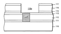
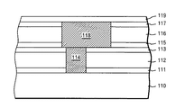
図6を参照すると、本発明の相互接続構造の好ましい実施形態は、トランジスタなどの論理回路要素を含むことができ、かつ以下に論じる伝導体およびキャップ層と同じかまたは異なる材料で形成されるシングル・ダマシン配線レベルまたはキャップ層あるいはその両方で終端させることのできる下部基板110を含む。例えば基板110は、タングステンを含む配線レベルで終端させることができ、一方、以下に論じる伝導体114および118は、銅で形成することができる。
Referring to FIG. 6, a preferred embodiment of the interconnect structure of the present invention can include a logic circuit element such as a transistor and is a single formed of the same or different material as the conductor and cap layers discussed below. Includes a
キャップ層111は、下部基板110上に堆積することができる。一般に層間誘電体(ILD)と呼ばれる誘電体層112は、キャップ層111上に重なっている。ビア・レベルのハードマスク層113は、ILD層112上に堆積することが好ましい。少なくとも1つのビア伝導体114は、ILD層112、キャップ層111、およびビア・ハードマスク層113に埋設されている。拡散障壁ライナ(図示せず)は、ILD層112とビア伝導体114との間に堆積することができる。ビア伝導体114の上面は、通常は化学機械研磨(CMP)ステップによって、ビア・ハードマスク層113の上面と同一平面になるよう作製されている。
The
第1の相互接続レベルは、図6に示す相互接続構造のキャップ層111、ILD層112、ハードマスク層113、およびビア伝導体114によって画定される。図2の第1の相互接続レベル上に示される第2の相互接続レベルは、ビア・キャップ層115、ILD層116、ライン・ハードマスク層117、およびライン伝導体118を含む。接着促進剤層(図示せず)は、ビア・キャップ層115とILD層116との間に堆積することができる。最終のキャップ層119は、ライン伝導体118およびライン・ハードマスク層117上に重なっている。
The first interconnect level is defined by the
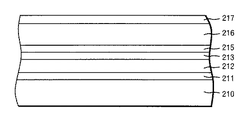
本発明の相互接続構造の別の好ましい実施形態を、図10に示す。この実施形態は、トランジスタなどの論理要素を含むことのできる下部基板210を含む。下部基板210上には、キャップ層211を堆積することができる。キャップ層211上にはILD層212が重なっている。ILD層212上にはエッチング・ストッパ層213が堆積される。エッチング・ストッパ層213上には接着促進剤層215が堆積される。接着促進剤層215上にはILD層216が堆積され、ILD層216上にはハードマスク層217が重なっている。少なくとも1つのビア伝導体214とライン伝導体218は、図示されるように、層211、212、213、215、216、および217に埋設されている。ライン伝導体218の上面は、ハードマスク層217の上面と同一平面になるように作製される。最終のキャップ層219は、ライン伝導体218およびハードマスク層217上に重なる。
Another preferred embodiment of the interconnect structure of the present invention is shown in FIG. This embodiment includes a
図6のILD層112、116、212、および216は、任意の適切な誘電体材料で作製することができるが、低k誘電体材料が好ましい。適切な誘電体材料には、炭素をドープした二酸化シリコン材料;フッ素化ケイ酸塩ガラス(FSG);有機ポリマー熱硬化性材料、シリコンオキシカーバイド;SiCOH誘電体;フッ素をドープした酸化シリコン;スピン・オン・ガラス(spin-on glass);水素シルセスキオキサン(HSQ)、メチルシルセスキオキサン(MSQ)、HSQとMSQの混合物またはコポリマーを含めたシルセスキオキサン;ベンゾシクロブテン(BCB)をベースにしたポリマー誘電体、および任意のシリコン含有低k誘電体が含まれる。シルセスキオキサンの化学的性質を使用したSiCOHタイプの組成を有するスピン・オン低k膜の例には、HOSP(商標)(ハネウェル(Honeywell)から入手可能)、JSR 5109および5108(日本合成ゴムから入手可能)、Zirkon(商標)(シップレイ・マイクロエレクトロニクス(ShipleyMicroelectronics)、ローム・アンド・ハース事業部(a division of Rohm and Haas)から入手可能)、および多孔質低k(ELK)材料(アプライド・マテリアル(AppliedMaterials)から入手可能)が含まれる。炭素をドープした二酸化シリコン材料またはオルガノシランの例には、Black Diamond(商標)(アプライド・マテリアル(AppliedMaterials)から入手可能)およびCoral(商標)(ノベラス(Novellus)から入手可能)が含まれる。HSQ材料の例は、FOx(商標)(ダウ・コーニング(DowCorning)から入手可能)である。好ましい誘電体材料には、本質的に炭素、酸素、および水素からなる有機ポリマー熱硬化性材料が含まれ、SiLK(商標)(ダウ・ケミカル・カンパニー(DowChemical Company)から入手可能)として知られる低kポリアリーレンエーテルポリマー材料およびFLARE(商標)(ハネウェル(Honeywell)から入手可能)として知られる低kポリマー材料が含まれる。 The ILD layers 112, 116, 212, and 216 of FIG. 6 can be made of any suitable dielectric material, but a low-k dielectric material is preferred. Suitable dielectric materials include carbon-doped silicon dioxide material; fluorinated silicate glass (FSG); organic polymer thermosetting material, silicon oxycarbide; SiCOH dielectric; fluorine-doped silicon oxide; Spin-on glass; silsesquioxane including hydrogen silsesquioxane (HSQ), methylsilsesquioxane (MSQ), a mixture or copolymer of HSQ and MSQ; benzocyclobutene (BCB) Included are polymer dielectrics based on and optional silicon-containing low-k dielectrics. Examples of spin-on low-k films having a SiCOH-type composition using silsesquioxane chemistry include HOSP ™ (available from Honeywell), JSR 5109 and 5108 (Japan Synthetic Rubber) Zirkon ™ (available from Shipley Microelectronics, a division of Rohm and Haas), and porous low-k (ELK) materials (Applied Materials (available from Applied Materials). Examples of carbon-doped silicon dioxide materials or organosilanes include Black Diamond ™ (available from Applied Materials) and Coral ™ (available from Novellus). An example of an HSQ material is FOx ™ (available from Dow Corning). Preferred dielectric materials include organic polymer thermosets consisting essentially of carbon, oxygen, and hydrogen, and are known as SiLK ™ (available from Dow Chemical Company). Included are k polyarylene ether polymer materials and low k polymer materials known as FLARE ™ (available from Honeywell).
好ましい実施形態では、信頼性を向上させるため、ビア・レベルのILD層112および212がSiCOHや酸化物誘電体材料などの熱膨張率(CTE:coefficient of thermal expansion)の低い材料で形成され、ライン・レベルのILD層116および216は、SiLK(商標)などの低kを有するポリマー熱硬化性材料で形成される。ビア・レベルのILD層112および212は、約50ppm/℃未満のCTEを有する誘電体材料で形成され、好ましくは伝導体114および214のCTEと一致するように形成されることが、特に好ましい。
In a preferred embodiment, via level ILD layers 112 and 212 are formed of a low coefficient of thermal expansion (CTE) material, such as SiCOH or oxide dielectric material, to improve reliability, The level ILD layers 116 and 216 are formed of a polymer thermoset material having a low k, such as SiLK ™. It is particularly preferred that the via level ILD layers 112 and 212 are formed of a dielectric material having a CTE of less than about 50 ppm / ° C., preferably to match the CTE of the
特に好ましい実施形態では、ビア・レベルのILD層112および212がSiCOHで形成され、ライン・レベルのILD層116および216がSiLK(商標)で形成される。別の実施形態では、ビア・レベルのILD層112および212をSiCOHで形成することができ、ライン・レベルのILD層116および216を多孔質SiLK(商標)で形成することができる。さらに別の実施形態では、ビア・レベルのILD層112および212を多孔質SiCOHで形成することができ、ライン・レベルのILD層116および216をSiLK(商標)で形成することができる。さらに別の実施形態では、ビア・レベルのILD層112および212を多孔質SiCOHで形成することができ、ライン・レベルのILD層116および216を多孔質SiLK(商標)で形成することができる。さらに別の実施形態では、ビア・レベルのILD層112および212を多孔質SiCOHで形成することができ、ライン・レベルのILD層116および216をSiCOHで形成することができる。さらに別の実施形態では、ビア・レベルのILD層112および212をSiCOHで形成することができ、ライン・レベルのILD層116および216を多孔質SiCOHで形成することができる。 In a particularly preferred embodiment, via level ILD layers 112 and 212 are formed of SiCOH, and line level ILD layers 116 and 216 are formed of SiLK ™. In another embodiment, the via level ILD layers 112 and 212 can be formed of SiCOH, and the line level ILD layers 116 and 216 can be formed of porous SiLK ™. In yet another embodiment, the via level ILD layers 112 and 212 can be formed of porous SiCOH, and the line level ILD layers 116 and 216 can be formed of SiLK ™. In yet another embodiment, the via level ILD layers 112 and 212 can be formed of porous SiCOH, and the line level ILD layers 116 and 216 can be formed of porous SiLK ™. In yet another embodiment, the via level ILD layers 112 and 212 can be formed of porous SiCOH, and the line level ILD layers 116 and 216 can be formed of SiCOH. In yet another embodiment, the via level ILD layers 112 and 212 can be formed of SiCOH, and the line level ILD layers 116 and 216 can be formed of porous SiCOH.
ILD層112、116、212、および216は、それぞれ厚さを約10nmから約1000nmにすることができるが、これらの層は、それぞれ約120nmの厚さであることが好ましい。ILD層112、116、212、および216に関する誘電率は、好ましくは約1.8から約3.5であり、最も好ましくは約2.5から約2.9である。ライン・レベルとビア・レベルの両方のILDに多孔質材料を使用した実施形態では、ILD層112、116、212、および216に関する材料が多孔質材料であり、それによって、これらの層の誘電率を約1.8から2.5の範囲までさらに低下させることができる。
The ILD layers 112, 116, 212, and 216 can each be about 10 nm to about 1000 nm thick, but these layers are preferably each about 120 nm thick. The dielectric constant for
ハードマスク層113およびエッチング・ストッパ層213は、任意の適切な誘電体材料で形成することができる。層113および213は、以下の特徴を有すること、すなわち(1)誘電率が低く(好ましくは約7未満);(2)ライナに比べてCMP速度が低く(好ましくは約1:5)、したがってCMPストッパ層として働き;(3)効果的なCMP後のクリーニングで水分を吸収し易く;(4)下に在る誘電体に拡散する銅の障壁として働き;(5)レジスト剥離操作中に使用される酸素プラズマに対して抵抗性があることが好ましい。層113および213に好ましい材料には、Blok(商標)(アプライド・マテリアル・インコーポレイテッド(Applied Materials, Inc.)から入手可能)などのSiCHおよびSiNCHが含まれ、約5未満の誘電率、好ましくは約4.9の誘電率を有する。具体的にこれらの層は、約20〜34原子%のシリコンと、約12〜34原子%の炭素と、約5〜30原子%の窒素と、約20〜50原子%の水素とからなることが好ましい。この材料は、好ましくは組成SixCyNwHzを有し、ただしxは約0.2から約0.34であり、yは約0.12から約0.34であり、wは約0.05から約0.3であり、zは約0.2から約0.5である。SiNCH材料に特に好ましい組成は、シリコンが約22〜30原子%、炭素が約15〜30原子%、窒素が約10〜22原子%、および水素が約30〜45原子%である。この特に好ましい組成は、SixCyNwHz、ただしxが約2.2から約3であり、yが約1.5から約3であり、wが約1から約2であり、zが約3から約4.5であるもので表される。最も好ましい実施形態は、複数のビア・ハードマスク層を利用し、その中で底部層が最も低い誘電率を有しかつ最高のCMP選択性を有する。
The
ビア・キャップ層115は、任意の適切な誘電体材料で形成することができる。ビア・キャップ層115は、以下の特徴を有すること、すなわち(1)誘電率が低く;(2)レジスト剥離操作中に使用される酸素プラズマに対して抵抗性があり;(3)銅障壁として働き;(4)エッチング選択性を有し、したがってエッチング・ストッパ層として働くことが好ましい。ビア・キャップ層115に特に好ましい材料は、誘電率が約5未満であり、かつシリコン、炭素、窒素、および水素を含んだ非晶質窒素化水素化シリコンカーバイド(SiCNH)である。その他の適切な材料には、SiN、SiCH、およびSiONが含まれる。
The via
接着促進剤層215は、以下の特徴を有すること、すなわち(1)誘電率が低く;(2)水分相互作用が低く;(3)耐酸化性が増大し;(4)ILD層216とビア・ハードマスク層213に対してRIEの化学的選択性を有することが好ましい。接着促進剤層215に特に好ましい材料には、シロキサンまたはSiCOHが含まれ、最も好ましくはHOSP BESt(商標)(ハネウェル(Honeywell)から入手可能)である。
The
ハードマスク層117および217は、任意の適切な誘電体材料で形成することができるが、誘電率が約5未満の誘電体材料で形成することが好ましい。ハードマスク層117および217に好ましい材料は、SiCOHおよびSiCHである。最も好ましい実施形態では、これらのハードマスク層は約3.5未満の誘電率を有する。 The hard mask layers 117 and 217 can be formed of any suitable dielectric material, but are preferably formed of a dielectric material having a dielectric constant less than about 5. Preferred materials for the hard mask layers 117 and 217 are SiCOH and SiCH. In the most preferred embodiment, these hard mask layers have a dielectric constant of less than about 3.5.
最終のキャップ層119および219は、任意の適切な誘電体材料で形成することができるが、SiNCHまたはSiNで形成することが好ましい。最終のキャップ層をSiNCHで形成する場合、この層は、約20〜34原子%のシリコンと、約12〜34原子%の炭素と、約5〜30原子%の窒素と、約20〜50原子%の水素とからなることが好ましい。この材料は、好ましくは組成SixCyNwHzを有し、ただしxは約0.2から約0.34であり、yは約0.12から約0.34であり、wは約0.05から約0.3であり、zは約0.2から約0.5である。SiNCH材料に特に好ましい組成は、シリコンが約22〜30原子%、炭素が約15〜30原子%、窒素が約10〜22原子%、水素が約30〜45原子%である。この特に好ましい組成は、SixCyNwHz、ただしxが約2.2から約3であり、yが約1.5から約3であり、wが約1から約2であり、zが約3から約4.5であるもので表すことができる。 The final cap layers 119 and 219 can be formed of any suitable dielectric material, but are preferably formed of SiNCH or SiN. When the final cap layer is formed of SiNCH, this layer is about 20-34 atomic percent silicon, about 12-34 atomic percent carbon, about 5-30 atomic percent nitrogen, and about 20-50 atomic percent. % Hydrogen. This material preferably has the composition Si x C y N w H z , where x is from about 0.2 to about 0.34, y is from about 0.12 to about 0.34, and w is About 0.05 to about 0.3 and z is about 0.2 to about 0.5. Particularly preferred compositions for SiNCH materials are about 22-30 atomic percent silicon, about 15-30 atomic percent carbon, about 10-22 atomic percent nitrogen, and about 30-45 atomic percent hydrogen. This particularly preferred composition is Si x C y N w H z , where x is from about 2.2 to about 3, y is from about 1.5 to about 3, and w is from about 1 to about 2. z can be expressed as being from about 3 to about 4.5.
図6の相互接続構造は、図2〜6に示すプロセスなどのシングル・ダマシン・プロセスによって形成することができる。このプロセスは、図2に示すように、任意選択で基板110上にキャップ層111を堆積することから始まり、その後、キャップ層111上にILD層112を堆積する。キャップ層111およびILD層112は、任意の適切な方法によって堆積することができる。例えばILD層112にSiLK(商標)を使用する場合は、樹脂をスピン・コーティング・プロセスによって塗布し、その後、ベーク・ステップにかけて溶媒を除去し、次いで熱硬化ステップにかけることができる。
The interconnect structure of FIG. 6 can be formed by a single damascene process, such as the process shown in FIGS. The process optionally begins with depositing a
次いで図2に示すように、ビア・レベルのハードマスク層113をILD層112上に堆積する。ハードマスク層113は任意の適切な方法によって堆積することができるが、ハードマスク層113がSiNCHである場合には、化学気相成長法(CVD)によってILD層112上に直接堆積することが好ましい。あるいは、ビア・レベルのハードマスク層113にはスピン・オン・ガラスを使用することができる。好ましいCVD材料の例はSiCHであり、好ましいスピン・オン材料の例はHOSP BESt(商標)である。
A via level
ハードマスク層113を堆積した後、追加の犠牲ハードマスク層(図示せず)を堆積することができる。例えば、2000年4月14日に出願された「相互接続構造を生成するための保護ハードマスク(Protective Hardmask for Producing Interconnect Structures)」という名称の同時係属の米国特許出願第09/550943号であって、その開示を参照により本明細書に援用するものに記載されるハードマスク層のような、一連のハードマスク層を堆積することができる。
After depositing the
キャップ層111、ILD層112、およびハードマスク層113を堆積した後、リソグラフィ・パターニング・プロセスを使用して、少なくとも1つのビア114aを形成する。ビア114aは、フォトレジストによって保護されていない領域で、例えば反応性イオン・エッチング(RIE)によってハードマスク層113およびILD層112の一部を除去することによって形成する。ハードマスク層113は、このエッチング・ステップを、以下のように補助することができる。ハードマスク層113は、まずそのフォトレジストで覆われていない領域をエッチングし、次いでそのフォトレジストを除去し、フォトレジスト・パターンに一致するパターニングされたハードマスク層113を残すことができる。ILD層112およびキャップ層111は、ハードマスク層113で覆われていない領域をエッチングすることができる。
After depositing the
ビア114aを形成した後、このビアに拡散障壁ライナを施し(図示せず)、次いで図3に示すように導体材料をビア114a内に堆積して伝導体114を形成する。拡散障壁ライナは、物理気相成長法(PVD)や化学気相成長法(CVD)、原子層堆積法(ALD)、イオン化物理気相成長法(I−PVD)などの任意の適切な方法によって堆積することができる。拡散障壁ライナは、薄膜複合体として数種の高融点金属(refractory metal)を堆積することによって構成された多層ライナでよい。導体材料114は、めっき技術などの任意の適切な方法によってビア114aに堆積することができる。過剰なライナ材料および過剰な導体材料114は、CMPプロセスで除去することができ、その場合、伝導体114の上面は、ハードマスク層113と同一平面に在るように作製される。ハードマスク層113は、このCMPステップ中に研磨ストッパ層として働き、それによってILD層112が研磨中に損傷を受けないようにする。犠牲ハードマスク層(図示せず)は、このCMPステップ中に除去してもよい。
After forming the via 114a, a diffusion barrier liner is applied to the via (not shown), and then a conductor material is deposited in the via 114a to form the
図2〜3は、キャップ層111、ILD層112、ハードマスク層113、およびビア伝導体115を含む第1の相互接続レベルの形成を示す。図4では、第2の相互接続レベルの形成が、ビア・キャップ層115、ILD層116、およびハードマスク層117の堆積から始まる。追加の犠牲ハードマスク層(図示せず)を主要なハードマスク層117上に堆積することができる。
2-3 illustrate the formation of a first interconnect level that includes a
好ましい実施形態では、キャップ層115は、CVDによって堆積した窒化シリコン膜である。特に好ましい実施形態では、キャップ層115は、CVDによって堆積したSiCNHである。
In a preferred embodiment, the
ILD層116は、ILD層112の材料とは異なる材料で形成することが好ましい。ILD層112がSiCOH材料で形成される場合(好ましくはCVDによって堆積した)、ILD層116は、SiLK(商標)などのポリマー熱硬化性材料で形成することが好ましい。ILD層116がSiLK(商標)などの低kポリマー材料である場合、典型的な場合にはそのILD材料をスピン塗布し、塗布後ホット・ベークにかけて溶媒を除去し、高温で硬化する。
The
ライン・ハードマスク層117は、SiCOHやSiCHなどの低k誘電体材料で形成することが好ましく、CVDまたはスピン塗布法によって堆積することができる。好ましいCVD材料の例はSiCHであり、好ましいスピン・オン材料の例はHOSP BESt(商標)である。
The line
ビア・キャップ層115、ILD層116、およびライン・ハードマスク層117の堆積後、リソグラフィ・パターニングおよび反応性イオン・エッチング(RIE)を含めてよいエッチング・プロセスを使用して、図4に示すように少なくとも1つのトレンチ118を形成する。トレンチ118には拡散障壁ライナ(図示せず)を施すことができ、次いで図5に示すように導体材料をトレンチ118a内に堆積して、伝導体118を形成する。拡散障壁ライナは、物理気相成長法(PVD)や化学気相成長法(CVD)、原子層堆積法(ALD)、イオン化物理気相成長法(I−PVD)などによる任意の適切な方法で堆積することができる。拡散障壁ライナは、薄膜複合体として数種の高融点金属を堆積することにより構成された多層ライナでよい。導体材料118は、典型的な場合、導体ビア114で使用したものと同じ材料であり、めっき技術などによる任意の適切な方法でトレンチ118a内に堆積することができる。過剰なライナ材料および過剰な導体材料118は、CMPプロセスで除去することができ、その場合、伝導体118の上面はライン・ハードマスク層117と同一平面になるよう作製される。
After deposition of via
伝導体114および118を形成した後は、図6に示すように最終のキャップ層119を堆積することができる。最終のキャップ層119は、任意の適切な誘電体材料で形成することができるが、好ましくはCVDによって堆積したSiCNHまたはSiNで形成される。
After forming the
上述のかつ図2〜6に示したシングル・ダマシン法の代替例として、本発明の相互接続構造は、図7〜10に示される方法などのデュアル・ダマシン法を使用して形成することができる。この代替プロセスは、任意選択で基板210上にキャップ層211を堆積することから始まり、その後、キャップ層211上にILD層212を堆積する。
As an alternative to the single damascene method described above and shown in FIGS. 2-6, the interconnect structure of the present invention can be formed using a dual damascene method, such as the method shown in FIGS. . This alternative process optionally begins with depositing a
次いでILD層212上に、まずエッチング・ストッパ層213を堆積し、次いでエッチング・ストッパ層213上に連続して接着促進剤層215を堆積することによって、2層エッチング・ストッパを構成する。層213は、CVDによって堆積することが好ましく、SiNCHが最も好ましい。接着促進剤層215は、好ましくはスピン塗布法によって堆積され、好ましくはSiCOH材料であり、最も好ましくはHOSP BESt(商標)である。
Next, an
接着剤促進剤層215を堆積した後に、ILD層216およびハードマスク層217を堆積する。次いで従来のリソグラフィ・プロセスを使用して、図8に示すように、トレンチ218aおよびビア214aを形成する。デュアル・ダマシン・エッチング・プロセスでは、犠牲ハードマスクを利用する。ライン・レベルのリソグラフィを実施した後、エッチング・プロセスによって、ライン・レベルのパターンは非犠牲層217以外のハードマスク・レベルに転写される。次いでリソグラフィを実施して、ビア・レベルをパターニングする。エッチング・プロセスでは、全ハードマスク・スタック(層217を含む)およびILD層216を除去し、層215上で選択的に停止することによって、ビア214aのパターンを転写する。次に、残されているライン・レベルのハードマスク層(層217を含む)をエッチングする。エッチング・プロセスは、ビア・パターンを層215、213、および212にエッチングすることによって継続し、層211上で選択的に停止させる。ILD層212は、ラインがさらに画定されるようエッチングする。最後に、キャップ層211をエッチングしてビアを完成させる。この最終のエッチング・ステップでは、ライン・パターン内の層215を除去してトレンチ218aも完成させる。
After depositing the
次いでビア214aおよびトレンチ218aには、デュアル・ダマシン・プロセスで導体材料を充填して、図9に示すように伝導体214、218を形成する。過剰な導体材料は、上述のようにCMPプロセスで除去することができる。
The
伝導体214、218を形成した後、最終のキャップ層219を図10に示すように堆積することができる。最終のキャップ層219は、任意の適切な誘電体材料で形成することができるが、CVDによってSiCNHまたはSiNで形成することが好ましい。
After forming the
図7〜10に示すデュアル・ダマシン法の代替例として、本発明の相互接続構造は、以下の単純化したデュアル・ダマシン法を使用して形成することができる。この代替のデュアル・ダマシン法では、ILD層212の性質を、RIEパターニング・ステップでの選択性に合わせて調節することができ、このRIEステップでの化学的作用は、例えば層216と層212とを異なる材料にし、それによって埋設された層213および215を構造から省略することによって、調節することができる。例えば、CF4を使用してSiCOH材料をエッチングすることができ、N2/H2を使用して、SiLKなどのポリマー材料をエッチングすることができる。
As an alternative to the dual damascene method shown in FIGS. 7-10, the interconnect structure of the present invention can be formed using the following simplified dual damascene method. In this alternative dual damascene method, the nature of the
本発明について、特定の好ましい実施形態およびその他の代替の実施形態と併せて詳細に延べてきたが、前述の内容に照らして非常に数多くの代替例、修正例、および変形例が当業者に明らかになることが明白である。したがって上述の特許請求の範囲は、そのような代替例、修正例、および変形例のすべてが本発明の真の範囲および精神に含まれるとして解釈されるものである。 While the invention has been described in detail in conjunction with certain preferred embodiments and other alternative embodiments, numerous alternatives, modifications and variations will be apparent to those skilled in the art in light of the foregoing. It is clear that Accordingly, the appended claims are to be construed as including all such alternatives, modifications, and variations that fall within the true scope and spirit of the present invention.
Claims (32)
前記第1の誘電体層上に在りかつ上面を有する第1のハードマスク層と、
前記第1の誘電体層および前記第1のハードマスク層に埋設された少なくとも1つの導体ビアと、
前記第1のハードマスク層上のビア・レベル・キャップ層と、
前記ビア・レベル・キャップ層上に在る第2の誘電体層であって、前記第1の誘電体層とは異なる材料で形成された第2の誘電体層と、
前記第2の誘電体層上に在りかつ上面を有する第2のハードマスク層と、
前記ビア・レベル・キャップ層、前記第2の誘電体層、および前記第2のハードマスク層に埋設され、かつ前記第2のハードマスク層の上面と同一平面に在る上面を有している、少なくとも1つの導体ラインと
を含む、基板上に形成された相互接続構造。 A first dielectric layer overlying the substrate;
A first hard mask layer overlying the first dielectric layer and having an upper surface;
At least one conductor via embedded in the first dielectric layer and the first hard mask layer;
A via level cap layer on the first hardmask layer;
A second dielectric layer overlying the via level cap layer, the second dielectric layer formed of a material different from the first dielectric layer;
A second hard mask layer overlying the second dielectric layer and having an upper surface;
The upper surface is embedded in the via level cap layer, the second dielectric layer, and the second hard mask layer and is flush with the upper surface of the second hard mask layer. An interconnect structure formed on a substrate, comprising: at least one conductor line.
前記第1の誘電体層上のエッチング・ストッパ層と、
前記エッチング・ストッパ層上の接着促進剤層と、
前記接着促進剤層上の第2の誘電体層であって、前記第1の誘電体層とは異なる材料で形成された第2の誘電体層と、
前記第2の誘電体層上に在りかつ上面を有するハードマスク層と、
前記第1の誘電体層および前記エッチング・ストッパ層に埋設された少なくとも1つの導体ビアと、
前記接着促進剤層、前記第2の誘電体層、および前記ハードマスク層に埋設され、かつ前記ハードマスク層の上面と同一平面に在る上面を有する少なくとも1つの導体ラインと
を含む、基板上に形成された相互接続構造。 A first dielectric layer overlying the substrate;
An etching stopper layer on the first dielectric layer;
An adhesion promoter layer on the etching stopper layer;
A second dielectric layer on the adhesion promoter layer, the second dielectric layer formed of a different material from the first dielectric layer;
A hard mask layer overlying the second dielectric layer and having an upper surface;
At least one conductor via embedded in the first dielectric layer and the etching stopper layer;
On the substrate, comprising: the adhesion promoter layer; the second dielectric layer; and at least one conductor line embedded in the hard mask layer and having an upper surface that is coplanar with the upper surface of the hard mask layer Interconnect structure formed into.
前記第1の誘電体層上に、上面を有する第1のハードマスク層を堆積するステップと、
前記第1の誘電体層および前記第1のハードマスク層に少なくとも1つのビア開口を形成するステップと、
前記ビア開口に導体材料を充填するステップであって、それによって前記第1の誘電体層および前記第1のハードマスク層に埋設された少なくとも1個の導体ビアを形成するステップと、
前記第1のハードマスク層上にビア・レベルのキャップ層を堆積するステップと、
前記ビア・レベルのキャップ層上に第2の誘電体層を堆積するステップであって、前記第2の誘電体層が前記第1の誘電体層とは異なる材料で形成されたものであるステップと、
前記第2の誘電体層上に、上面を有する第2のハードマスク層を堆積するステップと、
前記ビア・レベルのキャップ層、前記第2の誘電体層、および前記ハードマスク層に少なくとも1つのトレンチ開口を形成するステップであって、前記トレンチ開口が前記第1の導体ビア上に重なるものであるステップと、
前記トレンチ開口に導体材料を充填するステップであって、それによって、前記ビア・レベルのキャップ層、前記第2の誘電体層、および前記第2のハードマスク層に埋設された少なくとも1つの導体ラインを形成し、前記導体ラインが、前記第2のハードマスク層の上面と同一平面に在る上面を有するものであるステップと
を含む、基板上に相互接続構造を形成する方法。 Depositing a first dielectric layer on a substrate;
Depositing a first hard mask layer having an upper surface on the first dielectric layer;
Forming at least one via opening in the first dielectric layer and the first hard mask layer;
Filling the via opening with a conductive material, thereby forming at least one conductive via embedded in the first dielectric layer and the first hard mask layer;
Depositing a via level cap layer on the first hardmask layer;
Depositing a second dielectric layer on the via level cap layer, wherein the second dielectric layer is formed of a different material than the first dielectric layer; When,
Depositing a second hard mask layer having an upper surface on the second dielectric layer;
Forming at least one trench opening in the via level cap layer, the second dielectric layer, and the hard mask layer, the trench opening overlying the first conductor via; A step and
At least one conductor line embedded in the via-level cap layer, the second dielectric layer, and the second hard mask layer by filling the trench opening with a conductor material; And forming the interconnect structure on the substrate, wherein the conductor line has an upper surface that is coplanar with the upper surface of the second hard mask layer.
前記第1の誘電体層上に、上面を有するエッチング・ストッパ層を堆積するステップと、
前記エッチング・ストッパ層上に接着促進剤層を堆積するステップと、
前記接着促進剤層上に第2の誘電体層を堆積するステップであって、前記第2の誘電体層が前記第1の誘電体層とは異なる材料で形成されるものであるステップと、
前記第2の誘電体層上に、上面を有するハードマスク層を堆積するステップと、
前記ハードマスク層、前記第2の誘電体層、前記接着促進剤層、前記第1の誘電体層、および前記エッチング・ストッパ層に、少なくとも1つのビア開口を形成するステップと、
前記ハードマスク層、前記第2の誘電体層、および前記接着促進剤層に少なくとも1つのトレンチ開口を形成するステップであって、前記トレンチ開口が前記ビア開口上に重なるものであるステップと、
前記ビアおよびトレンチ開口に導体材料を充填するステップであって、それによって、前記第1の誘電体層、前記エッチング・ストッパ層、前記接着促進剤層、前記第2の誘電体層、および前記ハードマスク層に埋設された少なくとも1つのビア伝導体および少なくとも1個のライン伝導体を形成し、前記ライン伝導体が、前記ハードマスク層の上面と同一平面に在る上面を有するものであるステップとを含む、基板上に相互接続構造を形成する方法。 Depositing a first dielectric layer on a substrate;
Depositing an etching stopper layer having an upper surface on the first dielectric layer;
Depositing an adhesion promoter layer on the etching stopper layer;
Depositing a second dielectric layer on the adhesion promoter layer, wherein the second dielectric layer is formed of a material different from the first dielectric layer;
Depositing a hard mask layer having an upper surface on the second dielectric layer;
Forming at least one via opening in the hard mask layer, the second dielectric layer, the adhesion promoter layer, the first dielectric layer, and the etching stopper layer;
Forming at least one trench opening in the hard mask layer, the second dielectric layer, and the adhesion promoter layer, wherein the trench opening overlaps the via opening;
Filling the via and trench openings with a conductive material, whereby the first dielectric layer, the etching stopper layer, the adhesion promoter layer, the second dielectric layer, and the hard Forming at least one via conductor and at least one line conductor embedded in the mask layer, wherein the line conductor has a top surface that is coplanar with the top surface of the hard mask layer; Forming an interconnect structure on a substrate.
Applications Claiming Priority (2)
| Application Number | Priority Date | Filing Date | Title |
|---|---|---|---|
| US10/294,139 US6917108B2 (en) | 2002-11-14 | 2002-11-14 | Reliable low-k interconnect structure with hybrid dielectric |
| PCT/GB2003/004814 WO2004044978A1 (en) | 2002-11-14 | 2003-11-07 | Reliable low-k interconnect structure with hybrid dielectric |
Related Child Applications (1)
| Application Number | Title | Priority Date | Filing Date |
|---|---|---|---|
| JP2010247790A Division JP2011061228A (en) | 2002-11-14 | 2010-11-04 | High reliability low dielectric constant interconnect structure provided with hybrid dielectric body |
Publications (2)
| Publication Number | Publication Date |
|---|---|
| JP2006506806A true JP2006506806A (en) | 2006-02-23 |
| JP2006506806A5 JP2006506806A5 (en) | 2006-12-07 |
Family
ID=32296906
Family Applications (2)
| Application Number | Title | Priority Date | Filing Date |
|---|---|---|---|
| JP2004550790A Pending JP2006506806A (en) | 2002-11-14 | 2003-11-07 | Reliable low dielectric constant interconnect structure with hybrid dielectric |
| JP2010247790A Pending JP2011061228A (en) | 2002-11-14 | 2010-11-04 | High reliability low dielectric constant interconnect structure provided with hybrid dielectric body |
Family Applications After (1)
| Application Number | Title | Priority Date | Filing Date |
|---|---|---|---|
| JP2010247790A Pending JP2011061228A (en) | 2002-11-14 | 2010-11-04 | High reliability low dielectric constant interconnect structure provided with hybrid dielectric body |
Country Status (8)
| Country | Link |
|---|---|
| US (2) | US6917108B2 (en) |
| EP (1) | EP1561241A1 (en) |
| JP (2) | JP2006506806A (en) |
| KR (1) | KR100773003B1 (en) |
| CN (1) | CN1314101C (en) |
| AU (1) | AU2003279460A1 (en) |
| TW (1) | TWI234231B (en) |
| WO (1) | WO2004044978A1 (en) |
Cited By (3)
| Publication number | Priority date | Publication date | Assignee | Title |
|---|---|---|---|---|
| JP2010267971A (en) * | 2009-05-13 | 2010-11-25 | Air Products & Chemicals Inc | Dielectric barrier deposition using nitrogen containing precursor |
| JP2012190900A (en) * | 2011-03-09 | 2012-10-04 | Sony Corp | Semiconductor device and method of manufacturing the same |
| US11384429B2 (en) | 2008-04-29 | 2022-07-12 | Applied Materials, Inc. | Selective cobalt deposition on copper surfaces |
Families Citing this family (45)
| Publication number | Priority date | Publication date | Assignee | Title |
|---|---|---|---|---|
| US7425346B2 (en) * | 2001-02-26 | 2008-09-16 | Dielectric Systems, Inc. | Method for making hybrid dielectric film |
| JP2004146798A (en) * | 2002-09-30 | 2004-05-20 | Sanyo Electric Co Ltd | Semiconductor device and manufacturing method therefor |
| JP3898133B2 (en) * | 2003-01-14 | 2007-03-28 | Necエレクトロニクス株式会社 | A method of forming a SiCHN film. |
| JP3715626B2 (en) * | 2003-01-17 | 2005-11-09 | 株式会社東芝 | Semiconductor device manufacturing method and semiconductor device |
| JP4086673B2 (en) * | 2003-02-04 | 2008-05-14 | Necエレクトロニクス株式会社 | Semiconductor device and manufacturing method thereof |
| US7081673B2 (en) * | 2003-04-17 | 2006-07-25 | International Business Machines Corporation | Multilayered cap barrier in microelectronic interconnect structures |
| US6919636B1 (en) * | 2003-07-31 | 2005-07-19 | Advanced Micro Devices, Inc. | Interconnects with a dielectric sealant layer |
| US7199046B2 (en) * | 2003-11-14 | 2007-04-03 | Tokyo Electron Ltd. | Structure comprising tunable anti-reflective coating and method of forming thereof |
| US20050130407A1 (en) * | 2003-12-12 | 2005-06-16 | Jui-Neng Tu | Dual damascene process for forming a multi-layer low-k dielectric interconnect |
| US7224068B2 (en) * | 2004-04-06 | 2007-05-29 | Taiwan Semiconductor Manufacturing Company, Ltd. | Stable metal structure with tungsten plug |
| US20060012014A1 (en) * | 2004-07-15 | 2006-01-19 | International Business Machines Corporation | Reliability of low-k dielectric devices with energy dissipative layer |
| US20060027924A1 (en) * | 2004-08-03 | 2006-02-09 | Taiwan Semiconductor Manufacturing Co., Ltd. | Metallization layers for crack prevention and reduced capacitance |
| US6974772B1 (en) * | 2004-08-19 | 2005-12-13 | Intel Corporation | Integrated low-k hard mask |
| US7348672B2 (en) * | 2005-07-07 | 2008-03-25 | Taiwan Semiconductor Manufacturing Co., Ltd. | Interconnects with improved reliability |
| US7341941B2 (en) * | 2005-08-19 | 2008-03-11 | Texas Instruments Incorporated | Methods to facilitate etch uniformity and selectivity |
| US7394154B2 (en) * | 2005-09-13 | 2008-07-01 | International Business Machines Corporation | Embedded barrier for dielectric encapsulation |
| US20070059922A1 (en) * | 2005-09-13 | 2007-03-15 | International Business Machines Corporation | Post-etch removal of fluorocarbon-based residues from a hybrid dielectric structure |
| US7749730B2 (en) * | 2005-11-03 | 2010-07-06 | Redpoint Bio Corporation | High throughput screening assay for the TRPM5 ion channel |
| US20070155186A1 (en) * | 2005-11-22 | 2007-07-05 | International Business Machines Corporation | OPTIMIZED SiCN CAPPING LAYER |
| US7338893B2 (en) * | 2005-11-23 | 2008-03-04 | Texas Instruments Incorporated | Integration of pore sealing liner into dual-damascene methods and devices |
| US7358182B2 (en) * | 2005-12-22 | 2008-04-15 | International Business Machines Corporation | Method of forming an interconnect structure |
| US20070152332A1 (en) * | 2006-01-04 | 2007-07-05 | International Business Machines Corporation | Single or dual damascene via level wirings and/or devices, and methods of fabricating same |
| US7473636B2 (en) * | 2006-01-12 | 2009-01-06 | International Business Machines Corporation | Method to improve time dependent dielectric breakdown |
| US20070278682A1 (en) * | 2006-05-31 | 2007-12-06 | Chung-Chi Ko | Self-assembled mono-layer liner for cu/porous low-k interconnections |
| US7727885B2 (en) * | 2006-08-29 | 2010-06-01 | Texas Instruments Incorporated | Reduction of punch-thru defects in damascene processing |
| US7466027B2 (en) * | 2006-09-13 | 2008-12-16 | Taiwan Semiconductor Manufacturing Co., Ltd. | Interconnect structures with surfaces roughness improving liner and methods for fabricating the same |
| US7749894B2 (en) * | 2006-11-09 | 2010-07-06 | Chartered Semiconductor Manufacturing Ltd. | Integrated circuit processing system |
| US7723226B2 (en) * | 2007-01-17 | 2010-05-25 | Taiwan Semiconductor Manufacturing Company, Ltd. | Interconnects containing bilayer porous low-k dielectrics using different porogen to structure former ratio |
| US7947565B2 (en) | 2007-02-07 | 2011-05-24 | United Microelectronics Corp. | Forming method of porous low-k layer and interconnect process |
| US7485949B2 (en) * | 2007-05-02 | 2009-02-03 | Taiwan Semiconductor Manufacturing Co., Ltd. | Semiconductor device |
| US7718525B2 (en) | 2007-06-29 | 2010-05-18 | International Business Machines Corporation | Metal interconnect forming methods and IC chip including metal interconnect |
| US20090032491A1 (en) * | 2007-08-03 | 2009-02-05 | International Business Machines Corporation | Conductive element forming using sacrificial layer patterned to form dielectric layer |
| US20090176367A1 (en) * | 2008-01-08 | 2009-07-09 | Heidi Baks | OPTIMIZED SiCN CAPPING LAYER |
| US8212337B2 (en) | 2008-01-10 | 2012-07-03 | International Business Machines Corporation | Advanced low k cap film formation process for nano electronic devices |
| US7863176B2 (en) * | 2008-05-13 | 2011-01-04 | Micron Technology, Inc. | Low-resistance interconnects and methods of making same |
| JP2010003894A (en) * | 2008-06-20 | 2010-01-07 | Nec Electronics Corp | Method for manufacturing semiconductor device, and the semiconductor device |
| US8189292B2 (en) * | 2008-12-24 | 2012-05-29 | Hitachi Global Storage Technologies Netherlands B.V. | Method for manufacturing a magnetic write head having a write pole with a trailing edge taper using a Rieable hard mask |
| US8836127B2 (en) * | 2009-11-19 | 2014-09-16 | Taiwan Semiconductor Manufacturing Co., Ltd. | Interconnect with flexible dielectric layer |
| US8461683B2 (en) * | 2011-04-01 | 2013-06-11 | Intel Corporation | Self-forming, self-aligned barriers for back-end interconnects and methods of making same |
| US8980740B2 (en) | 2013-03-06 | 2015-03-17 | Globalfoundries Inc. | Barrier layer conformality in copper interconnects |
| US9385086B2 (en) * | 2013-12-10 | 2016-07-05 | Taiwan Semiconductor Manufacturing Co., Ltd. | Bi-layer hard mask for robust metallization profile |
| US9905456B1 (en) * | 2016-09-26 | 2018-02-27 | Taiwan Semiconductor Manufacturing Co., Ltd. | Semiconductor device and manufacturing method thereof |
| US10256191B2 (en) | 2017-01-23 | 2019-04-09 | International Business Machines Corporation | Hybrid dielectric scheme for varying liner thickness and manganese concentration |
| US11217481B2 (en) * | 2019-11-08 | 2022-01-04 | International Business Machines Corporation | Fully aligned top vias |
| US11244854B2 (en) | 2020-03-24 | 2022-02-08 | International Business Machines Corporation | Dual damascene fully aligned via in interconnects |
Citations (3)
| Publication number | Priority date | Publication date | Assignee | Title |
|---|---|---|---|---|
| WO2000079586A1 (en) * | 1999-06-24 | 2000-12-28 | Hitachi, Ltd. | Production method for semiconductor integrated circuit device and semiconductor integrated circuit device |
| JP2001284454A (en) * | 2000-02-29 | 2001-10-12 | Internatl Business Mach Corp <Ibm> | Multi-level coface interconnecting structure |
| US20020164889A1 (en) * | 2001-05-02 | 2002-11-07 | Cheng-Yuan Tsai | Method for improving adhesion of low k materials with adjacent layer |
Family Cites Families (43)
| Publication number | Priority date | Publication date | Assignee | Title |
|---|---|---|---|---|
| US6265780B1 (en) | 1998-12-01 | 2001-07-24 | United Microelectronics Corp. | Dual damascene structure for the wiring-line structures of multi-level interconnects in integrated circuit |
| US6245662B1 (en) | 1998-07-23 | 2001-06-12 | Applied Materials, Inc. | Method of producing an interconnect structure for an integrated circuit |
| US6265779B1 (en) * | 1998-08-11 | 2001-07-24 | International Business Machines Corporation | Method and material for integration of fuorine-containing low-k dielectrics |
| JP2000150516A (en) | 1998-09-02 | 2000-05-30 | Tokyo Electron Ltd | Fabrication of semiconductor device |
| US6159842A (en) | 1999-01-11 | 2000-12-12 | Taiwan Semiconductor Manufacturing Company | Method for fabricating a hybrid low-dielectric-constant intermetal dielectric (IMD) layer with improved reliability for multilevel interconnections |
| US6187663B1 (en) | 1999-01-19 | 2001-02-13 | Taiwan Semiconductor Manufacturing Company | Method of optimizing device performance via use of copper damascene structures, and HSQ/FSG, hybrid low dielectric constant materials |
| US6380091B1 (en) | 1999-01-27 | 2002-04-30 | Advanced Micro Devices, Inc. | Dual damascene arrangement for metal interconnection with oxide dielectric layer and low K dielectric constant layer |
| US6312793B1 (en) * | 1999-05-26 | 2001-11-06 | International Business Machines Corporation | Multiphase low dielectric constant material |
| US6770975B2 (en) | 1999-06-09 | 2004-08-03 | Alliedsignal Inc. | Integrated circuits with multiple low dielectric-constant inter-metal dielectrics |
| US6319814B1 (en) * | 1999-10-12 | 2001-11-20 | United Microelectronics Corp. | Method of fabricating dual damascene |
| US6406994B1 (en) | 1999-12-03 | 2002-06-18 | Chartered Semiconductor Manufacturing Ltd. | Triple-layered low dielectric constant dielectric dual damascene approach |
| FR2802336B1 (en) * | 1999-12-13 | 2002-03-01 | St Microelectronics Sa | DAMASCENE-TYPE INTERCONNECTION STRUCTURE AND ITS MANUFACTURING METHOD |
| US6362091B1 (en) | 2000-03-14 | 2002-03-26 | Intel Corporation | Method for making a semiconductor device having a low-k dielectric layer |
| US6440878B1 (en) * | 2000-04-03 | 2002-08-27 | Sharp Laboratories Of America, Inc. | Method to enhance the adhesion of silicon nitride to low-k fluorinated amorphous carbon using a silicon carbide adhesion promoter layer |
| JP2001338978A (en) | 2000-05-25 | 2001-12-07 | Hitachi Ltd | Semiconductor device and its manufacturing method |
| US6358842B1 (en) | 2000-08-07 | 2002-03-19 | Chartered Semiconductor Manufacturing Ltd. | Method to form damascene interconnects with sidewall passivation to protect organic dielectrics |
| KR100795714B1 (en) | 2000-08-21 | 2008-01-21 | 다우 글로벌 테크놀로지스 인크. | Organosilicate resins as hardmasks for organic polymer dielectrics in fabrication of microelectronic devices |
| US6451683B1 (en) | 2000-08-28 | 2002-09-17 | Micron Technology, Inc. | Damascene structure and method of making |
| US6395632B1 (en) | 2000-08-31 | 2002-05-28 | Micron Technology, Inc. | Etch stop in damascene interconnect structure and method of making |
| US6472306B1 (en) | 2000-09-05 | 2002-10-29 | Industrial Technology Research Institute | Method of forming a dual damascene opening using CVD Low-K material and spin-on-polymer |
| US6380084B1 (en) * | 2000-10-02 | 2002-04-30 | Chartered Semiconductor Manufacturing Inc. | Method to form high performance copper damascene interconnects by de-coupling via and metal line filling |
| SG137694A1 (en) * | 2000-10-25 | 2007-12-28 | Ibm | Ultralow dielectric constant material as an intralevel or interlevel dieletric in a semiconductor device and electronic device containing the same |
| TW468241B (en) * | 2000-11-14 | 2001-12-11 | United Microelectronics Corp | Method to improve adhesion of dielectric material of semiconductor |
| JP2002164428A (en) * | 2000-11-29 | 2002-06-07 | Hitachi Ltd | Semiconductor device and its manufacturing method |
| US6451712B1 (en) * | 2000-12-18 | 2002-09-17 | International Business Machines Corporation | Method for forming a porous dielectric material layer in a semiconductor device and device formed |
| TWI272694B (en) * | 2001-01-03 | 2007-02-01 | Dow Corning | Metal ion diffusion barrier layers |
| US6383920B1 (en) | 2001-01-10 | 2002-05-07 | International Business Machines Corporation | Process of enclosing via for improved reliability in dual damascene interconnects |
| US6603204B2 (en) | 2001-02-28 | 2003-08-05 | International Business Machines Corporation | Low-k interconnect structure comprised of a multilayer of spin-on porous dielectrics |
| US6677680B2 (en) | 2001-02-28 | 2004-01-13 | International Business Machines Corporation | Hybrid low-k interconnect structure comprised of 2 spin-on dielectric materials |
| US6710450B2 (en) * | 2001-02-28 | 2004-03-23 | International Business Machines Corporation | Interconnect structure with precise conductor resistance and method to form same |
| KR20040005920A (en) | 2001-04-16 | 2004-01-16 | 허니웰 인터내셔날 인코포레이티드 | Layered stacks and methods of production thereof |
| KR100416596B1 (en) * | 2001-05-10 | 2004-02-05 | 삼성전자주식회사 | Method of manufacturing interconnection wire in semiconductor device |
| US6391757B1 (en) | 2001-06-06 | 2002-05-21 | United Microelectronics Corp. | Dual damascene process |
| US6879046B2 (en) * | 2001-06-28 | 2005-04-12 | Agere Systems Inc. | Split barrier layer including nitrogen-containing portion and oxygen-containing portion |
| US6798043B2 (en) | 2001-06-28 | 2004-09-28 | Agere Systems, Inc. | Structure and method for isolating porous low-k dielectric films |
| JP4152619B2 (en) * | 2001-11-14 | 2008-09-17 | 株式会社ルネサステクノロジ | Semiconductor device and manufacturing method thereof |
| US20030134499A1 (en) * | 2002-01-15 | 2003-07-17 | International Business Machines Corporation | Bilayer HDP CVD / PE CVD cap in advanced BEOL interconnect structures and method thereof |
| US6806203B2 (en) * | 2002-03-18 | 2004-10-19 | Applied Materials Inc. | Method of forming a dual damascene structure using an amorphous silicon hard mask |
| JP4340040B2 (en) * | 2002-03-28 | 2009-10-07 | 富士通マイクロエレクトロニクス株式会社 | Manufacturing method of semiconductor device |
| JP3657921B2 (en) * | 2002-04-26 | 2005-06-08 | 株式会社東芝 | Semiconductor device and manufacturing method thereof |
| US6764774B2 (en) * | 2002-06-19 | 2004-07-20 | International Business Machines Corporation | Structures with improved adhesion to Si and C containing dielectrics and method for preparing the same |
| US6867125B2 (en) * | 2002-09-26 | 2005-03-15 | Intel Corporation | Creating air gap in multi-level metal interconnects using electron beam to remove sacrificial material |
| US7023093B2 (en) * | 2002-10-24 | 2006-04-04 | International Business Machines Corporation | Very low effective dielectric constant interconnect Structures and methods for fabricating the same |
-
2002
- 2002-11-14 US US10/294,139 patent/US6917108B2/en not_active Expired - Lifetime
-
2003
- 2003-10-30 TW TW092130322A patent/TWI234231B/en not_active IP Right Cessation
- 2003-11-07 KR KR1020057008490A patent/KR100773003B1/en not_active IP Right Cessation
- 2003-11-07 AU AU2003279460A patent/AU2003279460A1/en not_active Abandoned
- 2003-11-07 CN CNB2003801033040A patent/CN1314101C/en not_active Expired - Lifetime
- 2003-11-07 WO PCT/GB2003/004814 patent/WO2004044978A1/en active Application Filing
- 2003-11-07 JP JP2004550790A patent/JP2006506806A/en active Pending
- 2003-11-07 EP EP03772408A patent/EP1561241A1/en not_active Withdrawn
-
2004
- 2004-07-29 US US10/901,868 patent/US7135398B2/en not_active Expired - Lifetime
-
2010
- 2010-11-04 JP JP2010247790A patent/JP2011061228A/en active Pending
Patent Citations (3)
| Publication number | Priority date | Publication date | Assignee | Title |
|---|---|---|---|---|
| WO2000079586A1 (en) * | 1999-06-24 | 2000-12-28 | Hitachi, Ltd. | Production method for semiconductor integrated circuit device and semiconductor integrated circuit device |
| JP2001284454A (en) * | 2000-02-29 | 2001-10-12 | Internatl Business Mach Corp <Ibm> | Multi-level coface interconnecting structure |
| US20020164889A1 (en) * | 2001-05-02 | 2002-11-07 | Cheng-Yuan Tsai | Method for improving adhesion of low k materials with adjacent layer |
Cited By (4)
| Publication number | Priority date | Publication date | Assignee | Title |
|---|---|---|---|---|
| US11384429B2 (en) | 2008-04-29 | 2022-07-12 | Applied Materials, Inc. | Selective cobalt deposition on copper surfaces |
| US11959167B2 (en) | 2008-04-29 | 2024-04-16 | Applied Materials, Inc. | Selective cobalt deposition on copper surfaces |
| JP2010267971A (en) * | 2009-05-13 | 2010-11-25 | Air Products & Chemicals Inc | Dielectric barrier deposition using nitrogen containing precursor |
| JP2012190900A (en) * | 2011-03-09 | 2012-10-04 | Sony Corp | Semiconductor device and method of manufacturing the same |
Also Published As
| Publication number | Publication date |
|---|---|
| TWI234231B (en) | 2005-06-11 |
| AU2003279460A1 (en) | 2004-06-03 |
| WO2004044978A1 (en) | 2004-05-27 |
| JP2011061228A (en) | 2011-03-24 |
| KR100773003B1 (en) | 2007-11-05 |
| CN1314101C (en) | 2007-05-02 |
| CN1711635A (en) | 2005-12-21 |
| US20050023693A1 (en) | 2005-02-03 |
| US6917108B2 (en) | 2005-07-12 |
| EP1561241A1 (en) | 2005-08-10 |
| US20040094839A1 (en) | 2004-05-20 |
| US7135398B2 (en) | 2006-11-14 |
| KR20050074996A (en) | 2005-07-19 |
| TW200419714A (en) | 2004-10-01 |
Similar Documents
| Publication | Publication Date | Title |
|---|---|---|
| JP2006506806A (en) | Reliable low dielectric constant interconnect structure with hybrid dielectric | |
| US6939797B2 (en) | Advanced BEOL interconnect structures with low-k PE CVD cap layer and method thereof | |
| US6914320B2 (en) | Bilayer HDP CVD/PE CVD cap in advanced BEOL interconnect structures and method thereof | |
| US7541276B2 (en) | Methods for forming dual damascene wiring for semiconductor devices using protective via capping layer | |
| US7259090B2 (en) | Copper damascene integration scheme for improved barrier layers | |
| US6617232B2 (en) | Method of forming wiring using a dual damascene process | |
| JP2004146800A (en) | Manufacturing method and structure of interconnection structure | |
| US20080251929A1 (en) | Semiconductor Device and Semiconductor Device Manufacturing Method | |
| US9870944B2 (en) | Back-end-of-line (BEOL) interconnect structure | |
| US6927113B1 (en) | Semiconductor component and method of manufacture | |
| JP5400355B2 (en) | Semiconductor device | |
| US20070222076A1 (en) | Single or dual damascene structure reducing or eliminating the formation of micro-trenches arising from lithographic misalignment | |
| US6774031B2 (en) | Method of forming dual-damascene structure | |
| JP4558272B2 (en) | Chrome adhesion layer for copper vias in low dielectric constant technology | |
| US20060118955A1 (en) | Robust copper interconnection structure and fabrication method thereof | |
| JP5047504B2 (en) | Method for manufacturing dual damascene wiring of semiconductor device using via capping protective film | |
| KR100562630B1 (en) | Copper vias in low-k technology | |
| US7250364B2 (en) | Semiconductor devices with composite etch stop layers and methods of fabrication thereof | |
| US6403471B1 (en) | Method of forming a dual damascene structure including smoothing the top part of a via | |
| JP4206740B2 (en) | Semiconductor device |
Legal Events
| Date | Code | Title | Description |
|---|---|---|---|
| A529 | Written submission of copy of amendment under section 34 (pct) |
Free format text: JAPANESE INTERMEDIATE CODE: A529 Effective date: 20050713 |
|
| A521 | Written amendment |
Free format text: JAPANESE INTERMEDIATE CODE: A523 Effective date: 20061023 |
|
| A621 | Written request for application examination |
Free format text: JAPANESE INTERMEDIATE CODE: A621 Effective date: 20061023 |
|
| RD03 | Notification of appointment of power of attorney |
Free format text: JAPANESE INTERMEDIATE CODE: A7423 Effective date: 20090206 |
|
| A977 | Report on retrieval |
Free format text: JAPANESE INTERMEDIATE CODE: A971007 Effective date: 20090914 |
|
| A131 | Notification of reasons for refusal |
Free format text: JAPANESE INTERMEDIATE CODE: A131 Effective date: 20100803 |
|
| A02 | Decision of refusal |
Free format text: JAPANESE INTERMEDIATE CODE: A02 Effective date: 20110111 |