JP2006325096A - High-frequency power amplifier - Google Patents
High-frequency power amplifier Download PDFInfo
- Publication number
- JP2006325096A JP2006325096A JP2005148103A JP2005148103A JP2006325096A JP 2006325096 A JP2006325096 A JP 2006325096A JP 2005148103 A JP2005148103 A JP 2005148103A JP 2005148103 A JP2005148103 A JP 2005148103A JP 2006325096 A JP2006325096 A JP 2006325096A
- Authority
- JP
- Japan
- Prior art keywords
- transistors
- power amplifier
- frequency power
- resistors
- high frequency
- Prior art date
- Legal status (The legal status is an assumption and is not a legal conclusion. Google has not performed a legal analysis and makes no representation as to the accuracy of the status listed.)
- Pending
Links
- 239000003990 capacitor Substances 0.000 claims description 36
- 230000005540 biological transmission Effects 0.000 claims description 12
- 230000003321 amplification Effects 0.000 claims description 6
- 238000003199 nucleic acid amplification method Methods 0.000 claims description 6
- 230000015556 catabolic process Effects 0.000 abstract description 6
- 238000010586 diagram Methods 0.000 description 8
- 230000000694 effects Effects 0.000 description 6
- 101000714920 Homo sapiens Taste receptor type 2 member 13 Proteins 0.000 description 5
- 101000766345 Homo sapiens Tribbles homolog 3 Proteins 0.000 description 5
- 102100036737 Taste receptor type 2 member 13 Human genes 0.000 description 5
- 101000714926 Homo sapiens Taste receptor type 2 member 14 Proteins 0.000 description 3
- 101000766332 Homo sapiens Tribbles homolog 1 Proteins 0.000 description 3
- 101000798132 Mus musculus Taste receptor type 2 member 116 Proteins 0.000 description 3
- 102100036720 Taste receptor type 2 member 14 Human genes 0.000 description 3
- 241001125929 Trisopterus luscus Species 0.000 description 3
- 239000004065 semiconductor Substances 0.000 description 3
- 101000892439 Homo sapiens Taste receptor type 2 member 10 Proteins 0.000 description 2
- 101000766349 Homo sapiens Tribbles homolog 2 Proteins 0.000 description 2
- 101000634859 Mus musculus Taste receptor type 2 member 103 Proteins 0.000 description 2
- 102100040649 Taste receptor type 2 member 10 Human genes 0.000 description 2
- 150000001875 compounds Chemical class 0.000 description 2
- 230000006378 damage Effects 0.000 description 2
- 230000007423 decrease Effects 0.000 description 2
- 230000010355 oscillation Effects 0.000 description 2
- 230000006641 stabilisation Effects 0.000 description 2
- 238000011105 stabilization Methods 0.000 description 2
- 230000001629 suppression Effects 0.000 description 2
- 229910000577 Silicon-germanium Inorganic materials 0.000 description 1
- 230000001413 cellular effect Effects 0.000 description 1
- 230000003247 decreasing effect Effects 0.000 description 1
- 230000006866 deterioration Effects 0.000 description 1
- 230000020169 heat generation Effects 0.000 description 1
Images


Classifications
-
- H—ELECTRICITY
- H03—ELECTRONIC CIRCUITRY
- H03F—AMPLIFIERS
- H03F1/00—Details of amplifiers with only discharge tubes, only semiconductor devices or only unspecified devices as amplifying elements
- H03F1/30—Modifications of amplifiers to reduce influence of variations of temperature or supply voltage or other physical parameters
-
- H—ELECTRICITY
- H03—ELECTRONIC CIRCUITRY
- H03F—AMPLIFIERS
- H03F3/00—Amplifiers with only discharge tubes or only semiconductor devices as amplifying elements
- H03F3/189—High frequency amplifiers, e.g. radio frequency amplifiers
-
- H—ELECTRICITY
- H03—ELECTRONIC CIRCUITRY
- H03F—AMPLIFIERS
- H03F3/00—Amplifiers with only discharge tubes or only semiconductor devices as amplifying elements
- H03F3/20—Power amplifiers, e.g. Class B amplifiers, Class C amplifiers
-
- H—ELECTRICITY
- H03—ELECTRONIC CIRCUITRY
- H03F—AMPLIFIERS
- H03F2203/00—Indexing scheme relating to amplifiers with only discharge tubes or only semiconductor devices as amplifying elements covered by H03F3/00
- H03F2203/20—Indexing scheme relating to power amplifiers, e.g. Class B amplifiers, Class C amplifiers
- H03F2203/21—Indexing scheme relating to power amplifiers, e.g. Class B amplifiers, Class C amplifiers with semiconductor devices only
- H03F2203/211—Indexing scheme relating to power amplifiers, e.g. Class B amplifiers, Class C amplifiers with semiconductor devices only using a combination of several amplifiers
- H03F2203/21178—Power transistors are made by coupling a plurality of single transistors in parallel
Abstract
Description
本発明は、高周波信号の電力増幅に適した高周波電力増幅器に関する。 The present invention relates to a high frequency power amplifier suitable for power amplification of a high frequency signal.
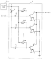
携帯電話等の無線通信機器に用いられる増幅器には、通常2〜3個の高周波増幅用の化合物半導体トランジスタを多段接続した構成が用いられており、この化合物半導体トランジスタとして、近年は単一正電源動作等の観点からヘテロ接合バイポーラトランジスタが主に用いられている。出力電力が1〜3W程度の携帯電話用増幅器の最終段用の増幅器としては、高周波特性及び高出力を確保するため、複数のトランジスタを並列接続させて、各トランジスタの出力を合成させる構成が用いられる。図10は、この構成による従来の高周波電力増幅器100の構成例を示す図である(特許文献1及び特許文献2を参照)。
An amplifier used in a wireless communication device such as a cellular phone usually has a configuration in which two to three compound semiconductor transistors for high-frequency amplification are connected in multiple stages. Heterojunction bipolar transistors are mainly used from the viewpoint of operation and the like. As a final stage amplifier of a mobile phone amplifier having an output power of about 1 to 3 W, a configuration in which a plurality of transistors are connected in parallel and the outputs of the transistors are combined in order to ensure high frequency characteristics and high output is used. It is done. FIG. 10 is a diagram showing a configuration example of a conventional high-
図10に示す従来の高周波電力増幅器100において、バイアス回路Biasから与えられる直流のバイアス電圧DCは、それぞれの抵抗Ra101〜Ra10nを介して各トランジスタTR101〜TR10nのベース(B)に供給される。また、交流信号である高周波信号RFは、それぞれの容量C101〜C10nを介して各トランジスタTR101〜TR10nのベースに入力される。このように、バイアス電圧DCと高周波信号RFとを、別の経路でトランジスタTR101〜TR10nのベースに入力する構成にするのは、以下の理由によるものである。
In the conventional high-
トランジスタTR101〜TR10nは、高出力動作をするとき、交流電流の電流密度が高くなるため発熱する。この発熱は、トランジスタTR101〜TR10n間の特性ばらつき等の要因により、全てのトランジスタTR101〜TR10nにおいて均一ではない。このため、温度が高い特定のトランジスタは、動作時の多大な発熱量で熱暴走し、ベース電流の増大による素子破壊を引き起こす恐れがある。そこで、この熱暴走を抑制するため、トランジスタTR101〜TR10nのベース電圧が上昇したら、バイアス回路Biasから供給されるベースバイアス電流が少なくなるように、抵抗Ra101〜Ra10nの値を大きくすることが考えられる。
上述した従来の高周波電力増幅器100では、抵抗Ra101〜Ra10nの値を大きくすることによって、トランジスタTR101〜TR10nの熱暴走を抑え、かつ、均一動作を実現させている。
In the conventional high-
しかしながら、この抵抗Ra101〜Ra10nの高抵抗化は、高周波信号にとって電力利得低下の原因となるため、あまり大きな値をとることができない。すなわち、抵抗Ra101〜Ra10nの値を大きくすることで改善されるトランジスタTR101〜TR10nの均一動作の確保(耐破壊性の向上)と、抵抗Ra101〜Ra10nの値を小さくすることで向上できるトランジスタTR101〜TR10nの高周波電力利得(高周波特性の向上)とは、トレードオフの関係があり、これらを両立させることは非常に困難であった。 However, the increase in resistance of the resistors Ra101 to Ra10n causes a decrease in power gain for high-frequency signals, and cannot take a very large value. That is, ensuring the uniform operation of the transistors TR101 to TR10n (improving the breakdown resistance) improved by increasing the values of the resistors Ra101 to Ra10n, and improving the transistors TR101 to TR10n by decreasing the values of the resistors Ra101 to Ra10n There is a trade-off relationship with the high-frequency power gain (improvement of high-frequency characteristics) of TR10n, and it has been very difficult to achieve both.
それ故に、本発明の目的は、十分な耐破壊性と良好な高周波特性とを両立させた高周波電力増幅器を提供することである。 SUMMARY OF THE INVENTION Therefore, an object of the present invention is to provide a high frequency power amplifier that achieves both sufficient destruction resistance and good high frequency characteristics.
本発明は、高周波信号の電力増幅に用いられる高周波電力増幅器に向けられている。そして、上記目的を達成させるために、本発明の高周波電力増幅器は、並列接続されたエミッタ接地の複数のトランジスタ、一方端子に直流バイアス電圧が共通印加されかつ他方端子が複数のトランジスタのベースにそれぞれ接続される複数の抵抗、一方電極に高周波信号が共通入力されかつ他方電極が複数のトランジスタのベースにそれぞれ接続される複数の容量、及び複数の抵抗の一方端子と複数の容量の一方電極とを接続する少なくとも1つのブリッジ抵抗とを備えている。 The present invention is directed to a high frequency power amplifier used for power amplification of a high frequency signal. In order to achieve the above object, the high-frequency power amplifier of the present invention includes a plurality of transistors connected in parallel with a common emitter, a DC bias voltage commonly applied to one terminal, and the other terminal connected to the bases of the plurality of transistors. A plurality of resistors connected, a plurality of capacitors each having a high-frequency signal commonly input to one electrode and the other electrode connected to the bases of the plurality of transistors, and one terminal of the plurality of resistors and one electrode of the plurality of capacitors And at least one bridge resistor to be connected.
なお、容量は複数である必要はなく、1つの容量を介して高周波信号を複数のトランジスタのベースに入力してもよい。また、ブリッジ抵抗は、複数の抵抗に対応して複数設けてもよい。また、典型的には、直流バイアス電圧が、エミッタフォロアを出力構成に用いたバイアス回路から供給される。 Note that there is no need for a plurality of capacitors, and a high-frequency signal may be input to the bases of a plurality of transistors through one capacitor. A plurality of bridge resistors may be provided corresponding to a plurality of resistors. Typically, a DC bias voltage is supplied from a bias circuit using an emitter follower as an output configuration.
好ましくは、複数の抵抗の他方端子及び1つ又は複数の容量の他方電極の接続点と複数のトランジスタのベースとの間に、複数の第2抵抗がそれぞれ挿入される。又は、1つ又は複数の容量の他方電極と複数のトランジスタのベースとの間に、複数の第2抵抗がそれぞれ挿入される。あるいは、ブリッジ抵抗の高周波信号が入力される端子と1つ又は複数の容量の一方電極との間に、1つ又は複数の第2抵抗がそれぞれ挿入される。この場合、第2抵抗を伝送線路で形成してもよい。 Preferably, a plurality of second resistors are respectively inserted between the connection points of the other terminals of the plurality of resistors and the other electrode of the one or more capacitors and the bases of the plurality of transistors. Alternatively, a plurality of second resistors are inserted between the other electrode of the one or more capacitors and the bases of the plurality of transistors, respectively. Alternatively, one or more second resistors are respectively inserted between a terminal to which a high frequency signal of the bridge resistor is input and one electrode of one or more capacitors. In this case, the second resistor may be formed of a transmission line.
本発明によれば、複数のトランジスタが並列接続された構成の高周波電力増幅器において、1つ又は複数のブリッジ抵抗を挿入することにより、十分な耐破壊性と良好な高周波特性とを両立させることができる。 According to the present invention, in a high-frequency power amplifier having a configuration in which a plurality of transistors are connected in parallel, by inserting one or more bridge resistors, it is possible to achieve both sufficient breakdown resistance and good high-frequency characteristics. it can.
[第1の実施形態]
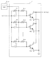
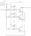
図1は、本発明の第1の実施形態に係る高周波電力増幅器1の回路構成を示す図である。図1において、第1の実施形態に係る高周波電力増幅器1は、トランジスタTR1〜TRnと、容量C1〜Cnと、抵抗Ra1〜Ranと、ブリッジ抵抗Rとで構成される。但し、nは2以上の整数である。トランジスタTR1〜TRnには、化合物半導体(InGaP)を用いたヘテロ接合バイポーラトランジスタに限らず、Si又はSiGeを用いた他のトランジスタを使用することが可能である。
[First Embodiment]
FIG. 1 is a diagram showing a circuit configuration of a high-
交流信号である高周波信号RFは、容量C1〜Cnを介してトランジスタTR1〜TRnのベース(B)にそれぞれ入力され、増幅されてトランジスタTR1〜TRnのコレクタ(C)から出力される。各トランジスタTR1〜TRnのエミッタ(E)は、接地されている。バイアス回路Biasから与えられる直流のバイアス電圧DCは、抵抗Ra1〜Ranを介してトランジスタTR1〜TRnのベースにそれぞれ供給される。このバイアス電圧DCの信号線は、ブリッジ抵抗Rを介して高周波信号RFの入力線と直流的に接続されている。なお、バイアス回路Biasは、バイアス電圧DCを供給できる回路であればその構成は特に問わない。 The high-frequency signal RF, which is an AC signal, is input to the bases (B) of the transistors TR1 to TRn via the capacitors C1 to Cn, amplified, and output from the collectors (C) of the transistors TR1 to TRn. The emitters (E) of the transistors TR1 to TRn are grounded. A direct bias voltage DC supplied from the bias circuit Bias is supplied to the bases of the transistors TR1 to TRn via the resistors Ra1 to Ran, respectively. The signal line of the bias voltage DC is connected to the input line of the high frequency signal RF via the bridge resistor R in a direct current manner. The configuration of the bias circuit Bias is not particularly limited as long as it can supply the bias voltage DC.
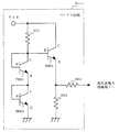
例えば、好ましいバイアス回路Biasとして、図2に示すエミッタフォロア回路が考えられる。図2のバイアス回路Biasは、エミッタフォロアとなるトランジスタTRB3と、温度特性を補償するための抵抗RB1と、バイアス回路特性を補正するための抵抗RB2及びRB3と、トランジスタTRB1及びTRB2とで構成される。トランジスタTRB1及びTRB2は、トランジスタTR1〜TRnとトランジスタTRB3とのベース−エミッタ間電圧和を補償するために、ベース−コレクタ間をショートしてベース−エミッタ間ダイオードとして用いられている。なお、抵抗RB2及びRB3は省略可能である。 For example, an emitter follower circuit shown in FIG. 2 can be considered as a preferable bias circuit Bias. The bias circuit Bias in FIG. 2 includes a transistor TRB3 serving as an emitter follower, a resistor RB1 for compensating temperature characteristics, resistors RB2 and RB3 for correcting bias circuit characteristics, and transistors TRB1 and TRB2. . The transistors TRB1 and TRB2 are used as base-emitter diodes by shorting the base-collector to compensate for the base-emitter voltage sum of the transistors TR1-TRn and the transistor TRB3. The resistors RB2 and RB3 can be omitted.
次に、上記構成による第1の実施形態に係る高周波電力増幅器1の動作を説明する。
ブリッジ抵抗Rの挿入によって、高周波信号RFは、従来の容量C1〜Cnを通過する経路に加えて、ブリッジ抵抗R及び抵抗Ra1〜Ranを通過する経路によっても、トランジスタTR1〜TRnのベースに入力される。このブリッジ抵抗R及び抵抗Ra1〜Ranを通過する経路によって、ブリッジ抵抗Rを介して、高周波信号RFがバイアス回路Bias側に入力されることになる。
Next, the operation of the high-
By inserting the bridge resistor R, the high-frequency signal RF is input to the bases of the transistors TR1 to TRn not only through the path through the conventional capacitors C1 to Cn but also through the path through the bridge resistor R and the resistors Ra1 to Ran. The The high-frequency signal RF is input to the bias circuit Bias side via the bridge resistor R through a path that passes through the bridge resistor R and the resistors Ra1 to Ran.
バイアス回路Bias側に入力される高周波信号RFの電圧振幅は、トランジスタTRB3のベース−エミッタ間ダイオードの非線形性により、トランジスタTRB3のベース−エミッタ間ダイオードをオンするタイミング(負振幅)ではクリップされ、オフするタイミング(正振幅)ではクリップされない。このため、ブリッジ抵抗Rと抵抗Ra1〜Ranとの接続点Pに、正極性の直流オフセット電圧が発生する。この直流オフセット電圧発生の効果は、高周波信号RFの入力電力が大きくなればなるほど顕著に現れる。 The voltage amplitude of the high-frequency signal RF input to the bias circuit Bias is clipped at the timing of turning on the base-emitter diode of the transistor TRB3 (negative amplitude) due to the nonlinearity of the base-emitter diode of the transistor TRB3, and off. It is not clipped at the timing (positive amplitude). For this reason, a positive DC offset voltage is generated at the connection point P between the bridge resistor R and the resistors Ra1 to Ran. The effect of generating the DC offset voltage becomes more prominent as the input power of the high-frequency signal RF increases.
図3A及び図3Bを参照して、第1の実施形態に係る高周波電力増幅器1と従来の高周波電力増幅器100(図10)との効果の違いを説明する。
図3Aは、ブリッジ抵抗Rが25Ω又は50Ωである場合において、抵抗Ra1〜Ranを可変した時の出力電力Poutを示す図である。図3Bは、ブリッジ抵抗Rが25Ω又は50Ωである場合において、抵抗Ra1〜Ranを可変した時の電力負荷効率PAEを示す図である。図からわかるように、従来の高周波電力増幅器100では、抵抗値=1000Ωを超えたあたりから急激に特性が劣化しているのに対し、第1の実施形態に係る高周波電力増幅器1では、抵抗値=2000Ω付近においても殆ど特性劣化が見られない。2000Ω付近では、出力電力Poutで約1.5dB、電力負荷効率PAEで約10%と、大幅な特性改善が可能であることが示されている。
With reference to FIG. 3A and FIG. 3B, the difference in the effect of the high
FIG. 3A is a diagram showing the output power Pout when the resistances Ra1 to Ran are varied when the bridge resistance R is 25Ω or 50Ω. FIG. 3B is a diagram illustrating the power load efficiency PAE when the resistances Ra1 to Ran are varied when the bridge resistance R is 25Ω or 50Ω. As can be seen from the figure, in the conventional high-
このように大幅な特性改善が得られる理由は、ブリッジ抵抗Rと抵抗Ra1〜Ranとの接続点Pにおける電位上昇が、抵抗Ra1〜Ranでの電圧降下を補償しているためである。また、さらに注目すべきは、接続点Pの電位上昇を、トランジスタTR1〜TRn動作の均一性を改善するための抵抗Ra1〜Ranの値を大きくすることに利用できている点である。 The reason why such a significant characteristic improvement is obtained is that the potential increase at the connection point P between the bridge resistor R and the resistors Ra1 to Ran compensates for the voltage drop at the resistors Ra1 to Ran. Further, it should be noted that the potential increase at the connection point P can be used to increase the values of the resistors Ra1 to Ran for improving the uniformity of the operation of the transistors TR1 to TRn.
以上のように、本発明の第1の実施形態に係る高周波電力増幅器1によれば、ブリッジ抵抗Rを挿入することにより、十分な耐破壊性と良好な高周波特性とを両立させることができる。
As described above, according to the high-
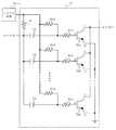
なお、この第1の実施形態では、ブリッジ抵抗Rを1つ挿入する例を説明したが、図4に示すようにトランジスタTR1〜TRn毎にブリッジ抵抗R1〜Rnを挿入した構成の高周波電力増幅器1’でも、同様の効果を得ることができる。また、図5に示すように、複数の容量C1〜Cnが1つの容量Cにまとめられた構成の高周波電力増幅器1''でも、同様の効果を得ることができる。
In the first embodiment, an example in which one bridge resistor R is inserted has been described. However, as shown in FIG. 4, the high-
[第2の実施形態]
図6は、本発明の第2の実施形態に係る高周波電力増幅器2の回路構成を示す図である。図6において、第2の実施形態に係る高周波電力増幅器2は、トランジスタTR1〜TRnと、容量C1〜Cnと、抵抗Ra1〜Ranと、抵抗Rb1〜Rbnと、ブリッジ抵抗Rとで構成される。図6でわかるように、第2の実施形態に係る高周波電力増幅器2は、第1の実施形態に係る高周波電力増幅器1に抵抗Rb1〜Rbnを加えた構成である。
[Second Embodiment]
FIG. 6 is a diagram showing a circuit configuration of the high-
各抵抗Rb1〜Rbnは、微小な抵抗値をとり、容量C1〜Cnと抵抗Ra1〜Ranとの接続点と、トランジスタTR1〜TRnのベースとの間に、それぞれ挿入される。よって、この抵抗Rb1〜Rbnは、トランジスタTR1〜TRnのベースバラスト抵抗として機能する。 Each of the resistors Rb1 to Rbn has a very small resistance value, and is inserted between a connection point between the capacitors C1 to Cn and the resistors Ra1 to Ran and the bases of the transistors TR1 to TRn. Therefore, the resistors Rb1 to Rbn function as base ballast resistors for the transistors TR1 to TRn.
以上のように、本発明の第2の実施形態に係る高周波電力増幅器2によれば、トランジスタTR1〜TRnのベースに微小な抵抗Rb1〜Rbnを挿入することにより、上記第1の実施形態による効果に加えて、トランジスタTR1〜TRnの安定化及び不要発振の抑制が実現可能となる。また、図4に示した複数のブリッジ抵抗R1〜Rnを挿入する構成や図5に示した単一の容量Cを有する構成に、第2の実施形態を応用することも勿論可能である。
As described above, according to the high
[第3の実施形態]
図7は、本発明の第3の実施形態に係る高周波電力増幅器3の回路構成を示す図である。図7において、第3の実施形態に係る高周波電力増幅器3は、トランジスタTR1〜TRnと、容量C1〜Cnと、抵抗Ra1〜Ranと、抵抗Rc1〜Rcnと、ブリッジ抵抗Rとで構成される。図7でわかるように、第3の実施形態に係る高周波電力増幅器3は、第1の実施形態に係る高周波電力増幅器1に抵抗Rc1〜Rcnを加えた構成である。
[Third Embodiment]
FIG. 7 is a diagram showing a circuit configuration of the high-frequency power amplifier 3 according to the third embodiment of the present invention. In FIG. 7, the high-frequency power amplifier 3 according to the third embodiment includes transistors TR1 to TRn, capacitors C1 to Cn, resistors Ra1 to Ran, resistors Rc1 to Rcn, and a bridge resistor R. As can be seen from FIG. 7, the high-frequency power amplifier 3 according to the third embodiment has a configuration in which resistors Rc1 to Rcn are added to the high-
各抵抗Rc1〜Rcnは、微小な抵抗値をとり、容量C1〜Cnと、抵抗Ra1〜RanとトランジスタTR1〜TRnのベースとの接続点との間に、それぞれ挿入される。よって、この抵抗Rc1〜Rcnは、トランジスタTR1〜TRnのベースバラスト抵抗として機能する。 Each of the resistors Rc1 to Rcn has a very small resistance value, and is inserted between the capacitors C1 to Cn and a connection point between the resistors Ra1 to Ran and the bases of the transistors TR1 to TRn. Accordingly, the resistors Rc1 to Rcn function as base ballast resistors for the transistors TR1 to TRn.
以上のように、本発明の第3の実施形態に係る高周波電力増幅器3によれば、トランジスタTR1〜TRnのベースに微小な抵抗Rc1〜Rcnを接続することにより、上記第1の実施形態による効果に加えて、トランジスタTR1〜TRnの安定化及び不要発振の抑制が実現可能となる。また、図4に示した複数のブリッジ抵抗R1〜Rnを挿入する構成や図5に示した単一の容量Cを有する構成に、第3の実施形態を応用することも勿論可能である。 As described above, according to the high frequency power amplifier 3 according to the third embodiment of the present invention, by connecting the small resistors Rc1 to Rcn to the bases of the transistors TR1 to TRn, the effect of the first embodiment can be obtained. In addition, stabilization of the transistors TR1 to TRn and suppression of unnecessary oscillation can be realized. Further, it is of course possible to apply the third embodiment to a configuration in which a plurality of bridge resistors R1 to Rn shown in FIG. 4 are inserted and a configuration having a single capacitor C shown in FIG.
[第4の実施形態]
図8は、本発明の第4の実施形態に係る高周波電力増幅器4の回路構成を示す図である。図8において、第4の実施形態に係る高周波電力増幅器4は、トランジスタTR1〜TRnと、容量C1〜Cnと、抵抗Ra1〜Ranと、伝送線路TL1〜TLnと、ブリッジ抵抗Rとで構成される。図8でわかるように、第4の実施形態に係る高周波電力増幅器4は、第1の実施形態に係る高周波電力増幅器1に伝送線路TL1〜TLnを加えた構成である。
[Fourth Embodiment]
FIG. 8 is a diagram showing a circuit configuration of the high-
各伝送線路TL1〜TLnは、高周波信号RFの入力端子と、容量C1〜Cnとの間に、それぞれ挿入される。この伝送線路TL1〜TLnは、高周波電力増幅器の回路を半導体チップ上に実際にレイアウトした場合に、素子間の配線によって発生する抵抗成分である。この伝送線路TL1〜TLnによって、容量C1〜Cnとの自己共振を生じさせ、高周波信号RFの入力端子とトランジスタTR1〜TRnのベースとの間のインピーダンスが小さくなる。よって、高周波信号RFが通り易くなるので、電力利得等の高周波特性の改善が可能になる。なお、伝送線路TL1〜TLnに代えて一般的な抵抗を用いても構わない。 Each transmission line TL1 to TLn is inserted between the input terminal of the high frequency signal RF and the capacitors C1 to Cn. The transmission lines TL1 to TLn are resistance components generated by wiring between elements when the circuit of the high frequency power amplifier is actually laid out on a semiconductor chip. The transmission lines TL1 to TLn cause self-resonance with the capacitors C1 to Cn, and the impedance between the input terminal of the high frequency signal RF and the bases of the transistors TR1 to TRn is reduced. Therefore, since the high-frequency signal RF can be easily passed, it is possible to improve high-frequency characteristics such as power gain. A general resistor may be used instead of the transmission lines TL1 to TLn.
以上のように、本発明の第4の実施形態に係る高周波電力増幅器4によれば、伝送線路TL1〜TLnを有効に活用することにより、高周波特性のさらなる改善が可能である。また、同一の高周波特性で良ければ、容量C1〜Cnの面積を小さくすることができ、チップサイズの小型化に貢献できる。また、図4に示した複数のブリッジ抵抗R1〜Rnを挿入する構成や図5に示した単一の容量Cを有する構成に、第4の実施形態を応用することも勿論可能である。
As described above, according to the high-
[第5の実施形態]
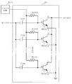
図9は、本発明の第5の実施形態に係る高周波電力増幅器5の回路構成を示す図である。図9において、第5の実施形態に係る高周波電力増幅器5は、増幅器50〜52、複数のコレクタバイアス回路53、複数のバイアス回路55、入力整合回路56、第1の段間整合回路57、第2の段間整合回路58及び出力整合回路59を備える。
[Fifth Embodiment]
FIG. 9 is a diagram showing a circuit configuration of the high-frequency power amplifier 5 according to the fifth embodiment of the present invention. In FIG. 9, the high-frequency power amplifier 5 according to the fifth embodiment includes
増幅器50〜52には、上述した第1〜第3の実施形態に係る高周波電力増幅器1〜3のいずれかの構成が用いられる。増幅器50〜52に接続される複数のバイアス回路55は、例えば上記第1の実施形態で説明したバイアス回路Biasである。コレクタバイアス回路53は、伝送線路(例えばλ/4線路)やインダクタやキャパシタからなり、トランジスタTR1〜TRnのコレクタにバイアスを供給する。入力整合回路56、第1の段間整合回路57、第2の段間整合回路58及び出力整合回路59は、インピーダンスの異なるトランジスタをインピーダンス整合させ、かつ、高周波特性を引き出すための回路であり、伝送線路、インダクタ又はキャパシタから構成される。
Any of the configurations of the high-
このような複数段構成の高周波電力増幅器5においても、本発明の高周波電力増幅器1〜3を適用させることで、十分な耐破壊性と良好な高周波特性とを両立させることができる。特に、各増幅段での特性誤差を最小にさせることができるので、入力電力とバイアス電圧との関係を適切に調整することにより、増幅器の線形性を改善した低歪増幅器への適用も可能となる。
Even in such a high-frequency power amplifier 5 having a multi-stage configuration, by applying the high-
本発明の高周波電力増幅器は、携帯電話等の無線通信機器に用いられる増幅器として利用可能であり、特に十分な耐破壊性と良好な高周波特性とを両立させたい場合等に適している。 The high-frequency power amplifier of the present invention can be used as an amplifier used in a wireless communication device such as a mobile phone, and is particularly suitable when it is desired to achieve both sufficient breakdown resistance and good high-frequency characteristics.
1〜5、1’、1''、100 高周波電力増幅器
50〜52 増幅器
53 コレクタバイアス回路
55、Bias バイアス回路
56〜59 整合回路
C、C1〜Cn、C101〜C10n 容量
R、R1〜Rn、Ra1〜Ran、Rb1〜Rbn、Rc1〜Rcn、RB1〜RB3、Ra101〜Ra10n 抵抗
TL1〜TLn 伝送線路
TR1〜TRn、TRB1〜TRB3、TR101〜TR10n トランジスタ
Vdd 電源
1-5, 1 ′, 1 ″, 100 RF power amplifier 50-52
Claims (11)
並列接続されたエミッタ接地の複数のトランジスタと、
一方端子に直流バイアス電圧が共通印加され、他方端子が前記複数のトランジスタのベースにそれぞれ接続される複数の抵抗と、
一方電極に前記高周波信号が共通入力され、他方電極が前記複数のトランジスタのベースにそれぞれ接続される複数の容量と、
前記複数の抵抗の一方端子と前記複数の容量の一方電極とを接続する少なくとも1つのブリッジ抵抗とを備える、高周波電力増幅器。 A high frequency power amplifier used for power amplification of a high frequency signal,
A plurality of grounded emitter transistors connected in parallel;
A plurality of resistors each having a DC bias voltage commonly applied to one terminal and the other terminal connected to the bases of the plurality of transistors;
A plurality of capacitors in which the high-frequency signal is commonly input to one electrode and the other electrode is connected to the bases of the plurality of transistors;
A high frequency power amplifier comprising: at least one bridge resistor connecting one terminal of the plurality of resistors and one electrode of the plurality of capacitors.
並列接続されたエミッタ接地の複数のトランジスタと、
一方端子に直流バイアス電圧が共通印加され、他方端子が前記複数のトランジスタのベースにそれぞれ接続される複数の抵抗と、
一方電極に前記高周波信号が入力され、他方電極が前記複数のトランジスタのベースに接続される容量と、
前記複数の抵抗の一方端子と前記容量の一方電極とを接続する少なくとも1つのブリッジ抵抗とを備える、高周波電力増幅器。 A high frequency power amplifier used for power amplification of a high frequency signal,
A plurality of grounded emitter transistors connected in parallel;
A plurality of resistors each having a DC bias voltage commonly applied to one terminal and the other terminal connected to the bases of the plurality of transistors;
A capacitor in which the high-frequency signal is input to one electrode and the other electrode is connected to bases of the plurality of transistors;
A high frequency power amplifier comprising: at least one bridge resistor connecting one terminal of the plurality of resistors and one electrode of the capacitor.
Priority Applications (5)
| Application Number | Priority Date | Filing Date | Title |
|---|---|---|---|
| JP2005148103A JP2006325096A (en) | 2005-05-20 | 2005-05-20 | High-frequency power amplifier |
| US11/435,891 US7449957B2 (en) | 2005-05-20 | 2006-05-18 | Radio frequency power amplifier |
| DE602006016892T DE602006016892D1 (en) | 2005-05-20 | 2006-05-19 | RF power amplifiers |
| EP06010419A EP1727278B1 (en) | 2005-05-20 | 2006-05-19 | Radio frequency power amplifier |
| CN200610084725A CN100593902C (en) | 2005-05-20 | 2006-05-19 | Radio frequency power amplifier |
Applications Claiming Priority (1)
| Application Number | Priority Date | Filing Date | Title |
|---|---|---|---|
| JP2005148103A JP2006325096A (en) | 2005-05-20 | 2005-05-20 | High-frequency power amplifier |
Publications (2)
| Publication Number | Publication Date |
|---|---|
| JP2006325096A true JP2006325096A (en) | 2006-11-30 |
| JP2006325096A5 JP2006325096A5 (en) | 2008-06-26 |
Family
ID=36709591
Family Applications (1)
| Application Number | Title | Priority Date | Filing Date |
|---|---|---|---|
| JP2005148103A Pending JP2006325096A (en) | 2005-05-20 | 2005-05-20 | High-frequency power amplifier |
Country Status (5)
| Country | Link |
|---|---|
| US (1) | US7449957B2 (en) |
| EP (1) | EP1727278B1 (en) |
| JP (1) | JP2006325096A (en) |
| CN (1) | CN100593902C (en) |
| DE (1) | DE602006016892D1 (en) |
Cited By (3)
| Publication number | Priority date | Publication date | Assignee | Title |
|---|---|---|---|---|
| JP2009260639A (en) * | 2008-04-16 | 2009-11-05 | Mitsubishi Electric Corp | High frequency amplifier |
| JP2011155482A (en) * | 2010-01-27 | 2011-08-11 | Tdk Corp | Power amplifier |
| JP2012119794A (en) * | 2010-11-29 | 2012-06-21 | Sumitomo Electric Ind Ltd | Electronic circuit |
Families Citing this family (16)
| Publication number | Priority date | Publication date | Assignee | Title |
|---|---|---|---|---|
| JP2007300159A (en) * | 2006-04-27 | 2007-11-15 | Sharp Corp | Circuit unit, power supply bias circuit, lnb, and transmitter |
| US7598809B2 (en) * | 2007-11-30 | 2009-10-06 | Silicon Storage Technology, Inc. | RF power amplifier |
| JP2010124433A (en) * | 2008-11-21 | 2010-06-03 | Panasonic Corp | High-frequency power amplifier |
| CN101656514B (en) * | 2009-09-07 | 2011-09-28 | 东南大学 | Gain controllable parallel radio-frequency power amplifier based on matching share |
| CN101847967A (en) * | 2010-05-31 | 2010-09-29 | 锐迪科科技有限公司 | Radio-frequency power amplifier circuit |
| CN101876834B (en) * | 2010-06-23 | 2014-03-12 | 中兴通讯股份有限公司 | Tracking power supply device and control method thereof |
| KR101444520B1 (en) * | 2012-02-09 | 2014-09-24 | 삼성전기주식회사 | Amplifier circuit and operating method thereof |
| CN103326675A (en) * | 2013-06-21 | 2013-09-25 | 苏州广帝科微电子有限公司 | Linear radiofrequency power amplifier |
| JP2017183839A (en) * | 2016-03-28 | 2017-10-05 | 株式会社村田製作所 | Power amplifier circuit |
| US10873296B2 (en) | 2016-12-30 | 2020-12-22 | Richwave Technology Corp. | Amplifier device |
| TWI664806B (en) * | 2016-12-30 | 2019-07-01 | 立積電子股份有限公司 | Amplifier device |
| EP3346608B1 (en) * | 2017-01-09 | 2021-05-26 | Nxp B.V. | Rf amplifier |
| JP2019129402A (en) * | 2018-01-24 | 2019-08-01 | 株式会社村田製作所 | Distortion compensation circuit |
| CN108599729A (en) * | 2018-06-25 | 2018-09-28 | 浙江大学 | Increase power amplifier output power to drive the circuit structure of transmitting transducer |
| CN111277227A (en) * | 2020-03-18 | 2020-06-12 | 锐石创芯(深圳)科技有限公司 | Co-emitting and co-based amplifying circuit for improving phase characteristics and signal processing system |
| CN114142818A (en) * | 2021-10-14 | 2022-03-04 | 深圳飞骧科技股份有限公司 | Radio frequency power amplifier applied to 5G-Sub6G frequency band communication system |
Citations (7)
| Publication number | Priority date | Publication date | Assignee | Title |
|---|---|---|---|---|
| JP2001127071A (en) * | 1999-08-19 | 2001-05-11 | Hitachi Ltd | Semiconductor device and its manufacturing method |
| JP2001196865A (en) * | 1999-10-29 | 2001-07-19 | Hitachi Ltd | Wireless communication apparatus and semiconductor device |
| JP2001274636A (en) * | 2000-03-28 | 2001-10-05 | Toshiba Corp | High frequency power amplifier using bipolar transistor |
| JP2003264438A (en) * | 2002-03-08 | 2003-09-19 | Murata Mfg Co Ltd | High frequency power amplifier |
| JP2003283274A (en) * | 2002-03-27 | 2003-10-03 | Matsushita Electric Ind Co Ltd | High frequency power amplifier |
| JP2003324325A (en) * | 2002-02-27 | 2003-11-14 | Sharp Corp | Power amplifier |
| JP2004080763A (en) * | 2002-07-23 | 2004-03-11 | Mediatek Inc | Power amplifier integrated circuit |
Family Cites Families (11)
| Publication number | Priority date | Publication date | Assignee | Title |
|---|---|---|---|---|
| JPH0427349A (en) | 1990-05-22 | 1992-01-30 | Sanyo Electric Co Ltd | Apparatus for producing frozen food |
| US5321279A (en) | 1992-11-09 | 1994-06-14 | Texas Instruments Incorporated | Base ballasting |
| US5608353A (en) | 1995-03-29 | 1997-03-04 | Rf Micro Devices, Inc. | HBT power amplifier |
| JP2001274639A (en) * | 2000-03-27 | 2001-10-05 | Toshiba Corp | Semiconductor power amplifier and multi-stage monolithic integrated circuit |
| JP2002217378A (en) | 2001-01-19 | 2002-08-02 | Toshiba Corp | High-frequency power amplifier |
| US6538515B2 (en) * | 2001-01-19 | 2003-03-25 | Telefonaktiebolaget Lm Ericsson (Publ) | Power amplifier and method of operating a power amplifier having multiple output-power modes |
| US6750721B2 (en) * | 2002-04-30 | 2004-06-15 | Freescale Semiconductor, Inc. | HBT linearizer and power booster |
| US6653902B1 (en) | 2002-09-03 | 2003-11-25 | Triquint Semiconductor, Inc. | Amplifier power control circuit |
| US6727761B1 (en) * | 2002-09-03 | 2004-04-27 | Triquint Semiconductor, Inc. | Resonant bypassed base ballast circuit |
| JP2004194063A (en) | 2002-12-12 | 2004-07-08 | Renesas Technology Corp | High-frequency power amplifier and communication apparatus using the same |
| JP2005295057A (en) * | 2004-03-31 | 2005-10-20 | Matsushita Electric Ind Co Ltd | Power amplifier |
-
2005
- 2005-05-20 JP JP2005148103A patent/JP2006325096A/en active Pending
-
2006
- 2006-05-18 US US11/435,891 patent/US7449957B2/en not_active Expired - Fee Related
- 2006-05-19 EP EP06010419A patent/EP1727278B1/en not_active Expired - Fee Related
- 2006-05-19 CN CN200610084725A patent/CN100593902C/en not_active Expired - Fee Related
- 2006-05-19 DE DE602006016892T patent/DE602006016892D1/en active Active
Patent Citations (7)
| Publication number | Priority date | Publication date | Assignee | Title |
|---|---|---|---|---|
| JP2001127071A (en) * | 1999-08-19 | 2001-05-11 | Hitachi Ltd | Semiconductor device and its manufacturing method |
| JP2001196865A (en) * | 1999-10-29 | 2001-07-19 | Hitachi Ltd | Wireless communication apparatus and semiconductor device |
| JP2001274636A (en) * | 2000-03-28 | 2001-10-05 | Toshiba Corp | High frequency power amplifier using bipolar transistor |
| JP2003324325A (en) * | 2002-02-27 | 2003-11-14 | Sharp Corp | Power amplifier |
| JP2003264438A (en) * | 2002-03-08 | 2003-09-19 | Murata Mfg Co Ltd | High frequency power amplifier |
| JP2003283274A (en) * | 2002-03-27 | 2003-10-03 | Matsushita Electric Ind Co Ltd | High frequency power amplifier |
| JP2004080763A (en) * | 2002-07-23 | 2004-03-11 | Mediatek Inc | Power amplifier integrated circuit |
Cited By (3)
| Publication number | Priority date | Publication date | Assignee | Title |
|---|---|---|---|---|
| JP2009260639A (en) * | 2008-04-16 | 2009-11-05 | Mitsubishi Electric Corp | High frequency amplifier |
| JP2011155482A (en) * | 2010-01-27 | 2011-08-11 | Tdk Corp | Power amplifier |
| JP2012119794A (en) * | 2010-11-29 | 2012-06-21 | Sumitomo Electric Ind Ltd | Electronic circuit |
Also Published As
| Publication number | Publication date |
|---|---|
| US20060261897A1 (en) | 2006-11-23 |
| EP1727278B1 (en) | 2010-09-15 |
| CN100593902C (en) | 2010-03-10 |
| US7449957B2 (en) | 2008-11-11 |
| CN1866729A (en) | 2006-11-22 |
| DE602006016892D1 (en) | 2010-10-28 |
| EP1727278A1 (en) | 2006-11-29 |
Similar Documents
| Publication | Publication Date | Title |
|---|---|---|
| JP2006325096A (en) | High-frequency power amplifier | |
| US7834700B2 (en) | Radio frequency power amplifier | |
| US7439805B1 (en) | Enhancement-depletion Darlington device | |
| US10355653B2 (en) | Power amplifier circuit | |
| US8497736B1 (en) | Direct DC coupled push-pull BJT driver for power amplifier with built-in gain and bias current signal dependent expansion | |
| US7692493B1 (en) | High-efficiency single to differential amplifier | |
| TW201545470A (en) | Improved power amplifier bias circuit having parallel emitter follower | |
| JP5234006B2 (en) | Power amplifier | |
| JP3556469B2 (en) | Active low-pass filter | |
| KR20120125811A (en) | Power amplifier | |
| JP2004194063A (en) | High-frequency power amplifier and communication apparatus using the same | |
| WO2004112244A1 (en) | High-frequency amplifier | |
| US20050083128A1 (en) | [power amplifier with active bias circuit] | |
| US20060145760A1 (en) | High efficiency linear RF amplifier | |
| US20050140439A1 (en) | Predistortion linearizer for power amplifier | |
| JP2011010245A (en) | High-frequency power amplifier | |
| JP2007243872A (en) | Transistor circuit and high-frequency amplifier using the same | |
| KR100591062B1 (en) | Linear power amplifier for predistortion by using reverse diode | |
| JP2008124559A (en) | Power amplifier and communication device employing the same | |
| US11190151B2 (en) | Power amplifier | |
| KR20130061614A (en) | Power amplifier | |
| US20060261888A1 (en) | Amplifier arrangement | |
| US20230141220A1 (en) | Power amplifier circuit | |
| Cijvat et al. | A GaN HEMT power amplifier with variable gate bias for envelope and phase signals | |
| JP2005184258A (en) | High-frequency amplifier |
Legal Events
| Date | Code | Title | Description |
|---|---|---|---|
| A521 | Request for written amendment filed |
Free format text: JAPANESE INTERMEDIATE CODE: A523 Effective date: 20080514 |
|
| A621 | Written request for application examination |
Free format text: JAPANESE INTERMEDIATE CODE: A621 Effective date: 20080514 |
|
| A977 | Report on retrieval |
Free format text: JAPANESE INTERMEDIATE CODE: A971007 Effective date: 20100408 |
|
| A131 | Notification of reasons for refusal |
Free format text: JAPANESE INTERMEDIATE CODE: A131 Effective date: 20100412 |
|
| A521 | Request for written amendment filed |
Free format text: JAPANESE INTERMEDIATE CODE: A523 Effective date: 20100526 |
|
| A02 | Decision of refusal |
Free format text: JAPANESE INTERMEDIATE CODE: A02 Effective date: 20101224 |