JP2006324344A - Semiconductor device and manufacturing method thereof - Google Patents
Semiconductor device and manufacturing method thereof Download PDFInfo
- Publication number
- JP2006324344A JP2006324344A JP2005144387A JP2005144387A JP2006324344A JP 2006324344 A JP2006324344 A JP 2006324344A JP 2005144387 A JP2005144387 A JP 2005144387A JP 2005144387 A JP2005144387 A JP 2005144387A JP 2006324344 A JP2006324344 A JP 2006324344A
- Authority
- JP
- Japan
- Prior art keywords
- well
- oxide film
- semiconductor device
- film
- type well
- Prior art date
- Legal status (The legal status is an assumption and is not a legal conclusion. Google has not performed a legal analysis and makes no representation as to the accuracy of the status listed.)
- Pending
Links
Images
Landscapes
- Element Separation (AREA)
- Metal-Oxide And Bipolar Metal-Oxide Semiconductor Integrated Circuits (AREA)
Abstract
【課題】 CMOS半導体装置において、反転領域対策を、CMOS半導体装置の製造工程を変えないで実現することを課題とする。
【解決手段】 境界領域40については、p形ウェル203とn形ウェル202の境界5の部分の上に、第1層酸化膜208とポリシリコン膜210−2aと第3層酸化膜214とが重なっており、この第3層酸化膜214の上面に、n形ウェル202から延在しているアルミニウム配線216Aが形成してある構造である。p形ウェル203及びn形ウェル202からアルミニウム配線8までの離間距離はL2であり、従来の離間距離L1に比べて長い。ポリシリコン膜210−2aはゲートを形成するために形成されたポリシリコン膜210−1の除去されずに残された部分である。
【選択図】 図1PROBLEM TO BE SOLVED: To realize an inversion region countermeasure in a CMOS semiconductor device without changing the manufacturing process of the CMOS semiconductor device.
In the boundary region 40, a first layer oxide film 208, a polysilicon film 210-2a, and a third layer oxide film 214 are formed on the boundary 5 portion of the p-type well 203 and the n-type well 202. In this structure, an aluminum wiring 216A extending from the n-type well 202 is formed on the upper surface of the third layer oxide film 214. The separation distance from the p-type well 203 and the n-type well 202 to the aluminum wiring 8 is L2, which is longer than the conventional separation distance L1. The polysilicon film 210-2a is a portion left without being removed of the polysilicon film 210-1 formed to form the gate.
[Selection] Figure 1
Description
本発明は半導体装置及びその製造方法に係り、特に、Nチャネル型MOSとPチャネル型MOSとが隣り合って密接して配置している部分の改良に関する。 The present invention relates to a semiconductor device and a method for manufacturing the same, and more particularly to an improvement in a portion where an N channel type MOS and a P channel type MOS are arranged close to each other.
一般的に、CMOS半導体装置はシリコン基板にNチャネル型MOSとPチャネル型MOSとが隣り合って密接して配置して作り込んで形成してある。 In general, a CMOS semiconductor device is formed by forming an N channel type MOS and a P channel type MOS in close contact with each other on a silicon substrate.
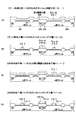
図8は従来のCMOS半導体装置1のNチャネル型MOS20とPチャネル型MOS30とが隣接している境界の部分を示す。40は境界領域である。2はp形のシリコン基板、3はp形ウェル、4はn形ウェルである。5はp形ウェル3とn形ウェル4との境界である。6は第1層酸化膜であり、7は第3層酸化膜である。8はアルミニウム配線であり、nウェル4側から出て延在して隣接しているnウェル4とpウェル3との境界の部分に沿っており、一部は、pウェル3の上側に張り出ている。
FIG. 8 shows a boundary portion where the N-
n形ウェル4は境界領域40の隣りの部位がVddに接続してあり、p形ウェル3は境界領域40の隣りの部位がGndに接続してあり、この境界領域40は反転領域10が形成され易い部分である。
The n-
境界領域40については、p形ウェル3とn形ウェル4との境界5の部分の上に、第1層酸化膜6と第3層酸化膜7とが重なっており、この第3層酸化膜7の上面にアルミニウム配線8が形成してある構造である。p形ウェル3及びn形ウェル4からアルミニウム配線8までの離間距離はL1である。
For the
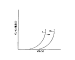
この離間距離L1が反転電圧を決定する一つの要因である。反転電圧とは、アルミニウム配線8に印加する電圧を上昇させていった場合に、アルミニウム配線8から発生する電界によってp形ウェル3のうちアルミニウム配線8の真下に当る部分に電子が集まってきて、反転領域10が形成されるときの電圧である。反転電圧が高い程、反転領域が形成され難くなる。なお、反転領域10はp形ウェル3のうちアルミニウム配線8の真下に当る部分、即ち、p形ウェル3のうちn形ウェル4との境界の近傍に形成される。
p形ウェル3の端の部分に反転領域10が形成されると、反転領域10を通ってPチャネル型MOS30からNチャネル型MOS20へ電流が流れ、これが原因で、Nチャネル型MOS20のV−I特性が、図3中、本来の線Iで示す状態から、線IAで示すようにシフトし特性が低下してしまう。
When the
近年、CMOS半導体装置においては各素子が緻密になって集積度も更に高くなる傾向にある。このようになると、各素子のレイアウトが制約を受けて、nウェル側から出て延在するアルミニウム配線のうちには、nウェルとpウェルとの境界の部分に沿うものが多くなる傾向となる。このことは一つの半導体チップのうちに形成される可能性のある反転領域の数が多くなることを意味し、よって、将来的に、反転領域対策は重要な課題である。 In recent years, in a CMOS semiconductor device, each element tends to be dense and the degree of integration tends to be further increased. In this case, the layout of each element is restricted, and among the aluminum wirings extending out from the n-well side, those along the boundary portion between the n-well and the p-well tend to increase. . This means that the number of inversion regions that can be formed in one semiconductor chip increases, and therefore inversion region countermeasures will be an important issue in the future.
なお、反転電圧を上げるための構造は、CMOS半導体装置の現在の製造の工程、条件を変えないで達成できることが重要である。生産現場において、反転電圧を上げるためだけに、製造の工程、条件を変えることは現実的でないからである。よって、前記の例において、反転電圧を上げるために、第1層酸化膜6と第3層酸化膜7の厚さを厚くすることも考えられるけれども、第1層酸化膜6と第3層酸化膜7の厚さを厚くすると、成膜の条件及び成膜した酸化膜をエッチングするための条件等を設定し直すことが必要となり、解決手段として好ましくない。
It is important that the structure for increasing the inversion voltage can be achieved without changing the current manufacturing process and conditions of the CMOS semiconductor device. This is because it is not practical to change the manufacturing process and conditions only in order to increase the reverse voltage at the production site. Therefore, in the above example, the first
そこで、本発明は、上記課題を解決した半導体装置及びその製造方法を提供することを目的とする。 In view of the above, an object of the present invention is to provide a semiconductor device and a method for manufacturing the same that solve the above-described problems.
本発明は、基板に複数の半導体素子が集積して形成してあり、該基板を覆う酸化膜を有し、且つ、該酸化膜の上面に金属配線を有する構成の半導体装置において、
該基板に形成されて隣接しているnウェルとpウェルとの境界に対応する部分については、前記半導体素子を形成する工程の途中で形成した膜(210−2a)が残してあり、
前記pウェルと、前記nウェル側から出て延在して前記隣接しているnウェルとpウェルとの境界の部分を通っている金属配線との間に、前記酸化膜と前記残された膜とを有する構成としたことを特徴とする。
The present invention provides a semiconductor device having a structure in which a plurality of semiconductor elements are integrated on a substrate, an oxide film covering the substrate, and a metal wiring on the upper surface of the oxide film.
A film (210-2a) formed in the middle of the process of forming the semiconductor element remains in the portion corresponding to the boundary between the n well and the p well formed adjacent to each other on the substrate,
The oxide film is left between the p-well and the metal wiring extending from the n-well side and passing through the boundary portion between the adjacent n-well and p-well. It has the structure which has a film | membrane.
本発明によれば、半導体装置の製造設備を変えないで、且つ、各工程の作業の条件も変更しないで、反転領域対策を備えた構造を実現することが可能となる。 According to the present invention, it is possible to realize a structure with an inversion region countermeasure without changing the semiconductor device manufacturing equipment and without changing the work conditions of each process.
次に本発明の実施の形態について説明する。 Next, an embodiment of the present invention will be described.
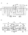
図1(A),(B)は本発明の実施例1になるCMOS半導体装置1Aのうち、隣接しているNチャネル型MOS20とPチャネル型MOS30との部分を示す。図1(A)は平面図、図1(B)は同図(A)中、線IB−IBに沿う断面図である。図2はNチャネル型MOS20とPチャネル型MOS30との境界領域40を拡大して且つ簡略的に示す図であり、図8に対応する図である。
1A and 1B show adjacent N-
p形のシリコン基板2の表面には、多数のNチャネル型MOS20とPチャネル型MOS30とが密接して作り込まれている。
A large number of N-
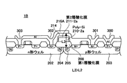
境界領域40については、p形ウェル203とn形ウェル202の境界5の部分の上に、第1層酸化膜208とポリシリコン膜210−2aと第3層酸化膜214とが重なっており、この第3層酸化膜214の上面に多数本のアルミニウム配線216が形成してある構造である。ここで、p形ウェル203とn形ウェル202の境界5の部分とは、境界5、及びn形ウェル202のうち境界5に沿う部分、及びp形ウェル203のうち境界5に沿う部分を含めた帯状の部分をいう。多数本のアルミニウム配線216のうちアルミニウム配線216Aは、nウェル202側から出て延在して隣接しているnウェル202とpウェル203との境界の部分を通っている。図1(A)中、円41で囲んで示す部分は、アルミニウム配線216Aのうちp形ウェル203上に張り出している部分を示す。p形ウェル203のうちこの円41で囲んだ部分に対応する部分に反転領域が形成される可能性がある。
For the
ここで、ポリシリコン膜210−2aが存在することによって、p形ウェル203及びn形ウェル202からアルミニウム配線216Aまでの離間距離はL2であり、図8に示す従来のCMOS半導体装置1の離間距離L1に比べて長い。よって、反転電圧は従来に比較して高く、反転領域が形成され難く、Nチャネル型MOS20は図3中、線Iで示す本来の特性を有する。
Here, due to the presence of the polysilicon film 210-2a, the separation distance from the p-
ポリシリコン膜210−2aはCMOS半導体装置1Aを製造する工程の一つでシリコン基板2の全面に形成されたポリシリコン膜210−1のうち、除去されずに残されたものである。
The polysilicon film 210-2a is one that is left without being removed from the polysilicon film 210-1 formed on the entire surface of the
次に、上記構造のCMOS半導体装置1Aの製造工程について説明する。
Next, a manufacturing process of the
図4はCMOS半導体装置1Aの製造工程図である。CMOS半導体装置1Aは、酸化工程101からn形ウェル形成工程102、p形ウェル形成工程103、nC/S(nMOSチャネルストッパー)形成工程104、pC/S(pMOSチャネルストッパー)形成工程105、窒化膜形成工程106、第1層酸化膜形成工程108、ゲート酸化工程109、ゲート形成工程110、SWS(Side Wall Spacer)形成工程111、nS/D(nMOSソース、ドレイン)形成工程112、pS/D(pMOSソース、ドレイン)形成工程113、第3層酸化膜形成工程114、電極用孔形成工程115、アルミニウム配線形成工程116を経て、窒化膜形成工程117までの工程を経て製造される。
FIG. 4 is a manufacturing process diagram of the
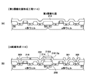
ゲート形成工程110は、ポリシリコン成膜工程110−1とフォトエッチング工程110−2とよりなる。SWS形成工程111は、第2層酸化膜形成工程111−1とフォトエッチング工程111−2とよりなる。 The gate forming step 110 includes a polysilicon film forming step 110-1 and a photoetching step 110-2. The SWS formation step 111 includes a second layer oxide film formation step 111-1 and a photoetching step 111-2.
図5(A)はポリシリコン成膜工程110−1が完了したときの状態を示す。図5(B)はフォトエッチング工程110−2が完了したときの状態を示す。 FIG. 5A shows a state when the polysilicon film forming step 110-1 is completed. FIG. 5B shows a state when the photoetching step 110-2 is completed.
図5(C)は第2層酸化膜形成工程111−1が完了したときの状態を示す。図5(D)はフォトエッチング工程111−2が完了したときの状態を示す。 FIG. 5C shows a state when the second layer oxide film forming step 111-1 is completed. FIG. 5D shows a state when the photoetching step 111-2 is completed.
図6(A)は第3層酸化膜形成工程114が完了したときの状態を示す。 FIG. 6A shows the state when the third layer oxide film forming step 114 is completed.
図6(B)はアルミニウム配線形成工程116が完了したときの状態を示す。 FIG. 6B shows a state when the aluminum wiring forming step 116 is completed.
図5及び図6において、各工程によって形成された部分は、200番台の符号であって、1番台及び10番台については工程を示す符号と同じ符号を付す。 5 and 6, the part formed by each process is a code in the 200s, and the same codes as the codes indicating the processes are given to the 1st and 10s.
シリコン基板2が、酸化工程101、n形ウェル形成工程102、p形ウェル形成工程103、nC/S(nMOSチャネルストッパー)形成工程104、pC/S(pMOSチャネルストッパー)形成工程105、窒化膜形成工程106、第1層酸化膜形成工程108、ゲート酸化工程109、ポリシリコン成膜工程110−1を経ると、図5(A)に示す状態となる。境界領域40については、n形ウェル202とp形ウェル203との境界5の部分の上に、第1層酸化膜208が形成されている。ポリシリコン膜210−1は本来はゲートを作るためのものであり基板2の全面に形成してある。また、このポリシリコン膜210−1には不純物を添加しない。
The
次のポリシリコン膜210−1をエッチングするフォトエッチング工程110−2では、従来とは異なるパターンのマスク、即ち、第1層酸化膜208上のポリシリコン膜も追加して残すパターンのマスクを用いる。フォトエッチング工程110−2が完了すると、図5(B)に示すように、n形ウェル202とp形ウェル203上にポリシリコン膜210−2が残されると共に、第1層酸化膜208上にポリシリコン膜210−2aが残された状態となる。残されたポリシリコン膜210−2の部位にゲートが形成される。残されたポリシリコン膜210−2aは前記の離間距離L2を稼ぐ。
In the next photoetching step 110-2 for etching the polysilicon film 210-1, a mask having a pattern different from the conventional one, that is, a mask having a pattern in which the polysilicon film on the
次いで、第2層酸化膜形成工程111−1が行われ、図5(C)に示すように、基板2の全面に第2層酸化膜211−1が形成される。この第2層酸化膜211−1はSWSを形成するために形成される。
Next, a second layer oxide film forming step 111-1 is performed, and a second layer oxide film 211-1 is formed on the entire surface of the
次いで、フォトエッチング工程111−2が行われ、図5(D)に示すように、ポリシリコン膜210−1の周囲とポリシリコン膜210−2aの周囲とにだけに第2層酸化膜211−2が残されてSWSが形成される。ここで、境界領域40の部分の第1層酸化膜208の上面はポリシリコン膜210−2aによって覆われているため、第2層酸化膜211−1をフォトエッチングして除去するときに、境界領域40の部分の第1層酸化膜208の上面がフォトエッチングされてしまって、境界領域40の部分の第1層酸化膜208が無用に薄くなってしまうことは起きない。このことも、前記の離間距離L2を稼ぐように作用する。
Next, a photoetching step 111-2 is performed, and as shown in FIG. 5D, the second layer oxide film 211- is formed only around the polysilicon film 210-1 and around the polysilicon film 210-2a. 2 is left to form the SWS. Here, since the upper surface of the first
次いで、nS/D(nMOSソース、ドレイン)形成工程112、pS/D(pMOSソース、ドレイン)形成工程113が行われて、nS/D(nMOSソース、ドレイン)212及びpS/D213(pMOSソース、ドレイン)が形成される(図6(A)参照)。 Next, an nS / D (nMOS source, drain) forming step 112 and a pS / D (pMOS source, drain) forming step 113 are performed, and an nS / D (nMOS source, drain) 212 and a pS / D213 (pMOS source, drain) are performed. A drain) is formed (see FIG. 6A).
次いで、第3層酸化膜形成工程114が行われ、図6(A)に示すように、全面に第3層酸化膜214が形成される。
Next, a third layer oxide film forming step 114 is performed, and a third
次いで、電極用孔形成工程115がなされ第3層酸化膜214に孔が形成され、更に、アルミニウム配線形成工程116が行われて、図6(B)示すように、アルミニウム配線216、216A及びバックゲート電極300、ソース電極301、バックゲート電極302、ソース電極303が形成される。最後に、窒化膜形成工程117が行われて、窒化膜が形成され、CMOS半導体装置1Aが完成する。
Next, an electrode
上記の工程101から工程117は、工程110−2で使用するマスクを除いて、図8に示す従来のCMOS半導体装置1を製造する工程と全く同じである。よって、CMOS半導体装置1Aは、CMOS半導体装置1を製造する設備を使用し、且つ、各設備の設定条件も変えないで稼動させて製造することが出来る。
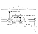
図7は本発明の実施例2になるCMOS半導体装置1Bのうち、隣接しているNチャネル型MOS20とPチャネル型MOS30との部分を示す。
FIG. 7 shows adjacent N-
図1に示すCMOS半導体装置1Aと相違する点は、p形ウェル203とn形ウェル202との境界5の部分と、アルミニウム配線216Aとの間に、第1層酸化膜208とポリシリコン膜210−2aと第3層酸化膜214に加えて、第2層酸化膜211−2aが加わっている点である。この第2層酸化膜211−2aは、第2層酸化膜211−1の一部であって除去されずに残されたものであり、ポリシリコン膜210−2aの上面に形成されている。
1 differs from the
p形ウェル3及びn形ウェル4からアルミニウム配線216Aまでの離間距離はL3であり、図1に示すCMOS半導体装置1Aにおける離間距離L2よりも長く、反転電圧は更に高くなる。
The separation distance from the p-type well 3 and the n-type well 4 to the
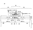
1A,1B CMOS半導体装置
5 境界
20 Nチャネル型MOS
30 Pチャネル型MOS
40 境界領域
202 n形ウェル
203 p形ウェル
208 第1層酸化膜
210−2a 残されたポリシリコン膜
211−2a 残された第2層酸化膜
214 第3層酸化膜
216A、216 アルミニウム配線
1A, 1B
30 P-channel MOS
40 boundary region 202 n-type well 203 p-type well 208 first layer oxide film 210-2a remaining polysilicon film 211-2a remaining second
Claims (4)
該基板に形成されて隣接しているnウェルとpウェルとの境界に対応する部分については、前記半導体素子を形成する工程の途中で形成した膜が残してあり、
前記pウェルと、前記nウェル側から出て延在して前記隣接しているnウェルとpウェルとの境界の部分を通っている金属配線との間に、前記酸化膜と前記残された膜とを有する構成としたことを特徴とする半導体装置。 In a semiconductor device having a structure in which a plurality of semiconductor elements are integrated and formed on a substrate, an oxide film covering the substrate, and a metal wiring on the upper surface of the oxide film,
For the portion corresponding to the boundary between the adjacent n well and p well formed on the substrate, the film formed in the middle of the process of forming the semiconductor element remains,
The oxide film is left between the p-well and the metal wiring extending from the n-well side and passing through the boundary portion between the adjacent n-well and p-well. A semiconductor device comprising a film.
前記半導体素子はCMOSであり、
前記残された膜は、該CMOSのゲートを形成するために前記基板の全面に形成されたポリシリコン膜のうちの残されたポリシリコン膜であることを特徴とする半導体装置。 The semiconductor device according to claim 1,
The semiconductor element is a CMOS,
2. The semiconductor device according to claim 1, wherein the remaining film is a remaining polysilicon film among the polysilicon films formed on the entire surface of the substrate in order to form the gate of the CMOS.
前記半導体素子はCMOSであり、
前記残された膜は、該CMOSのゲートを形成するために前記基板の全面に形成されたポリシリコン膜のうちの残されたポリシリコン膜と、
該ゲートのサイドウォールスペーサを形成するために前記基板の全面に形成されて別の酸化膜のうちの残されたの別の酸化膜とよりなり、
残されたポリシリコン膜と該残されたの別の酸化膜とが重なっている構成であることを特徴とする半導体装置。 The semiconductor device according to claim 1,
The semiconductor element is a CMOS,
The remaining film is a remaining polysilicon film among the polysilicon films formed on the entire surface of the substrate to form the CMOS gate;
In order to form the side wall spacer of the gate, it is formed on the entire surface of the substrate and is formed of another oxide film remaining among the other oxide films,
A semiconductor device characterized in that a remaining polysilicon film and another remaining oxide film overlap each other.
半導体素子を形成する工程の途中で前記酸化膜の全面を覆うように形成された膜のうち、隣接しているnウェルとpウェルとの境界に対応する部分については、残すように処理する工程と、
前記nウェル側から出て延在して前記隣接しているnウェルとpウェルとの境界の部分を通る金属配線を形成する工程とよりなることを特徴とする半導体装置の製造方法。 forming an oxide film so as to cover a substrate in which an n-well and a p-well are formed adjacent to each other;
Of the film formed so as to cover the entire surface of the oxide film during the process of forming the semiconductor element, the process corresponding to the boundary between the adjacent n-well and p-well is left so as to remain When,
And a step of forming a metal wiring extending from the n-well side and passing through a boundary portion between the adjacent n-well and p-well.
Priority Applications (1)
| Application Number | Priority Date | Filing Date | Title |
|---|---|---|---|
| JP2005144387A JP2006324344A (en) | 2005-05-17 | 2005-05-17 | Semiconductor device and manufacturing method thereof |
Applications Claiming Priority (1)
| Application Number | Priority Date | Filing Date | Title |
|---|---|---|---|
| JP2005144387A JP2006324344A (en) | 2005-05-17 | 2005-05-17 | Semiconductor device and manufacturing method thereof |
Publications (1)
| Publication Number | Publication Date |
|---|---|
| JP2006324344A true JP2006324344A (en) | 2006-11-30 |
Family
ID=37543817
Family Applications (1)
| Application Number | Title | Priority Date | Filing Date |
|---|---|---|---|
| JP2005144387A Pending JP2006324344A (en) | 2005-05-17 | 2005-05-17 | Semiconductor device and manufacturing method thereof |
Country Status (1)
| Country | Link |
|---|---|
| JP (1) | JP2006324344A (en) |
-
2005
- 2005-05-17 JP JP2005144387A patent/JP2006324344A/en active Pending
Similar Documents
| Publication | Publication Date | Title |
|---|---|---|
| US8354316B2 (en) | Reduced mask configuration for power mosfets with electrostatic discharge (ESD) circuit protection | |
| US6858885B2 (en) | Semiconductor apparatus and protection circuit | |
| US9831271B2 (en) | Semiconductor device | |
| US8003461B1 (en) | Method of fabricating efuse structure, resistor sturcture and transistor sturcture | |
| US20120258592A1 (en) | Layouts of POLY Cut Openings Overlapping Active Regions | |
| JP4991134B2 (en) | Semiconductor device and manufacturing method thereof | |
| JP2005142321A (en) | Semiconductor integrated circuit device and manufacturing method thereof | |
| US7410874B2 (en) | Method of integrating triple gate oxide thickness | |
| JP5501668B2 (en) | Semiconductor device manufacturing method, semiconductor chip, and semiconductor wafer | |
| JP4533804B2 (en) | Semiconductor device and manufacturing method thereof | |
| JP3380836B2 (en) | MIS semiconductor device and method of manufacturing the same | |
| JP2006324344A (en) | Semiconductor device and manufacturing method thereof | |
| JP4426996B2 (en) | Semiconductor device and manufacturing method of semiconductor device | |
| JP4947964B2 (en) | Semiconductor device and manufacturing method thereof | |
| JP2007194562A (en) | Semiconductor device and manufacturing method thereof | |
| KR20020096055A (en) | 2-input NOR Gate comprising NMOS tansistor and PMOS transistor formed on different semiconductor layers | |
| JP5163212B2 (en) | Semiconductor device and manufacturing method thereof | |
| JP2010245432A (en) | Semiconductor device | |
| JPH0677442A (en) | Method for manufacturing semiconductor integrated circuit | |
| JP2005175214A (en) | Semiconductor device and manufacturing method thereof | |
| KR0147776B1 (en) | How to Connect Sea Mode Inverter | |
| JPH03256356A (en) | Semiconductor device | |
| KR100843015B1 (en) | Isolation Method of Semiconductor Devices | |
| JP2007335463A (en) | Electrostatic discharging protective element, and semiconductor device | |
| JP2013084656A (en) | Semiconductor device |