JP2006190853A - Quantum well structure and its manufacturing method - Google Patents
Quantum well structure and its manufacturing method Download PDFInfo
- Publication number
- JP2006190853A JP2006190853A JP2005002072A JP2005002072A JP2006190853A JP 2006190853 A JP2006190853 A JP 2006190853A JP 2005002072 A JP2005002072 A JP 2005002072A JP 2005002072 A JP2005002072 A JP 2005002072A JP 2006190853 A JP2006190853 A JP 2006190853A
- Authority
- JP
- Japan
- Prior art keywords
- layer
- quantum well
- well layer
- well structure
- growth
- Prior art date
- Legal status (The legal status is an assumption and is not a legal conclusion. Google has not performed a legal analysis and makes no representation as to the accuracy of the status listed.)
- Granted
Links
Images

Abstract
Description
本発明は、圧縮歪みの大きな井戸層を有する良質な量子井戸構造及び当該構造を容易に製造することができる製造方法に関し、例えば、半導体レーザ、光変調素子および光増幅素子などの活性層に用いることができる。 The present invention relates to a high-quality quantum well structure having a well layer having a large compressive strain and a manufacturing method capable of easily manufacturing the structure, for example, for use in active layers such as semiconductor lasers, light modulation elements, and light amplification elements. be able to.
従来、圧縮歪を加えた井戸層を有する歪量子井戸構造を、半導体レーザの活性層として用いることによって、発振しきい値電流の低減、発振スペクトル線幅の狭線幅化および変調周波数の高速化など、レーザ特性が著しく改善されることが、数多く報告されている。 Conventionally, by using a strained quantum well structure having a well layer with compressive strain as the active layer of a semiconductor laser, the oscillation threshold current is reduced, the oscillation spectral line width is narrowed, and the modulation frequency is increased. It has been reported that laser characteristics are remarkably improved.
井戸層の圧縮歪量をさらに増大させることができれば、オージェ再結合による非発光再結合の低減効果や微分利得の増大効果によって、発振しきい電流や変調周波数等におけるレーザ特性がさらに向上することが知られている(下記、非特許文献1,2を参照)。
If the amount of compressive strain in the well layer can be further increased, the laser characteristics at the oscillation threshold current, modulation frequency, etc. can be further improved by the effect of reducing non-radiative recombination by Auger recombination and the effect of increasing differential gain. Known (see
基板上にInGaAsあるいはInGaAsPを成長させる場合、結晶成長の進行が層状となる、いわゆる2次元成長がデバイス形成のための結晶成長の前提になっているが、基板と成長層との格子定数の差、すなわち歪量が大きい場合、結晶成長の進行が島状となる、いわゆる3次元成長となることが知られている。成長層の圧縮歪を増加させた場合、結晶成長が2次元成長から3次元成長に変わる歪量は+1.5%程度であることが知られている(下記、非特許文献3を参照。)。 When growing InGaAs or InGaAsP on a substrate, so-called two-dimensional growth in which the progress of crystal growth is layered is a prerequisite for crystal growth for device formation, but the difference in lattice constant between the substrate and the growth layer That is, when the amount of strain is large, it is known that the progress of crystal growth becomes island-like, so-called three-dimensional growth. When the compressive strain of the growth layer is increased, it is known that the amount of strain at which crystal growth changes from two-dimensional growth to three-dimensional growth is about + 1.5% (see Non-Patent Document 3 below). .
また、上記圧縮歪を有するInGaAsあるいはInGaAsP井戸層の3次元成長には、III族原料であるインジウムの表面拡散(マイグレーション)が大きく影響していることが知られている(下記、非特許文献4を参照。)。
In addition, it is known that the surface diffusion (migration) of indium, which is a group III material, greatly affects the three-dimensional growth of an InGaAs or InGaAsP well layer having the compressive strain (see Non-Patent
通常、基板に格子整合したInGaAsあるいはInGaAsPを成長させる場合、良質な結晶性を得るために、インジウムの表面拡散を促し、表面拡散長を長くすることが望ましい。しかし、成長させるInGaAsあるいはInGaAsPが基板に対し圧縮歪を有する場合、インジウムの拡散長が長いと、3次元成長の基点となる膜中の欠陥や転位に到達するインジウム数が増加するため、3次元成長が起こりやすい。 Normally, when growing InGaAs or InGaAsP lattice-matched to a substrate, it is desirable to promote the surface diffusion of indium and increase the surface diffusion length in order to obtain good crystallinity. However, when the InGaAs or InGaAsP to be grown has a compressive strain with respect to the substrate, if the indium diffusion length is long, the number of indiums reaching the defects and dislocations in the film that becomes the base point of the three-dimensional growth increases. Growth is likely to occur.
基板上に圧縮歪を有するInGaAsあるいはInGaAsPを井戸層とする歪多重量子井戸構造を成長させる場合においても、井戸層が上述するように大きな圧縮歪を有すると、上記3次元成長の影響によって、非発光再結合中心となる欠陥が発生するなどの問題が生ずる。 Even in the case of growing a strained multiple quantum well structure having InGaAs or InGaAsP having compressive strain on a substrate as a well layer, if the well layer has a large compressive strain as described above, non- Problems such as the occurrence of defects that become luminescent recombination centers occur.
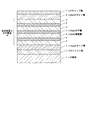
図4は、従来方法により作製された歪多重量子井戸構造を示す概略断面構造図である。
同図には、大きな圧縮歪を有する井戸層を含む歪多重量子井戸構造において、3次元成長が発生した場合の断面を模式的に示してある。
FIG. 4 is a schematic sectional view showing a strained multiple quantum well structure manufactured by a conventional method.
This figure schematically shows a cross section when three-dimensional growth occurs in a strained multiple quantum well structure including a well layer having a large compressive strain.
同図に示すように、従来の歪多重量子井戸構造20はInGaAsP障壁層14とInGaAs井戸層15とが積層されてなり、歪多重量子井戸構造20の一方には、InP基板11とInPバッファ層12とInGaAsPガイド層13とが形成され、他方にはInGaAsPガイド層16とInPキャップ層17とが形成されている。一例として、障壁層14を4層とし、井戸層15は3層とした例を示してある。
As shown in the figure, the conventional strained multiple
このような井戸層15の3次元成長は、井戸層15の圧縮歪が大きくなるほど顕著になることが知られている。さらに、井戸層15の積層数が増大すると、それに伴って歪多重量子井戸構造20内に蓄積される歪応力が増加するため、上記3次元成長の影響が増大することが知られている(下記、非特許文献5を参照。)。
It is known that such three-dimensional growth of the
したがって、歪量が+1.5%以上の井戸層を有する歪量子井戸構造において、欠陥の発生を抑え、良質な結晶を得るためには、上記3次元成長を抑制する必要があった。 Therefore, in the strained quantum well structure having a well layer having a strain amount of + 1.5% or more, it is necessary to suppress the three-dimensional growth in order to suppress the generation of defects and obtain a high-quality crystal.
また、井戸層の圧縮歪を増加させるためには、InGaAsあるいはInGaAsPにおけるインジウム組成を増加させる必要がある。しかし、InGaAsあるいはInGaAsP中のインジウム組成の増加によりInGaAsあるいはInGaAsP表面にインジウム組成の大きな領域(インジウムリッチ領域)が生じる。さらに上記インジウムリッチ領域に形成されたInGaAsからインジウムが再蒸発するため、InGaAsにおけるインジウム組成が減少し、インジウム組成の大きなInGaAs、すなわち大きな圧縮歪を有するInGaAsが成長できないことが知られている(下記、非特許文献6を参照。)。 In order to increase the compressive strain of the well layer, it is necessary to increase the indium composition in InGaAs or InGaAsP. However, an increase in the indium composition in InGaAs or InGaAsP causes a region having a large indium composition (indium rich region) on the surface of InGaAs or InGaAsP. Further, it is known that indium is re-evaporated from InGaAs formed in the indium-rich region, so that the indium composition in InGaAs is reduced, and InGaAs having a large indium composition, that is, InGaAs having a large compressive strain cannot be grown (see below). , See Non-Patent Document 6.)
したがって、圧縮歪が+1.5%以上の井戸層を有する歪量子井戸構造を得るためには、InGaAsあるいはInGaAsPからのインジウムの再蒸発を抑制する必要もあった。 Therefore, in order to obtain a strained quantum well structure having a well layer with a compressive strain of + 1.5% or more, it has been necessary to suppress re-evaporation of indium from InGaAs or InGaAsP.
上述するように、基板上の歪量子井戸構造における+1.5%以上の圧縮歪を加えたInGaAsあるいはInGaAsPからなる井戸層においては、3次元的な島状成長が発生するという問題があった。さらにインジウムの再蒸発によりInGaAsあるいはInGaAsP中のインジウム組成が減少するため、所望の歪量が得られないという問題があった。 As described above, there is a problem that three-dimensional island-like growth occurs in a well layer made of InGaAs or InGaAsP to which a compressive strain of + 1.5% or more in a strained quantum well structure on a substrate is applied. Furthermore, since the indium composition in InGaAs or InGaAsP is reduced by re-evaporation of indium, there is a problem that a desired amount of strain cannot be obtained.
したがって、歪量子井戸構造を有する半導体レーザ、光変調器素子等の半導体光素子の素子特性を向上させるために、井戸層の3次元成長およびインジウム原子の再蒸発を抑制でき、良質な結晶を得ることができる製造方法が強く求められていた。 Therefore, in order to improve the device characteristics of a semiconductor optical device such as a semiconductor laser having a strained quantum well structure and an optical modulator device, three-dimensional growth of the well layer and re-evaporation of indium atoms can be suppressed, and a high-quality crystal is obtained. There has been a strong demand for a production method that can be used.
本発明は、上記状況に鑑みてなされたものであり、従来技術の問題を解決し、良質な結晶から形成される量子井戸構造及びその製造方法を提供することを目的とする。具体的には、基板と+1.5%以上の歪量を有する井戸層(例えば、InGaAsまたはInGaAsPなどで形成)における3次元成長を抑制することにより、結晶欠陥の発生を抑えることができ、更に、インジウムの再蒸発を抑制することにより、井戸層の歪量を容易に制御した量子井戸構造及びその製造方法を提供することを目的とする。 The present invention has been made in view of the above situation, and an object of the present invention is to solve the problems of the prior art and to provide a quantum well structure formed from high-quality crystals and a method for manufacturing the same. Specifically, the generation of crystal defects can be suppressed by suppressing three-dimensional growth in the well layer (for example, formed of InGaAs or InGaAsP) having a strain amount of + 1.5% or more with the substrate. An object of the present invention is to provide a quantum well structure in which the amount of strain in a well layer is easily controlled by suppressing re-evaporation of indium, and a method for manufacturing the quantum well structure.
上記課題を解決する本発明に係る量子井戸構造は、基板上に形成され、それぞれ格子定数の異なる障壁層と井戸層とを積層してなる量子井戸構造において、3次元成長が抑制されると共に基板の格子定数に対して1.5%以上の圧縮歪を有する井戸層とした量子井戸構造であり、そして、当該特徴を有する構造を実現する製造方法としては、井戸層を成長速度0.4nm/秒以上で形成すること主要な特徴とする。 The quantum well structure according to the present invention that solves the above problems is formed on a substrate, and in a quantum well structure in which a barrier layer and a well layer having different lattice constants are stacked, three-dimensional growth is suppressed and the substrate is suppressed. The quantum well structure is a well layer having a compressive strain of 1.5% or more with respect to the lattice constant, and a manufacturing method for realizing the structure having the characteristic has a growth rate of 0.4 nm / The main feature is to form in seconds or more.
井戸層や障壁層は、例えば、有機金属気相エピタキシー法、分子線エピタキシー法、ガスソース分子線エピタキシー法又は化学ビームエピタキシー法の結晶成長方法で形成することができる。また、井戸層または障壁層は、例えば、それぞれInGaAsまたはInGaAsPにより形成することができる。 The well layer and the barrier layer can be formed by, for example, a crystal growth method such as metal organic vapor phase epitaxy, molecular beam epitaxy, gas source molecular beam epitaxy, or chemical beam epitaxy. Further, the well layer or the barrier layer can be formed of InGaAs or InGaAsP, for example.
一般には、上述するようにInGaAsまたはInGaAsPからなる井戸層の格子歪が+1.5%以上になると3次元的な島状成長が起こり、さらに結晶欠陥が発生するためにデバイスヘの応用が困難であった。また、歪量が+1.5%以上になるとインジウムの再蒸発が顕著になり、インジウム組成を増加させることが困難になるため、井戸層に+1.5%以上の歪量を加えることが困難であった。 In general, as described above, when the lattice strain of a well layer made of InGaAs or InGaAsP becomes + 1.5% or more, three-dimensional island growth occurs, and further crystal defects occur, making it difficult to apply to a device. It was. In addition, when the strain amount is + 1.5% or more, re-evaporation of indium becomes remarkable and it becomes difficult to increase the indium composition. Therefore, it is difficult to apply a strain amount of + 1.5% or more to the well layer. there were.
しかし、第1の実施例に詳細を記載するように、井戸層を成長させる際の成長速度を1秒当たり0.4nm以上にすると、3次元成長を促進させる原因となるインジウムの表面拡散を抑制することができ、InGaAsあるいはInGaAsPからなる井戸層の3次元成長を抑制することができる。その結果、圧縮歪量が増加しても平坦な井戸層と障壁層との界面を有する良質な量子井戸構造とすることができる。 However, as will be described in detail in the first embodiment, when the growth rate when growing the well layer is set to 0.4 nm or more per second, the surface diffusion of indium which causes the three-dimensional growth is suppressed. It is possible to suppress the three-dimensional growth of the well layer made of InGaAs or InGaAsP. As a result, even if the amount of compressive strain increases, a high-quality quantum well structure having an interface between a flat well layer and a barrier layer can be obtained.
さらに、第2の実施例に詳細を記載するように、井戸層を成長させる際の成長速度を1秒当たり0.4nm以上にすることにより、インジウムの再蒸発も抑制可能なため、+1.5%以上の圧縮歪を有するInGaAsあるいはInGaAsPからなる井戸層を有する量子井戸構造においても、井戸層の歪量を容易に制御することができる。 Further, as described in detail in the second embodiment, since the re-evaporation of indium can be suppressed by setting the growth rate when growing the well layer to 0.4 nm or more per second, +1.5 Even in a quantum well structure having a well layer made of InGaAs or InGaAsP having a compressive strain of% or more, the strain amount of the well layer can be easily controlled.
歪量が+1.5%以上の井戸層を有する従来の歪量子井戸構造の製造方法では、井戸層の成長速度に関する規定はなく、特に有機金属気相エピタキシー法(MOVPE法)で井戸層の成長速度により結晶欠陥の発生を抑える方法は取られてこなかった。 In the conventional method for producing a strained quantum well structure having a well layer having a strain amount of + 1.5% or more, there is no regulation regarding the growth rate of the well layer, and the well layer growth is particularly performed by a metal organic vapor phase epitaxy method (MOVPE method). No method has been taken to suppress the generation of crystal defects by speed.
これに対して本発明では、1秒当たりに成長させる膜厚を0.4nm以上とすることで、+1.5%以上の歪量の井戸層を有する量子井戸構造においても、平坦な井戸層と障壁層との界面を有し欠陥の少ない(3次元成長が抑制された)結晶を得ることが可能となる。さらに、井戸層の歪量も容易に制御することが可能となる。なお、成長速度は0.4nm/秒以上であれば、これらの効果を奏すると考えられ、上限値については、現在のところ成膜方法に起因する成膜限界値が上限値となる。したがって、例えば、現在の成膜方法の中でも最も成膜速度が速いと考えられるMOVPE法では、約3nm/秒が上限値となる。しかしながら、当該上限値は成膜方法に起因するものであり、当該上限値以上で上記効果を奏さなくなるという意味ではない。今後、当該上限値以上の成膜性能を有する成膜方法、成膜装置などが開発された場合には、約3nm/秒より速い成膜速度でも上記効果を奏すると考えられる。 On the other hand, in the present invention, by setting the film thickness grown per second to 0.4 nm or more, even in a quantum well structure having a well layer with a strain amount of + 1.5% or more, A crystal having an interface with the barrier layer and few defects (three-dimensional growth is suppressed) can be obtained. Further, the strain amount of the well layer can be easily controlled. If the growth rate is 0.4 nm / second or more, it is considered that these effects can be achieved. As for the upper limit value, the film formation limit value resulting from the film formation method is currently the upper limit value. Therefore, for example, in the MOVPE method, which is considered to have the highest film formation speed among the current film formation methods, the upper limit is about 3 nm / second. However, the upper limit value is attributed to the film forming method, and does not mean that the above effect is not achieved when the upper limit value is exceeded. In the future, when a film forming method, a film forming apparatus or the like having a film forming performance equal to or higher than the upper limit value is developed, it is considered that the above effect can be obtained even at a film forming speed higher than about 3 nm / second.
本発明によれば、従来作製が困難であった+1.5%以上という高い圧縮歪を有し、かつ3次元成長が抑制された井戸層を有する量子井戸構造を容易に作製することができ、当該構造を適用したレーザの高速化、発振しきい値電流の低減などデバイス特性の向上実現に極めて有用である。 According to the present invention, it is possible to easily produce a quantum well structure having a well layer having a high compressive strain of + 1.5% or more, which has been difficult to produce in the past, and having suppressed three-dimensional growth, This structure is extremely useful for improving device characteristics such as increasing the speed of a laser using the structure and reducing the oscillation threshold current.
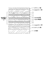
<第1の実施例>
図1は、本発明の実施例に係る歪多重量子井戸構造を示す概略断面構造図である。同図を用いて、井戸層として圧縮歪を有するInGaAsを用い、障壁層としてInGaAsを用いた本発明の第1の実施例を説明する。
<First embodiment>
FIG. 1 is a schematic sectional view showing a strained multiple quantum well structure according to an embodiment of the present invention. The first embodiment of the present invention using InGaAs having compressive strain as the well layer and InGaAs as the barrier layer will be described with reference to FIG.
同図に示すように、本実施例に係る歪多重量子井戸構造10はInGaAs障壁層4とInGaAs井戸層5とを積層してなり、歪多重量子井戸構造10の一方には、InP基板1とInPバッファ層(膜厚200nm)2とInP基板1に格子整合するInGaAsPガイド層(バンドギャップ波長1.3μm、膜厚100nm)3とを形成し、他方にはInP基板1に格子整合するInGaAsPガイド層(バンドギャップ波長1.3μm、膜厚100nm)6とInPキャップ層(膜厚100nm)7とを形成してある。同図には、障壁層4を4層とし、井戸層15は3層とした例を示してある。
As shown in the figure, the strained multiple
InGaAs井戸層5としては圧縮歪を有する膜厚10nmのInGaAs層を用い、InGaAs障壁層4としては引張り歪−0.1%、膜厚18.5nmのInGaAs層を用いた。結晶成長は有機金属気相エピタキシー法によって行い、成長温度は700℃である。また、III族原料としてはトリメチルインジウム(TMIn)およびトリエチルガリウム(TEGa)を用い、V族原料としてはアルシン(AsH3)およびホスフィン(PH3)を使用した。
As the InGaAs well
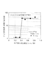
一般に、レーザウエハにおけるフォトルミネッセンス(PL)発光強度は、発振しきい値電流密度と密接な関連があり、フォトルミネッセンス発光強度が低下すると、レーザの発振しきい値電流密度が上昇することが知られている(上記、非特許文献7を参照。)。そのため、良好なデバイス特性を得るためには、井戸層の成長速度をフォトルミネッセンス発光強度の低下が生じない範囲に設定する必要がある。 In general, the photoluminescence (PL) emission intensity in a laser wafer is closely related to the oscillation threshold current density, and it is known that the laser oscillation threshold current density increases as the photoluminescence emission intensity decreases. (See Non-Patent Document 7 above.) Therefore, in order to obtain good device characteristics, it is necessary to set the growth rate of the well layer in a range in which the reduction of the photoluminescence emission intensity does not occur.
図2は、PL(フォトルミネッセンス)発光強度と、井戸層の成長速度(1秒あたりの成長膜厚)との関係の一例を示す図であり、本実施例に係る歪多重量子井戸構造について、フォトルミネッセンス発光強度の井戸層成長速度依存性を測定した結果である。同図では、横軸を井戸層の成長速度(nm/秒)とし、縦軸を歪多重量子井戸構造のフォトルミネッセンス発光強度(対数任意目盛)とした。このときの井戸層の圧縮歪は+1.65%とした。 FIG. 2 is a diagram showing an example of the relationship between PL (photoluminescence) emission intensity and the growth rate of the well layer (growth film thickness per second). Regarding the strained multiple quantum well structure according to this example, FIG. It is the result of measuring the well layer growth rate dependence of photoluminescence luminescence intensity. In the figure, the horizontal axis is the growth rate (nm / second) of the well layer, and the vertical axis is the photoluminescence emission intensity (logarithmic arbitrary scale) of the strained multiple quantum well structure. The compressive strain of the well layer at this time was set to + 1.65%.
同図から明らかなように、フォトルミネッセンス発光強度は、成長速度0.4nm/秒を境に急激に変化し、0.4nm/秒より小さい成長速度では弱い発光強度である一方、0.4nm/秒以上の成長速度では強い発光強度が維持されている。したがって、井戸層5の成長速度を0.4nm/秒以上に設定すれば、フォトルミネッセンス強度の低下を防ぎ、高い発光強度が得られることが確認された。
As is clear from the figure, the photoluminescence emission intensity changes abruptly at a growth rate of 0.4 nm / second, and is weak emission intensity at a growth rate of less than 0.4 nm / second, whereas 0.4 nm / second. Strong light emission intensity is maintained at a growth rate of 2 seconds or more. Therefore, it was confirmed that if the growth rate of the
さらに、InGaAs井戸層5の成長速度を0.68nm/秒として、InGaAs井戸層5の圧縮歪量を増加させて歪多重量子井戸構造10を形成した場合、エックス線回折法(XRD)およびフォトルミネッセンスの観察結果から、3次元成長することなく良質な歪多重量子井戸構造が得られていることが確認された。
Furthermore, when the strain rate of the InGaAs well
一方、成長速度を0.35nm/秒(0.4nm/秒以下)として井戸層を成長させた場合、井戸層が3次元成長してしまうことにより、InGaAs井戸層とInGaAs障壁層における界面が悪化していることがエックス線回折法により磯認された。さらに、フォトルミネッセンス発光は確認できなかった。このように井戸層が3次元成長すると、非発光再結合中心となる欠陥が発生し、フォトルミネッセンスにおける発光強度が著しく低下し、十分な発光強度を得ることは困難である。 On the other hand, when the well layer is grown at a growth rate of 0.35 nm / sec (0.4 nm / sec or less), the interface between the InGaAs well layer and the InGaAs barrier layer deteriorates due to the three-dimensional growth of the well layer. This was confirmed by X-ray diffraction. Furthermore, photoluminescence emission could not be confirmed. When the well layer grows three-dimensionally in this way, defects serving as non-radiative recombination centers are generated, the light emission intensity in photoluminescence is significantly reduced, and it is difficult to obtain sufficient light emission intensity.
しかし、本実施例に示すように、0.4nm/秒以上の成長速度で井戸層5を成長させることにより、井戸層5における3次元成長を抑制でき、その結果として結晶欠陥の発生を抑えることができるため、十分なフォトルミネッセンス発光強度の結晶を得ることができる。
However, as shown in this embodiment, the three-dimensional growth in the
本実施例における検討では井戸層5の成長速度が0.83nm/秒までの場合を示した(図2を参照。)が、0.83nm/秒以上の成長速度においても3次元成長の抑制が可能であり、同様の効果が得られるのは明らかである。
In the study in this example, the case where the growth rate of the
また、本実施例における検討では井戸層5としてInGaAsを用いたが、InGaAsPを井戸層とした場合でも、同様に、井戸層5の成長速度が0.4nm/秒未満では結晶に加わる歪によって3次元成長が生じることが確認された。そして、InGaAsP井戸層の成長速度を本実施例と同様に0.4nm/秒以上とすることによって、本実施例と同様に良好な結果が得られることが確認された。また、本実施例では、障壁層としてInGaAs層を用いたが、InGaAsP層を用いた場合でも本実施例と同様の効果が得られた。
In the study in this example, InGaAs was used as the
また、本実施例ではV族原料としてアルシンおよびホスフィンを用いたが、有機金属材料であるターシャリーブチルアルシン(TBAs)およびターシャリーブチルホスフィン(TBP)を用いても、同様の効果が得られた。 In this example, arsine and phosphine were used as Group V materials, but the same effect was obtained using tertiary butylarsine (TBAs) and tertiary butylphosphine (TBP), which are organometallic materials. .
また、本実施例では有機金属気相エピタキシー法によって各層を成長させたが、分子線エピタキシー法、ガスソース分子線エピタキシー法、化学ビームエピタキシー法のいずれを用いても、同様の効果が得られた。 In this example, each layer was grown by metal organic vapor phase epitaxy, but the same effect was obtained by using any of molecular beam epitaxy, gas source molecular beam epitaxy, and chemical beam epitaxy. .
<第2の実施例>
本実施例に係る歪多重量子井戸構造は、井戸層として圧縮歪を有するInGaAsを用い、障壁層として引張り歪−0.1%を有するInGaAsPを用いると共に、井戸層を3層とし、障壁層を4層とした歪多重量子井戸構造であり、有機金属気相エピタキシー法により成長させて形成した。歪多重量子井戸構造以外の各層部分(InP基板など)は第1の実施例と同じとした。
<Second embodiment>
In the strained multiple quantum well structure according to this example, InGaAs having compressive strain is used as the well layer, InGaAsP having a tensile strain of −0.1% is used as the barrier layer, the well layer has three layers, and the barrier layer has It has a strained multiple quantum well structure with four layers and is grown by metal organic vapor phase epitaxy. Each layer portion (such as an InP substrate) other than the strained multiple quantum well structure is the same as in the first embodiment.
歪多重量子井戸構造の井戸層としては、成長速度を0.35nm/秒(比較例)、0.42nm/秒および0.68nm/秒として成長させた膜厚10nmのInGaAsを用いた。このとき、III族原料であるトリメチルインジウムとトリエチルガリウムの供給量比(III族原料供給量比(TMIn/TEGa))を4から7まで変化させ、井戸層の成長速度を制御して試料をそれぞれ作製した。なお、使用した原料は第1の実施例と同じである。 As a well layer having a strained multiple quantum well structure, InGaAs having a thickness of 10 nm grown at a growth rate of 0.35 nm / second (comparative example), 0.42 nm / second, and 0.68 nm / second was used. At this time, the supply ratio of trimethylindium and triethylgallium, which are Group III materials (Group III material supply ratio (TMIn / TEGa)) is changed from 4 to 7, and the growth rate of the well layer is controlled to control the samples. Produced. The raw materials used are the same as in the first example.
井戸層の成長速度の制御について説明すると、アルシンの流量を一定に保ち、トリメチルインジウム供給量を増加させ、更に、所定のIII族原料供給量比となるようにトリエチルガリウム供給量を調整することにより、成長速度を制御した。すなわち、III族原料供給量比によりインジウム組成を制御(歪量制御)すると共に、アルシンに対するIII族原料供給量により成膜速度を制御した。なお、第1に実施例における成長速度の制御も同様の方法で行っている。 Explaining the control of the growth rate of the well layer, the flow rate of arsine is kept constant, the trimethylindium supply amount is increased, and further, the triethylgallium supply amount is adjusted so as to become a predetermined group III raw material supply amount ratio. , Controlled the growth rate. That is, the indium composition was controlled (strain control) by the group III source supply ratio, and the film formation rate was controlled by the group III source supply to arsine. First, the growth rate in the embodiment is also controlled by the same method.
図3は、井戸層の圧縮歪量と、井戸層成長時におけるトリメチルインジウムとトリエチルガリウムの供給量比との関係の一例を示す図である。同図には、井戸層を成長速度0.35nm/秒、0.42nm/秒および0.68nm/秒で成長させてなる歪多重量子井戸構造についての結果を示してある。 FIG. 3 is a diagram showing an example of the relationship between the amount of compressive strain in the well layer and the supply ratio of trimethylindium and triethylgallium during the growth of the well layer. This figure shows the results for a strained multiple quantum well structure in which a well layer is grown at growth rates of 0.35 nm / second, 0.42 nm / second, and 0.68 nm / second.
基本的に、いずれの成長速度であっても、III族原料供給量比を大きくしてインジウム組成を増加させることで、井戸層の圧縮歪量が増加する傾向となる。しかしながら、井戸層の成長速度を0.35nm/秒とした場合には、圧縮歪量を+1.5%までは増加させることができる一方、+1.5%以上の歪量ではIII族原料供給量比におけるトリメチルインジウムの割合を更に増加させても、圧縮歪量を増加させることができないことが分かる。 Basically, at any growth rate, the amount of compressive strain in the well layer tends to increase by increasing the group III raw material supply amount ratio and increasing the indium composition. However, when the growth rate of the well layer is 0.35 nm / second, the amount of compressive strain can be increased up to + 1.5%, while the amount of strain of + 1.5% or more increases the supply amount of the group III material. It can be seen that even if the ratio of trimethylindium in the ratio is further increased, the amount of compressive strain cannot be increased.
一方、井戸層の成長速度を0.42nm/秒とした場合には、III族原料供給量比が5.6のときに、圧縮歪+1.65%の井戸層を得ることができる。さらに、井戸層の成長速度を0.68nm/秒と増加させた場合には、III族原料供給量比におけるトリメチルインジウムの割合を更に増加させることにより、井戸層の歪量をさらに増加させることが可能であることが確認された。 On the other hand, when the growth rate of the well layer is 0.42 nm / second, a well layer having a compressive strain of + 1.65% can be obtained when the group III raw material supply amount ratio is 5.6. Furthermore, when the growth rate of the well layer is increased to 0.68 nm / second, the strain amount of the well layer can be further increased by further increasing the ratio of trimethylindium in the ratio of the group III raw material supply amount. It was confirmed that it was possible.
したがって、井戸層の成長速度を0.4nm/秒以上とすることで、井戸層の圧縮歪量が+1.5%以上であっても、井戸層の圧縮歪量を容易に制御した歪多重量子井戸構造を形成できることが確認された。 Therefore, by setting the growth rate of the well layer to 0.4 nm / second or more, even if the compressive strain amount of the well layer is + 1.5% or more, the strain multiquantum in which the compressive strain amount of the well layer is easily controlled. It was confirmed that a well structure can be formed.
1 InP基板
2 InPバッファ層
3 InGaAsPガイド層
4 InGaAs障壁層
5 InGaAs井戸層
6 InGaAsPガイド層
7 InPキャップ層
10 歪多重量子井戸構造
11 InP基板
12 InPバッファ層
13 InGaAsPガイド層
14 InGaAsP障壁層
15 InGaAs井戸層
16 InGaAsPガイド層
17 InPキャップ層
20 歪多重量子井戸構造
DESCRIPTION OF
Claims (7)
前記井戸層は、3次元成長が抑制されると共に前記基板の格子定数に対して1.5%以上の圧縮歪を有することを特徴とする量子井戸構造。 In a quantum well structure formed on a substrate and formed by laminating a barrier layer and a well layer having different lattice constants,
3. The quantum well structure according to claim 1, wherein three-dimensional growth is suppressed and the well layer has a compressive strain of 1.5% or more with respect to a lattice constant of the substrate.
前記井戸層は、InGaAs又はInGaAsPから形成されていることを特徴とする量子井戸構造。 The quantum well structure according to claim 1,
The quantum well structure, wherein the well layer is made of InGaAs or InGaAsP.
前記井戸層は、成長速度0.4nm/秒以上で形成されたことを特徴とする量子井戸構造。 In the quantum well structure according to claim 1 or 2,
The quantum well structure, wherein the well layer is formed at a growth rate of 0.4 nm / second or more.
前記井戸層を成長速度0.4nm/秒以上で形成することを特徴とする量子井戸構造の製造方法。 In a method for manufacturing a quantum well structure formed on a substrate and formed by laminating a barrier layer and a well layer having different lattice constants,
A method of manufacturing a quantum well structure, wherein the well layer is formed at a growth rate of 0.4 nm / second or more.
前記井戸層は、有機金属気相エピタキシー法、分子線エピタキシー法、ガスソース分子線エピタキシー法又は化学ビームエピタキシー法のいずれかの結晶成長方法で形成することを特徴する量子井戸構造の製造方法。 In the manufacturing method of the quantum well structure according to claim 4,
The method of manufacturing a quantum well structure, wherein the well layer is formed by a crystal growth method of any one of a metal organic vapor phase epitaxy method, a molecular beam epitaxy method, a gas source molecular beam epitaxy method, and a chemical beam epitaxy method.
前記井戸層は、InGaAs又はInGaAsPから形成されていることを特徴とする量子井戸構造の製造方法。 In the manufacturing method of the quantum well structure according to claim 4 or 5,
The method of manufacturing a quantum well structure, wherein the well layer is formed of InGaAs or InGaAsP.
前記井戸層は、3次元成長が抑制されると共に前記基板の格子定数に対して1.5%以上の圧縮歪を有することを特徴とする量子井戸構造の製造方法。 In the manufacturing method of the quantum well structure in any one of Claim 4 thru | or 6,
The method for producing a quantum well structure, wherein the well layer is suppressed in three-dimensional growth and has a compressive strain of 1.5% or more with respect to a lattice constant of the substrate.
Priority Applications (1)
| Application Number | Priority Date | Filing Date | Title |
|---|---|---|---|
| JP2005002072A JP4575173B2 (en) | 2005-01-07 | 2005-01-07 | Manufacturing method of quantum well structure |
Applications Claiming Priority (1)
| Application Number | Priority Date | Filing Date | Title |
|---|---|---|---|
| JP2005002072A JP4575173B2 (en) | 2005-01-07 | 2005-01-07 | Manufacturing method of quantum well structure |
Publications (2)
| Publication Number | Publication Date |
|---|---|
| JP2006190853A true JP2006190853A (en) | 2006-07-20 |
| JP4575173B2 JP4575173B2 (en) | 2010-11-04 |
Family
ID=36797775
Family Applications (1)
| Application Number | Title | Priority Date | Filing Date |
|---|---|---|---|
| JP2005002072A Active JP4575173B2 (en) | 2005-01-07 | 2005-01-07 | Manufacturing method of quantum well structure |
Country Status (1)
| Country | Link |
|---|---|
| JP (1) | JP4575173B2 (en) |
Cited By (3)
| Publication number | Priority date | Publication date | Assignee | Title |
|---|---|---|---|---|
| WO2011016309A1 (en) * | 2009-08-01 | 2011-02-10 | 住友電気工業株式会社 | Semiconductor element and method for manufacturing same |
| JP2013201465A (en) * | 2009-08-01 | 2013-10-03 | Sumitomo Electric Ind Ltd | Semiconductor element and manufacturing method of the same |
| JP7038913B1 (en) * | 2020-12-23 | 2022-03-18 | 三菱電機株式会社 | Semiconductor laser device |
Citations (5)
| Publication number | Priority date | Publication date | Assignee | Title |
|---|---|---|---|---|
| JPH09139347A (en) * | 1995-11-10 | 1997-05-27 | Nec Corp | Semiconductor hetero-structure |
| JPH1131811A (en) * | 1997-07-09 | 1999-02-02 | Nippon Telegr & Teleph Corp <Ntt> | Method for growing strained multiple quantum well structure |
| JP2001350127A (en) * | 2000-06-06 | 2001-12-21 | Nippon Telegr & Teleph Corp <Ntt> | Semiconductor optical modulator and monolithic integrated semiconductor element |
| JP2002118329A (en) * | 2000-07-31 | 2002-04-19 | Furukawa Electric Co Ltd:The | Semiconductor laser element and its manufacturing method |
| JP2003109909A (en) * | 2001-07-25 | 2003-04-11 | Sharp Corp | Method of growing iii-v compound semiconductor, semiconductor element, and semiconductor device |
-
2005
- 2005-01-07 JP JP2005002072A patent/JP4575173B2/en active Active
Patent Citations (5)
| Publication number | Priority date | Publication date | Assignee | Title |
|---|---|---|---|---|
| JPH09139347A (en) * | 1995-11-10 | 1997-05-27 | Nec Corp | Semiconductor hetero-structure |
| JPH1131811A (en) * | 1997-07-09 | 1999-02-02 | Nippon Telegr & Teleph Corp <Ntt> | Method for growing strained multiple quantum well structure |
| JP2001350127A (en) * | 2000-06-06 | 2001-12-21 | Nippon Telegr & Teleph Corp <Ntt> | Semiconductor optical modulator and monolithic integrated semiconductor element |
| JP2002118329A (en) * | 2000-07-31 | 2002-04-19 | Furukawa Electric Co Ltd:The | Semiconductor laser element and its manufacturing method |
| JP2003109909A (en) * | 2001-07-25 | 2003-04-11 | Sharp Corp | Method of growing iii-v compound semiconductor, semiconductor element, and semiconductor device |
Cited By (7)
| Publication number | Priority date | Publication date | Assignee | Title |
|---|---|---|---|---|
| WO2011016309A1 (en) * | 2009-08-01 | 2011-02-10 | 住友電気工業株式会社 | Semiconductor element and method for manufacturing same |
| CN102203960A (en) * | 2009-08-01 | 2011-09-28 | 住友电气工业株式会社 | Semiconductor element and method for manufacturing same |
| US8461570B2 (en) | 2009-08-01 | 2013-06-11 | Sumitomo Electric Industries, Ltd. | Semiconductor device and manufacturing method thereof |
| JP2013201465A (en) * | 2009-08-01 | 2013-10-03 | Sumitomo Electric Ind Ltd | Semiconductor element and manufacturing method of the same |
| KR101316476B1 (en) | 2009-08-01 | 2013-10-08 | 스미토모덴키고교가부시키가이샤 | Semiconductor element and imaging system |
| KR101316340B1 (en) | 2009-08-01 | 2013-10-08 | 스미토모덴키고교가부시키가이샤 | Semiconductor element and method for manufacturing same |
| JP7038913B1 (en) * | 2020-12-23 | 2022-03-18 | 三菱電機株式会社 | Semiconductor laser device |
Also Published As
| Publication number | Publication date |
|---|---|
| JP4575173B2 (en) | 2010-11-04 |
Similar Documents
| Publication | Publication Date | Title |
|---|---|---|
| JP2014232892A (en) | ANISOTROPIC STRAIN CONTROL IN SEMIPOLAR NITRIDE QUANTUM WELLS BY PARTIALLY OR FULLY RELAXED AlInGaN LAYERS WITH MISFIT DISLOCATIONS | |
| JP4662345B2 (en) | Multiple strain quantum well structure and manufacturing method thereof | |
| JP4795747B2 (en) | Quantum dot optical semiconductor device manufacturing method | |
| JP4575173B2 (en) | Manufacturing method of quantum well structure | |
| US6696372B2 (en) | Method of fabricating a semiconductor structure having quantum wires and a semiconductor device including such structure | |
| JP4886634B2 (en) | Quantum well structure, optical confinement quantum well structure, semiconductor laser, distributed feedback semiconductor laser, and method of manufacturing quantum well structure | |
| JP2009044052A (en) | Quantum dot and manufacturing method thereof | |
| JP2006237045A (en) | Semiconductor quantum dot structure and manufacturing method thereof | |
| JP6437869B2 (en) | Semiconductor laser | |
| JP2008227329A (en) | Quantum well structure, semiconductor laser, spectral measuring instrument and method of manufacturing quantum well structure | |
| JP4440876B2 (en) | Manufacturing method of semiconductor quantum dot structure | |
| JP3771925B2 (en) | Semiconductor quantum dot structure and manufacturing method thereof | |
| JP2008172210A (en) | Embedded semiconductor laser and method for manufacturing the same | |
| JP3692407B2 (en) | Manufacturing method of semiconductor quantum dot device | |
| JP2013187309A (en) | Semiconductor device and manufacturing method of the same | |
| JP2006005256A (en) | Semiconductor device | |
| JPH10242571A (en) | Strained multiple quantum well structure and its manufacture | |
| Kaiander | MOCVD growth of InGaAs/GaAs QDs for long wavelength lasers and VCSELs | |
| JPH1131811A (en) | Method for growing strained multiple quantum well structure | |
| JPH10242511A (en) | Strained multiple quantum well structure | |
| JP2005159152A (en) | Manufacturing method of iii-v compound semiconductor crystal and manufacturing method of semiconductor device using the same | |
| Kawaguchi et al. | Radial InP/InAsP quantum wells with high arsenic compositions on wurtzite-InP nanowires in the 1.3-µm region | |
| JP2967719B2 (en) | Semiconductor crystal growth method and semiconductor device | |
| JP5890492B1 (en) | Quantum wire structure | |
| JP5494464B2 (en) | Semiconductor device and method for manufacturing semiconductor device |
Legal Events
| Date | Code | Title | Description |
|---|---|---|---|
| A977 | Report on retrieval |
Free format text: JAPANESE INTERMEDIATE CODE: A971007 Effective date: 20080917 |
|
| A131 | Notification of reasons for refusal |
Free format text: JAPANESE INTERMEDIATE CODE: A131 Effective date: 20080930 |
|
| A521 | Written amendment |
Free format text: JAPANESE INTERMEDIATE CODE: A523 Effective date: 20081127 |
|
| A131 | Notification of reasons for refusal |
Free format text: JAPANESE INTERMEDIATE CODE: A131 Effective date: 20090908 |
|
| A521 | Written amendment |
Free format text: JAPANESE INTERMEDIATE CODE: A523 Effective date: 20091105 |
|
| TRDD | Decision of grant or rejection written | ||
| A01 | Written decision to grant a patent or to grant a registration (utility model) |
Free format text: JAPANESE INTERMEDIATE CODE: A01 Effective date: 20100817 |
|
| A01 | Written decision to grant a patent or to grant a registration (utility model) |
Free format text: JAPANESE INTERMEDIATE CODE: A01 |
|
| A61 | First payment of annual fees (during grant procedure) |
Free format text: JAPANESE INTERMEDIATE CODE: A61 Effective date: 20100819 |
|
| R150 | Certificate of patent or registration of utility model |
Ref document number: 4575173 Country of ref document: JP Free format text: JAPANESE INTERMEDIATE CODE: R150 Free format text: JAPANESE INTERMEDIATE CODE: R150 |
|
| FPAY | Renewal fee payment (event date is renewal date of database) |
Free format text: PAYMENT UNTIL: 20130827 Year of fee payment: 3 |
|
| S531 | Written request for registration of change of domicile |
Free format text: JAPANESE INTERMEDIATE CODE: R313531 |
|
| R350 | Written notification of registration of transfer |
Free format text: JAPANESE INTERMEDIATE CODE: R350 |