JP2013201465A - Semiconductor element and manufacturing method of the same - Google Patents
Semiconductor element and manufacturing method of the same Download PDFInfo
- Publication number
- JP2013201465A JP2013201465A JP2013145744A JP2013145744A JP2013201465A JP 2013201465 A JP2013201465 A JP 2013201465A JP 2013145744 A JP2013145744 A JP 2013145744A JP 2013145744 A JP2013145744 A JP 2013145744A JP 2013201465 A JP2013201465 A JP 2013201465A
- Authority
- JP
- Japan
- Prior art keywords
- quantum well
- layer
- well structure
- multiple quantum
- pairs
- Prior art date
- Legal status (The legal status is an assumption and is not a legal conclusion. Google has not performed a legal analysis and makes no representation as to the accuracy of the status listed.)
- Pending
Links
Images


Abstract
Description
本発明は、III−V族の半導体素子およびその製造方法であって、より具体的には、能率よく製造することができる、近赤外の長波長域にまで受光感度を持つ高品質の多重量子井戸構造を含む、半導体素子およびその製造方法に関するものである。 The present invention relates to a group III-V semiconductor device and a method for manufacturing the same, and more specifically, a high-quality multiplex that can be efficiently manufactured and has light receiving sensitivity up to a long wavelength region in the near infrared. The present invention relates to a semiconductor device including a quantum well structure and a manufacturing method thereof.
III−V族化合物半導体のInP基板上に、InGaAs/GaAsSbのタイプIIの多重量子井戸構造を形成することで、カットオフ波長2μm以上を得ることができるフォトダイオードが開示されている(非特許文献1)。
またInP基板上に、InGaAs−GaAsSbのタイプII型量子井戸構造を活性層として形成し、発光波長2.14ミクロンとなるLEDの開示もなされている(非特許文献2)。
さらに、GaInNAsSb量子井戸構造を有する半導体レーザー素子の開示がなされている(特許文献1)。このGaInNAsSb量子井戸構造は、単一量子井戸構造(すなわち、ペア数=1)である。
A photodiode capable of obtaining a cutoff wavelength of 2 μm or more by forming an InGaAs / GaAsSb type II multiple quantum well structure on an InP substrate of a III-V compound semiconductor is disclosed (Non-patent Document). 1).
In addition, an LED having an emission wavelength of 2.14 microns having an InGaAs-GaAsSb type II quantum well structure formed on an InP substrate as an active layer has also been disclosed (Non-patent Document 2).
Furthermore, a semiconductor laser element having a GaInNAsSb quantum well structure has been disclosed (Patent Document 1). This GaInNAsSb quantum well structure is a single quantum well structure (that is, the number of pairs = 1).
近赤外の長波長域たとえば3μm程度まで受光感度を持フォトダイオードについて、様々な有機物や水などがこの波長域に強い吸収帯を持つため、大きな開発の要望がよせられている。上記のタイプII型(InGaAs/GaAsSb)多重量子井戸構造をInP基板の上に形成するには、相分離しやすいGaAsSb層を相分離させずに成長させることが必要となる。しかも、上記のフォトダイオードにおけるタイプII型(InGaAs/GaAsSb)の多重量子井戸構造の受光層は、InGaAs単層のような一般的な受光層と比べて光吸収効率が低いので、受光効率を向上させるために、InGaAs/GaAsSbのペア数を多くする必要がある。実用上、十分な効率を得るには、たとえば100ペア以上の量子井戸が必要となる。
上記多重量子井戸構造に特有の問題の他に、InP系受光素子の製造には、次の問題がある。すなわち、InP基板の上に受光層を備える受光素子では、最表面のエピタキシャル層にInP系材料から成る窓層が設けられる。InP系材料から成る窓層は、エピタキシャル層を入射面側とする配置をとった場合、入射面側での近赤外光の吸収などを防止しながら暗電流の抑制にも有効に作用する。また、InPの表面にパッシベーション膜を形成する技術は、他の結晶の表面にパッシベーション膜を形成する技術、たとえばInGaAsの表面に形成する技術よりも多くの蓄積がある。すなわち、InPの表面にパッシベーション膜を形成する技術は、確立されており、表面での暗電流リークを容易に抑制することができる。上記の理由によって、最表面にInP窓層が配置されている。すなわち燐(P)を含む半導体層を形成する必要があるが、どの結晶成長法を用いるかで、燐の原料が異なり、後述するように、成長チャンバ内壁に付着する燐化合物等の安全性についての課題が重要になる。
There is a great demand for development of photodiodes having light receiving sensitivity in the near-infrared long wavelength region, for example, about 3 μm, because various organic substances and water have strong absorption bands in this wavelength region. In order to form the above-described type II type (InGaAs / GaAsSb) multiple quantum well structure on an InP substrate, it is necessary to grow a GaAsSb layer that is easily phase-separated without phase separation. In addition, the type II type (InGaAs / GaAsSb) multiple quantum well structure light receiving layer in the photodiode described above has a lower light absorption efficiency than a general light receiving layer such as an InGaAs single layer, thus improving the light receiving efficiency. Therefore, it is necessary to increase the number of InGaAs / GaAsSb pairs. In practice, to obtain sufficient efficiency, for example, 100 pairs or more of quantum wells are required.
In addition to the problems peculiar to the multiple quantum well structure, there are the following problems in the manufacture of InP-based light receiving elements. That is, in a light receiving element including a light receiving layer on an InP substrate, a window layer made of an InP-based material is provided on the outermost epitaxial layer. The window layer made of an InP-based material effectively acts to suppress dark current while preventing absorption of near infrared light on the incident surface side when the epitaxial layer is arranged on the incident surface side. Further, the technology for forming a passivation film on the surface of InP has more accumulation than the technology for forming a passivation film on the surface of another crystal, for example, the technology for forming it on the surface of InGaAs. That is, a technique for forming a passivation film on the surface of InP has been established, and dark current leakage on the surface can be easily suppressed. For the above reason, the InP window layer is arranged on the outermost surface. That is, it is necessary to form a semiconductor layer containing phosphorus (P), but the source of phosphorus differs depending on which crystal growth method is used. As will be described later, the safety of phosphorus compounds and the like attached to the inner wall of the growth chamber The issue becomes important.
MOVPE法で量子井戸構造を形成する場合、例えば量子井戸を構成するInGaAsとGaAsSbの成長の切り替えは、原料ガスを切り替えることで行う。したがってMOVPE法では切り替え直前の不要なガスが残留するため、ペア数が50程度まで増大すると急峻な組成変化の界面が得られず、MOVPE法ではペア数が50を超えるような多重量子井戸構造を良好な品質を維持したまま形成することが難しいと考えられてきた。
非特許文献2では、MOVPE法によりタイプII型InGaAs/GaAsSbの量子井戸構造を形成している。このときInGaAsの原料にはトリメチルインジウム(TMIn)、トリメチルガリウム(TMGa)、アルシン(AsH3)を用いている。一方、GaAsSbの原料にはトリメチルガリウム(TMGa)、ターシャリーブチルアルシン(TBAs)、トリエチルアンチモン(TESb)を用いている。しかしながらこの方法では、タイプII型InGaAs/GaAsSbの量子井戸構造のペア数を増加させることが困難である。非特許文献2においても、多重量子井戸構造の量子井戸のペア数については10以上20以下の範囲での試みに留まっており、品質の評価に関する詳細の議論もなされていない。多重量子井戸構造の作製では、結晶成長の表面での欠陥や荒れは、異種材料による結晶成長界面の形成の際の、原子の配列の不完全性などを要因とする局所的な歪や非周期的な原子の結合に起因していると考えられる。つまり、成長表面の欠陥や荒れの大きさは、多重量子井戸構造のペア数が増加し界面の数が多くなるほど顕著となり、量子井戸構造ペア数が20以下とした場合では、例えば欠陥や荒れの大きさが1ミクロン程度未満に抑えられ、結晶表面の平坦性に大きな問題が発生しなくても、ペア数が50以上になる場合では、例えば欠陥や荒れの大きさが10ミクロン程度まで増大し結晶表面の平坦性に甚大な問題が発生するのが一般的であった。
また特許文献1では多重量子井戸構造は対象としておらず、単一量子井戸構造(ペア数1)のGaInNAsSbのみが開示されている。したがって、量子井戸構造のペア数を増加させること、たとえばペア数を50以上とすることは認識外にある。これは一つには、量子井戸構造を構成するGaInNAsSbの格子定数と、基板であるGaAsの格子定数との差が大きいことに起因する。すなわち、(GaInNAsSbの格子定数−GaAsの格子定数)/GaAsの格子定数、の数式で定義される、GaInNAsSbの格子不整合度は、約1.7%となり、この約1.7%の格子不整合度では、量子井戸構造のペア数を高々5程度までしかできず、量子井戸のペア数を50以上とすると、格子定数の差から結晶欠陥が生じてミスフィット転位が発生し、結晶品質を大きく劣化させることになる。このようなことから、当業者においては、特許文献1を基に多重量子井戸構造を想到するという契機はなくなる。
また、MOVPE法によってタイプII型InGaAs/GaAsSbの多重量子井戸構造を形成して受光素子を作製する場合には、多重量子井戸構造の表面状態として良好な平坦性を持つものが得られていないことから、最表面のエピタキシャル層にInP窓層が設けることについても検討されることは皆無であった。
When the quantum well structure is formed by the MOVPE method, for example, the growth of InGaAs and GaAsSb constituting the quantum well is switched by switching the source gas. Therefore, in the MOVPE method, an unnecessary gas immediately before switching remains, so when the number of pairs increases to about 50, an interface with a steep composition change cannot be obtained. In the MOVPE method, a multiple quantum well structure in which the number of pairs exceeds 50 is obtained. It has been considered difficult to form while maintaining good quality.
In
In addition, when a light-receiving element is manufactured by forming a type II InGaAs / GaAsSb multiple quantum well structure by the MOVPE method, a surface having good flatness cannot be obtained as a surface state of the multiple quantum well structure. Therefore, it has never been studied to provide an InP window layer on the outermost epitaxial layer.
一方、MOVPE法に比べて、MBE(分子線エピタキシー)法では、分子線をシャッターで瞬時に切り替えることができる。このため、マイコン制御の弁の自動切り替えが可能であり、急峻な界面と高品質な多重量子井戸構造の成長についてはMBE法による成膜がほとんど必然であると考えられてきた。
特に、上述の相分離しやすいGaAsSb層の結晶成長の問題に限定して考えた場合、相分離を防止しながらエピタキシャル成長するには非平衡性の強い結晶成長法が必要である。このため、非平衡性の強い結晶成長法であるMBE法が適している。現に、GaAsSb層の形成にMBE法が用いられている(非特許文献1)。
しかし、MOVPE法は成膜能率の高い成長法であり、多くのペア数を持つ多重量子井戸構造をMOVPE法によって成長できれば、工業上、非常に有益である。
また、MBE法は、GaAsSbを含む多重量子井戸構造の形成には有利であっても、そのMBE法によって、上述のInP窓層を工業的に高い安全性を維持して成長させることは容易ではない。その理由は、MBE法では原料に固体原料を用い、したがってInP窓層の燐(P)の原料には固体の燐を用いる。このため、上述のように、成膜の進行につれて成膜槽の壁に、成膜後の残存物である固体の燐が付着してゆく。固体の燐原料は発火性が強く、MBE法における原料投入、装置メンテナンスなどの開放時に火災事故が発生する可能性が高く、それに対応した防止策が必要となる。また、燐の原料を使用した場合、燐の排気除害装置がさらに必要となる。
On the other hand, compared with the MOVPE method, the MBE (molecular beam epitaxy) method can instantaneously switch the molecular beam with a shutter. For this reason, automatic switching of microcomputer-controlled valves is possible, and it has been considered that deposition by the MBE method is almost inevitable for the growth of a steep interface and a high-quality multiple quantum well structure.
In particular, when considering only the above-mentioned problem of crystal growth of a GaAsSb layer that easily undergoes phase separation, a crystal growth method with strong non-equilibrium is necessary for epitaxial growth while preventing phase separation. For this reason, the MBE method which is a crystal growth method with strong non-equilibrium is suitable. Actually, the MBE method is used to form a GaAsSb layer (Non-patent Document 1).
However, the MOVPE method is a growth method with high film forming efficiency, and if a multi-quantum well structure having a large number of pairs can be grown by the MOVPE method, it is very useful industrially.
Although the MBE method is advantageous for forming a multiple quantum well structure containing GaAsSb, it is not easy to grow the above-described InP window layer while maintaining industrially high safety by the MBE method. Absent. The reason is that in the MBE method, a solid material is used as a material, and therefore solid phosphorus is used as a material for phosphorus (P) in the InP window layer. For this reason, as described above, solid phosphorus, which is a residue after film formation, adheres to the wall of the film formation tank as the film formation proceeds. Solid phosphorus raw materials are highly ignitable, and there is a high possibility that a fire accident will occur when the raw materials are charged in the MBE method or when equipment maintenance is performed, and countermeasures corresponding to them are required. In addition, when phosphorus raw materials are used, a phosphorus exhaust abatement device is further required.
上記の現況下、本発明は、多くのペア数を有する多重量子井戸構造を、良好な結晶品質を確保しながら能率よく成長することができる、半導体素子の製造方法および当該半導体素子を提供することを主たる目的とする。さらに、多くのペア数を有する多重量子井戸構造の上層に位置するInP窓層を、良好な結晶性を有しながら形成する方法、および、良好な結晶性を有したInP窓層が形成された当該半導体素子を提供することを目的とする。 Under the present circumstances, the present invention provides a method for manufacturing a semiconductor device and a semiconductor device capable of efficiently growing a multiple quantum well structure having a large number of pairs while ensuring good crystal quality. Is the main purpose. Furthermore, a method of forming an InP window layer located on the upper layer of a multiple quantum well structure having a large number of pairs while having good crystallinity, and an InP window layer having good crystallinity were formed. It is an object to provide the semiconductor element.
本発明の半導体素子の製造方法は、III−V族化合物半導体の半導体素子を製造する。この製造方法は、III−V族化合物半導体の量子井戸を50ペア以上有する多重量子井戸構造を形成する工程と、多重量子井戸構造の形成工程以降に、III−V族化合物半導体を含む層を形成する工程とを備え、その多重量子井戸構造の形成工程では、量子井戸にGaAsSb層を含むタイプIIの多重量子井戸構造を、全有機金属気相成長法により成長温度400℃以上560℃以下で形成し、多重量子井戸構造の底面とIII−V族化合物半導体を含む層の上面との間に再成長界面を持たないように、多重量子井戸構造の成長開始からIII−V族化合物半導体を含む層の成長終了まで、大気にさらすことなく同じ成長槽内で一貫して形成することを特徴とする。
ここで、全有機気相成長法は、気相成長に用いる原料のすべてに、有機物と金属との化合物で構成される有機金属原料を用いる成長方法のことをいい、全有機MOVPE法と記す。
また、温度は、基板表面温度を赤外線カメラおよび赤外線分光器を含むパイロメータでモニタしており、そのモニタされている基板表面温度をいう。したがって、基板表面温度ではあるが、厳密には、基板上に成膜がなされている状態の、エピタキシャル層表面の温度である。基板温度、成長温度、成膜温度など、呼称は各種あるが、いずれも上記のモニタされている温度をさす。
The method for manufacturing a semiconductor device of the present invention manufactures a semiconductor device of a III-V compound semiconductor. This manufacturing method includes a step of forming a multiple quantum well structure having 50 or more pairs of III-V group compound semiconductor quantum wells, and a layer including a group III-V compound semiconductor is formed after the step of forming the multiple quantum well structure. In the step of forming the multiple quantum well structure, a type II multiple quantum well structure including a GaAsSb layer in the quantum well is formed at a growth temperature of 400 ° C. or higher and 560 ° C. or lower by an all-metal vapor deposition method. And the layer including the III-V compound semiconductor from the start of the growth of the multiple quantum well structure so that there is no regrowth interface between the bottom surface of the multiple quantum well structure and the upper surface of the layer including the III-V compound semiconductor. Until the end of growth, it is characterized by being consistently formed in the same growth tank without being exposed to the atmosphere.
Here, the all organic vapor phase growth method refers to a growth method using an organic metal raw material composed of a compound of an organic substance and a metal for all raw materials used for vapor phase growth, and is referred to as an all organic MOVPE method.
The temperature refers to the substrate surface temperature monitored by a pyrometer including an infrared camera and an infrared spectrometer. Accordingly, although it is the substrate surface temperature, strictly speaking, it is the temperature of the epitaxial layer surface in a state where a film is formed on the substrate. There are various names such as a substrate temperature, a growth temperature, and a film formation temperature, and all refer to the monitored temperatures.
発明者らは、鋭意検討の結果、全有機MOVPE法によって、高品質なIII−V族化合物半導体の量子井戸を50ペア以上有する多重量子井戸構造を形成できることを見出したわけであるが、そのメカニズムについては概ね次のように考えている。
上記の方法では、全有機MOVPE法を用いて、基板上の結晶膜を成長させてゆく。このとき、全有機MOVPE法では、用いる原料の全てにおいて、その原料分子の分子量は大きいため、分解しやすく、無機原料も用いるような通常のMOVPE法に比べて、基板に接触するほど近くに位置している有機金属気体が、成長に必要な形に効率よく分解して結晶成長に寄与しやすい。本発明では、この点に依拠するところが大きい。
As a result of intensive studies, the inventors have found that a multi-quantum well structure having 50 or more pairs of high-quality III-V compound semiconductor quantum wells can be formed by the all-organic MOVPE method. Generally thinks as follows.
In the above method, the crystal film on the substrate is grown using the all organic MOVPE method. At this time, in the all organic MOVPE method, the molecular weight of the raw material molecules is large in all of the raw materials to be used, so that it is easily decomposed and is located closer to the substrate as compared with the normal MOVPE method in which inorganic raw materials are also used. The organometallic gas is easily decomposed into the shape necessary for growth and easily contributes to crystal growth. The present invention relies heavily on this point.
上記のことを、以下に詳しく説明する。量子井戸ペアを構成する第1の化合物を、所定厚み成長させたあと、真空ポンプで吸引排気しつつキャリアガス(水素)を流入させながら、当該第1の化合物の原料ガスを電磁バルブで止めれば、基板上ではその第1の化合物のみが少しだけ慣性を持って成長する。少しの慣性は、基板にほとんど接触していて、基板温度に近い温度になる範囲に位置していた有機金属気体の分によって生じる。その場合でも、基板上に成長してゆく化合物は、基本的には当該第1の化合物の組成を有する。
また、有機金属気相成長法は、非平衡性が小さいものの、相分離しやすい化合物の場合でも、基板温度が低ければ、相分離しないで成長する。原料ガスを止めて真空ポンプで引きつつキャリアガスを流すことで、上述の少しの慣性の成長をしたあと、当該第1の化合物の結晶成長は停止される。
次いで、キャリアガスを流しながらペアを組む第2の化合物に合わせた原料ガス(有機金属気体)を流して、基板付近で、十分な濃度に達すると、第2の化合物の結晶成長が始まる。第2の化合物を、所定厚み成長させたあと、真空ポンプで吸引排気しつつキャリアガス(水素)を流入させながら、当該第2の化合物の原料ガスの電磁バルブを止めれば、その第2の化合物のみが少しだけ慣性を持って成長する。少しの慣性は、基板にほとんど接触していて、基板温度に近い温度になる範囲に位置していた有機金属気体の分によって生じる。その場合でも、基板上に成長してゆく化合物は、基本的には第2の化合物の組成を有する。上記の手順を踏んで、全有機MOVPE法で多重量子井戸構造を形成してゆけば、急峻な組成変化をするヘテロ界面を得ることができる。電磁バルブの開閉、真空ポンプの強制排気等の操作は、すべてコンピュータによって制御され、自動的に行われる。
本発明によって急峻なヘテロ界面を、ペア数が50ペア以上にわたって、得ることができる大きな理由は、全有機MOVPE法を用いることによって、基板にほとんど接する範囲に位置する原料ガスが、完全に分解して結晶成長に寄与することがあげられる。これまでの通常のMOVPE法では、形成する化合物の原料ガスの中に分解効率が小さいものが含まれており、目的とする結晶成長が成されるためにはより多量の原料ガスを必要とする。ところが、分解効率が小さいことから、基板にほとんど接する範囲に位置する原料ガスには、分解できなかった原料ガスや分解の途中段階である中間生成物などのガスが含まれることから、それらが化合物の結晶成長に取り込まれ、悪影響を及ぼすため、急峻なヘテロ界面が得られなかったものと考えている。しかし、全有機MOVPE法では、原料ガスの分解効率が良く、途中段階の反応生成物が発生しにくいことから、結晶成長に関与する基板の近くの原料ガスには、「急峻な組成変化を阻害する残留する原料ガス」、というものは、全有機MOVPE法では、無いことを期待できるということを見出した。
また、本発明によって急峻なヘテロ界面を、ペア数が50ペア以上にわたって、得ることができる大きな理由として、例えばペア数が50を超えるような多重量子井戸構造を構成するInGaAsとGaAsSbにおいて、両者のAs原料に有機金属原料を用いる全有機MOVPE法を用いることがあげられる。多重量子井戸構造を形成する際に、InGaAsとGaAsSbの両者の界面(境界面)でAs原料が切り替わることがないことから、急峻な量子井戸構造の界面が形成できると考えられる。このことは、量子井戸構造のペア数が増加するにつれて、顕著となり、ペア数が大きい多重量子井戸構造で良好な特性を得ることを可能としている。
要約すれば、結晶成長のための原料系に着目して、結晶成長条件を最適化することで、全有機MOVPE法によって、高品質の結晶層と急峻な組成界面を持つ、50ペア以上の多重量子井戸構造を、高能率で成長することができるようにした。さらに付言すれば、全有機MOVPE法では、後述するInP窓層を成長させるとき、原料に固体の燐(P)を用いないので、安全性の点で非常に有利である。
The above will be described in detail below. After the first compound constituting the quantum well pair is grown to a predetermined thickness, the carrier gas (hydrogen) is introduced while being sucked and exhausted by a vacuum pump, and the source gas of the first compound is stopped by an electromagnetic valve. On the substrate, only the first compound grows with a little inertia. The little inertia is caused by the fraction of the organometallic gas that is in close contact with the substrate and is in a range close to the substrate temperature. Even in that case, the compound growing on the substrate basically has the composition of the first compound.
Further, the metal organic vapor phase epitaxy method has a small non-equilibrium property, but grows without phase separation if the substrate temperature is low even in the case of a compound that is easily phase-separated. By stopping the source gas and flowing the carrier gas while pulling with a vacuum pump, the crystal growth of the first compound is stopped after the above-described slight inertia growth.
Next, when a sufficient concentration is reached near the substrate by flowing a source gas (organometallic gas) matched to the second compound that forms a pair while flowing the carrier gas, crystal growth of the second compound starts. After the second compound is grown to a predetermined thickness, if the electromagnetic valve of the source gas of the second compound is stopped while the carrier gas (hydrogen) is introduced while being sucked and exhausted by a vacuum pump, the second compound Only grow with a little inertia. The little inertia is caused by the fraction of the organometallic gas that is in close contact with the substrate and is in a range close to the substrate temperature. Even in that case, the compound growing on the substrate basically has the composition of the second compound. If a multi-quantum well structure is formed by the all-organic MOVPE method through the above procedure, a heterointerface having a sharp composition change can be obtained. Operations such as opening and closing of the electromagnetic valve and forced exhaust of the vacuum pump are all controlled automatically by a computer and performed automatically.
The major reason why a steep hetero interface can be obtained over 50 pairs or more according to the present invention is that, by using the all-organic MOVPE method, the source gas located almost in contact with the substrate is completely decomposed. To contribute to crystal growth. In the conventional MOVPE method so far, the raw material gas of the compound to be formed includes those with low decomposition efficiency, and a larger amount of raw material gas is required to achieve the target crystal growth. . However, since the decomposition efficiency is small, the raw material gas located in the range almost in contact with the substrate contains a raw material gas that could not be decomposed and a gas such as an intermediate product that is in the middle of the decomposition. It is considered that a steep hetero interface could not be obtained because it was incorporated into the crystal growth and adversely affected. However, in the all-organic MOVPE method, since the decomposition efficiency of the source gas is good and the reaction product in the intermediate stage is not easily generated, the source gas near the substrate involved in the crystal growth is inhibited by “abrupt composition change”. It was found that “the remaining raw material gas” can be expected to be absent in the all-organic MOVPE method.
Further, as a major reason why a steep hetero interface can be obtained over 50 pairs or more according to the present invention, for example, in InGaAs and GaAsSb constituting a multiple quantum well structure in which the number of pairs exceeds 50, An all-organic MOVPE method using an organometallic raw material as the As raw material can be used. When forming a multi-quantum well structure, the As raw material is not switched at the interface (boundary surface) between both InGaAs and GaAsSb, so it is considered that a steep quantum well structure interface can be formed. This becomes more significant as the number of pairs in the quantum well structure increases, and it is possible to obtain good characteristics with a multiple quantum well structure having a large number of pairs.
In summary, by focusing on the raw material system for crystal growth and optimizing the crystal growth conditions, multiple organic MOVPE methods can be used to multiplex 50 pairs or more with high quality crystal layers and steep composition interfaces. The quantum well structure can be grown with high efficiency. In addition, the all-organic MOVPE method is very advantageous in terms of safety because it does not use solid phosphorus (P) as a raw material when an InP window layer described later is grown.
上記多重量子井戸構造の形成工程では、III−V族化合物半導体の量子井戸のペア数が200ペア以上である多重量子井戸を形成することができる。これによって、受光感度が実用レベルに十分達する受光素子を得ることができる。200ペア未満では光の吸収が十分ではなく、撮像装置等に実用化しにくい。 In the step of forming the multiple quantum well structure, a multiple quantum well in which the number of pairs of quantum wells in the III-V compound semiconductor is 200 pairs or more can be formed. As a result, it is possible to obtain a light receiving element whose light receiving sensitivity sufficiently reaches a practical level. If it is less than 200 pairs, light absorption is not sufficient, and it is difficult to put it into practical use for an imaging apparatus or the like.
多重量子井戸構造の形成工程では、III−V族化合物半導体の量子井戸のペア数が700ペア以下である多重量子井戸を形成することができる。量子井戸のペア数を過大にすると格子欠陥が累積されて、窓層などの最表層の結晶に表面荒れが生じて暗電流が増大する。量子井戸のペア数を700ペア以下に抑えることで、暗電流が十分に低い受光素子を得ることができる。 In the step of forming the multiple quantum well structure, a multiple quantum well in which the number of pairs of III-V compound semiconductor quantum wells is 700 pairs or less can be formed. If the number of pairs of quantum wells is excessive, lattice defects are accumulated, surface roughness occurs in the outermost layer crystal such as the window layer, and dark current increases. By suppressing the number of pairs of quantum wells to 700 pairs or less, a light receiving element having a sufficiently low dark current can be obtained.
本発明においては、多重量子井戸構造を形成する工程以降に、III−V族化合物半導体を含む層(量子井戸構造ではない層)を形成する工程をさらに備え、多重量子井戸構造を形成する工程と非量子井戸構造のIII−V族化合物半導体を含む層を形成する工程との間に、再成長界面を形成する工程が含まれないように、多重量子井戸構造の成長開始からIII−V族化合物半導体を含む層の成長終了まで、全有機気相成長法により、同じ成長槽内で成長する方法をとる。この方法によれば、全有機MOVPE法によって、多重量子井戸構造からIII−V族化合物半導体を含む層まで、一貫して形成することができるので、再成長界面を形成することがない。このため、たとえば受光素子を形成した場合に再成長界面の不純物に起因する暗電流のリーク等を防止することができる。
ここで、再成長界面とは、所定の成長法で第1結晶層を成長させたあと、一度、大気中に出して、別の成長法で、第1結晶層上に接して第2結晶層を成長させたときの第1結晶層と第2結晶層との界面をいう。通常、酸素、炭素が不純物として高濃度に混入する。
上記の多重量子井戸構造と、III−V族化合物半導体を含む層との間に、別の層が配置されていてもよいし、別の層がなくて、多重量子井戸構造に接してIII−V族化合物半導体を含む層が位置してもよい。具体例については、これから説明してゆく。
In the present invention, after the step of forming the multiple quantum well structure, the method further includes a step of forming a layer containing a III-V group compound semiconductor (a layer that is not a quantum well structure), and a step of forming the multiple quantum well structure; The III-V group compound from the start of the growth of the multiple quantum well structure so that the step of forming the regrowth interface is not included between the step of forming the layer including the III-V group compound semiconductor having the non-quantum well structure. Until the growth of the layer including the semiconductor is completed, a method of growing in the same growth tank by an all organic vapor phase growth method is adopted. According to this method, the entire organic MOVPE method can consistently form a multi-quantum well structure to a layer containing a III-V group compound semiconductor, so that no regrowth interface is formed. For this reason, for example, when a light receiving element is formed, it is possible to prevent a dark current from leaking due to impurities at the regrowth interface.
Here, the regrowth interface means that after the first crystal layer is grown by a predetermined growth method, the second crystal layer is exposed to the first crystal layer and exposed to the first crystal layer by another growth method. Refers to the interface between the first crystal layer and the second crystal layer. Usually, oxygen and carbon are mixed in as a high concentration as impurities.
Another layer may be disposed between the above-described multiple quantum well structure and the layer containing the III-V compound semiconductor, or there is no other layer and the multiple quantum well structure is in contact with the III- A layer containing a group V compound semiconductor may be located. Specific examples will be described below.
多重量子井戸構造に、InxGa1−xAs(0.38≦x≦0.68)とGaAs1−ySby(0.36≦y≦0.62)のペア、または、Ga1−uInuNvAs1−v(0.4≦u≦0.8、0<v≦0.2)とGaAs1−ySby(0.36≦y≦0.62)のペア、で構成されるタイプII型の多重量子井戸構造を備えることができる。これによって、エネルギバンドギャップから決まる波長が2μm〜5μmとなる半導体素子を、不純物濃度を低く、かつ良好な結晶性を保持した上で、能率良く、大量に製造することができる。 In a multiple quantum well structure, a pair of In x Ga 1-x As (0.38 ≦ x ≦ 0.68) and GaAs 1-y Sb y (0.36 ≦ y ≦ 0.62), or Ga 1 − u in u N v as 1- v (0.4 ≦ u ≦ 0.8,0 <v ≦ 0.2) and a pair of GaAs 1-y Sb y (0.36 ≦ y ≦ 0.62) in, A configured type II multiple quantum well structure can be provided. As a result, a semiconductor element having a wavelength determined from the energy band gap of 2 μm to 5 μm can be manufactured efficiently and in large quantities with a low impurity concentration and good crystallinity.
半導体素子が受光素子であり、該受光素子は、受光層に、InxGa1−xAs(0.38≦x≦0.68)とGaAs1−ySby(0.36≦y≦0.62)のペア、または、Ga1−uInuNvAs1−v(0.4≦u≦0.8、0<v≦0.2)とGaAs1−ySby(0.36≦y≦0.62)のペア、で構成されるタイプII型の多重量子井戸構造を備えることができる。これによって、2μm〜5μmの波長領域に受光感度を持つフォトダイオード等を、良好な結晶性を保持した上で、能率良く、大量に製造することができる。 The semiconductor element is a light receiving element, and the light receiving element includes In x Ga 1-x As (0.38 ≦ x ≦ 0.68) and GaAs 1-y Sb y (0.36 ≦ y ≦ 0) in the light receiving layer. .62) pair or, Ga 1-u in u N v as 1-v (0.4 ≦ u ≦ 0.8,0 <v ≦ 0.2) and GaAs 1-y Sb y (0.36 , It is possible to provide a type II type multiple quantum well structure composed of a pair of ≦ y ≦ 0.62). As a result, it is possible to efficiently manufacture a large number of photodiodes having light receiving sensitivity in a wavelength region of 2 μm to 5 μm while maintaining good crystallinity.
多重量子井戸構造の形成工程では、温度400℃以上かつ560℃以下で、高品質な多重量子井戸構造を形成する。この方法によれば、全有機MOVPE法により400℃〜560℃の所定温度で基板上に結晶膜を成長させてゆく。このとき、400℃〜560℃の所定温度で多重量子井戸構造を形成する場合、全有機MOVPE法では原料ガスの分解効率が良いため、基板に接触するほど近くに位置している有機金属気体が成長に必要な形に効率よく分解して、結晶膜の成長に寄与するため、ヘテロ界面における組成の急峻性を得ることができる。すなわち、清浄で平坦性に優れた多重量子井戸構造の結晶成長表面、および、格段に優れた周期性と結晶性を有する多重量子井戸構造を得ることができる。400℃未満の温度範囲で多重量子井戸構造を形成する場合は、原料ガスの分解効率が大幅に低下するため、ヘテロ界面における組成の急峻性を得ることができず、清浄で平坦性に優れた多重量子井戸構造の結晶成長表面、および、優れた周期性と結晶性を有する多重量子井戸構造を得ることができない。さらに、560℃を超える温度範囲で多重量子井戸構造を形成する場合は、GaAsSbの結晶成長で相分離が起こるため、清浄で平坦性に優れた多重量子井戸構造の結晶成長表面、および、優れた周期性と結晶性を有する多重量子井戸構造を得ることができない。 In the step of forming the multiple quantum well structure, a high quality multiple quantum well structure is formed at a temperature of 400 ° C. or higher and 560 ° C. or lower. According to this method, the crystal film is grown on the substrate at a predetermined temperature of 400 ° C. to 560 ° C. by the all organic MOVPE method. At this time, when the multiple quantum well structure is formed at a predetermined temperature of 400 ° C. to 560 ° C., since the decomposition efficiency of the raw material gas is good in the all organic MOVPE method, the organic metal gas located closer to the substrate grows. Therefore, the composition can be efficiently decomposed into a necessary shape and contribute to the growth of the crystal film, so that a steep composition can be obtained at the heterointerface. That is, it is possible to obtain a crystal growth surface of a multiple quantum well structure that is clean and excellent in flatness, and a multiple quantum well structure that has remarkably excellent periodicity and crystallinity. When a multi-quantum well structure is formed in a temperature range of less than 400 ° C., the decomposition efficiency of the source gas is greatly reduced, so that the steepness of the composition at the heterointerface cannot be obtained, and it is clean and flat. A crystal growth surface having a multiple quantum well structure and a multiple quantum well structure having excellent periodicity and crystallinity cannot be obtained. Furthermore, when a multiple quantum well structure is formed in a temperature range exceeding 560 ° C., phase separation occurs in the crystal growth of GaAsSb, and therefore, the crystal growth surface of the multiple quantum well structure that is clean and excellent in flatness, and excellent A multiple quantum well structure having periodicity and crystallinity cannot be obtained.
上記のIII−V族化合物半導体を含む層として、InP層、またはAlInAs層を含んだ層を形成することができる。これによって、多重量子井戸構造から一貫して同じ成長槽内で半導体層を形成するので、不純物を多量に含む再成長界面を含まないので、特性の優れた半導体素子を形成することができる。
とくに、InP層の場合、燐原料にターシャリーブチルホスフィンなどの全有機原料ガスを用いることで、温度400℃以上かつ560℃以下の範囲で分解して結晶成長に寄与させることができることを見出した。400℃未満の温度範囲でInP窓層を形成する場合は、原料ガスの分解効率が大幅に低下するため、InP層内の不純物濃度が増大し高品質なInP窓層を得ることができなかった。また、560℃を超える温度でInP窓層を形成する場合は、下層に位置する多重量子井戸構造の結晶が、熱によってダメージを受けて結晶性が劣化した。温度400℃以上かつ560℃以下の範囲とすることによって、多重量子井戸構造の結晶性が損なわれることなく、高品質なInP窓層を有した半導体素子を形成できることを見出した。また、Pの原料に固体材料を用いないので、安全性などの点で安心であり、また成長能率の点でも、他の成長法とくにMBE法よりも有利である。さらに受光素子においてInP窓層を形成した場合は、InPの表面にパッシベーション保護膜を形成しやすくいために暗電流リークを容易に抑制することができる。
III−V族化合物半導体の表層をInP層として、該InP層を成長温度400℃以上560℃以下で成長するのがよい。これにより、InP層の下に位置する多重量子井戸構造内のSbを含む層が熱のダメージを受けることがなく、多重量子井戸の結晶性が害されることがない。InP層を形成するときには、下層にSbを含む多重量子井戸構造が形成されているので、基板温度は、上記のように温度400℃以上かつ560℃以下の範囲に厳格に維持する必要がある。その理由として、600℃程度に加熱すると、GaAsSbが熱のダメージを受けて結晶性が大幅に劣化する点、および、400℃未満の温度としてInP窓層を形成すると、原料ガスの分解効率が大幅に低下するため、InP層内の不純物濃度が増大し高品質なInP窓層を得られない点があげられる。
上記のInP層を成長温度535℃以下で成長することができる。これによって、さらにSbを含む層に対する熱ダメージ防止をさらに安定して防ぐことができる。
As the layer containing the III-V compound semiconductor, an InP layer or a layer containing an AlInAs layer can be formed. Thereby, since the semiconductor layer is formed in the same growth tank consistently from the multiple quantum well structure, it does not include a regrowth interface containing a large amount of impurities, so that a semiconductor element having excellent characteristics can be formed.
In particular, in the case of the InP layer, it has been found that by using all organic raw material gas such as tertiary butylphosphine as the phosphorus raw material, it can be decomposed at a temperature of 400 ° C. or higher and 560 ° C. or lower to contribute to crystal growth. . In the case where the InP window layer is formed in a temperature range of less than 400 ° C., the decomposition efficiency of the source gas is greatly reduced, so that the impurity concentration in the InP layer is increased and a high quality InP window layer cannot be obtained. . When the InP window layer was formed at a temperature exceeding 560 ° C., the crystal of the multiple quantum well structure located in the lower layer was damaged by heat and the crystallinity deteriorated. It has been found that by setting the temperature in the range of 400 ° C. or more and 560 ° C. or less, a semiconductor element having a high-quality InP window layer can be formed without impairing the crystallinity of the multiple quantum well structure. In addition, since no solid material is used as the raw material of P, it is safe in terms of safety and the like, and also in terms of growth efficiency, it is more advantageous than other growth methods, particularly the MBE method. Further, when an InP window layer is formed in the light receiving element, it is easy to form a passivation protection film on the surface of InP, and thus dark current leakage can be easily suppressed.
The surface layer of the III-V group compound semiconductor is an InP layer, and the InP layer is preferably grown at a growth temperature of 400 ° C. or higher and 560 ° C. or lower. Thereby, the layer containing Sb in the multiple quantum well structure located under the InP layer is not damaged by heat, and the crystallinity of the multiple quantum well is not impaired. When the InP layer is formed, since the multiple quantum well structure containing Sb is formed in the lower layer, the substrate temperature must be strictly maintained in the range of 400 ° C. or higher and 560 ° C. or lower as described above. The reason is that when heated to about 600 ° C., the crystallinity of GaAsSb is greatly deteriorated due to heat damage, and when the InP window layer is formed at a temperature lower than 400 ° C., the decomposition efficiency of the source gas is greatly increased. Therefore, the impurity concentration in the InP layer increases, and a high-quality InP window layer cannot be obtained.
The above InP layer can be grown at a growth temperature of 535 ° C. or lower. As a result, it is possible to more stably prevent thermal damage to the layer containing Sb.
上記の多重量子井戸構造の形成工程では、Ga(ガリウム)の原料にTEGa(トリエチルガリウム)を用いて、多重量子井戸構造を形成することができる。これによって、多重量子井戸構造の不純物濃度を低く、かつ良好な結晶性を保持した上で、高品質な多重量子井戸構造を形成することができ、能率良く、大量に製造することができる。 In the step of forming the multiple quantum well structure, a multiple quantum well structure can be formed using TEGa (triethylgallium) as a Ga (gallium) raw material. This makes it possible to form a high-quality multiple quantum well structure with a low impurity concentration in the multiple quantum well structure and to maintain good crystallinity, and to manufacture efficiently and in large quantities.
上記の多重量子井戸構造の形成工程では、In(インジウム)の原料にTMIn(トリメチルインジウム)を用いて、多重量子井戸構造を形成することができる。これによって、良好な結晶性を保持した上で、高品質な多重量子井戸構造を形成することができ、能率良く、大量に製造することができる。 In the step of forming the multiple quantum well structure, a multiple quantum well structure can be formed using TMIn (trimethylindium) as a raw material for In (indium). As a result, while maintaining good crystallinity, a high-quality multiple quantum well structure can be formed, and can be manufactured efficiently and in large quantities.
上記の多重量子井戸構造の形成工程では、As(砒素)の原料にTBAs(ターシャリーブチルアルシン)を用いて、多重量子井戸構造を形成することができる。これによって、多重量子井戸構造の不純物濃度を低く、かつ良好な結晶性を保持した上で、高品質な多重量子井戸構造を形成することができ、能率良く、大量に製造することができる。 In the step of forming the multiple quantum well structure, a multiple quantum well structure can be formed by using TBAs (tertiary butylarsine) as a raw material of As (arsenic). This makes it possible to form a high-quality multiple quantum well structure with a low impurity concentration in the multiple quantum well structure and to maintain good crystallinity, and to manufacture efficiently and in large quantities.
上記の多重量子井戸構造の形成工程では、Sb(アンチモン)の原料にTESb(トリエチルアンチモン)を用いて、多重量子井戸構造を形成することができる。これによって、多重量子井戸構造の不純物濃度を低く、かつ良好な結晶性を保持した上で、高品質な多重量子井戸構造を形成することができ、能率良く、大量に製造することができる。 In the step of forming the multiple quantum well structure, a multiple quantum well structure can be formed using TESb (triethylantimony) as a raw material for Sb (antimony). This makes it possible to form a high-quality multiple quantum well structure with a low impurity concentration in the multiple quantum well structure and to maintain good crystallinity, and to manufacture efficiently and in large quantities.
本発明の半導体素子は、上述のいずれかの方法により製造されることで、結晶性に優れ、不純物の低い半導体層からなるので、良好な特性を実現することができる。 Since the semiconductor element of the present invention is manufactured by any one of the above-described methods, the semiconductor element is formed of a semiconductor layer having excellent crystallinity and low impurities, so that good characteristics can be realized.
本発明の半導体素子は、III−V族化合物半導体の素子である。この半導体素子は、III−V化合物半導体の基板と、基板の上に位置するIII−V族化合物半導体の多重量子井戸構造と、多重量子井戸構造の上に位置するIII−V族化合物半導体を含む層(非量子井戸構造の層)とを備える。そして、多重量子井戸構造は、GaAsSb層を含む量子井戸を50ペア以上含み、多重量子構造の底面とIII−V族化合物半導体を含む層の上面との間に、再成長界面を持たないことを特徴とする。 The semiconductor device of the present invention is a III-V compound semiconductor device. The semiconductor element includes a substrate of a III-V compound semiconductor, a multiple quantum well structure of a group III-V compound semiconductor positioned on the substrate, and a group III-V compound semiconductor positioned on the multiple quantum well structure. A layer (a layer having a non-quantum well structure). The multiple quantum well structure includes 50 pairs or more of quantum wells including a GaAsSb layer, and does not have a regrowth interface between the bottom surface of the multiple quantum structure and the upper surface of the layer including a III-V compound semiconductor. Features.
上記のペア数は、多重量子井戸構造の受光効率を十分高めることができ、かつIII−V族化合物半導体を含む層を備えながら再成長界面がないので、不純物元素が少なく、結晶性に優れた、特性の良好な半導体素子を得ることができる。
ここで、半導体素子において再成長界面は、二次イオン質量分析によって、酸素濃度が1×1017cm−3以上、および炭素濃度が1×1017cm−3以上のうち、少なくとも一つを満たすことによって特定することができる。
The above-mentioned number of pairs can sufficiently increase the light-receiving efficiency of the multiple quantum well structure, and has a layer containing a III-V group compound semiconductor and has no regrowth interface, so that there are few impurity elements and excellent crystallinity. A semiconductor element with good characteristics can be obtained.
Here, the regrowth interface in the semiconductor element satisfies at least one of oxygen concentration of 1 × 10 17 cm −3 or more and carbon concentration of 1 × 10 17 cm −3 or more by secondary ion mass spectrometry. Can be specified.
多重量子井戸構造では、量子井戸のペア数を200ペア以上とすることができる。これによって、光の吸収能力、すなわち受光感度を実用レベルに向上させることができる。 In the multiple quantum well structure, the number of quantum well pairs can be 200 or more. Thereby, the light absorption capability, that is, the light receiving sensitivity can be improved to a practical level.
また、多重量子井戸構造では、量子井戸のペア数を700ペア以下とすることができる。量子井戸のペア数を過大にすると格子欠陥が累積されて、窓層などの最表層の結晶に表面荒れが生じて暗電流が増大する。量子井戸のペア数を700ペア以下に抑えることで、暗電流が十分に低い受光素子を得ることができる。 In the multiple quantum well structure, the number of quantum well pairs can be 700 pairs or less. If the number of pairs of quantum wells is excessive, lattice defects are accumulated, surface roughness occurs in the outermost layer crystal such as the window layer, and dark current increases. By suppressing the number of pairs of quantum wells to 700 pairs or less, a light receiving element having a sufficiently low dark current can be obtained.
多重量子井戸構造に、InxGa1−xAs(0.38≦x≦0.68)とGaAs1−ySby(0.36≦y≦0.62)のペア、または、Ga1−uInuNvAs1−v(0.4≦u≦0.8、0<v≦0.2)とGaAs1−ySby(0.36≦y≦0.62)のペア、で構成されるタイプII型の多重量子井戸構造を備えることができる。これによって、不純物濃度が低く、かつ良好な結晶性を保持した、エネルギバンドギャップから決まる波長が2μm〜5μmとなる半導体素子を、大量に、能率よく、得ることができる。 In a multiple quantum well structure, a pair of In x Ga 1-x As (0.38 ≦ x ≦ 0.68) and GaAs 1-y Sb y (0.36 ≦ y ≦ 0.62), or Ga 1 − u in u N v as 1- v (0.4 ≦ u ≦ 0.8,0 <v ≦ 0.2) and a pair of GaAs 1-y Sb y (0.36 ≦ y ≦ 0.62) in, A configured type II multiple quantum well structure can be provided. As a result, a semiconductor element having a low impurity concentration and good crystallinity and having a wavelength determined from the energy band gap of 2 μm to 5 μm can be obtained in a large amount and efficiently.
半導体素子は、多重量子井戸構造を受光層とする受光素子であって、該多重量子井戸構造を、タイプIIの、InxGa1−xAs(0.38≦x≦0.68)とGaAs1−ySby(0.36≦y≦0.62)のペア、または、Ga1−uInuNvAs1−v(0.4≦u≦0.8、0<v≦0.2)とGaAs1−ySby(0.36≦y≦0.62)のペア、によって形成し、またPを含む層をInP窓層とすることができる。これによって、良好な結晶性を確保して暗電流が低く、2μm〜5μmの波長領域に十分な感度を有するフォトダイオード等を、能率良く、大量に得ることができる。 The semiconductor element is a light-receiving element having a multi-quantum well structure as a light-receiving layer. The multi-quantum well structure is made of type II, In x Ga 1-x As (0.38 ≦ x ≦ 0.68) and GaAs. 1-y Sb y (0.36 ≦ y ≦ 0.62) pair or Ga 1-u In u N v As 1-v (0.4 ≦ u ≦ 0.8, 0 <v ≦ 0. 2) and a pair of GaAs 1-y Sb y (0.36 ≦ y ≦ 0.62), and a layer containing P can be used as an InP window layer. As a result, it is possible to efficiently obtain a large number of photodiodes and the like that have good crystallinity, low dark current, and sufficient sensitivity in the wavelength region of 2 μm to 5 μm.
上記の半導体素子は、多重量子井戸構造を受光層とする受光素子であって、該受光素子の波長2000nmの光に対する感度を0.5A/W以上とすることができる。これによって、撮像装置や検出装置に用いて、実用可能な高品質の画像や、高感度の検出データを得ることができる。 The above semiconductor element is a light receiving element having a multiple quantum well structure as a light receiving layer, and the sensitivity of the light receiving element to light having a wavelength of 2000 nm can be set to 0.5 A / W or more. As a result, it is possible to obtain a high-quality image that can be used practically and high-sensitivity detection data by using the imaging device and the detection device.
上記の半導体素子は、多重量子井戸構造を受光層とする受光素子であって、該受光素子の逆バイアス電圧5ボルトとした条件下での暗電流の、受光部分の面積に対する暗電流密度が0.5mA/cm2以下とすることができる。これによって、撮像装置や検出装置に用いて、実用可能な高品質の画像や、高感度の検出データを得ることができる。 The above semiconductor element is a light receiving element having a multiple quantum well structure as a light receiving layer, and the dark current density with respect to the area of the light receiving portion of the dark current under the condition that the reverse bias voltage of the light receiving element is 5 volts is 0. 0.5 mA / cm 2 or less. As a result, it is possible to obtain a high-quality image that can be used practically and high-sensitivity detection data by using the imaging device and the detection device.
多重量子井戸構造の半導体層およびIII−V族化合物半導体を含む層において、基板に対する格子不整合度Δωを、−0.2%以上かつ0.2%以下とすることができる。これによって、ミスフィット転位などの格子欠陥密度が小さく、結晶性に優れた半導体素子を得ることができる。この結果、たとえば受光素子等に用いた場合、暗電流の小さい、鮮明な像を得ることができる。
ここで、格子不整合度Δω=Δa/a=(半導体層の格子定数−InPの格子定数)/InPの格子定数、である。多重量子井戸構造の場合、たとえばInGaAsの格子不整合度をΔω1とし、GaAsSbの格子不整合度をΔω2とするとき、多重量子井戸構造全体の格子不整合度Δω={Σ(Δω1×InGaAs層の厚み+Δω2×GaAsSb層の厚み)}/{Σ(InGaAs層の厚み+GaAsSb層の厚み)}、と定義される。Σは、個々のInGaAs層およびGaAsSb層について行われる。
In a semiconductor layer having a multiple quantum well structure and a layer including a III-V group compound semiconductor, the degree of lattice mismatch Δω with respect to the substrate can be set to −0.2% or more and 0.2% or less. Thereby, a semiconductor element having a small lattice defect density such as misfit dislocations and excellent crystallinity can be obtained. As a result, for example, when used in a light receiving element, a clear image with a small dark current can be obtained.
Here, the degree of lattice mismatch Δω = Δa / a = (lattice constant of semiconductor layer−lattice constant of InP) / lattice constant of InP. In the case of the multiple quantum well structure, for example, when the lattice mismatch degree of InGaAs is Δω 1 and the lattice mismatch degree of GaAsSb is Δω 2 , the lattice mismatch degree of the entire multiple quantum well structure Δω = {Σ (Δω 1 × InGaAs layer thickness + Δω 2 × GaAsSb layer thickness)} / {Σ (InGaAs layer thickness + GaAsSb layer thickness)}. Σ is performed for each InGaAs layer and GaAsSb layer.
III−V族化合物半導体を含む層を、InP層、またはAlInAs層を含んだ層とすることができる。これによって、結晶性が高く、不純物が低い、特性の優れた半導体素子を形成することができる。
とくに、InP層の場合、下層に位置する多重量子井戸構造に結晶性の優れたものを得ることができる。また、受光素子においてInP窓層を形成した場合は、InPの表面にパッシベーション保護膜を形成しやすいために暗電流リークを容易に抑制することができる。
The layer containing the III-V compound semiconductor can be an InP layer or a layer containing an AlInAs layer. Thus, a semiconductor element with high crystallinity, low impurities, and excellent characteristics can be formed.
In particular, in the case of an InP layer, an excellent crystallinity can be obtained in the multiple quantum well structure located in the lower layer. In addition, when an InP window layer is formed in the light receiving element, it is easy to form a passivation protection film on the surface of InP, and thus dark current leakage can be easily suppressed.
本発明の撮像装置は、上記のいずれかの半導体素子の製造方法によって製造された半導体素子、または上記のいずれかの半導体素子を備えることを特徴とする。これによって、良好な結晶性によって暗電流が低いために、鮮明で、高品位の画像をもたらす撮像装置を安価に得ることができる。 An imaging apparatus according to the present invention includes a semiconductor element manufactured by any one of the above-described semiconductor element manufacturing methods or any one of the above semiconductor elements. Accordingly, since the dark current is low due to good crystallinity, an imaging device that provides a clear and high-quality image can be obtained at low cost.
本発明の半導体素子の製造方法によれば、多くのペア数を有する多重量子井戸構造を、良好な結晶品質を確保しながら能率よく成長することができる。これによって、タイプII多重量子井戸構造の受光層とInP窓層とを含む、近赤外域の長波長域にまで受光感度を持つ受光素子を、再成長界面を生じることなく、能率良く製造することが可能となる。 According to the method for manufacturing a semiconductor device of the present invention, a multiple quantum well structure having a large number of pairs can be efficiently grown while ensuring good crystal quality. As a result, a light-receiving element including a light-receiving layer having a type II multiple quantum well structure and an InP window layer and having a light-receiving sensitivity up to a long wavelength region in the near infrared region can be efficiently manufactured without generating a regrowth interface Is possible.
(実施の形態1)
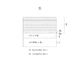
図1は、本発明の実施の形態1における半導体素子の製造方法によって製造された多重量子井戸構造を示す断面図である。多重量子井戸構造3は、Sをドープしたn型InP基板1の上に、InGaAsバッファ層2を介在させて形成されている。多重量子井戸構造3における量子井戸のペアは、厚み5nmのGaAsSb3aと、厚み5nmのInGaAs3bとからなる。いずれも、ノンドープである。GaAsSb3aが、InGaAsバッファ層に、直接、接して形成される。本実施の形態では、多重量子井戸構造3は、250ペアの量子井戸を備えている。本実施の形態では、250ペアの量子井戸からなる多重量子井戸構造3が、全有機MOVPE法で形成された点に特徴がある。
(Embodiment 1)
FIG. 1 is a cross-sectional view showing a multiple quantum well structure manufactured by the method for manufacturing a semiconductor device in the first embodiment of the present invention. The multiple
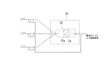
多重量子井戸構造3を形成した全有機MOVPE法の成膜装置70の配管系統等を、図2に示す。反応室(チャンバ)30内に石英管35が配置され、その石英管35に、原料ガスが導入される。石英管35中には、基板テーブル51が、回転自在に、かつ気密性を保つように配置される。基板テーブル51には、基板加熱用のヒータ51hが設けられる。成膜途中のウエハ10aの表面の温度は、反応室30の天井部に設けられたウィンドウ21を通して、赤外線温度モニタ装置20によりモニタされる。このモニタされる温度が、成長するときの温度、または成膜温度もしくは基板温度等と呼ばれる温度である。本発明における製造方法における、温度400℃以上かつ560℃以下で多重量子井戸構造を形成する、というときの400℃以上および560℃以下は、この温度モニタで計測される温度である。石英管35からの強制排気は真空ポンプによって行われる。
FIG. 2 shows a piping system of the all-organic MOVPE
原料ガスは、石英管35に連通する配管によって、供給される。全有機MOVPE法は、原料ガスをすべて有機金属気体の形態で供給する点に特徴がある。図2では、不純物等の原料ガスは明記していないが、不純物も有機金属気体の形態で導入される。有機金属気体の原料は、恒温槽に入れられて一定温度に保持される。搬送ガスには、水素(H2)および窒素(N2)が用いられる。有機金属気体は、搬送ガスによって搬送され、また真空ポンプで吸引されて石英管35に導入される。搬送ガスの量は、MFC(Mass Flow Controller:流量制御器)によって精度よく調節される。多数の、流量制御器、電磁弁等は、マイクロコンピュータによって自動制御される。
The source gas is supplied by a pipe communicating with the
図1に示すウエハ10の製造方法について説明する。まず、Sドープn型InP基板1に、n型InPバッファ層2を、厚み10nmに、エピタキシャル成長させる。n型のドーピングには、TeESi(テトラエチルシラン)を用いた。このときの原料ガスには、TMIn(トリメチルインジウム)およびTBP(ターシャリーブチルホスフィン)を用いる。このInPバッファ層2の成長には、無機原料のPH3(ホスフィン)を用いて行っても良い。このInPバッファ層2の成長では、成長温度を600℃程度あるいは600℃程度以下で行っても、下層に位置するInP基板の結晶性は600℃程度の加熱で劣化することはない。しかし、実施の形態2で説明するInP窓層を形成するときには、下層にGaAsSbを含む多重量子井戸構造が形成されているので、基板温度は、たとえば温度400℃以上かつ560℃以下の範囲に厳格に維持する必要がある。その理由として、600℃程度に加熱すると、GaAsSbが熱のダメージを受けて結晶性が大幅に劣化する点、および、400℃未満の温度としてInP窓層を形成すると、原料ガスの分解効率が大幅に低下するため、InP層内の不純物濃度が増大し高品質なInP窓層を得られない点があげられる。次いで、InPバッファ層2の上に、n型ドープしたInGaAs層を、厚み0.15μm(150nm)に成長する。このInGaAs層も図1中ではバッファ層2に含まれる。
A method for manufacturing the
次いで、InGaAs/GaAsSbを量子井戸のペアとするタイプIIの多重量子井戸構造3を形成する。量子井戸におけるGaAsSb3aは5nmの厚み、またInGaAs3bは厚み5nmとするのがよい。図1では、250ペアの量子井戸を積層して多重量子井戸構造3を形成している。GaAsSb3aの成膜では、トリエチルガリウム(TEGa)、ターシャリーブチルアルシン(TBAs)およびトリメチルアンチモン(TMSb)を用いる。また、InGaAs3bについては、TEGa、TMIn、およびTBAsを用いることができる。これらの原料ガスは、すべて有機金属気体であり、化合物の分子量は大きい。このため、400℃以上かつ560℃以下の比較的低温で完全に分解して、結晶成長に寄与することができる。多重量子井戸構造3を全有機MOVPEによって、量子井戸の界面の組成変化を急峻にするすることができる。
Next, a type II multiple
Ga(ガリウム)の原料としては、TEGa(トリエチルガリウム)でもよいし、TMGa(トリメチルガリウム)でもよいが、望ましくはTEGaがよい。これは、TEGaのほうが結晶中の不純物濃度を低減できるからである。特に量子井戸層内部の不純物となる炭素濃度は、TMGaを使用した場合は1×1016cm−3以上となるが、TEGaを使用した場合は1×1016cm−3未満とすることができる。In(インジウム)の原料としては、TMIn(トリメチルインジウム)でもよいし、TEIn(トリエチルインジウム)でもよいが、望ましくはTMInがよい。これは、TMInのほうがIn組成の制御性に優れているためである。As(砒素)の原料としては、TBAs(ターシャリーブチルアルシン)でもよいし、TMAs(トリメチル砒素)でもよいが、望ましくはTBAsがよい。これは、TBAsのほうが結晶中の不純物濃度を低減できるからである。特に量子井戸層内部の不純物となる炭素濃度は、TMAsを使用した場合は1×1016cm−3以上となるが、TBAsを使用した場合は1×1016cm−3未満とすることができる。Sb(アンチモン)の原料としては、TMSb(トリメチルアンチモン)でもよいし、TESb(トリエチルアンチモン)でもよい、また、TIPSb(トリイソプロピルアンチモン)、また、TDMASb(トリジメチルアミノアンチモン)でもよいが、望ましくはTESbがよい。これは、TESbのほうが結晶中の不純物濃度を低減できるからである。特に量子井戸層内部の不純物となる炭素濃度は、TMSbまたはTIPSbまたはTDMASbを使用した場合は1×1016cm−3以上となるが、TESbを使用した場合は1×1016cm−3未満とすることができる。これによって、多重量子井戸層の不純物濃度が小さく、その結晶性に優れた半導体素子を得ることができる。この結果、たとえば受光素子等に用いた場合、暗電流の小さい、かつ、感度が大きい受光素子を得ることができる。さらには、その受光素子を用いて、より鮮明な像を撮像するこが可能となる撮像装置を得ることができる。 As a raw material of Ga (gallium), TEGa (triethylgallium) or TMGa (trimethylgallium) may be used, but TEGa is preferable. This is because TEGa can reduce the impurity concentration in the crystal. In particular, the concentration of carbon that is an impurity inside the quantum well layer is 1 × 10 16 cm −3 or more when TMGa is used, but can be less than 1 × 10 16 cm −3 when TEGa is used. . As a raw material of In (indium), TMIn (trimethylindium) or TEIn (triethylindium) may be used, but TMIn is preferable. This is because TMIn is superior in controllability of In composition. As a raw material of As (arsenic), TBAs (tertiary butylarsine) or TMAs (trimethylarsenic) may be used, but TBAs is preferable. This is because TBAs can reduce the impurity concentration in the crystal. In particular, the carbon concentration that is an impurity inside the quantum well layer is 1 × 10 16 cm −3 or more when TMAs is used, but can be less than 1 × 10 16 cm −3 when TBAs is used. . The raw material of Sb (antimony) may be TMSb (trimethylantimony), TESb (triethylantimony), TIPSb (triisopropylantimony), or TDMASb (tridimethylaminoantimony). TESb is good. This is because TESb can reduce the impurity concentration in the crystal. In particular, the carbon concentration that becomes an impurity inside the quantum well layer is 1 × 10 16 cm −3 or more when TMSb, TIPSb, or TDMASb is used, but less than 1 × 10 16 cm −3 when TESb is used. can do. As a result, a semiconductor element having a low impurity concentration in the multiple quantum well layer and excellent crystallinity can be obtained. As a result, for example, when used in a light receiving element, a light receiving element with a small dark current and a high sensitivity can be obtained. Furthermore, an imaging apparatus that can capture a clearer image using the light receiving element can be obtained.
次に、全有機MOVPE法によって、多重量子井戸構造3を形成するときの原料ガスの流れ状態について説明する。図3は、原料ガスが、配管を搬送されて、石英管35に導入されて排気される、流れを示す平面図である。原料ガスは3種類のみの配管を示しているが、十数種類の原料ガスであっても、電磁バルブの開閉によって制御されるという基本構造は同じである。
原料ガスは、流量の制御は、図2に示す流量制御器(MFC)によって制御された上で、石英管35への流入を電磁バルブの開閉によってオンオフされる。そして、石英管35からは、真空ポンプによって強制的に排気される。図3に示すように、原料ガスの流れに停滞が生じる部分はなく、円滑に自動的に行われる。よって、量子井戸のペアを形成するときの組成の切り替えは、迅速に行われる。
図3に示すように、基板テーブル51は回転するので、原料ガスの温度分布は、原料ガスの流入側または出口側のような方向性をもたない。また、ウエハ10aは、基板テーブル51上を公転するので、ウエハ10aの表面近傍の原料ガスの流れは、乱流状態にあり、ウエハ10aの表面近傍の原料ガスであっても、ウエハ10aに接する原料ガスを除いて導入側から排気側への大きな流れ方向の速度成分を有する。したがって、基板テーブル51からウエハ10aを経て、原料ガスへと流れる熱は、大部分、常時、排気ガスと共に排熱される。このため、ウエハ10aから表面を経て原料ガス空間へと、垂直方向に大きな温度勾配または温度段差が発生する。
さらに、本発明の実施の形態では、基板温度を400℃以上かつ560℃以下という低温域に加熱される。このような低温域の基板表面温度でTBAsなどを原料とした全有機MOVPE法を用いる場合、その原料の分解効率が良いので、ウエハ10aにごく近い範囲を流れる原料ガスで多重量子井戸構造の成長に寄与する原料ガスは、成長に必要な形に効率よく分解したものに限られる。
Next, the flow state of the source gas when the multiple
The flow rate of the source gas is controlled by a flow rate controller (MFC) shown in FIG. 2, and the flow into the
As shown in FIG. 3, since the substrate table 51 rotates, the temperature distribution of the source gas does not have the directivity as on the inflow side or the outlet side of the source gas. Further, since the
Furthermore, in the embodiment of the present invention, the substrate temperature is heated to a low temperature range of 400 ° C. or more and 560 ° C. or less. When the all organic MOVPE method using TBAs or the like as a raw material at such a low temperature substrate surface temperature is used, the decomposition efficiency of the raw material is good, so that the growth of a multiple quantum well structure with a raw material gas flowing in a range very close to the
また図4(a)は有機金属分子の流れと温度の流れを示す図であり、図4(b)は基板表面における有機金属分子の模式図である。これらの図は、多重量子井戸構造のヘテロ界面で急峻な組成変化を得るために、表面温度の設定が重要であることを説明するための図である。
ウエハ10aの表面はモニタされる温度とされているが、ウエハ表面から少し原料ガス空間に入ると、上述のように、急激に温度低下または大きな温度段差が生じる。このため分解温度がT1℃の原料ガスの場合、基板表面温度は、(T1+α)に設定し、このαは、温度分布のばらつき等を考慮して決める。ウエハ10a表面から原料ガス空間にかけて急激で大きな温度降下または温度段差がある状況において、図4(b)に示すような、大サイズの有機金属分子がウエハ表面をかすめて流れるとき、分解して結晶成長に寄与する化合物分子は表面に接触する範囲、および表面から数個分の有機金属分子の厚み範囲、のものに限られると考えられる。したがって、図4(b)に示すように、ウエハ表面に接する範囲の有機金属分子、および、ウエハ表面から数個分の有機金属分子の厚み範囲以内に位置する分子、が、主として、結晶成長に寄与して、それより外側の有機金属分子は、ほとんど分解せずに石英管35の外に排出される、と考えられる。ウエハ10aの表面付近の有機金属分子が分解して結晶成長したとき、外側に位置する有機金属分子が補充に入る。
逆に考えると、ウエハ表面温度を有機金属分子が分解する温度よりほんのわずかに高くすることで、結晶成長に参加できる有機金属分子の範囲をウエハ10a表面上の薄い原料ガス層に限定することができる。
FIG. 4A is a diagram showing the flow of organometallic molecules and the flow of temperature, and FIG. 4B is a schematic diagram of organometallic molecules on the substrate surface. These diagrams are used to explain the importance of setting the surface temperature in order to obtain a steep composition change at the heterointerface of the multiple quantum well structure.
The surface of the
In other words, the range of the organometallic molecules that can participate in crystal growth is limited to a thin source gas layer on the surface of the
上記のことから、真空ポンプで強制排気しながら上記ペアの化学組成に適合した原料ガスを電磁バルブで切り替えて導入するとき、わずかの慣性をもって先の化学組成の結晶を成長させたあとは、先の原料ガスの影響を受けず、切り替えられた化学組成の結晶を成長させることができる。その結果、ヘテロ界面での組成変化を急峻にすることができる。これは、先の原料ガスが、石英管35内に実質的に残留しないことを意味しており、ウエハ10aにごく近い範囲を流れる原料ガスで多重量子井戸構造の成長に寄与する原料ガスは、成長に必要な形に効率よく分解したものに限られる(要因1)ことに起因する。すなわち、図3から分かるように、量子井戸の一方の層を形成させたあと、真空ポンプで強制排気しながら電磁バルブを開閉して、他方の層を形成する原料ガスを導入したとき、少しの慣性をもって結晶成長に参加する有機金属分子はいるが、その補充をする一方の層の分子はほとんど排気されて、なくなっている。ウエハ表面温度を、有機金属分子の分解温度に近づけるほど、結晶成長に参加する有機金属分子の範囲(ウエハ表面からの範囲)は小さくなる。
この多重量子井戸構造を形成する場合、600℃程度の温度範囲で成長すると多重量子井戸構造のGaAsSb層に相分離が起こり、清浄で平坦性に優れた多重量子井戸構造の結晶成長表面、および、優れた周期性と結晶性を有する多重量子井戸構造を得ることができない。このことから、成長温度を400℃以上かつ560℃以下という温度範囲にする(要因2)が、この成膜法を全有機MOVPE法にして、原料ガスすべてを分解効率の良い有機金属気体にすること(要因3)に、要因1が強く依拠している。
From the above, when the source gas suitable for the chemical composition of the pair is switched by the electromagnetic valve and forcedly evacuated by the vacuum pump, after the crystal of the previous chemical composition is grown with slight inertia, Thus, it is possible to grow a crystal having a switched chemical composition without being affected by the source gas. As a result, the composition change at the hetero interface can be made steep. This means that the previous source gas does not substantially remain in the
When forming this multi-quantum well structure, phase growth occurs in the GaAsSb layer of the multi-quantum well structure when grown in a temperature range of about 600 ° C., and the crystal growth surface of the multi-quantum well structure that is clean and excellent in flatness, and A multiple quantum well structure having excellent periodicity and crystallinity cannot be obtained. For this reason, the growth temperature is set to a temperature range of 400 ° C. or more and 560 ° C. or less (Factor 2). This film-forming method is changed to an all-organic MOVPE method, and all the source gases are converted into organometallic gases with high decomposition efficiency.
(実施の形態2)
図5は、本発明の実施の形態2における半導体素子を示す断面図である。この半導体素子10は、フォトダイオードの受光素子である。n型InP基板1/バッファ層2/タイプIIの多重量子井戸構造3(InGaAs3a/GaAsSb3b)、の段階までは、実施の形態1の図1の構造と同じである。タイプIIの多重量子井戸構造3の上には、あとで詳しく説明する拡散濃度分布を調整する作用を担うInGaAs層4が位置し、そのInGaAs層4の上にInP窓層5が位置している。InP窓層5の表面から、所定領域にp型不純物のZnが導入されてp型領域15が設けられ、その先端部にpn接合またはpi接合が形成される。このpn接合またはpi接合に、逆バイアス電圧を印加して空乏層を形成して、光電子変換による電荷を捕捉して、電荷量に画素の明るさを対応させる。p型領域15またはpn接合もしくはpi接合は、画素を構成する主要部である。p型領域15にオーミック接触するp側電極11は画素電極であり、共通の接地電位にされるn側電極(図示せず)との間で、上記の電荷を画素ごとに読み出す。p型領域15の周囲の、InP窓層表面は絶縁保護膜9によって被覆される。
多重量子井戸構造を形成したあと、InP窓層5の形成まで、全有機MOVPE法によって同じ成膜室または石英管35の中で成長を続けることが、一つのポイントになる。すなわち、InP窓層5の形成の前に、成膜室からウエハ10aを取り出して、別の成膜法によってInP窓層5を形成することがないために、再成長界面を持たない点が一つのポイントである。すなわち、InGaAs層4とInP窓層5とは、石英管35内において連続して形成されるので、界面17は再成長界面ではない。このため、酸素および炭素の濃度がいずれも所定レベル以下であり、p型領域15と界面17との交差線において電荷リークが生じることはない。
(Embodiment 2)
FIG. 5 is a sectional view showing a semiconductor element according to the second embodiment of the present invention. This
One point is to continue the growth in the same film formation chamber or
本実施の形態では、図5に示すように、多重量子井戸構造3の上に、厚み1.0μmのノンドープInGaAs層4を形成する。このInGaAs層4は、InP窓層5を形成したあと、選択拡散法によってInP窓層5からp型不純物のZnを多重量子井戸構造3に届くように導入するとき、高濃度のZnが多重量子井戸構造3に進入すると、結晶性を害するので、その調整のために設ける。このため、このInGaAs層4を拡散濃度分布調整層と呼ぶ場合がある。InGaAs層4内において、Zn濃度は、InP窓層の側では、1×1018cm−3〜3×1019cm−3程度の高濃度であっても、多重量子井戸構造3の側では5×1016cm−3以下と、急減する濃度分布とするのがよい。InGaAs層4を挿入することによって、Znの拡散濃度分布を上記のような形態にすることが可能となる。上記の選択拡散によってp型不純物領域15が形成され、その先端部にpn接合またはpi接合が形成される。InGaAsによって拡散濃度分布調整層を形成することで、不純物濃度(Zn濃度)が低くても、受光素子の電気抵抗を低くすることができる。電気抵抗を低くすることで、応答性を高めて良好な画質の動画を得ることができる。
InGaAs拡散濃度分布調整層4の上に、同じ石英管35内にウエハ10aを配置したまま連続して、アンドープのInP窓層を、全有機MOVPE法によって厚み0.8μmにエピタキシャル成長する。原料ガスには、上述のように、トリメチルインジウム(TMIn)およびターシャリーブチルホスフィン(TBP)を用いる。この原料ガスの使用によって、InP窓層5の成長温度を400℃以上かつ560℃以下に、さらには535℃以下にすることができる。この結果、InP窓層5の下に位置する多重量子井戸構造のGaAsSb3aが熱のダメージを受けることがなく、多重量子井戸の結晶性が害されることがない。InP窓層を形成するときには、下層にGaAsSbを含む多重量子井戸構造が形成されているので、基板温度は、たとえば温度400℃以上かつ560℃以下の範囲に厳格に維持する必要がある。その理由として、600℃程度に加熱すると、GaAsSbが熱のダメージを受けて結晶性が大幅に劣化する点、および、400℃未満の温度としてInP窓層を形成すると、原料ガスの分解効率が大幅に低下するため、InP層内の不純物濃度が増大し高品質なInP窓層を得られない点があげられる。
In the present embodiment, as shown in FIG. 5, a non-doped
On the InGaAs diffusion concentration
上記したように、従来は、多重量子井戸構造をMBE法によって形成する必要があった。ところが、MBE法によってInP窓層5を成長するには、燐原料に固体の原料を用いる必要があり、安全性などの点で問題があった。また製造能率という点でも改良の余地があった。図6は、多重量子井戸構造103およびInGaAs層104をMBE法によって形成し、その後、大気中に出して、MOVPE法によってInP窓層105を形成した受光素子110を示す図である。この受光素子110の構造は、大部分は、図5の受光素子10と組成的に同じである。すなわち、InP基板101/多重量子井戸構造103/InGaAs拡散濃度分布調整層104/InP窓層105、のエピタキシャル層で形成されている。画素の主要部をなすp型領域115、画素電極を構成するp側電極111、絶縁保護膜109、なども図5の受光素子と同じである。
異なる点は、InGaAs層104とInP窓層105との界面117である。この界面117は、いったん大気に露出された再成長界面であり、二次イオン質量分析によって、酸素濃度が1×1017cm−3以上、および炭素濃度が1×1017cm−3以上のうち、少なくとも一つを満たすことによって特定することができる。再成長界面117は、p型領域115と交差線117aを形成し、交差線117aで電荷リークを生じて、画質を著しく劣化させる。
また、たとえばInP窓層105を単なるMOVPE法によると、燐の原料にホスフィン(PH3)を用いるため、分解温度が高く、下層に位置するGaAsSbの熱によるダメージの発生を誘起して多重量子井戸構造の結晶性を害することとなる。
As described above, conventionally, it has been necessary to form a multiple quantum well structure by the MBE method. However, in order to grow the InP window layer 5 by the MBE method, it is necessary to use a solid raw material as the phosphorus raw material, which is problematic in terms of safety. There was also room for improvement in terms of manufacturing efficiency. FIG. 6 is a diagram showing a
The difference is an
In addition, for example, when the
図7は、図5の受光素子10の製造方法のフローチャートである。この製造方法によれば、原料ガスに有機金属気体のみを用いて(要因3)成長温度を低下させること(要因2)、および、InP窓層5の形成が終了するまで、一貫して同じ成膜室または石英管35の中で形成するので、再成長界面を持たないこと(要因4)が重要である。これによって、電荷リークが少ない、結晶性に優れた、2μm〜5μmの波長領域に受光感度を持つフォトダイオードを能率良く、大量に製造することができる。
FIG. 7 is a flowchart of a method for manufacturing the
本実施の形態では、多重量子井戸構造をタイプIIとする。タイプIの量子井戸構造では、バンドギャップエネルギの小さい半導体層を、バンドギャップエネルギの大きい半導体層で挟みながら、近赤外域に受光感度を持たせる場合、小さいバンドギャップエネルギの半導体層のバンドギャップにより受光感度の波長上限(カットオフ波長)が定まる。すなわち、光による電子または正孔の遷移は、小さいバンドギャップエネルギの半導体層内で行われる(直接遷移)。この構造の場合、カットオフ波長をより長波長域まで拡大する材料は、III−V族化合物半導体内で、非常に限定される。これに対して、タイプIIの量子井戸構造では、フェルミエネルギを共通にして異なる2種の半導体層が交互に積層されたとき、第1の半導体の伝導帯と、第2の半導体の価電子帯とのエネルギ差が、受光感度の波長上限(カットオフ波長)を決める。すなわち、光による電子または正孔の遷移は、第2の半導体の価電子帯と、第1の半導体の伝導帯との間で行われる(間接遷移)。このため、第2の半導体の価電子帯のエネルギを、第1の半導体の価電子帯より高くし、かつ第1の半導体の伝導帯のエネルギを、第2の半導体の伝導帯のエネルギより低くすることにより、1つの半導体内の直接遷移による場合よりも、受光感度の長波長化を実現しやすい。 In the present embodiment, the multiple quantum well structure is type II. In the type I quantum well structure, when a semiconductor layer having a small band gap energy is sandwiched between semiconductor layers having a large band gap energy and light receiving sensitivity is provided in the near infrared region, the band gap of the semiconductor layer having a small band gap energy The upper limit wavelength (cutoff wavelength) of the light receiving sensitivity is determined. That is, transition of electrons or holes due to light is performed in a semiconductor layer having a small band gap energy (direct transition). In the case of this structure, the material for extending the cut-off wavelength to a longer wavelength region is very limited within the III-V compound semiconductor. On the other hand, in the type II quantum well structure, when two different semiconductor layers having the same Fermi energy are alternately stacked, the conduction band of the first semiconductor and the valence band of the second semiconductor are obtained. The upper limit of the wavelength (cutoff wavelength) of the light receiving sensitivity is determined. That is, transition of electrons or holes by light is performed between the valence band of the second semiconductor and the conduction band of the first semiconductor (indirect transition). For this reason, the energy of the valence band of the second semiconductor is made higher than that of the first semiconductor, and the energy of the conduction band of the first semiconductor is made lower than the energy of the conduction band of the second semiconductor. By doing so, it is easier to realize a longer wavelength of light receiving sensitivity than in the case of direct transition in one semiconductor.
(実施例1)
図5に示す受光素子(本発明例)を、実施の形態1および2による方法で製造して、予備的な評価を行った。評価項目および評価結果はつぎのとおりである。また、比較例は、図6に示した受光素子であり、多重量子井戸構造の形成にMBE法を用い、InP窓層の形成では、MOVPE法を用いてV族原料に、アルシン(AsH3)およびホスフィン(PH3)を用いた。InP窓層の成長温度は、本発明例では535℃としたのに対して、比較例では600℃とした。
1.InP窓層の表面状態
本発明例では、清浄で平坦性に優れた表面を得ることができた。これに対して、比較例では、InP窓層は強度の表面あれを生じていた。
2.多重量子井戸構造のX線回折
X線回折法によってタイプIIの多重量子井戸構造の周期性の評価を行った。評価はX線回折パターンの所定ピークにおける半値幅により行った。本発明例では、多重量子井戸構造のX線回折パターンピーク値の半値幅は、80秒であった。これに対して、比較例では、X線回折パターンのピークの半値幅は、150秒であった。これより、本発明例において、多重量子井戸構造の周期性および結晶性が、格段に優れていることが判明した。
3.PL発光強度
本発明例では、波長2.4μmの領域に良好なPL発光強度を得ることができた。これに対して、比較例では、評価可能なPL発光を得ることができなかった。
Example 1
The light receiving element (example of the present invention) shown in FIG. 5 was manufactured by the method according to
1. Surface state of InP window layer In the example of the present invention, it was possible to obtain a clean and excellent surface. On the other hand, in the comparative example, the InP window layer had a strong surface roughness.
2. X-ray diffraction of a multiple quantum well structure The periodicity of a type II multiple quantum well structure was evaluated by an X-ray diffraction method. The evaluation was performed based on the half width at a predetermined peak of the X-ray diffraction pattern. In the example of the present invention, the half width of the peak value of the X-ray diffraction pattern of the multiple quantum well structure was 80 seconds. On the other hand, in the comparative example, the half width of the peak of the X-ray diffraction pattern was 150 seconds. From this, it was found that the periodicity and crystallinity of the multi-quantum well structure were remarkably excellent in the inventive examples.
3. PL emission intensity In the example of the present invention, a good PL emission intensity could be obtained in a wavelength region of 2.4 μm. On the other hand, in the comparative example, it was not possible to obtain an evaluable PL light emission.
(実施例2)
図5に示す受光素子を、本発明による製造方法で製造した試験体である本発明例A1、A3〜A6、および本発明とは異なる製造方法で製造した試験体、比較例B1〜B3、参考例A2、A7について、結晶性の評価、受光素子の暗電流の評価を行った。暗電流は、Vr=−5ボルトでの100μm径での値である。
(本発明例A1):全有機MOVPEによる、タイプIIMQW受光層(温度510℃)およびInP窓層の成長(温度510℃)
(参考例A2):全有機MOVPEによる、タイプIIMQW受光層(温度380℃)およびInP窓層の成長(温度510℃)
(本発明例A3):全有機MOVPEによる、タイプIIMQW受光層(温度400℃)およびInP窓層の成長(温度510℃)
(本発明例A4):全有機MOVPEによる、タイプIIMQW受光層(温度450℃)およびInP窓層の成長(温度510℃)
(本発明例A5):全有機MOVPEによる、タイプIIMQW受光層(温度535℃)およびInP窓層の成長(温度510℃)
(本発明例A6):全有機MOVPEによる、タイプIIMQW受光層(温度560℃)およびInP窓層の成長(温度510℃)
(参考例A7):全有機MOVPEによる、タイプIIMQW受光層(温度580℃)およびInP窓層の成長(温度510℃)
本発明例A1、A3〜A6では、全有機MOVPEで、タイプII型(InGaAs/GaAsSb)MQWを成長するとき、温度400℃〜560℃の範囲に変えている。参考例A2は380℃、A7は580℃で成長している。その他の条件は同じである。
(比較例B1:非特許文献1による方法):MBEによるタイプIIMQW受光層の成長(温度400℃)、および通常のMOVPEによるInP窓層の成長(温度600℃)
(比較例B2:非特許文献2による方法):通常のMOVPEによるタイプIIMQW受光層の成長(温度510℃)、および全有機MOVPEによるInP窓層の成長(温度510℃)
(比較例B3):通常のMOVPEによるタイプIIMQW受光層の成長(温度600℃)、および全有機MOVPEによるInP窓層の成長(温度510℃)
比較例では、タイプII型(InGaAs/GaAsSb)MQWを、MBE法(比較例B1)、通常のMOVPE法(比較例B1,B2)によって成長している。
上記の試験帯体の製造条件およびその評価の結果を、表1および表2に示す。
(Example 2)
The light-receiving element shown in FIG. 5 is a test body manufactured by a manufacturing method according to the present invention, A1 and A3 to A6 of the present invention, and a test body manufactured by a manufacturing method different from the present invention, comparative examples B1 to B3, reference For Examples A2 and A7, the crystallinity was evaluated and the dark current of the light receiving element was evaluated. The dark current is a value at a diameter of 100 μm at Vr = −5 volts.
(Invention Sample A1): Growth of type II MQW light-receiving layer (temperature: 510 ° C.) and InP window layer (temperature: 510 ° C.) by all organic MOVPE
Reference Example A2: Type II MQW light-receiving layer (temperature 380 ° C.) and InP window layer growth (temperature 510 ° C.) by all organic MOVPE
(Invention Sample A3): Growth of type II MQW light-receiving layer (
(Invention Sample A4): Growth of type II MQW light-receiving layer (temperature 450 ° C.) and InP window layer (temperature 510 ° C.) by all organic MOVPE
(Invention Sample A5): Growth of type II MQW light-receiving layer (temperature 535 ° C.) and InP window layer (temperature 510 ° C.) by all organic MOVPE
(Invention Sample A6): Growth of type II MQW light-receiving layer (temperature 560 ° C.) and InP window layer (temperature 510 ° C.) by all organic MOVPE
(Reference Example A7): Growth of type II MQW light-receiving layer (temperature 580 ° C.) and InP window layer (temperature 510 ° C.) by all organic MOVPE
In Invention Examples A1, A3 to A6, when growing type II (InGaAs / GaAsSb) MQW with all organic MOVPE, the temperature is changed to a range of 400 ° C. to 560 ° C. Reference Example A2 grows at 380 ° C. and A7 grows at 580 ° C. Other conditions are the same.
(Comparative Example B1: Method according to Non-Patent Document 1): Growth of type II MQW light-receiving layer by MBE (
(Comparative Example B2: Method according to Non-Patent Document 2): Growth of type II MQW light-receiving layer by normal MOVPE (temperature 510 ° C.) and growth of InP window layer by total organic MOVPE (temperature 510 ° C.)
(Comparative Example B3): Growth of type II MQW light-receiving layer by normal MOVPE (
In the comparative example, type II (InGaAs / GaAsSb) MQW is grown by the MBE method (Comparative Example B1) and the normal MOVPE method (Comparative Examples B1 and B2).
Tables 1 and 2 show the manufacturing conditions of the test strip and the results of the evaluation.
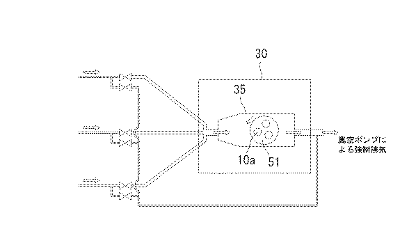
表1によれば、比較例B1〜B3では、MQWのX線回折ピークの半値幅は、150秒(比較例B1)、150秒(比較例B2)、および170秒(比較例B3)と、広くなり、結晶性が良好でない結果が得られた。また、比較例B1〜B3について、波長2.4μmのPL発光は生じなかった。さらに、InP窓層の表面性状については、比較例B1〜B3、参考例A2およびA7について、強度の表面荒れが生じていた。フォトダイオードでの暗電流は、比較例B1で5μA、比較例B2で4μAであった。また参考例A2で5μA、参考例A7で8μAであった。InP窓層の表面性状については、サイズ10μm程度以上の欠陥や荒れが多数確認された場合、「表面荒れ発生」と判定し、上記サイズの欠陥や荒れがほとんど確認されない場合を、「清浄で平坦性に優れた表面」と判定した。
これに対して、表1および表2に示すように、全有機MOVPE法でMQWを成長しても、MQWの成長温度が380℃(参考例A2)のように極端に低い場合、および580℃(参考例A7)のように極端に高い場合に、X線回折ピークの半値幅が、125秒および150秒と、大きな値となった。PL発光は、この参考例A2、A7では生じなかった。本発明例A1、A3〜A6では、X線回折ピークの半値幅は、80秒、55秒〜95秒と狭い値が得られ、結晶性は良好であり、PL発光も生じた。また、InP窓層の表面性状については、参考例A2、A7以外は清浄で平坦性に優れた表面となった。さらに暗電流についても、参考例A2,A7以外は、0.4μA(本発明例A1)、0.9μA(本発明例A3)、0.7μA(本発明例A4)、0.4μA(本発明例A5)、0.8μA(本発明例A6)と、低い良好な暗電流特性が得られた。
本実施例の結果によれば、本発明の製造方法により、温度400℃〜560℃でタイプII型(InGaAs/GaAsSb)MQWを全有機MOVPEで成長することにより、良好な結晶性を得ることができ、かつInP窓層の表面も平坦性に優れ、その結果、暗電流を低く抑えることができた。本発明の最も広い範囲に属する製造方法(全有機MOVPE法による結晶成長)による場合であっても、温度400℃〜560℃を外れる温度で成長した場合、良好な結果を得ることができなかった。また、比較例B1〜B3のように、タイプII型(InGaAs/GaAsSb)MQWを全有機MOVPE法によらずに成長させた場合、結晶性の劣化、それに起因するInP窓層の表面性状の劣化を確認した。
According to Table 1, in Comparative Examples B1 to B3, the half width of the MQW X-ray diffraction peak is 150 seconds (Comparative Example B1), 150 seconds (Comparative Example B2), and 170 seconds (Comparative Example B3). The result was wide and the crystallinity was not good. Moreover, about Comparative Examples B1-B3, PL light emission with a wavelength of 2.4 micrometers did not arise. Further, regarding the surface properties of the InP window layer, the surface roughness of the strength occurred in Comparative Examples B1 to B3 and Reference Examples A2 and A7. The dark current in the photodiode was 5 μA in Comparative Example B1 and 4 μA in Comparative Example B2. In Reference Example A2, it was 5 μA, and in Reference Example A7, it was 8 μA. As for the surface properties of the InP window layer, when many defects or roughness of about 10 μm or more are confirmed, it is determined that “surface roughness has occurred”, and when the defects and roughness of the above size are hardly confirmed, “clean and flat It was determined that the surface had excellent properties.
On the other hand, as shown in Table 1 and Table 2, even when MQW is grown by the all organic MOVPE method, the growth temperature of MQW is extremely low as 380 ° C. (Reference Example A2), and 580 ° C. When it was extremely high as in (Reference Example A7), the full width at half maximum of the X-ray diffraction peak was 125 seconds and 150 seconds. PL light emission did not occur in Reference Examples A2 and A7. In Invention Examples A1, A3 to A6, the half width of the X-ray diffraction peak was as narrow as 80 seconds and 55 seconds to 95 seconds, the crystallinity was good, and PL light emission was also generated. As for the surface properties of the InP window layer, surfaces other than Reference Examples A2 and A7 were clean and had excellent flatness. Further, with respect to dark current, except for Reference Examples A2 and A7, 0.4 μA (Invention Example A1), 0.9 μA (Invention Example A3), 0.7 μA (Invention Example A4), 0.4 μA (Invention) Example A5), 0.8 μA (Invention Example A6), and low dark current characteristics were obtained.
According to the results of the present example, by the method of the present invention, it is possible to obtain good crystallinity by growing type II (InGaAs / GaAsSb) MQW with all organic MOVPE at a temperature of 400 ° C. to 560 ° C. In addition, the surface of the InP window layer was excellent in flatness, and as a result, dark current could be kept low. Even in the case of the production method (crystal growth by the all organic MOVPE method) belonging to the widest range of the present invention, good results could not be obtained when grown at a temperature outside the temperature range of 400 ° C to 560 ° C. . Moreover, when the type II type (InGaAs / GaAsSb) MQW is grown without using the all organic MOVPE method as in Comparative Examples B1 to B3, the crystallinity deteriorates and the surface properties of the InP window layer deteriorate due to the deterioration. It was confirmed.
(実施例3)
実施例2の本発明例A1において、量子井戸のペア数を50から1000の範囲で変化させた。すなわち図5に示す受光素子の構造において量子井戸のペア数を変えた。その他の成長条件は同一である。
(本発明例A1−1):全有機MOVPEによる、タイプIIMQW受光層(ペア数:50ペア)
(本発明例A1−2):全有機MOVPEによる、タイプIIMQW受光層(ペア数:150ペア)
(本発明例A1−3):全有機MOVPEによる、タイプIIMQW受光層(ペア数:250ペア)
(本発明例A1−4):全有機MOVPEによる、タイプIIMQW受光層(ペア数:350ペア)
(本発明例A1−5):全有機MOVPEによる、タイプIIMQW受光層(ペア数:450ペア)
(本発明例A1−6):全有機MOVPEによる、タイプIIMQW受光層(ペア数:700ペア)
(本発明例A1−7):全有機MOVPEによる、タイプIIMQW受光層(ペア数:850ペア)
(本発明例A1−8):全有機MOVPEによる、タイプIIMQW受光層(ペア数:1000ペア)
本発明例A1−1〜A1−8について、受光素子の暗電流および感度の評価を行った。暗電流は、Vr=5ボルトでの100μm径での値である。感度は逆バイアス電圧Vr=5ボルトでの1mm径で、波長2000nmの光に対する値である。評価結果を表3に示す。
(Example 3)
In Invention Example A1 of Example 2, the number of quantum well pairs was changed in the range of 50 to 1000. That is, the number of pairs of quantum wells was changed in the structure of the light receiving element shown in FIG. Other growth conditions are the same.
(Invention Sample A1-1): Type II MQW light-receiving layer made of all organic MOVPE (number of pairs: 50 pairs)
(Invention Sample A1-2): Type II MQW light-receiving layer made of all organic MOVPE (number of pairs: 150 pairs)
(Invention Sample A1-3): Type II MQW light-receiving layer made of all organic MOVPE (number of pairs: 250 pairs)
(Invention Sample A1-4): Type II MQW light-receiving layer made of all organic MOVPE (number of pairs: 350 pairs)
(Invention Sample A1-5): Type II MQW light-receiving layer made of all organic MOVPE (number of pairs: 450 pairs)
(Invention Sample A1-6): Type II MQW light-receiving layer made of all organic MOVPE (number of pairs: 700 pairs)
(Invention Sample A1-7): Type II MQW light-receiving layer made of all organic MOVPE (number of pairs: 850 pairs)
(Invention Sample A1-8): Type II MQW light-receiving layer made of all organic MOVPE (number of pairs: 1000 pairs)
For Inventive Examples A1-1 to A1-8, the dark current and sensitivity of the light receiving element were evaluated. The dark current is a value at a diameter of 100 μm at Vr = 5 volts. The sensitivity is a value with respect to light having a diameter of 1 mm at a reverse bias voltage Vr = 5 volts and a wavelength of 2000 nm. The evaluation results are shown in Table 3.
本発明例A1−1〜A1−6ではInP窓層は清浄で平坦性に優れた表面となった。受光素子の暗電流は、300nA〜600nAと、低い良好な暗電流特性が得られた。本発明例A1−7とA1−8では、InP窓層に表面荒れが発生した。受光素子の暗電流は、2μA(本発明例A1−7)、5μA(本発明例A1−8)と高く、暗電流不良となった。
一方、感度は、本発明例A1−1〜A1−6ではペア数を50から700に増加させるに従って、0.1A/Wから0.75A/Wまで増大した。本発明例A1−7とA1−8では、感度はそれぞれ0.7A/W、0.6A/Wとなった。
受光感度および暗電流と、量子井戸のペア数との関係を図8に示す。ペア数850以上では受光感度は高いが、暗電流は大きくなる。受光感度と暗電流とを共に実用レベル範囲にするペア数の範囲が存在する。
このあと実施例4において詳しいデータを説明するが、本発明例A1−1〜A1−8の受光素子に対応する構造の受光素子アレイを製造して、撮像装置を作製したところ、A1−3〜A1−6に対応する受光素子アレイを用いた場合のみ、冷却機構を用いて撮像装置の環境温度を0℃以下とすることでより鮮明な画像の撮像に成功した。一方で、A1−1、およびA1−2、およびA1−7、およびA1−8の受光素子を用いた場合は、冷却機構を用いて撮像装置の環境温度を0℃以下としても鮮明な画像を撮像することができなかった。
In Inventive Examples A1-1 to A1-6, the InP window layer had a clean and excellent surface. The dark current of the light receiving element was as low as 300 nA to 600 nA, and good dark current characteristics were obtained. In Invention Examples A1-7 and A1-8, surface roughness occurred in the InP window layer. The dark current of the light-receiving element was as high as 2 μA (Invention Sample A1-7) and 5 μA (Invention Sample A1-8), resulting in dark current failure.
On the other hand, in Examples A1-1 to A1-6 of the present invention, the sensitivity increased from 0.1 A / W to 0.75 A / W as the number of pairs was increased from 50 to 700. In inventive examples A1-7 and A1-8, the sensitivities were 0.7 A / W and 0.6 A / W, respectively.
FIG. 8 shows the relationship between the photosensitivity and dark current and the number of quantum well pairs. When the number of pairs is 850 or more, the light receiving sensitivity is high, but the dark current increases. There is a range of the number of pairs in which both the light receiving sensitivity and the dark current are in a practical level range.
Detailed data will be described later in Example 4. When a light receiving element array having a structure corresponding to the light receiving elements of Examples A1-1 to A1-8 of the present invention was manufactured and an imaging device was manufactured, A1-3 Only when the light receiving element array corresponding to A1-6 was used, a clearer image was successfully captured by setting the environmental temperature of the imaging apparatus to 0 ° C. or lower using the cooling mechanism. On the other hand, when the light receiving elements A1-1, A1-2, A1-7, and A1-8 are used, a clear image can be obtained even when the environmental temperature of the imaging apparatus is set to 0 ° C. or lower using the cooling mechanism. I couldn't take an image.
(実施例4)
実施例3の本発明例A1−3、およびA1−4、およびA1−5、において、InGaAs/GaAsSbを量子井戸のペアとするタイプIIの多重量子井戸構造3を形成する際に用いる原料を変化させた。すなわち図5に示す受光素子の構造において量子井戸の作製に用いる原料を変えた。作製した受光素子の構造は同一である。
(本発明例A1−3−1):全有機MOVPEによる、タイプIIMQW受光層(ペア数は250ペア、原料にTEGa、TMIn、TBAs,TMSbを用いる)
(本発明例A1−3−2):全有機MOVPEによる、タイプIIMQW受光層(ペア数は250ペア、原料にTEGa、TMIn、TBAs,TESbを用いる)
(本発明例A1−3−3):全有機MOVPEによる、タイプIIMQW受光層(ペア数は250ペア、原料にTEGa、TMIn、TMAs,TESbを用いる)
(本発明例A1−3−4):全有機MOVPEによる、タイプIIMQW受光層(ペア数は250ペア、原料にTEGa、TEIn、TBAs,TESbを用いる)
(本発明例A1−3−5):全有機MOVPEによる、タイプIIMQW受光層(ペア数は250ペア、原料にTMGa、TMIn、TBAs,TESbを用いる)
(本発明例A1−4−1):全有機MOVPEによる、タイプIIMQW受光層(ペア数は350ペア、原料にTEGa、TMIn、TBAs,TMSbを用いる)
(本発明例A1−4−2):全有機MOVPEによる、タイプIIMQW受光層(ペア数は350ペア、原料にTEGa、TMIn、TBAs,TESbを用いる)
(本発明例A1−5−1):全有機MOVPEによる、タイプIIMQW受光層(ペア数は450ペア、原料にTEGa、TMIn、TBAs,TMSbを用いる)
(本発明例A1−5−2):全有機MOVPEによる、タイプIIMQW受光層(ペア数は450ペア、原料にTEGa、TMIn、TBAs,TESbを用いる)
本発明例A1−3−1、およびA1−3−2、およびA1−3−3、およびA1−3−4、およびA1−3−5、およびA1−4−1、およびA1−4−2、およびA1−5−1、およびA1−5−2、について、同じ条件で受光素子アレイを製造して、撮像装置を作製して当該撮像装置での撮像の状況の評価を行った。受光素子アレイは、受光素子(画素)を320×256に配置して、全体で約8万画素の撮像装置とした。暗電流は、Vr=5ボルトでの100μm径での値である。評価結果を表4に示す。
Example 4
In the present invention examples A1-3, A1-4, and A1-5 of Example 3, the raw materials used when forming the type II multiple
(Invention Sample A1-3-1): Type II MQW light-receiving layer made of all organic MOVPE (the number of pairs is 250 pairs, and TEGa, TMIn, TBAs, and TMSb are used as raw materials)
(Invention Sample A1-3-2): Type II MQW light-receiving layer made of all organic MOVPE (number of pairs is 250 pairs, TEGa, TMIn, TBAs, and TESb are used as raw materials)
(Invention Sample A1-3-3): Type II MQW light-receiving layer made of all organic MOVPE (the number of pairs is 250 pairs, and TEGa, TMIn, TMAs, and TESb are used as raw materials)
(Invention Sample A1-3-4): Type II MQW light-receiving layer made of all organic MOVPE (the number of pairs is 250 pairs, and TEGa, TEIn, TBAs, and TESb are used as raw materials)
(Invention Sample A1-3-5): Type II MQW light-receiving layer made of all organic MOVPE (250 pairs, TMGa, TMIn, TBAs, TESb used as raw material)
(Invention Sample A1-4-1): Type II MQW light-receiving layer (350 pairs, TEGa, TMIn, TBAs, TMSb is used as a raw material) by all organic MOVPE
(Invention Sample A1-4-2): Type II MQW light-receiving layer (350 pairs, TEGa, TMIn, TBAs, and TESb are used as raw materials) by all organic MOVPE
(Invention Sample A1-5-1): Type II MQW light-receiving layer made of all organic MOVPE (450 pairs, TEGa, TMIn, TBAs, TMSb used as raw material)
(Invention Sample A1-5-2): Type II MQW light-receiving layer made of all organic MOVPE (450 pairs, TEGa, TMIn, TBAs, TESb used as raw material)
Invention Examples A1-3-1, A1-3-3, A1-3-3, A1-3-4, A1-3-5, A1-4-1, and A1-4-2 , And A1-5-1 and A1-5-2, the light receiving element array was manufactured under the same conditions, the imaging device was manufactured, and the imaging state of the imaging device was evaluated. In the light receiving element array, light receiving elements (pixels) are arranged in a size of 320 × 256, and the imaging device has a total of about 80,000 pixels. The dark current is a value at a diameter of 100 μm at Vr = 5 volts. The evaluation results are shown in Table 4.
本発明例でAs原料にTMAsを用いた試験体であるA1−3−3、および本発明例でIn原料にTEInを用いた試験体であるA1−3−4、および本発明例でGa原料にTMGaを用いた試験体であるA1−3−5では、作製した受光素子の受光径100μmでの暗電流は、3μA〜5μAとなり、実施例A1−3−2と比較して、暗電流が増加し、特性が悪化した。一方、本発明例でAs原料にTMAsを用いた試験体であるA1−3−3、および本発明例でIn原料にTEInを用いた試験体であるA1−3−4、および本発明例でGa原料にTMGaを用いた試験体であるA1−3−5では、感度は、0.1A/W〜0.3A/Wとなり、試験体A1−3−2と比較して、感度が低減し、特性が悪化した。
本発明例でSb原料にTESbを用いた試験体であるA1−3−2、およびA1−4−2、およびA1−5−2では、作製した受光素子の受光径100μmでの暗電流は、40nA〜50nAとなり、本発明例でSb原料にTMSbを用いた試験体であるA1−3−1、およびA1−4−1、およびA1−5−1とそれぞれ比較して、暗電流を低減することができ、極めて良好な暗電流特性が得られた。一方、本発明でSb原料にTESbを用いた試験体であるA1−3−2、およびA1−4−2、およびA1−5−2では、感度は、0.75A/W〜0.9A/Wとなり、本発明でSb原料にTMSbを用いた試験体であるA1−3−1、およびA1−4−1、およびA1−5−1とそれぞれ比較して、感度を増加させることができた。
本発明例A1−3−1、およびA1−3−2、およびA1−3−3、およびA1−3−4、およびA1−3−5、およびA1−4−1、およびA1−4−2、およびA1−5−1、およびA1−5−2、において作製した受光素子アレイを用いて撮像装置を作製したところ、受光素子の暗電流密度が0.5mA/cm2以下となる試験体である、A1−3−1、およびA1−4−2に対応する受光素子アレイを用いた場合のみ、冷却機構を用いずに、鮮明な画像の撮像に成功した。すなわち、受光素子の暗電流密度が0.5mA/cm2以下となる本発明例であるA1−3−1、およびA1−4−2の受光素子アレイを用いた場合のみ、撮像装置の環境温度が例えば0℃以上40℃以下となるような、より実用的な温度範囲でも、鮮明な画像を撮像することに成功した。
A1-3-3 which is a test body using TMAs as an As raw material in the inventive example, A1-3-4 which is a test body using TEIn as an In raw material in the inventive example, and a Ga raw material in the inventive example In A1-3-5, which is a test body using TMGa, the dark current at a light receiving diameter of 100 μm of the manufactured light receiving element is 3 μA to 5 μA, which is lower than that of Example A1-3-2. Increased and the characteristics deteriorated. On the other hand, in the present invention example, A1-3-3 which is a test body using TMAs as an As raw material, and in the present invention example, A1-3-4 which is a test body using TEIn as an In raw material, and the present invention example In A1-3-5, which is a test body using TMGa as a Ga raw material, the sensitivity is 0.1 A / W to 0.3 A / W, and the sensitivity is lower than that of the test body A1-3-2. The characteristics deteriorated.
In A1-3-2, A1-4-2, and A1-5-2, which are test bodies using TESb as the Sb raw material in the present invention example, the dark current at the light receiving diameter of 100 μm of the manufactured light receiving element is Compared with A1-3-1, A1-4-1, and A1-5-1, which are test specimens using TMSb as the Sb raw material in the present invention example, respectively, the dark current is reduced to 40 nA to 50 nA. And very good dark current characteristics were obtained. On the other hand, in A1-3-2, A1-4-2, and A1-5-2, which are test bodies using TESb as an Sb raw material in the present invention, the sensitivity is 0.75 A / W to 0.9 A / W, and the sensitivity could be increased as compared with A1-3-1, A1-4-1, and A1-5-1, which are test bodies using TMSb as the Sb raw material in the present invention, respectively. .
Invention Examples A1-3-1, A1-3-3, A1-3-3, A1-3-4, A1-3-5, A1-4-1, and A1-4-2 When the imaging device is manufactured using the light receiving element arrays manufactured in A1-5-1 and A1-5-2, the dark current density of the light receiving element is 0.5 mA / cm 2 or less. Only when a light receiving element array corresponding to A1-3-1 and A1-4-2 was used, a clear image was successfully captured without using a cooling mechanism. That is, only when the light receiving element arrays A1-3-1 and A1-4-2, which are examples of the present invention in which the dark current density of the light receiving elements is 0.5 mA / cm 2 or less, are used, the environmental temperature of the imaging apparatus For example, it has succeeded in capturing a clear image even in a more practical temperature range such as 0 ° C. or more and 40 ° C. or less.
(他の実施の形態など)
本発明の実施の形態および実施例では、受光素子についてのみ説明したが、本発明の製造方法で製造された半導体素子、または本発明の構成要件を備える半導体素子であれば、受光素子に限定されることはなく、発光素子(半導体レーザ)などであってもよい。その他の、機能および用途を持つものであってもよい。
(Other embodiments, etc.)
In the embodiments and examples of the present invention, only the light receiving element has been described. However, the present invention is not limited to the light receiving element as long as it is a semiconductor element manufactured by the manufacturing method of the present invention or a semiconductor element having the configuration requirements of the present invention. It may be a light emitting element (semiconductor laser) or the like. It may have other functions and uses.
上記において、本発明の実施の形態について説明を行ったが、上記に開示された本発明の実施の形態は、あくまで例示であって、本発明の範囲はこれら発明の実施の形態に限定されない。本発明の範囲は、特許請求の範囲の記載によって示され、さらに特許請求の範囲の記載と均等の意味および範囲内でのすべての変更を含むものである。 Although the embodiments of the present invention have been described above, the embodiments of the present invention disclosed above are merely examples, and the scope of the present invention is not limited to these embodiments. The scope of the present invention is indicated by the description of the scope of claims, and further includes meanings equivalent to the description of the scope of claims and all modifications within the scope.
本発明の半導体素子の製造方法によれば、多くのペア数を有する多重量子井戸構造を、良好な結晶品質を確保しながら能率よく成長することができる。これによって、タイプII多重量子井戸構造の受光層とInP窓層とを備える、近赤外域の長波長域にまで受光感度を持つInP系受光素子を、一貫して全有機MOVPE法によって同じ成膜室で、すべてのエピタキシャル成長膜を成長させることができる。このため、再成長界面を除いて高品質の受光素子を得るだけでなく、成膜法に固有の能率向上と、連続成長による能率向上とを得ることができる。さらに、Pの原料に固体を用いないので、安全性に不安を残さない。 According to the method for manufacturing a semiconductor device of the present invention, a multiple quantum well structure having a large number of pairs can be efficiently grown while ensuring good crystal quality. As a result, an InP-based light receiving element including a light receiving layer having a type II multiple quantum well structure and an InP window layer and having a light receiving sensitivity up to a long wavelength region in the near infrared region is consistently formed by the same organic MOVPE method. All epitaxial growth films can be grown in the chamber. For this reason, not only a high-quality light receiving element can be obtained except for the regrowth interface, but also the efficiency improvement inherent to the film forming method and the efficiency improvement by continuous growth can be obtained. Furthermore, since no solid is used as the raw material of P, there is no concern about safety.
1 InP基板、2 バッファ層(InPおよび/またはInGaAs)、3タイプII多重量子井戸構造、3a GaAsSb層、3b InGaAs層、4 InGaAs層(拡散濃度分布調整層)、5 InP窓層、9 絶縁保護膜、10 多重量子井戸構造を含む製品(中間製品)、10a ウエハ(中間製品)、11 p側電極(画素電極)、15 p型領域、17 InGaAs層とInP窓層との界面、20 赤外線温度モニタ装置、21 反応室の窓、30 反応室、35 石英管、51 基板テーブル、51h ヒータ、70 全有機MOVPE法の成膜装置。 1 InP substrate, 2 buffer layer (InP and / or InGaAs), 3 type II multiple quantum well structure, 3a GaAsSb layer, 3b InGaAs layer, 4 InGaAs layer (diffusion concentration distribution adjusting layer), 5 InP window layer, 9 insulation protection Film, 10 product including multiple quantum well structure (intermediate product), 10a wafer (intermediate product), 11 p-side electrode (pixel electrode), 15 p-type region, 17 interface between InGaAs layer and InP window layer, 20 infrared temperature Monitor device, 21 reaction chamber window, 30 reaction chamber, 35 quartz tube, 51 substrate table, 51h heater, 70 all organic MOVPE film forming device.
Claims (1)
前記III−V化合物半導体の基板と、
前記基板の上に位置するIII−V族化合物半導体の多重量子井戸構造と、
前記多重量子井戸構造の上に位置するIII−V族化合物半導体を含む層とを備え、
前記多重量子井戸構造は、量子井戸を50ペア以上含み、
前記多重量子構造の底面と前記III−V族化合物半導体を含む層の上面との間に、再成長界面を持たないことを特徴とする、半導体素子。
A semiconductor device of a III-V compound semiconductor,
A substrate of the III-V compound semiconductor;
A multiple quantum well structure of a III-V compound semiconductor located on the substrate;
A layer including a III-V compound semiconductor located on the multiple quantum well structure,
The multiple quantum well structure includes 50 pairs or more of quantum wells,
A semiconductor element characterized by having no regrowth interface between the bottom surface of the multiple quantum structure and the top surface of the layer containing the III-V group compound semiconductor.
Priority Applications (1)
| Application Number | Priority Date | Filing Date | Title |
|---|---|---|---|
| JP2013145744A JP2013201465A (en) | 2009-08-01 | 2013-07-11 | Semiconductor element and manufacturing method of the same |
Applications Claiming Priority (3)
| Application Number | Priority Date | Filing Date | Title |
|---|---|---|---|
| JP2009180242 | 2009-08-01 | ||
| JP2009180242 | 2009-08-01 | ||
| JP2013145744A JP2013201465A (en) | 2009-08-01 | 2013-07-11 | Semiconductor element and manufacturing method of the same |
Related Parent Applications (1)
| Application Number | Title | Priority Date | Filing Date |
|---|---|---|---|
| JP2009206317A Division JP5649157B2 (en) | 2009-08-01 | 2009-09-07 | Semiconductor device and manufacturing method thereof |
Publications (1)
| Publication Number | Publication Date |
|---|---|
| JP2013201465A true JP2013201465A (en) | 2013-10-03 |
Family
ID=46793388
Family Applications (3)
| Application Number | Title | Priority Date | Filing Date |
|---|---|---|---|
| JP2012088836A Pending JP2012151505A (en) | 2009-08-01 | 2012-04-09 | Epitaxial wafer and manufacturing method of the same |
| JP2013145744A Pending JP2013201465A (en) | 2009-08-01 | 2013-07-11 | Semiconductor element and manufacturing method of the same |
| JP2014160218A Pending JP2015015476A (en) | 2009-08-01 | 2014-08-06 | Epitaxial wafer and manufacturing method of the same |
Family Applications Before (1)
| Application Number | Title | Priority Date | Filing Date |
|---|---|---|---|
| JP2012088836A Pending JP2012151505A (en) | 2009-08-01 | 2012-04-09 | Epitaxial wafer and manufacturing method of the same |
Family Applications After (1)
| Application Number | Title | Priority Date | Filing Date |
|---|---|---|---|
| JP2014160218A Pending JP2015015476A (en) | 2009-08-01 | 2014-08-06 | Epitaxial wafer and manufacturing method of the same |
Country Status (1)
| Country | Link |
|---|---|
| JP (3) | JP2012151505A (en) |
Citations (5)
| Publication number | Priority date | Publication date | Assignee | Title |
|---|---|---|---|---|
| JP2004207588A (en) * | 2002-12-26 | 2004-07-22 | Sony Corp | Manufacturing method of multi-wavelength semiconductor laser |
| JP2006190853A (en) * | 2005-01-07 | 2006-07-20 | Nippon Telegr & Teleph Corp <Ntt> | Quantum well structure and its manufacturing method |
| JP2008153311A (en) * | 2006-12-14 | 2008-07-03 | Sumitomo Electric Ind Ltd | Semiconductor light-emitting element, visual-range supporter and organism medical device |
| WO2009014076A1 (en) * | 2007-07-23 | 2009-01-29 | Sumitomo Electric Industries, Ltd. | Light-receiving device |
| WO2010073768A1 (en) * | 2008-12-26 | 2010-07-01 | 住友電気工業株式会社 | Light-receiving element, light-receiving element array, method for manufacturing light-receiving element and method for manufacturing light-receiving element array |
Family Cites Families (8)
| Publication number | Priority date | Publication date | Assignee | Title |
|---|---|---|---|---|
| JPH09181349A (en) * | 1995-12-27 | 1997-07-11 | Mitsubishi Electric Corp | Fabrication of semiconductor device |
| JPH1074704A (en) * | 1996-06-24 | 1998-03-17 | Furukawa Electric Co Ltd:The | Manufacture of epitaxial wafer |
| US7141829B2 (en) * | 2001-03-27 | 2006-11-28 | Sharp Kabushiki Kaisha | Semiconductor laser device with antimony and crystal growth method |
| JP4854133B2 (en) * | 2001-05-11 | 2012-01-18 | シャープ株式会社 | Nitride semiconductor laser device and optical device including the same |
| JP2004200463A (en) * | 2002-12-19 | 2004-07-15 | Osaka Industrial Promotion Organization | Semiconductor laser element |
| JP2006294818A (en) * | 2005-04-08 | 2006-10-26 | Sharp Corp | Manufacturing method of compound semiconductor device |
| JP2007324572A (en) * | 2006-05-02 | 2007-12-13 | Sumitomo Electric Ind Ltd | Light receiving element array, method for manufacturing the same, and optical measurement system |
| JP5417694B2 (en) * | 2007-09-03 | 2014-02-19 | 住友電気工業株式会社 | Semiconductor device and method for manufacturing epitaxial wafer |
-
2012
- 2012-04-09 JP JP2012088836A patent/JP2012151505A/en active Pending
-
2013
- 2013-07-11 JP JP2013145744A patent/JP2013201465A/en active Pending
-
2014
- 2014-08-06 JP JP2014160218A patent/JP2015015476A/en active Pending
Patent Citations (5)
| Publication number | Priority date | Publication date | Assignee | Title |
|---|---|---|---|---|
| JP2004207588A (en) * | 2002-12-26 | 2004-07-22 | Sony Corp | Manufacturing method of multi-wavelength semiconductor laser |
| JP2006190853A (en) * | 2005-01-07 | 2006-07-20 | Nippon Telegr & Teleph Corp <Ntt> | Quantum well structure and its manufacturing method |
| JP2008153311A (en) * | 2006-12-14 | 2008-07-03 | Sumitomo Electric Ind Ltd | Semiconductor light-emitting element, visual-range supporter and organism medical device |
| WO2009014076A1 (en) * | 2007-07-23 | 2009-01-29 | Sumitomo Electric Industries, Ltd. | Light-receiving device |
| WO2010073768A1 (en) * | 2008-12-26 | 2010-07-01 | 住友電気工業株式会社 | Light-receiving element, light-receiving element array, method for manufacturing light-receiving element and method for manufacturing light-receiving element array |
Non-Patent Citations (4)
| Title |
|---|
| JPN6012034751; M.Horita et al.: '"Metalorganic vapor phase epitaxy growth of InGaAsP multi quantum well laser diodes using entirely o' Journal of Crystal Growth Vol.145, No.1-4, 2 December 1994, pp.886-891 * |
| JPN6012034752; R.Sidhu et al.: '"A long-wavelength photodiode on InP using lattice-matched GaInAs-GaAsSb type-II quantum wells"' IEEE Photonics Technology Letters Vol.17, No.12, December 2005, pp.2715-2717 * |
| JPN6012034754; E.Plis et al.: '"Midwave infrared type-II InAs/GaSb superlattice detectors with mixed interfaces"' Journal of Applied Physics Vol.100, No.1, 1 July 2006, 014510 * |
| JPN6012034755; C.P.Seltzer et al.: '"Reliable 1.5 mu m buried heterostructure, separate confinement, multiple quantum well (BH-SC-MQW) l' IEEE Electronics Letters Vol.25, No.21, 12 October 1989, pp.1449-1451 * |
Also Published As
| Publication number | Publication date |
|---|---|
| JP2015015476A (en) | 2015-01-22 |
| JP2012151505A (en) | 2012-08-09 |
Similar Documents
| Publication | Publication Date | Title |
|---|---|---|
| JP5649157B2 (en) | Semiconductor device and manufacturing method thereof | |
| US9818895B2 (en) | Semiconductor device, optical sensor device and semiconductor device manufacturing method | |
| US9129808B2 (en) | Epitaxial wafer, photodiode, optical sensor device, and methods for producing epitaxial wafer and photodiode | |
| WO2012114849A1 (en) | Light-receiving element and method for producing same | |
| US8309380B2 (en) | Photodiode array, method for manufacturing photodiode array, epitaxial wafer, and method for manufacturing epitaxial wafer | |
| US20090224229A1 (en) | POLARITY INVERSION OF TYPE-II InAs/GaSb SUPERLATTICE PHOTODIODES | |
| US20140054545A1 (en) | Photodetector, epitaxial wafer and method for producing the same | |
| JP5736922B2 (en) | Light receiving element and manufacturing method thereof | |
| US9190544B2 (en) | Photodiode, optical sensor device, and photodiode manufacturing method | |
| US8822977B2 (en) | Photodetector and method of manufacturing the photodetector | |
| JP6036906B2 (en) | Light receiving element and manufacturing method thereof | |
| JP2013201465A (en) | Semiconductor element and manufacturing method of the same | |
| JP5593846B2 (en) | Light receiving element, optical sensor device, and method for manufacturing light receiving element | |
| JP2013145906A (en) | Semiconductor element, optical sensor device, and method of manufacturing semiconductor element |
Legal Events
| Date | Code | Title | Description |
|---|---|---|---|
| A621 | Written request for application examination |
Free format text: JAPANESE INTERMEDIATE CODE: A621 Effective date: 20130711 |
|
| A131 | Notification of reasons for refusal |
Free format text: JAPANESE INTERMEDIATE CODE: A131 Effective date: 20140513 |
|
| A521 | Request for written amendment filed |
Free format text: JAPANESE INTERMEDIATE CODE: A523 Effective date: 20140630 |
|
| A131 | Notification of reasons for refusal |
Free format text: JAPANESE INTERMEDIATE CODE: A131 Effective date: 20141014 |
|
| A521 | Request for written amendment filed |
Free format text: JAPANESE INTERMEDIATE CODE: A523 Effective date: 20141204 |
|
| A02 | Decision of refusal |
Free format text: JAPANESE INTERMEDIATE CODE: A02 Effective date: 20150525 |