JP2006179556A - Electronic component repair method - Google Patents
Electronic component repair method Download PDFInfo
- Publication number
- JP2006179556A JP2006179556A JP2004368981A JP2004368981A JP2006179556A JP 2006179556 A JP2006179556 A JP 2006179556A JP 2004368981 A JP2004368981 A JP 2004368981A JP 2004368981 A JP2004368981 A JP 2004368981A JP 2006179556 A JP2006179556 A JP 2006179556A
- Authority
- JP
- Japan
- Prior art keywords
- solder
- land
- electronic component
- mounting substrate
- connection portion
- Prior art date
- Legal status (The legal status is an assumption and is not a legal conclusion. Google has not performed a legal analysis and makes no representation as to the accuracy of the status listed.)
- Pending
Links
Images


Landscapes
- Electric Connection Of Electric Components To Printed Circuits (AREA)
Abstract
【課題】 接続信頼性に優れた電子部品のリペア方法を実現する。
【解決手段】 リペア工程の電子部品の取り外し工程において、実装基板のランドと、はんだの接続界面の強度を著しく低下させる熱処理条件を含む熱処理工程を経てから、機械的に残留はんだを除去してから代替電子部品の再搭載、接続を行う。
【選択図】 図3
PROBLEM TO BE SOLVED: To realize a method for repairing an electronic component excellent in connection reliability.
In a removal process of an electronic component in a repair process, after undergoing a heat treatment process including a heat treatment condition that significantly reduces the strength of the connection interface between the land of the mounting substrate and the solder, the residual solder is mechanically removed. Reinstall and connect alternative electronic components.
[Selection] Figure 3
Description
本発明は、プリント基板に搭載した電子部品または、はんだ接続部に不良、欠陥が有った場合、代替の電子部品と交換する、電子部品のリペア方法に関する。 The present invention relates to a method for repairing an electronic component in which when an electronic component mounted on a printed circuit board or a solder connection portion is defective or defective, it is replaced with an alternative electronic component.
一般に、プリント基板等の実装基板に、はんだ接続により実装された電子部品や、はんだ接続部に欠陥が有った場合、代替の電子部品に交換するリペア作業が行われる。リペア作業は、実装基板と電子部品とを接続している、はんだを加熱・溶融して実装基板から電子部品を取り外す工程と、代替の電子部品を実装基板に、はんだ接続して取り付ける工程とからなる。 Generally, when a mounting board such as a printed board has an electronic component mounted by solder connection or a defect in a solder connection portion, a repair operation for replacing the electronic component with an alternative electronic component is performed. The repair work consists of connecting the mounting board and the electronic component, heating and melting the solder to remove the electronic component from the mounting board, and attaching the alternative electronic component to the mounting board by soldering and attaching. Become.
上記リペア作業の電子部品の取り外し工程で、電子部品と実装基板を分離する際、溶融した接続部の、はんだは電子部品及び実装基板の双方に付着した状態で分離される。電子部品を取り外した後に実装基板のランド上に残った、はんだは、はんだ残渣と呼ばれる。この、はんだ残渣の量は、作業温度、取り外し方法等の様々な因子で決まり、一定量に制御する事は非常に困難である。特に、接続点数の多い多端子の半導体装置を実装基板から取り外す場合、はんだ残渣の量は接続点毎に大きくばらついてしまう。 When the electronic component and the mounting board are separated in the removal process of the electronic component in the repair work, the solder of the molten connection portion is separated in a state of being attached to both the electronic component and the mounting board. The solder remaining on the land of the mounting board after removing the electronic component is called solder residue. The amount of this solder residue is determined by various factors such as the working temperature and the removal method, and it is very difficult to control it to a constant amount. In particular, when a multi-terminal semiconductor device having a large number of connection points is removed from the mounting board, the amount of solder residue greatly varies from connection point to connection point.
代替の電子部品を実装基板に、はんだ接続して取り付ける工程は、通常、電子部品を取り外した実装基板上にスクリーン印刷等の方法で、はんだペーストを供給し、次いで代替部品を搭載し、次いで加熱により、はんだを溶融し、実装基板と代替の部品とを接続する工程からなる。 The process of soldering and attaching an alternative electronic component to the mounting board is usually performed by supplying solder paste onto the mounting board from which the electronic component has been removed by a method such as screen printing, then mounting the alternative part, and then heating. Thus, the process includes a step of melting the solder and connecting the mounting substrate and the alternative component.
実装基板上に、はんだ残渣が有る場合、スクリーン印刷で、はんだペーストを塗布すると、はんだペーストの塗布量が不均一になってしまう。その結果、代替部品を、はんだ接続した後の各接続部の、はんだ量が不均一となり、オープンやブリッジといった接続不良の原因となったり、異常な形状の接続部が形成され、接続信頼性に悪影響を与える可能性が有る。そこで、通常、代替の電子部品を取り付ける前に、実装基板上の、はんだ残渣をほぼ完全に除去する作業が行われる。 When there is a solder residue on the mounting substrate, if the solder paste is applied by screen printing, the applied amount of the solder paste becomes non-uniform. As a result, the amount of solder at each connection part after soldering the replacement parts becomes uneven, causing connection failure such as open or bridges, forming abnormally shaped connection parts, and improving connection reliability. There is a possibility of adverse effects. Therefore, usually, before the replacement electronic component is attached, an operation of removing the solder residue on the mounting board almost completely is performed.
実装基板上の、はんだ残査を除去する方法としては、従来から様々なものが知られているが、いずれの方法も凝固した、はんだ残渣を加熱・溶融した状態で除去するものである。 Various methods for removing solder residue on the mounting substrate are conventionally known, but all methods remove solidified solder residue in a heated and molten state.
周知の、はんだ残渣の除去方法としては、例えば、細いCuワイヤーを編み込んで、フラックスをしみこませた、はんだ吸い取り線と、はんだゴテとを使用するものがある。この方法は、はんだ吸い取り線を、はんだ残渣上に置きながら、はんだの溶融に必要な温度に保持した、はんだゴテを、はんだ吸い取り線の上から押し付けて、はんだ吸い取り線とはんだ残査を接触させる事より、溶融した、はんだ残渣がフラックスの作用により、Cuワイヤーに濡れ上がり、編み目の毛細管現象で吸い上げられる事で、はんだ残渣を除去する方法である。 As a known method for removing a solder residue, for example, there is a method using a solder sucking wire and a soldering iron in which a thin Cu wire is knitted and a flux is soaked. In this method, while placing the solder blotting line on the solder residue, the soldering iron held at the temperature necessary for melting the solder is pressed from above the solder blotting line to bring the solder blotting line into contact with the solder residue. As a result, the molten solder residue is wetted by the Cu wire by the action of the flux and is sucked up by the capillary action of the stitches, thereby removing the solder residue.
他の、はんだ残渣の除去方法としては、はんだを加熱・溶融する機構と、溶融した、はんだを吸引する、はんだ吸引機構とを有する、はんだ吸い取り装置を使用するものがある。 As another method for removing the solder residue, there is a method of using a solder sucking device having a mechanism for heating and melting the solder and a solder suction mechanism for sucking the melted solder.
さらに他の、はんだ残渣の除去方法として、加熱した気体で、はんだを溶融する機構と、溶融した、はんだを加熱した気体で吹き飛ばす機構と、吹き飛ばした溶融はんだを回収する機構を有するリペア装置を用いる方法が有る。このような、はんだリペアの関連する技術として下記の特許文献1及び2が挙げられる。
Still another method for removing solder residue is to use a repair device having a mechanism for melting solder with heated gas, a mechanism for blowing molten solder with heated gas, and a mechanism for collecting the blown molten solder. There is a way. The following
はんだと実装基板のランドの接続界面には、実装基板のランドの成分と、はんだの成分が反応して形成する金属間化合物や、反応に付随して形成する相が存在する。 At the connection interface between the solder and the land of the mounting substrate, there are a component of the land of the mounting substrate, an intermetallic compound formed by the reaction of the solder component, and a phase formed accompanying the reaction.
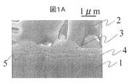
例えば、Cuランドを有する実装基板とSn37Pb共晶はんだボールを有する15mm角のBGA(Ball Grid Arrayの略称)型半導体装置を、Sn37Pb共晶はんだペーストでリフロー接続した接続界面は、図1Aの写真及びその模式図である図1Bに示す様に、実装基板のCuランド1とSn37Pb共晶はんだ2の界面にCu6Sn5化合物3とCu3Sn化合物4と言う2種類の金属間化合物が形成する。さらに、CuとSnの拡散速度の差により、カーケンダルボイド5が発生する場合も有る。
For example, a BGA (abbreviation of B all G rid A rray) type semiconductor device of 15mm x 15mm with a mounting board and Sn37Pb eutectic solder ball having a Cu land, connection interface reflowing connected Sn37Pb eutectic solder paste, Fig. 1A As shown in FIG. 1B, which is a photograph of the above, two types of intermetallic compounds,
また、フラッシュAuめっきを施した無電解Ni−Pめっきランド6を有する実装基板とSn3Ag0.5Cuはんだボールを有する15mm角のBGA型半導体装置を、Sn3Ag0.5Cuはんだペーストでリフロー接続した、接続界面は、図2Aの写真及びその模式図である図2Bに示す様に、実装基板の無電解Ni−Pめっき6とSn3Ag0.5Cuはんだ7の界面にSnNiCu化合物8等の化合物が形成する。さらに、前記化合物と実装基板の無電解Ni−Pめっきの間には、Ni−Pめっきから、Ni成分がはんだと反応した結果、Ni成分が減少し、はんだと反応しないP成分の濃度が高くなった、いわゆるP濃縮層9が形成する。
Further, a mounting substrate having electroless Ni-P plating
上記金属間化合物4、8は固い物質であるため、金属間化合物4、8が厚く成長すると衝撃信頼性を低下する要因となる。また、カーケンダルボイド5が形成する場合、接続面積が減少することで、接続信頼性は低下する。また、P濃縮層9は脆い物質であるため、P濃縮層が厚く成長すると、接続信頼が低下する要因となる。
Since the
前記従来技術により、はんだの残渣は、比較的容易に除去する事が可能である。しかし、金属間化合物は高融点の物質であるため、前記従来技術では、実装基板に劣化が発生する様な高温にしなければ、除去することが出来ない。また、カーケンダルボイド5、P濃縮層9等は、金属間化合物と実装基板ランドの間に形成するため、はんだ残渣だけではなく、金属間化合物も除去しない限り、残存してしまう。
According to the prior art, the solder residue can be removed relatively easily. However, since the intermetallic compound is a substance having a high melting point, the conventional technology cannot be removed unless the temperature is high enough to cause deterioration of the mounting substrate. Further, since the Kirkendall
これら、金属間化合物やボイドや低強度層は、電子部品の取り外し工程、はんだ残渣除去工程、代替部品の、はんだ接続工程で加熱処理が施される度に、逐次形成され、成長していく。したがって、従来技術による、はんだ残渣のみを除去し、代替部品を接続するリペア方法では、代替部品のはんだ接続部は、リペアしない場合に比べ、信頼性の低下した接続状態となる。 These intermetallic compounds, voids, and low-strength layers are successively formed and grown each time heat treatment is performed in the electronic component removal process, the solder residue removal process, and the alternative component solder connection process. Therefore, in the repair method in which only the solder residue is removed and the substitute part is connected according to the conventional technique, the solder connection portion of the substitute part is in a connection state with reduced reliability as compared with the case where the repair part is not repaired.
また、はんだ残渣を除去した後に、金属間化合物が表面に露出する場合が有る。一般に、金属間化合物の、はんだに対する濡れ性は非常に低い。そのため、代替部品を接続する際に、はんだ濡れ不良が発生し、充分な接続信頼性が得られない場合や、はんだ接続自体が達成されない場合も有る。 Moreover, after removing the solder residue, the intermetallic compound may be exposed on the surface. In general, the wettability of the intermetallic compound with respect to the solder is very low. For this reason, when connecting alternative parts, defective solder wetting may occur, and sufficient connection reliability may not be obtained, or solder connection itself may not be achieved.
したがて、本発明の目的は、電子部品と実装基板とを分離する際に、はんだに加えて、実装基板のランド上に形成した、金属間化合物、ボイド及び低強度層等を除去する方法を提供し、代替電子部品の、はんだ接続信頼性を向上させることが可能な電子部品のリペア方法を提供することにある。 Therefore, an object of the present invention is to remove an intermetallic compound, a void, a low-strength layer, and the like formed on the land of the mounting board in addition to the solder when separating the electronic component and the mounting board. It is an object of the present invention to provide an electronic component repair method capable of improving the solder connection reliability of an alternative electronic component.
本発明の特徴は、実装基板に、はんだを介して接続される電子部品のリペア方法において、リペアを必要とする電子部品のはんだ接続部に、金属間化合物層と実装基板ランド間の接続強度が著しく低下するまで、はんだと実装基板のランドとを反応させる熱処理工程と、前記熱処理工程の後に、実装基板から電子部品を取り外す工程において、はんだ接続部が固化している状態で実装基板のランドから、はんだを金属間化合物層と共に機械的に除去する工程とを含む点にある。 The feature of the present invention is that in the method of repairing an electronic component connected to a mounting substrate via solder, the connection strength between the intermetallic compound layer and the mounting substrate land is in the solder connection portion of the electronic component that requires repair. In the heat treatment step for reacting the solder with the land of the mounting substrate until the soldering is significantly reduced, and in the step of removing the electronic component from the mounting substrate after the heat treatment step, the solder connection portion is solidified from the land of the mounting substrate. And a step of mechanically removing the solder together with the intermetallic compound layer.
上記はんだと実装基板のランドとを反応させる熱処理工程における熱処理条件として、加熱温度は、はんだを融点以上でも融点以下でもよい。加熱処理によって、はんだ成分と実装基板上のランドとの反応を進行させ、はんだ接続時に形成された反応生成物である金属間化合物層の厚さを増加させればよい。加熱温度が、はんだ融点以上であれば加熱時間が短くて済み、融点以下であれば加熱時間を延ばせばよい。金属間化合物層の厚さが増加することにより、後工程であるランドから電子部品を除去する工程において、はんだ接続部をランドから容易に剥離することができる。 As a heat treatment condition in the heat treatment step for reacting the solder with the land of the mounting substrate, the heating temperature may be the melting point of the solder or higher or lower than the melting point. The reaction between the solder component and the land on the mounting substrate is advanced by heat treatment, and the thickness of the intermetallic compound layer, which is a reaction product formed at the time of solder connection, may be increased. If the heating temperature is equal to or higher than the melting point of the solder, the heating time may be short, and if it is equal to or lower than the melting point, the heating time may be extended. By increasing the thickness of the intermetallic compound layer, it is possible to easily peel the solder connection portion from the land in the process of removing the electronic component from the land, which is a subsequent process.
また、実装基板から電子部品を取り外す工程において重要なのは、上記熱処理後に、はんだ接続部が固化している状態(はんだを溶融させないこと)で、実装基板のランドから、金属間化合物層と共に、はんだを機械的に除去することである。はんだ接続部に電子部品と実装基板とを引き離すような外力を加えることにより、はんだ接続部とランド間に破断を生じさせ、はんだ残渣を残すことなく、ランドから、はんだ接続部を剥離することにより、電子部品を実装基板から容易に取り外すことができる。 Also, in the process of removing the electronic component from the mounting board, it is important that the solder connection portion is solidified (not to melt the solder) after the heat treatment, and the solder is removed from the land of the mounting board together with the intermetallic compound layer. It is to remove mechanically. By applying an external force that separates the electronic component and the mounting board to the solder connection part, the solder connection part and the land are broken, and the solder connection part is peeled off from the land without leaving a solder residue. The electronic component can be easily removed from the mounting substrate.
本発明によれば、実装基板から電子部品を取り外した後の実装基板上のランド表面は、接続信頼性を低下させる要因である、金属間化合物、ボイド、低強度層が存在しない新生面となる。そのため代替部品の、はんだ接続部は、従来技術によるリペアを行った接続部よりも、高信頼性の接続にすることができる。 According to the present invention, the land surface on the mounting substrate after the electronic component is removed from the mounting substrate becomes a new surface free from intermetallic compounds, voids, and low-strength layers, which are factors that reduce connection reliability. Therefore, the solder connection portion of the alternative part can be connected with higher reliability than the connection portion that has been repaired according to the prior art.
実装基板上のランドから、はんだ接続部を剥離する際の熱処理工程について、本発明の代表的な実施形態を図面にしたがい説明する。図3及び図4は、それぞれ実装基板のランドに接続された、はんだ接続部の熱処理前と熱処理後の拡大断面模式図を示している。 A heat treatment process at the time of peeling a solder connection portion from a land on a mounting substrate will be described with reference to the drawings, with a representative embodiment of the present invention. 3 and 4 are enlarged schematic cross-sectional views before and after heat treatment of the solder connection portions connected to the lands of the mounting substrate, respectively.
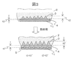
図3(a)は、熱処理前の、はんだ接続部の断面を示しており、実装基板のランド1(Cuランド)上には、金属間化合物層のCu6Sn5化合物3及びCu3Sn化合物4を介して、Sn37Pbはんだ層2が存在する。電子部品は、はんだ層2と接続しているがこの図では省略されている。
FIG. 3A shows a cross-section of the solder connection part before the heat treatment. On the land 1 (Cu land) of the mounting substrate, the intermetallic compound layers of
図3(b)は、熱処理後の、はんだ接続部の断面を示している。これらの図を比較してみると、熱処理後の図3(b)の場合、金属間化合物層のCu6Sn5化合物3及びCu3Sn化合物4の厚さが共に、熱処理前の図3(a)の場合よりも増加していることがわかる。さらに図3(b)の場合、Cuランド1とCu3Sn化合物4との間に多数のボイド(カーケンダルボイド)5が発生している。これら金属間化合物層の膜厚増加及びカーケンダルボイド5の発生が、はんだ接続部がランド1から剥離するのを容易にしている。
FIG. 3B shows a cross section of the solder connection portion after the heat treatment. Comparing these figures, in the case of FIG. 3B after the heat treatment, the thicknesses of the
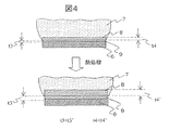
図4(a)は、熱処理前の、はんだ接続部の断面を示しており、実装基板のランド(めっきランド6で、無電解Ni-Pめっき+フラッシュAuめっきの2重めっき)上には、金属間化合物層のSnNiCu化合物8及びP濃縮層9を介して、Sn3Ag0.5Cuはんだ層7が存在する。電子部品は、はんだ層2と接続しているがこの図では省略されている。
FIG. 4A shows a cross section of the solder connection part before the heat treatment. On the land of the mounting substrate (plating
図4(b)は、熱処理後の、はんだ接続部の断面を示している。これらの図を比較してみると、熱処理後の図4(b)の場合、金属間化合物層のSnNiCu化合物8及びP濃縮層9の厚さが共に、熱処理前の図4(a)の場合よりも増加していることがわかる。これら金属間化合物層及びP濃縮層9の膜厚増加が、はんだ接続部が、めっきランド6から剥離するのを容易にしている。
FIG. 4B shows a cross section of the solder connection portion after the heat treatment. Comparing these figures, in the case of FIG. 4B after the heat treatment, the thicknesses of the
以下、本発明の好適な実施例について図面を参照しながら具体的に説明する。 Hereinafter, preferred embodiments of the present invention will be described in detail with reference to the drawings.
<実施例1>
図5及び図6に示した、はんだ接続部の断面拡大図を用いて説明する。先の図1A、図1Bの場合と同様に、Sn37Pb共晶はんだボールを有する15mm角のBGA型半導体装置を、Cuランド1を有する実装基板上に搭載し、Sn37Pb共晶はんだペースト2でリフローすることにより、はんだ接続した。
<Example 1>
The description will be made with reference to the enlarged cross-sectional view of the solder connection portion shown in FIGS. As in the case of FIGS. 1A and 1B, a 15 mm square BGA type semiconductor device having Sn37Pb eutectic solder balls is mounted on a mounting substrate having
次いで局所加熱装置で、はんだ接続部を230℃×120s(sは時間表示の秒)の熱処理条件で加熱した後、室温まで冷却した。この試料の、はんだ接続部(接続界面)の断面拡大写真を図5Aに、その模式図を図5Bに示す。なお、本実施例の熱処理温度は、はんだの融点(183℃)を超えている。 Next, the solder connection part was heated with a local heating device under heat treatment conditions of 230 ° C. × 120 s (s is a time in seconds), and then cooled to room temperature. FIG. 5A shows an enlarged cross-sectional photograph of the solder connection portion (connection interface) of this sample, and FIG. 5B shows a schematic diagram thereof. In addition, the heat processing temperature of a present Example is over melting | fusing point (183 degreeC) of solder.
この図5A及び図5Bを、図1A及び図1Bと比較すれば明らかなように、Cu6Sn5化合物3とCu3Sn化合物4の厚さは、図5A、図5Bの方が厚く成長している。
As is clear from comparison of FIGS. 5A and 5B with FIGS. 1A and 1B, the thicknesses of the
この状態で、BGA型半導体装置と実装基板との間に、スパチュラを差し込んだところ、Cuランド1と、はんだとの間で破断が発生し、それによりランドから、はんだ接続部を剥離し、BGA型半導体装置を容易に取り外すことができた。
In this state, when a spatula is inserted between the BGA type semiconductor device and the mounting substrate, breakage occurs between the
なお、図6は上記の破断部の断面を観察した拡大写真であり、符号10は断面観察のために、破断部に埋め込んだ樹脂層であり、1はランド、3及び4は、はんだとCuランド1との反応生成物(金属間化合物)であるCu6Sn5化合物及びCu3Sn化合物をそれぞれ示している。
6 is an enlarged photograph observing the cross section of the fractured portion.
はんだ接続部の破断は、Cuランド1とCu3Sn化合物4との間で発生しており、図示の通りCuランド1上には、Cu3Sn等の金属間化合物は一切存在せず、Cuランドの新生面が出現している。一方、はんだ側には、Cu3Sn化合物4とCu6Sn5化合物3が付着している。
The breakage of the solder connection portion occurs between the
この、BGA型半導体装置を取り外した後の実装基板のCuランド1上に、Sn37Pb共晶はんだペーストを印刷し、次いでBGA型半導体装置を搭載し、次いで局所リフローを行い、はんだ接続したところ、良好な信頼性を有する、はんだ接続が得られた。
When the Sn37Pb eutectic solder paste is printed on the
本実施例においては、はんだ接続部を230℃×120sの熱処理条件で局所加熱することにより、本発明の目的は達成された。しかし、はんだとランドの反応速度は、ランドを形成する材料の製法や来歴に大きく依存する。したがって、熱処理条件は本実施例の条件に限定されず、使用する実装基板によって、最適な条件(はんだの金属化合物層が生成する条件)を選択する必要が有る。以降の実施例においても、同様である。 In this example, the object of the present invention was achieved by locally heating the solder connection part under the heat treatment condition of 230 ° C. × 120 s. However, the reaction rate between the solder and the land greatly depends on the manufacturing method and history of the material forming the land. Therefore, the heat treatment conditions are not limited to the conditions of this embodiment, and it is necessary to select the optimum conditions (conditions for generating a solder metal compound layer) depending on the mounting substrate to be used. The same applies to the following embodiments.
<実施例2>
Cuランドを有する実装基板に、Sn3Ag0.5Cuはんだボールを有する15mm角のBGA型半導体装置を搭載し、Sn3Ag0.5Cuはんだペーストでリフロー接続した。次いで、はんだ接続部を局所加熱装置で、250℃×120sの条件で熱処理した後、室温まで冷却し、次いで、BGA型半導体装置と実装基板の間にスパチュラを差し込んだところ、Cuランド1と、はんだとの間で破断が発生し、BGA型半導体装置を容易に取り外すことが出来た。
<Example 2>
A 15 mm square BGA type semiconductor device having Sn3Ag0.5Cu solder balls was mounted on a mounting substrate having Cu lands, and reflow-connected with Sn3Ag0.5Cu solder paste. Next, after heat-treating the solder connection portion with a local heating device under the condition of 250 ° C. × 120 s, it was cooled to room temperature, and then a spatula was inserted between the BGA type semiconductor device and the mounting substrate. Breakage occurred with the solder, and the BGA type semiconductor device could be easily removed.
この場合も、実施例1と同様にCuランド1とCu3Sn化合物4との間に明瞭な破断が発生していた。そして、Cuランド1上には、はんだの残留物はなくCuの新生面が出現していた。
In this case as well, a clear fracture occurred between the
このBGA型半導体装置を取り外した後の実装基板のCuランド1上に、Sn37Pb共晶はんだペーストを印刷し、次いで新たなBGA型半導体装置を搭載し、次いで局所リフローを行い、はんだ接続したところ、良好な信頼性を有する、はんだ接続が得られた。
When the Sn37Pb eutectic solder paste is printed on the
<実施例3>
図7及び図8に示した、はんだ接続部の断面拡大図を用いて説明する。
先の図2の場合と同様に、Cuランド表面に無電解Ni−Pめっき+フラッシュAuめっきしたランド6を有する実装基板上に、Sn3Ag0.5Cuはんだボールを有する15mm角のBGA型半導体装置を搭載し、Sn3Ag0.5Cuはんだペースト7でリフロー接続した。
<Example 3>
This will be described with reference to the enlarged cross-sectional view of the solder connection portion shown in FIGS.
As in the case of FIG. 2, a 15 mm square BGA type semiconductor device having a Sn3Ag0.5Cu solder ball is mounted on a mounting substrate having a
次いで、局所加熱装置で、はんだ接続部を250℃×120sの熱処理条件で加熱した後、室温まで冷却した。その時の、はんだ接続部(接続界面)の断面拡大写真を図7Aに、その模式図を図7Bに示す。なお、本実施例の熱処理温度は、はんだの融点(217℃)を超えている。 Next, the solder connection part was heated under a heat treatment condition of 250 ° C. × 120 s with a local heating device, and then cooled to room temperature. FIG. 7A shows an enlarged cross-sectional photograph of the solder connection portion (connection interface) at that time, and FIG. 7B shows a schematic diagram thereof. In addition, the heat processing temperature of a present Example is over melting | fusing point (217 degreeC) of a solder.
SnNiCu化合物8は、はんだ7中に遊離していったため、SnNiCu化合物8の厚さは、図2と変わらないものの、無電解Ni−Pめっきランド6の界面のP濃縮層9(脆い材質)は分厚く成長している。この状態で、BGA型半導体装置と実装基板との間にスパチュラを差し込んだところ、めっきランド6と、はんだとの間で破断が発生し、BGA型半導体装置を容易に取り外すことが出来た。
Since the
図8は上記の破断部の断面を観察した拡大写真である。破断はNi−Pめっきランド6とSnNiCu化合物8の間で発生しており、Ni−Pめっき6上には、SnNiCu化合物8は一切存在せず、また、P濃縮層9も存在しなかった。P濃縮層9は破断させた時に、砕けて、飛散したものと推定する。なお、図8の10は、断面観察のために、破断部に埋め込んだ樹脂層であり、7はSn3Ag0.5Cuはんだをそれぞれ示している。
FIG. 8 is an enlarged photograph observing the cross section of the fracture portion. The fracture occurred between the Ni—
この、BGA型半導体装置を取り外した後の実装基板に、Sn3Ag0.5Cuはんだペーストを印刷し、次いで新たにBGA型半導体装置を搭載し、次いで局所リフローを行い、はんだ接続したところ、良好な信頼性を有する、はんだ接続が得られた。 When the Sn3Ag0.5Cu solder paste is printed on the mounting substrate after the BGA type semiconductor device is removed, then the BGA type semiconductor device is newly mounted, and then a local reflow is performed and solder connection is performed. A solder connection having was obtained.
<実施例4>
実施例1と同様に、Cuランドを有する実装基板とSn37Pb共晶はんだボールを有する15mm角のBGA型半導体装置とを、Sn37Pb共晶はんだペーストでリフロー接続した。次いで、はんだ接続部を局所加熱装置で、230℃×120sの熱処理条件で加熱した後、室温まで冷却した。
<Example 4>
Similar to Example 1, a mounting substrate having Cu lands and a 15 mm square BGA type semiconductor device having Sn37Pb eutectic solder balls were reflow-connected with Sn37Pb eutectic solder paste. Next, the solder connection part was heated with a local heating device under heat treatment conditions of 230 ° C. × 120 s, and then cooled to room temperature.
次いで、BGA型半導体装置と実装基板との間にスパチュラを差し込んだところ、Cuランド1と、はんだとの間で破断したバンプとBGA型半導体装置側の接続界面で破断したバンプとが混在する破断が発生した。
Next, when a spatula is inserted between the BGA type semiconductor device and the mounting substrate, the bumps broken between the
実施例1のBGA型半導体装置は、電気Niめっきに、はんだバンプを形成したものであるのに対し、本実施例のBGA型半導体装置は、無電解Ni−Pめっきに、はんだバンプを形成したものであったため、BGA側と実装基板側の両者のはんだ接続界面が、同様に接続強度が劣化したため、ランダムに破断が発生したためである。 The BGA type semiconductor device of Example 1 is one in which solder bumps are formed on electric Ni plating, whereas the BGA type semiconductor device in this example has solder bumps formed on electroless Ni-P plating. This is because the solder connection interface on both the BGA side and the mounting substrate side similarly deteriorated in connection strength, and therefore, fracture occurred randomly.
そこで、実装基板側に残った、はんだバンプを、バンプせん断試験機を用い、5mm/secの速度で、せん断応力を与えたところ、はんだバンプが除去され、実装基板側にはCuランドの新生面が出現した。このBGA型半導体装置及び基板に残存した、はんだバンプを取り外した後の実装基板に、Sn37Pb共晶はんだペーストを印刷し、次いでBGA型半導体装置を搭載し、次いで局所リフローを行い、はんだ接続したところ、良好な信頼性を有する、はんだ接続が得られた。 Therefore, when the solder bumps remaining on the mounting substrate side were subjected to a shear stress at a speed of 5 mm / sec using a bump shear tester, the solder bumps were removed, and a new surface of the Cu land was formed on the mounting substrate side. Appeared. This BGA type semiconductor device and the substrate remaining on the mounting board after removing the solder bumps are printed with Sn37Pb eutectic solder paste, then the BGA type semiconductor device is mounted, and then local reflow is performed and soldering is performed. A solder connection with good reliability was obtained.
本実施例では。実装基板側に残った、はんだバンプに、せん断応力を与えるために、バンプせん断試験機を使用したが、同様の応力を与える事が可能な如何なる手法を用いて、はんだバンプ及び、金属間化合物層を除去しても良い。 In this example. A bump shear tester was used to apply a shear stress to the solder bumps remaining on the mounting board side, but using any method capable of applying the same stress, the solder bump and intermetallic compound layer May be removed.
<実施例5>
実施例1に記載の、BGA型半導体装置を搭載した実装基板を、230℃×60sの熱処理条件で加熱し、はんだが溶融した状態で、BGA型半導体装置を取り外した。さらに、120s加熱を続けた後、室温まで冷却した。
<Example 5>
The mounting substrate on which the BGA type semiconductor device described in Example 1 was mounted was heated under heat treatment conditions of 230 ° C. × 60 s, and the BGA type semiconductor device was removed while the solder was melted. Further, the heating for 120 s was continued, and then cooled to room temperature.
この時、実装基板のCuランド上には、ランドと、はんだとの反応生成物である金属間化合物と、はんだ残渣とが存在した。次いで、実施例4と同様に、バンプせん断試験機を用い、5mm/secの速度で、せん断応力を与えたところ、はんだ残渣と金属間化合物が除去され、Cuランド上には、Cuの新生面が出現した。 At this time, lands, an intermetallic compound that is a reaction product of solder, and solder residues were present on the Cu lands of the mounting substrate. Next, as in Example 4, when a shear stress was applied using a bump shear tester at a speed of 5 mm / sec, the solder residue and the intermetallic compound were removed, and a new surface of Cu was formed on the Cu land. Appeared.
次いで、Sn37Pb共晶はんだペーストを印刷し、次いでBGA型半導体装置を新たに搭載し、次いで局所リフローを行い、はんだ接続したところ、良好な信頼性を有する、はんだ接続が得られた。 Next, when Sn37Pb eutectic solder paste was printed, then a BGA type semiconductor device was newly mounted, then local reflow was performed, and solder connection was performed, solder connection with good reliability was obtained.
本発明は、製造工程内、市場を問わず、不良が発生した電子部品のリペアに利用可能である。 INDUSTRIAL APPLICABILITY The present invention can be used for repairing defective electronic components regardless of the manufacturing process or market.
<実施例6>
実施例1に記載の、BGA型半導体装置を搭載した実装基板を、Sn37Pb共晶はんだの融点(183℃)以下の温度である170℃で、5分間加熱した後、室温まで冷却し、次いで、BGA型半導体装置と実装基板の間にスパチュラを差し込んだところ、Cuランド1と、はんだの間で破断が発生し、BGA型半導体装置を取り外すことができた。
<Example 6>
The mounting board on which the BGA type semiconductor device described in Example 1 is mounted is heated at 170 ° C., which is lower than the melting point (1833 ° C.) of Sn37Pb eutectic solder, for 5 minutes, then cooled to room temperature, When a spatula was inserted between the BGA type semiconductor device and the mounting substrate, breakage occurred between the
この時の破断は、実施例1と同様に、Cuランド1とCu3Sn化合物4との間で発生していた。そして、Cuランド1上には、Cuの新生面が出現していた。
The breakage at this time occurred between the
この、BGA型半導体装置を取り外した後のCuランド1上に、Sn37Pb共晶はんだペーストを印刷し、次いで、BGA型半導体装置を搭載し、次いで局所リフローを行い、はんだ接続したところ、良好な信頼性を有する、はんだ接続が得られた。
When the Sn 37 Pb eutectic solder paste is printed on the
本実施例では、熱処理時間を170℃、5分間としたが、本発明はこれに限定されるものではない。 In this embodiment, the heat treatment time is 170 ° C. and 5 minutes, but the present invention is not limited to this.
処理温度が高いほど、はんだとランドの反応によるCuSn化合物の生成速度は速いので、必要な処理時間は短い。作業上、熱処理時間は短いことが望ましい。実施例1、4、5記載のSn37Pb共晶はんだや、実施例2、3記載のSn3Ag0.5Cuに代表される、中温鉛フリーはんだでは、はんだの融点−20℃以上の温度が望ましい。本実施例において、Sn37Pb共晶はんだの融点(183℃)より、23℃低い160℃で処理した場合、Cuランド1とCu3Sn化合物4との間で破断を発生させるのに約10分の処理時間が必要で、リペア効率が著しく低下し、好ましくなかった。
The higher the processing temperature, the faster the CuSn compound generation rate due to the reaction between the solder and the land, and the shorter the processing time required. In terms of work, it is desirable that the heat treatment time be short. In the medium temperature lead-free solder represented by Sn37Pb eutectic solder described in Examples 1, 4, and 5 and Sn3Ag0.5Cu described in Examples 2 and 3, the temperature of the melting point of the solder is −20 ° C. or higher. In this example, when processing at 160 ° C., which is 23 ° C. lower than the melting point (183 ° C.) of the Sn37Pb eutectic solder, a processing time of about 10 minutes is required to generate a fracture between the
実施例1〜5記載の条件で、リペアを行う場合、リペアを実施するBGA型半導体装置近傍に、はんだ接続された他の電子部品の、はんだ接続部も溶融し、リペアの必要のない電子部品の、はんだ接続強度も著しく低下させる可能性がある。そこで、はんだの融点以下の温度で、BGA型半導体装置の熱処理を行わなければならない場合がある。本実施例では、BGA型半導体装置近傍の電子部品の、はんだ接続部が溶融する可能性は無いため上記した課題を回避できる。 When repair is performed under the conditions described in the first to fifth embodiments, an electronic component that does not need to be repaired by melting a solder connection portion of another electronic component that is solder-connected in the vicinity of the BGA type semiconductor device to be repaired There is also a possibility that the solder connection strength will be significantly reduced. Therefore, there are cases where the heat treatment of the BGA type semiconductor device must be performed at a temperature below the melting point of the solder. In this embodiment, since there is no possibility that the solder connection portion of the electronic component near the BGA type semiconductor device is melted, the above-described problems can be avoided.
1…Cuランド、
2…Sn37Pbはんだ、
3…Cu6Sn5化合物、
4…Cu3Sn化合物、
5…カーケンダルボイド、
6…無電解Ni−Pめっき+フラッシュAuめっきランド、
7…Sn3Ag0.5Cuはんだ、
8…SnNiCu化合物、
9…P濃縮層、
10…断面観察のために用いた埋め込み樹脂。
1 ... Cu Land,
2 ... Sn37Pb solder,
3 ... Cu6Sn5 compound,
4 ... Cu3Sn compound,
5 ... Kirkendall void,
6 ... Electroless Ni-P plating + Flash Au plating land,
7 ... Sn3Ag0.5Cu solder,
8 ... SnNiCu compound,
9 ... P concentrated layer,
10: Embedded resin used for cross-sectional observation.
Claims (3)
前記電子部品をランドから取り外す工程においては、前記電子部品とランドとの、はんだ接続部を一定時間加熱し、はんだと実装基板のランドとを反応させることにより、はんだ接続時に形成された金属間化合物層と実装基板ランド間の接続強度を、ランドとランド下地の基板間の接続強度よりも小さくする熱処理工程と、
前記熱処理工程の後に、前記はんだ接続部を、はんだの溶融温度よりも低い温度に保持し、はんだ接続部が固化している状態で、前記電子部品と前記実装基板との間に外力を加えて前記電子部品を前記実装基板から引き離すことにより、はんだ接続部の金属間化合物層とランドとの間に破断を生じさせ、実装基板上に残った、はんだを金属間化合物層と共にランドから除去し、実装基板上に、はんだ残渣を残さずに電子部品をランドから取り外す工程とを含むことを特徴とする電子部品のリペア方法。 A method of repairing an electronic component, comprising: a step of removing an electronic component solder-connected to the land of the mounting substrate from the land; and a step of soldering and attaching an alternative electronic component to the land of the mounting substrate.
In the step of removing the electronic component from the land, an intermetallic compound formed at the time of solder connection by heating a solder connection portion between the electronic component and the land for a certain period of time and reacting the solder with the land of the mounting substrate. A heat treatment step for making the connection strength between the layer and the mounting substrate land smaller than the connection strength between the land and the substrate of the land base,
After the heat treatment step, the solder connection portion is held at a temperature lower than the melting temperature of the solder, and an external force is applied between the electronic component and the mounting substrate in a state where the solder connection portion is solidified. By pulling the electronic component away from the mounting substrate, a break occurs between the intermetallic compound layer and the land of the solder connection portion, and the solder remaining on the mounting substrate is removed from the land together with the intermetallic compound layer, And a step of removing the electronic component from the land without leaving a solder residue on the mounting substrate.
In the heat treatment step of heating the solder connection portion between the electronic component and the land in the step of removing the electronic component from the land for a predetermined time, the heating temperature of the solder connection portion is performed at a temperature lower than the melting point of the solder. The method of repairing an electronic component according to claim 1.
Priority Applications (1)
| Application Number | Priority Date | Filing Date | Title |
|---|---|---|---|
| JP2004368981A JP2006179556A (en) | 2004-12-21 | 2004-12-21 | Electronic component repair method |
Applications Claiming Priority (1)
| Application Number | Priority Date | Filing Date | Title |
|---|---|---|---|
| JP2004368981A JP2006179556A (en) | 2004-12-21 | 2004-12-21 | Electronic component repair method |
Publications (1)
| Publication Number | Publication Date |
|---|---|
| JP2006179556A true JP2006179556A (en) | 2006-07-06 |
Family
ID=36733401
Family Applications (1)
| Application Number | Title | Priority Date | Filing Date |
|---|---|---|---|
| JP2004368981A Pending JP2006179556A (en) | 2004-12-21 | 2004-12-21 | Electronic component repair method |
Country Status (1)
| Country | Link |
|---|---|
| JP (1) | JP2006179556A (en) |
Cited By (1)
| Publication number | Priority date | Publication date | Assignee | Title |
|---|---|---|---|---|
| JP2015050286A (en) * | 2013-08-30 | 2015-03-16 | 株式会社東芝 | Peeling apparatus and peeling method |
-
2004
- 2004-12-21 JP JP2004368981A patent/JP2006179556A/en active Pending
Cited By (1)
| Publication number | Priority date | Publication date | Assignee | Title |
|---|---|---|---|---|
| JP2015050286A (en) * | 2013-08-30 | 2015-03-16 | 株式会社東芝 | Peeling apparatus and peeling method |
Similar Documents
| Publication | Publication Date | Title |
|---|---|---|
| US6574859B2 (en) | Interconnection process for module assembly and rework | |
| JPH08255971A (en) | Method for forming a temporary bond between a semiconductor die and a substrate | |
| JP6088950B2 (en) | Stud bump structure and manufacturing method thereof | |
| JP6280875B2 (en) | Method for forming solder bump and solder bump | |
| CN1537327A (en) | Flip-chip interconnect using no-clean flux | |
| KR100567611B1 (en) | Solder for use on surfaces coated with nickel by electroless plating | |
| JP2012157873A (en) | Solder, soldering method and semiconductor device | |
| JPH10163213A (en) | Semiconductor device manufacturing method and semiconductor device mounting method | |
| JP5031677B2 (en) | Manufacturing method of bonded structure | |
| JP2001332583A (en) | Semiconductor chip mounting method | |
| TW200819012A (en) | Mounting structure | |
| JP3400408B2 (en) | Flip chip mounting method | |
| JP2009009994A (en) | Semiconductor device and manufacturing method thereof | |
| JP3998484B2 (en) | How to connect electronic components | |
| JP2007128982A (en) | Semiconductor bump connection structure and manufacturing method thereof | |
| JP2009277777A (en) | Solder ball loading method and member for mounting electronic component | |
| JP2002001520A (en) | Soldering method and soldering structure | |
| JP2006179556A (en) | Electronic component repair method | |
| JP3377411B2 (en) | Flip chip mounting structure | |
| JP2003223945A (en) | Au-Ge based brazing lead pin | |
| JPH10335805A (en) | Electronic component mounting method | |
| JP2001156441A (en) | Repair method for CSP / BGA | |
| JP2008218483A (en) | Semiconductor device and manufacturing method thereof | |
| JP3722096B2 (en) | Mounting board manufacturing method | |
| JP2001156095A (en) | Electrode, semiconductor device and manufacturing method |