JP2006093286A - Process for manufacturing multilayer ceramic electronic component - Google Patents
Process for manufacturing multilayer ceramic electronic component Download PDFInfo
- Publication number
- JP2006093286A JP2006093286A JP2004274938A JP2004274938A JP2006093286A JP 2006093286 A JP2006093286 A JP 2006093286A JP 2004274938 A JP2004274938 A JP 2004274938A JP 2004274938 A JP2004274938 A JP 2004274938A JP 2006093286 A JP2006093286 A JP 2006093286A
- Authority
- JP
- Japan
- Prior art keywords
- conductor pattern
- electronic component
- ceramic layer
- multilayer ceramic
- manufacturing
- Prior art date
- Legal status (The legal status is an assumption and is not a legal conclusion. Google has not performed a legal analysis and makes no representation as to the accuracy of the status listed.)
- Pending
Links
Images


Landscapes
- Ceramic Capacitors (AREA)
- Production Of Multi-Layered Print Wiring Board (AREA)
- Manufacturing Of Printed Wiring (AREA)
Abstract
Description
本発明は、携帯電話機等の小型の電子機器に装備される各種電子回路を構成するための積層セラミック電子部品の製造方法に関するものである。 The present invention relates to a method for manufacturing a multilayer ceramic electronic component for constituting various electronic circuits equipped in a small electronic device such as a mobile phone.
近年、携帯電話機等の小型の電子機器においては、小型化に対する要求が益々厳しくなってきており、この様な状況において、機器を構成する複数の回路素子を1チップの積層セラミック電子部品に集積化して、該積層セラミック電子部品をメイン基板に実装することが行なわれている。 In recent years, in small electronic devices such as mobile phones, the demand for downsizing has become more and more severe. In such a situation, a plurality of circuit elements constituting the device are integrated into a single-chip multilayer ceramic electronic component. Thus, the multilayer ceramic electronic component is mounted on a main board.
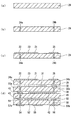
図4(a)〜(e)は、従来の積層セラミック電子部品(101)の一連の製造工程を示している。図4(e)に示す如く、該積層セラミック電子部品(101)は、4層のセラミック層(6)(7)(8)(9)の積層構造を有している。
該積層セラミック電子部品(101)は、図4(a)〜(c)に示す如く、4層のセラミック層(6)(7)(8)(9)となる4枚のグリーンシート(69)(79)(89)(99)にそれぞれ所定の導体パターンを形成する導体パターン形成工程と、該導体パターン形成工程を経て得られる4枚のグリーンシート(69)(79)(89)(99)を図4(d)に示す如く積層し、積層体を作製する積層体作製工程と、図4(e)に示す如く、該積層体作製工程を経て得られる積層体に焼成を施す焼成工程とを経て作製される。
尚、図4(a)〜(c)は、前記導体パターン形成工程を、最上層の第1セラミック層(6)となる第1グリーンシート(69)について示したものである。
図4(a)に示す如く、先ず、第1グリーンシート(69)を用意し、次に、図4(b)に示す如く、第1グリーンシート(69)の所定位置に貫通孔(64a)(64b)を開設した後、図4(c)に示す如く、貫通孔(64a)(64b)に導体材料を充填して垂直線路を形成すると共に、第1グリーンシート(69)の表面に導体材料を印刷して、所定の導体パターン(61)(62)(63)を形成する。
同様にして、第2乃至第4セラミック層(7)(8)(9)となる第2乃至第4グリーンシート(79)(89)(99)にも、それぞれ所定の導体パターンと垂直線路を形成する。
4A to 4E show a series of manufacturing steps of the conventional multilayer ceramic electronic component (101). As shown in FIG. 4 (e), the multilayer ceramic electronic component (101) has a multilayer structure of four ceramic layers (6), (7), (8) and (9).
The multilayer ceramic electronic component (101) is composed of four green sheets (69) that form four ceramic layers (6), (7), (8), and (9) as shown in FIGS. (79) (89) (99) Conductive pattern forming step for forming a predetermined conductive pattern on each, and four green sheets (69) (79) (89) (99) obtained through the conductive pattern forming step 4 (d), and a laminate manufacturing step for manufacturing the laminate, and a firing step for firing the laminate obtained through the laminate manufacturing step as shown in FIG. 4 (e). It is produced through.
4A to 4C show the conductor pattern forming step for the first
As shown in FIG. 4 (a), first, a first green sheet (69) is prepared, and then, as shown in FIG. 4 (b), a through hole (64a) is formed at a predetermined position of the first green sheet (69). After opening (64b), as shown in FIG. 4 (c), the through holes (64a) and (64b) are filled with a conductor material to form a vertical line, and the conductor on the surface of the first green sheet (69). The material is printed to form predetermined conductor patterns (61) (62) (63).
Similarly, the second to fourth green sheets (79), (89), and (99) to be the second to fourth ceramic layers (7), (8), and (9) are respectively provided with predetermined conductor patterns and vertical lines. Form.
次の積層体作製工程では、前記導体パターン形成工程を経て得られた第1乃至第4グリーンシート(69)(79)(89)(99)を図4(d)に示す如く順に積み重ねて、積層体を作製する。その後、図4(e)に示す焼成工程にて、該積層体に熱圧着及び焼成を施して一体化する。この様にして積層セラミック電子部品(101)が作製されることになる。 In the next laminate manufacturing step, the first to fourth green sheets (69) (79) (89) (99) obtained through the conductor pattern forming step are sequentially stacked as shown in FIG. A laminate is produced. Thereafter, in the firing step shown in FIG. 4 (e), the laminate is integrated by thermocompression bonding and firing. In this way, the multilayer ceramic electronic component (101) is manufactured.
しかしながら、図4(e)に示す焼成工程において、第1セラミック層(6)の表面に形成された第1の導体パターン(61)と第2セラミック層(7)の表面に形成された第2の導体パターン(71)とが、図示の如く微細な短絡線路(65)により接続されて、短絡不良が発生することがあった。 However, in the firing step shown in FIG. 4 (e), the first conductor pattern (61) formed on the surface of the first ceramic layer (6) and the second conductor layer formed on the surface of the second ceramic layer (7). The conductor pattern (71) is connected by a fine short-circuit line (65) as shown in the figure, resulting in a short-circuit failure.
発明者は上述の短絡不良が発生する条件を分析したところ、両導体パターン(61)(71)が互いに電気的に絶縁されており、且つ、両導体パターン(61)(71)が上下方向に重なって、互いにオーバーラップする領域を有している場合に短絡不良が発生することを見出した。
上述の短絡不良は、例えば、図4(e)に示す如く互いに電気的に接続された第1セラミック層(6)上の導体パターン(63)と第2セラミック層(7)上の導体パターン(72)との間では発生しない。即ち、両導体パターン(63)(72)が上下方向に重なって、互いにオーバーラップする領域を有していても、貫通孔(64b)に形成された垂直線路によって互いに電気的に接続されていれば、短絡不良は発生しないのである。
The inventor analyzed the conditions under which the above short-circuit failure occurred, and as a result, both the conductor patterns (61) and (71) were electrically insulated from each other, and both the conductor patterns (61) and (71) were vertically aligned. It has been found that short-circuit defects occur when overlapping and having overlapping regions.
The short-circuit failure described above is caused by, for example, the conductor pattern (63) on the first ceramic layer (6) and the conductor pattern (2) on the second ceramic layer (7) that are electrically connected to each other as shown in FIG. It does not occur with 72). That is, even if the two conductor patterns (63) and (72) overlap each other in the vertical direction and overlap each other, they are electrically connected to each other by the vertical line formed in the through hole (64b). In this case, no short circuit failure occurs.
そこで、発明者は短絡不良の原因を、焼成工程において発生する両導体パターン(61)(71)間の電位差によるものと推測した。
即ち、焼成工程において、温度上昇に伴う焦電効果及び圧着による圧電効果によって、誘電体である第1セラミック層(6)に分極が生じ、該分極に伴って、第1セラミック層(6)を挟んで互いに対向する第1及び第2の導体パターン(61)(71)が帯電して、両導体パターン(61)(71)間に電位差が生じることになる。該電位差に起因して微細な短絡線路(65)が形成され、短絡不良が発生すると推測されるのである。
Therefore, the inventor speculated that the cause of the short-circuit failure was due to the potential difference between the two conductor patterns (61) and (71) generated in the firing process.
That is, in the firing step, polarization occurs in the first ceramic layer (6), which is a dielectric, due to the pyroelectric effect accompanying the temperature rise and the piezoelectric effect due to the pressure bonding, and the first ceramic layer (6) is formed along with the polarization. The first and second conductor patterns (61) and (71) that are opposed to each other are charged, and a potential difference is generated between the conductor patterns (61) and (71). It is estimated that a fine short circuit line (65) is formed due to the potential difference and a short circuit failure occurs.
ところで、高温高湿条件下において、微小な間隔で形成された配線間を導体材料が移動して、該配線間が短絡してしまうマイグレーション現象が知られており、マイグレーション現象の発生を防止すべく種々の導体材料が提案されている(特許文献1参照)。
しかしながら、マイグレーション現象が発生し難い導体材料を用いたとしても、上述の短絡不良の発生を防止することが充分ではなかった。
そこで、従来の積層セラミック電子部品の製造においては、セラミック層を挟んで対向する2つの導体パターンがセラミック層の積層方向に重ならない様に配置し、或いはセラミック層の厚さを一定以上の厚さに形成する等の設計上の対策を施すことにより、短絡不良の発生を防止していた。
しかしながら、この様な設計上の対策のために集積度が低下して、積層セラミック電子部品が大型化してしまう問題があった。
そこで、本発明の目的は、積層セラミック電子部品の大型化を招くことなく、短絡不良の発生を防止することが出来る積層セラミック電子部品の製造方法を提供することである。
However, even when a conductive material that hardly causes the migration phenomenon is used, it is not sufficient to prevent the occurrence of the short-circuit failure described above.
Therefore, in the manufacture of conventional multilayer ceramic electronic components, two conductor patterns facing each other across the ceramic layer are arranged so as not to overlap in the stacking direction of the ceramic layer, or the thickness of the ceramic layer is a certain thickness or more. The occurrence of a short circuit failure was prevented by taking measures on the design such as forming on the surface.
However, due to such design measures, there is a problem that the degree of integration decreases and the multilayer ceramic electronic component becomes large.
Accordingly, an object of the present invention is to provide a method for manufacturing a multilayer ceramic electronic component capable of preventing the occurrence of a short circuit failure without increasing the size of the multilayer ceramic electronic component.
本発明の対象とする積層セラミック電子部品は、所定の導体パターンが形成された複数のセラミック層の積層構造を有し、最上層のセラミック層と最下層のセラミック層の内、少なくとも一方のセラミック層には、外側に露出する表面に、互いに電気的に絶縁された第1の導体パターンと第2の導体パターンとが形成されると共に、該セラミック層と直接に重なるセラミック層の表面には第3の導体パターンが形成され、該第3の導体パターンは、前記第2の導体パターンと電気的に接続されると共に、前記第1の導体パターンとは電気的に絶縁されている。 本発明に係る積層セラミック電子部品の製造方法は、前記複数のセラミック層となる複数枚のグリーンシートにそれぞれ所定の導体パターンを形成する導体パターン形成工程と、該導体パターン形成工程を経て得られる複数枚のグリーンシートを積層して積層体を作製する積層体作製工程と、該積層体作製工程を経て得られる積層体に焼成を施す焼成工程とを有している。
前記導体パターン形成工程では、前記一方のセラミック層となるグリーンシートの表面に、前記第1の導体パターンと第2の導体パターンとを形成すると共に、第1の導体パターンと第2の導体パターンとを互いに電気的に接続する接続線路を形成し、前記焼成工程の後、前記接続線路の一部若しくは全部を除去して、第1の導体パターンと第2の導体パターンとを互いに電気的に絶縁する絶縁処理工程を実施する。
A multilayer ceramic electronic component which is an object of the present invention has a multilayer structure of a plurality of ceramic layers on which a predetermined conductor pattern is formed, and at least one of the uppermost ceramic layer and the lowermost ceramic layer The first conductor pattern and the second conductor pattern that are electrically insulated from each other are formed on the surface exposed to the outside, and a third layer is formed on the surface of the ceramic layer that directly overlaps the ceramic layer. The third conductor pattern is electrically connected to the second conductor pattern and electrically insulated from the first conductor pattern. The manufacturing method of the multilayer ceramic electronic component according to the present invention includes a conductor pattern forming step of forming a predetermined conductor pattern on each of the plurality of green sheets to be the plurality of ceramic layers, and a plurality of conductor patterns obtained through the conductor pattern forming step. It has the laminated body preparation process which laminates | stacks the green sheet of 1 sheet, and produces a laminated body, and the baking process which bakes the laminated body obtained through this laminated body preparation process.
In the conductor pattern forming step, the first conductor pattern and the second conductor pattern are formed on the surface of the green sheet serving as the one ceramic layer, and the first conductor pattern and the second conductor pattern are formed. Are connected to each other, and after the firing step, a part or all of the connection lines are removed to electrically insulate the first conductor pattern and the second conductor pattern from each other. An insulating treatment process is performed.
上記本発明の積層セラミック電子部品の製造方法によれば、導体パターン形成工程にて、前記第1の導体パターンと第2の導体パターンは、前記接続線路を介して互いに電気的に接続される。
次の積層体作製工程にて作製される積層体の状態において、前記第2の導体パターンと第3の導体パターンとが互いに電気的に接続され、これによって前記第1の導体パターンと第3の導電パターンとが、前記接続線路及び第2の導体パターンを介して互いに電気的に接続されることになる。
この結果、次の焼成工程中に、仮に前記第1の導体パターンと第3の導体パターンとに挟まれたセラミック層に分極が生じ、前記第1の導体パターンと第3の導体パターンとが一時的に異なる電位に帯電したとしても、前記第1の導体パターンと第3の導体パターンとの間で電荷が移動して、前記第1の導体パターンと第3の導体パターンとは同電位に保たれる。従って、前記第1の導体パターンと第3の導体パターンの間に電位差が生じることはない。これによって、短絡不良の発生を防止することが出来る。
更に、次の絶縁処理工程にて前記接続線路の一部或いは全部を除去することにより、前記第1導体パターンと前記第2の導電パターンとが電気的に絶縁されて、所望の積層セラミック電子部品が完成することになる。
According to the method for manufacturing a multilayer ceramic electronic component of the present invention, in the conductor pattern forming step, the first conductor pattern and the second conductor pattern are electrically connected to each other via the connection line.
In the state of the laminate produced in the next laminate production process, the second conductor pattern and the third conductor pattern are electrically connected to each other, whereby the first conductor pattern and the third conductor pattern are electrically connected to each other. A conductive pattern is electrically connected to each other via the connection line and the second conductor pattern.
As a result, during the next firing step, the ceramic layer sandwiched between the first conductor pattern and the third conductor pattern is polarized, and the first conductor pattern and the third conductor pattern are temporarily separated. Even if charged to different potentials, the charge moves between the first conductor pattern and the third conductor pattern, and the first conductor pattern and the third conductor pattern are kept at the same potential. Be drunk. Therefore, there is no potential difference between the first conductor pattern and the third conductor pattern. Thereby, the occurrence of short circuit failure can be prevented.
Furthermore, the first conductor pattern and the second conductive pattern are electrically insulated by removing a part or all of the connection line in the next insulation processing step, so that a desired multilayer ceramic electronic component is obtained. Will be completed.
上記本発明の積層セラミック電子部品の製造方法によれば、従来のような設計上の対策を施すことなく短絡不良の発生を防止することが出来る。又、従来は短絡不良が発生していた領域、即ち前記第1の導体パターンと少なくとも一部がオーバーラップすることとなる領域に、前記第3の導体パターンを形成することが可能となるので、これによって、積層セラミック電子部品の集積度が向上し、積層セラミック電子部品の小型化を図ることが出来る。 According to the method for manufacturing a multilayer ceramic electronic component of the present invention, it is possible to prevent occurrence of a short circuit failure without taking a conventional design measure. In addition, since it is possible to form the third conductor pattern in a region where a short-circuit failure has conventionally occurred, that is, a region where at least part of the first conductor pattern overlaps, As a result, the degree of integration of the multilayer ceramic electronic component is improved, and the multilayer ceramic electronic component can be miniaturized.
具体的方法において、前記絶縁処理工程では、接続線路の一部若しくは全部を削って除去する。
該具体的方法においては、前記接続線路は、積層セラミック電子部品の外側に露出する表面に形成されているので、外部から該接続線路の位置を確認しながら、その一部若しくは全部を削って除去することが出来る。
In a specific method, in the insulation treatment step, part or all of the connection line is removed by shaving.
In the specific method, since the connection line is formed on the surface exposed to the outside of the multilayer ceramic electronic component, a part or all of the connection line is removed by removing while confirming the position of the connection line from the outside. I can do it.
又、具体的方法において、前記導体パターン形成工程では、前記一方のセラミック層となるグリーンシートに垂直の貫通孔を開設した後、該貫通孔に導体材料を充填して垂直線路を形成し、該垂直線路によって前記第2の導体パターンと第3の導体パターンとを互いに電気的に接続する。
該具体的方法によれば、前記積層体作製工程を経て作製した積層体の状態において、前記一方のセラミック層となるグリーンシートと、表面に前記第3の導体パターンが形成されたグリーンシートとが重なって、前記垂直線路と前記第3の導体パターンとが互いに接触することにより、前記第2の導体パターンと第3の導体パターンとが前記垂直線路を介して互いに電気的に接続されることになる。
Further, in a specific method, in the conductor pattern forming step, a vertical through hole is formed in the green sheet to be the one ceramic layer, and then the through hole is filled with a conductor material to form a vertical line, The second conductor pattern and the third conductor pattern are electrically connected to each other by a vertical line.
According to the specific method, in the state of the laminate produced through the laminate production step, a green sheet that becomes the one ceramic layer, and a green sheet on which the third conductor pattern is formed are formed. When the vertical line and the third conductor pattern come into contact with each other, the second conductor pattern and the third conductor pattern are electrically connected to each other through the vertical line. Become.
本発明の積層セラミック電子部品の製造方法によれば、積層セラミック電子部品の大型化を招くことなく、短絡不良の発生を防止することが出来る。 According to the method for manufacturing a multilayer ceramic electronic component of the present invention, it is possible to prevent occurrence of a short circuit failure without increasing the size of the multilayer ceramic electronic component.
以下、本発明の実施の形態につき、図面に沿って具体的に説明する。
本発明に係る積層セラミック電子部品(1)は、図2(b)に示す如く、4層のセラミック層(2)(3)(4)(5)の積層構造を有している。
図2(b)及び図3(b)に示す如く、最上層の第1セラミック層(2)の表面には、第1導体パターン(21)及び第2導体パターン(22)を含む所定の導体パターンが形成されており、第2導体パターン(22)と第1セラミック層(2)に接する第2セラミック層(3)の表面に形成された第3導体パターン(31)とは、導体材料が充填された貫通孔(24a)を介して互いに電気的に接続されている。一方、第1導体パターン(21)は、第2導体パターン(22)及び第3導体パターン(31)の何れとも接続されず、電気的に絶縁状態にあり、且つ、第3導体パターン(31)と上下方向に重なって、互いにオーバーラップする領域に形成されている。
各セラミック層(2)(3)(4)(5)は、例えば5mm角の平板形状を呈し、各セラミック層(2)(3)(4)(5)の厚さは、例えば50μmに形成されている。又、各導体パターンの厚さは、例えば10〜20μmに形成されている。
Hereinafter, embodiments of the present invention will be specifically described with reference to the drawings.
The multilayer ceramic electronic component (1) according to the present invention has a multilayer structure of four ceramic layers (2), (3), (4) and (5) as shown in FIG. 2 (b).
As shown in FIGS. 2B and 3B, a predetermined conductor including a first conductor pattern (21) and a second conductor pattern (22) is formed on the surface of the uppermost first ceramic layer (2). The third conductor pattern (31) formed on the surface of the second ceramic layer (3) in contact with the second conductor pattern (22) and the first ceramic layer (2) is formed of a conductive material. They are electrically connected to each other through the filled through holes (24a). On the other hand, the first conductor pattern (21) is not connected to any of the second conductor pattern (22) and the third conductor pattern (31), is electrically insulated, and the third conductor pattern (31). And are overlapped with each other in the vertical direction and overlap each other.
Each ceramic layer (2), (3), (4) and (5) has a flat plate shape of 5 mm square, for example, and the thickness of each ceramic layer (2), (3), (4) and (5) is, for example, 50 μm. Has been. Moreover, the thickness of each conductor pattern is formed to 10-20 micrometers, for example.
上記本発明の積層セラミック電子部品(1)の製造工程においては、先ず、導体パターン形成工程にて、第1乃至第4セラミック層(2)(3)(4)(5)となる第1乃至第4グリーンシート(29)(39)(49)(59)にそれぞれ所定の導体パターンを形成する。
図1(a)〜(c)は、第1セラミック層(2)となる第1グリーンシート(29)についての導体パターン形成工程を示したものである。
図1(a)に示す如く、先ず、第1グリーンシート(29)を用意し、次に、図1(b)に示す如く、第1グリーンシート(29)の所定位置に貫通孔(24a)(24b)を開設する。その後、図1(c)に示す如く、貫通孔(24a)(24b)に導体材料を充填して垂直線路を形成すると共に、第1グリーンシート(29)の表面に導体材料を印刷して、図1(c)及び図3(a)に示す如く、第1導体パターン(21)及び第2導体パターン(22)を含む所定の導体パターンを形成すると共に、第1導体パターン(21)と第2導体パターン(22)とを互いに電気的に接続する接続線路(23)を形成する。
In the manufacturing process of the multilayer ceramic electronic component (1) of the present invention, first to first to fourth ceramic layers (2), (3), (4) and (5) are formed in the conductor pattern forming step. A predetermined conductor pattern is formed on each of the fourth green sheets (29), (39), (49), and (59).
FIGS. 1A to 1C show a conductor pattern forming process for the first green sheet (29) to be the first ceramic layer (2).
As shown in FIG. 1 (a), first, a first green sheet (29) is prepared. Next, as shown in FIG. 1 (b), a through hole (24a) is formed at a predetermined position of the first green sheet (29). (24b) is established. Thereafter, as shown in FIG. 1 (c), the through holes (24a) and (24b) are filled with a conductor material to form a vertical line, and the conductor material is printed on the surface of the first green sheet (29). As shown in FIGS. 1 (c) and 3 (a), a predetermined conductor pattern including the first conductor pattern (21) and the second conductor pattern (22) is formed, and the first conductor pattern (21) and the first conductor pattern (21) A connection line (23) for electrically connecting the two conductor patterns (22) to each other is formed.
同様にして、図1(d)に示す如く、第2セラミック層(3)となる第2グリーンシート(39)には、導体材料が充填された貫通孔(33a)(33b)と導体パターン(31)(32)を含む所定の導体パターンとを形成し、第3セラミック層(4)となる第3グリーンシート(49)には、導体材料が充填された貫通孔(43)と導体パターン(41)(42)を含む所定の導体パターンとを形成し、第4セラミック層(5)となる第4グリーンシート(59)には、導体材料が充填された貫通孔(57a)(57b)と導体パターン(51)〜(56)を含む所定の導体パターンとを形成する。
この様にして、所定の導体パターンと垂直線路を形成した第1乃至第4グリーンシート(29)(39)(49)(59)が作製されることになる。
Similarly, as shown in FIG. 1 (d), the second green sheet (39) to be the second ceramic layer (3) has through holes (33a) (33b) filled with a conductor material and conductor patterns ( 31) (32) and a predetermined conductor pattern are formed, and the third green sheet (49) to be the third ceramic layer (4) has a through hole (43) filled with a conductor material and a conductor pattern ( 41) (42) and a predetermined conductor pattern, and the fourth green sheet (59) to be the fourth ceramic layer (5) has through holes (57a) (57b) filled with a conductor material. A predetermined conductor pattern including conductor patterns (51) to (56) is formed.
In this way, the first to fourth green sheets (29) (39) (49) (59) in which the predetermined conductor pattern and the vertical line are formed are produced.
次の積層体作製工程にて、前記導体パターン形成工程を経て得られた第1乃至第4グリーンシート(29)(39)(49)(59)を、図1(d)に示す如く順に積み重ねて、積層体を作製する。このとき、第1グリーンシート(29)の貫通孔(24a)に形成された垂直線路の下端面が、第2グリーンシート(39)上の第3導体パターン(31)に接触し、第1グリーンシート(29)を挟んで互いに対向する第1導体パターン(21)と第3導体パターン(31)とは、接続線路(23)、第2導体パターン(22)、及び貫通孔(24a)に形成した垂直線路を介して互いに電気的に接続されることになる。同様に、第1グリーンシート(29)上の導体パターン(25)と第2グリーンシート(39)上の導体パターン(32)とは、第1グリーンシート(29)の貫通孔(24b)に形成した垂直線路を介して互いに電気的に接続される。
又、第2グリーンシート(39)上の第3導体パターン(31)と第3グリーンシート(49)上の導体パターン(41)とは、第2グリーンシート(39)の貫通孔(33a)に形成した垂直線路を介して互いに電気的に接続される。同様に、第2グリーンシート(39)上の導体パターン(32)と第3グリーンシート(49)上の導体パターン(42)とは、第2グリーンシート(39)の貫通孔(33b)に形成した垂直線路を介して互いに電気的に接続される。
更に、第3グリーンシート(49)上の導体パターン(41)と第4グリーンシート(59)上の導体パターン(51)とは、第3グリーンシート(49)の貫通孔(43)に形成した垂直線路を介して互いに電気的に接続される。
In the next laminate manufacturing process, the first to fourth green sheets (29), (39), (49) and (59) obtained through the conductor pattern forming process are sequentially stacked as shown in FIG. 1 (d). To produce a laminate. At this time, the lower end surface of the vertical line formed in the through
The third conductor pattern (31) on the second green sheet (39) and the conductor pattern (41) on the third green sheet (49) are formed in the through hole (33a) of the second green sheet (39). They are electrically connected to each other through the formed vertical line. Similarly, the conductor pattern (32) on the second green sheet (39) and the conductor pattern (42) on the third green sheet (49) are formed in the through hole (33b) of the second green sheet (39). Are electrically connected to each other via the vertical lines.
Furthermore, the conductor pattern (41) on the third green sheet (49) and the conductor pattern (51) on the fourth green sheet (59) are formed in the through hole (43) of the third green sheet (49). They are electrically connected to each other via a vertical line.
次に、図2(a)に示す焼成工程にて、前記積層体作製工程を経て作製した積層体に熱圧着及び焼成を施して一体化する。焼成過程において、仮に第1セラミック層(2)に分極が生じ、第1セラミック層(2)を挟んで互いに対向する第1導体パターン(21)と第3導体パターン(31)とが一時的に異なる電位に帯電したとしても、第1導体パターン(21)と第3導体パターン(31)とは電気的に接続されているので、第1導体パターン(21)と第3導体パターン(31)との間で電荷が移動して、両導体パターン(21)(31)は同電位に保たれる。従って、第1導体パターン(21)と第3導体パターン(31)の間に電位差が生じることはない。これによって、短絡不良の発生を防止することが出来る。 Next, in the firing step shown in FIG. 2 (a), the laminate produced through the laminate production step is subjected to thermocompression bonding and firing to be integrated. In the firing process, if the first ceramic layer (2) is polarized, the first conductor pattern (21) and the third conductor pattern (31) facing each other across the first ceramic layer (2) temporarily Even if charged to different potentials, the first conductor pattern (21) and the third conductor pattern (31) are electrically connected, so the first conductor pattern (21) and the third conductor pattern (31) The electric charge moves between the two conductor patterns (21) and (31), and the same potential is maintained. Therefore, there is no potential difference between the first conductor pattern (21) and the third conductor pattern (31). Thereby, the occurrence of short circuit failure can be prevented.
最後に、図2(b)及び図3(b)に示す絶縁処理工程で、接続線路(23)の位置を確認しながら、リュータ等の工具を用いて接続線路(23)の一部或いは全部を削って除去し、該接続線路(23)を切断する。これによって、第1導体パターン(21)と第2導体パターン(22)とは、互いに電気的に絶縁され、目的とする積層セラミック電子部品(1)が完成する。 Finally, in the insulation process shown in FIGS. 2 (b) and 3 (b), while confirming the position of the connection line (23), a part or all of the connection line (23) is used by using a tool such as a router. The connecting line (23) is cut off by cutting away the wire. Thus, the first conductor pattern (21) and the second conductor pattern (22) are electrically insulated from each other, and the target multilayer ceramic electronic component (1) is completed.
本発明の積層セラミック電子部品(1)の製造方法によれば、従来のような設計上の対策を施すことなく短絡不良の発生を防止することが出来る。又、従来は短絡不良が発生していた領域、即ち、第1導体パターン(21)と大きくオーバーラップすることとなる領域に、第3導体パターン(31)を形成することが可能となるので、積層セラミック電子部品の集積度が向上し、これによって積層セラミック電子部品の小型化を図ることが出来る。 According to the method for manufacturing the multilayer ceramic electronic component (1) of the present invention, it is possible to prevent the occurrence of a short circuit failure without taking conventional design measures. In addition, since it is possible to form the third conductor pattern (31) in a region where a short-circuit failure has conventionally occurred, that is, a region that greatly overlaps the first conductor pattern (21), The degree of integration of the multilayer ceramic electronic component is improved, and thus the size of the multilayer ceramic electronic component can be reduced.
尚、本発明の各部構成は上記実施の形態に限らず、特許請求の範囲に記載の技術的範囲内で種々の変形が可能である。例えば、本実施例において積層セラミック電子部品(1)を構成するセラミック層の数を4層としたが、2層以上であれば何層であってもよい。
又、本実施例において接続線路(23)は、最上層のセラミック層(2)の表面に形成したが、必要に応じて、最下層のセラミック層の裏面に形成することも可能である。即ち、図2(b)に示す第4セラミック層(5)の表面に形成された2つの導電パターン(51)(52)が互いに電気的に接続されている構成において、一方の導体パターン(52)と第4セラミック層(5)の裏面に形成した導体パターン(55)との間に短絡不良が発生する場合には、導体パターン形成工程にて、第4グリーンシート(59)の裏面に、2つの導体パターン(55)(54)の間を互いに電気的に接続する接続線路を形成し、その後の絶縁処理工程にて、該接続線路の一部或いは全部を除去して、両導体パターン(55)(54)を互いに電気的に絶縁すればよい。
又、垂直線路は、貫通孔に導体材料を充填して形成したが、これに限らず、例えば各セラミック層の側面に形成した垂直の電極によって構成することも可能である。
更に、各グリーンシートの表面に所定の導体パターンを形成する方法として導体材料を印刷する方法を用いたが、これに限らず、例えばスパッタ法、蒸着法、メッキ法等の種々の方法を採用することも可能である。
In addition, each part structure of this invention is not restricted to the said embodiment, A various deformation | transformation is possible within the technical scope as described in a claim. For example, in this embodiment, the number of ceramic layers constituting the multilayer ceramic electronic component (1) is four, but any number of layers may be used as long as it is two or more.
In the present embodiment, the connection line (23) is formed on the surface of the uppermost ceramic layer (2). However, it can be formed on the back surface of the lowermost ceramic layer as necessary. That is, in the configuration in which the two conductive patterns (51) and (52) formed on the surface of the fourth ceramic layer (5) shown in FIG. 2B are electrically connected to each other, one conductor pattern (52 ) And the conductor pattern (55) formed on the back surface of the fourth ceramic layer (5), the conductor pattern forming step causes the back surface of the fourth green sheet (59) to A connection line that electrically connects the two conductor patterns (55) and (54) is formed, and in a subsequent insulation process, part or all of the connection line is removed, and both conductor patterns ( 55) (54) may be electrically insulated from each other.
The vertical line is formed by filling the through hole with a conductor material. However, the present invention is not limited to this, and for example, the vertical line may be constituted by a vertical electrode formed on the side surface of each ceramic layer.
Furthermore, although the method of printing a conductor material was used as a method of forming a predetermined conductor pattern on the surface of each green sheet, the present invention is not limited to this, and various methods such as a sputtering method, a vapor deposition method, and a plating method are employed. It is also possible.
(1) 積層セラミック電子部品
(2) 第1セラミック層
(21) 第1導体パターン
(22) 第2導体パターン
(23) 接続線路
(24) 貫通孔
(29) 第1グリーンシート
(3) 第2セラミック層
(31) 第3導体パターン
(39) 第2グリーンシート
(4) 第3セラミック層
(49) 第3グリーンシート
(5) 第4セラミック層
(59) 第4グリーンシート
(1) Multilayer ceramic electronic parts
(2) First ceramic layer
(21) First conductor pattern
(22) Second conductor pattern
(23) Connection line
(24) Through hole
(29) First green sheet
(3) Second ceramic layer
(31) Third conductor pattern
(39) Second green sheet
(4) Third ceramic layer
(49) Third green sheet
(5) Fourth ceramic layer
(59) 4th Green Sheet
Claims (4)
前記複数のセラミック層となる複数枚のグリーンシートにそれぞれ所定の導体パターンを形成する導体パターン形成工程と、該導体パターン形成工程を経て得られる複数枚のグリーンシートを積層して積層体を作製する積層体作製工程と、該積層体作製工程を経て得られる積層体に焼成を施す焼成工程とを有し、
前記導体パターン形成工程では、前記一方のセラミック層となるグリーンシートの表面に、前記第1の導体パターンと第2の導体パターンとを形成すると共に、第1の導体パターンと第2の導体パターンとを互いに電気的に接続する接続線路を形成し、前記焼成工程の後、前記接続線路の一部若しくは全部を除去して、第1の導体パターンと第2の導体パターンとを互いに電気的に絶縁する絶縁処理工程を実施することを特徴とする積層セラミック電子部品の製造方法。 It has a laminated structure of a plurality of ceramic layers on which a predetermined conductor pattern is formed, and at least one of the uppermost ceramic layer and the lowermost ceramic layer is electrically connected to the surface exposed to the outside. The first conductor pattern and the second conductor pattern that are electrically insulated are formed, and the third conductor pattern is formed on the surface of the ceramic layer that directly overlaps the ceramic layer. In the method for manufacturing a multilayer ceramic electronic component, wherein the pattern is electrically connected to the second conductor pattern and electrically insulated from the first conductor pattern.
A conductor pattern forming step for forming a predetermined conductor pattern on each of the plurality of green sheets to be the plurality of ceramic layers, and a plurality of green sheets obtained through the conductor pattern forming step are stacked to produce a laminate. A laminate manufacturing step, and a firing step of firing the laminate obtained through the laminate fabrication step,
In the conductor pattern forming step, the first conductor pattern and the second conductor pattern are formed on the surface of the green sheet serving as the one ceramic layer, and the first conductor pattern and the second conductor pattern are formed. Are connected to each other, and after the firing step, a part or all of the connection lines are removed to electrically insulate the first conductor pattern and the second conductor pattern from each other. The manufacturing method of the multilayer ceramic electronic component characterized by implementing the insulation process process to perform.
Priority Applications (1)
| Application Number | Priority Date | Filing Date | Title |
|---|---|---|---|
| JP2004274938A JP2006093286A (en) | 2004-09-22 | 2004-09-22 | Process for manufacturing multilayer ceramic electronic component |
Applications Claiming Priority (1)
| Application Number | Priority Date | Filing Date | Title |
|---|---|---|---|
| JP2004274938A JP2006093286A (en) | 2004-09-22 | 2004-09-22 | Process for manufacturing multilayer ceramic electronic component |
Publications (1)
| Publication Number | Publication Date |
|---|---|
| JP2006093286A true JP2006093286A (en) | 2006-04-06 |
Family
ID=36233981
Family Applications (1)
| Application Number | Title | Priority Date | Filing Date |
|---|---|---|---|
| JP2004274938A Pending JP2006093286A (en) | 2004-09-22 | 2004-09-22 | Process for manufacturing multilayer ceramic electronic component |
Country Status (1)
| Country | Link |
|---|---|
| JP (1) | JP2006093286A (en) |
Cited By (1)
| Publication number | Priority date | Publication date | Assignee | Title |
|---|---|---|---|---|
| WO2012124421A1 (en) * | 2011-03-14 | 2012-09-20 | 株式会社村田製作所 | Flexible multilayer substrate |
-
2004
- 2004-09-22 JP JP2004274938A patent/JP2006093286A/en active Pending
Cited By (2)
| Publication number | Priority date | Publication date | Assignee | Title |
|---|---|---|---|---|
| WO2012124421A1 (en) * | 2011-03-14 | 2012-09-20 | 株式会社村田製作所 | Flexible multilayer substrate |
| JP5715237B2 (en) * | 2011-03-14 | 2015-05-07 | 株式会社村田製作所 | Flexible multilayer board |
Similar Documents
| Publication | Publication Date | Title |
|---|---|---|
| JP4905498B2 (en) | Multilayer ceramic electronic components | |
| US6730183B2 (en) | Laminated ceramic electronic components and manufacturing method therefor | |
| JP6819603B2 (en) | Multilayer ceramic substrate and its manufacturing method | |
| JP2000340448A (en) | Laminated ceramic capacitor | |
| JP2000150292A (en) | Layered ceramic capacitor | |
| JP4539489B2 (en) | Manufacturing method of multilayer capacitor | |
| JP2017120876A (en) | Multilayer electronic component and method of manufacturing the same | |
| JP2012216611A (en) | Thin film capacitor, mounting substrate, and method of manufacturing the same | |
| JP2019145771A (en) | Electronic component | |
| JP2000106320A (en) | Laminated ceramic capacitor | |
| JP2006093286A (en) | Process for manufacturing multilayer ceramic electronic component | |
| JP2007013253A (en) | Process for manufacturing multilayer ceramic electronic component | |
| JP2004207693A (en) | Electronic component | |
| JP2003209016A (en) | Stacked inductor | |
| JP3251862B2 (en) | Manufacturing method of ceramic multilayer substrate | |
| JP5527048B2 (en) | Ceramic multilayer substrate | |
| KR100846079B1 (en) | Method of manufacturing multilayer capacitor and multilayer capacitor | |
| JP4581744B2 (en) | Ceramic element | |
| JP4646779B2 (en) | Multilayer capacitor, multilayer capacitor mounting structure, and multilayer capacitor manufacturing method | |
| JP2007012654A (en) | Method of manufacturing laminated ceramic electronic component | |
| JPH06314630A (en) | Ceramic-lamination electronic component | |
| JP2006041319A (en) | Surface-mounted multiple capacitor and mounting structure thereof | |
| JP4461641B2 (en) | Multilayer chip thermistor and manufacturing method thereof | |
| JP4576900B2 (en) | Manufacturing method of multilayer ceramic electronic component | |
| JP2018006683A (en) | Piezoelectric element |