JP2006053473A - Optical waveguide module and mounting structure thereof - Google Patents
Optical waveguide module and mounting structure thereof Download PDFInfo
- Publication number
- JP2006053473A JP2006053473A JP2004236536A JP2004236536A JP2006053473A JP 2006053473 A JP2006053473 A JP 2006053473A JP 2004236536 A JP2004236536 A JP 2004236536A JP 2004236536 A JP2004236536 A JP 2004236536A JP 2006053473 A JP2006053473 A JP 2006053473A
- Authority
- JP
- Japan
- Prior art keywords
- optical waveguide
- layer
- waveguide module
- optical
- semiconductor layer
- Prior art date
- Legal status (The legal status is an assumption and is not a legal conclusion. Google has not performed a legal analysis and makes no representation as to the accuracy of the status listed.)
- Pending
Links
Images


Abstract
Description
本発明は、光導波モジュール及びその実装構造に関するものである。 The present invention relates to an optical waveguide module and a mounting structure thereof.
現在、LSI(Large Scale Integration:大規模集積回路)チップ内のシリコン上に形成されたトランジスタ、キャパシタなどによりフロントエンドに形成された素子間又はこれら素子のブロック間での信号伝搬及び動作電源供給を行うバックエンドの接続配線は、全て絶縁膜基板上に形成された金属線を介した電気伝送によりなされている。しかし、昨今のスケールの微細化による素子動作速度の高速化、即ちMPU高機能化に伴い、チップ内において必要とされるデータ授受量は著しく高速化かつ大容量化し、その動作クロックは著しく高速化している。 Currently, signal propagation and operation power supply between elements formed on the front end by transistors and capacitors formed on silicon in LSI (Large Scale Integration) chips or between blocks of these elements The back end connection wiring to be performed is all made by electrical transmission through a metal wire formed on the insulating film substrate. However, along with the recent increase in device operation speed due to the miniaturization of the scale, that is, the increase in MPU functionality, the amount of data exchange required in the chip has been significantly increased and the capacity has been increased, and the operation clock has been significantly increased in speed. ing.
なかでも、データや動作クロック信号を電気的に配信するメタル配線には様々な問題が浮上している。それら問題の代表的なものとして、メタル配線の抵抗、寄生容量による信号のRC信号遅延、インピーダンスミスマッチ、EMC/EMI、クロストーク等による信号劣化や伝送エラーなどの問題、及び著しい微細化による信号伝送に要する消費電力の増大、多層化による配線長の増大や歩留りの低下などの問題が挙げられる。 In particular, various problems have emerged in metal wiring that electrically distributes data and operation clock signals. Typical of these problems are the problems of signal degradation and transmission errors due to RC delay of signals due to resistance of metal wiring, parasitic capacitance, impedance mismatch, EMC / EMI, crosstalk, etc., and signal transmission due to significant miniaturization There are problems such as an increase in power consumption required for this, an increase in wiring length due to multilayering, and a decrease in yield.
これまで、高集積化、高速化のためのデザインルールの微細化に伴って配線も微細化を繰り返し、その都度、配置構造の最適化、新素材開発などの様々な手法を駆使し、バックエンド配線の改善、解決に当ってきた。 Up to now, as the design rules for higher integration and higher speed have been refined, the wiring has been repeatedly miniaturized. Every time, the back end is optimized by using various methods such as optimizing the arrangement structure and developing new materials. I came to improve and solve the wiring.
例えば、デザインルールでいうところの0.18μmルール世代から0.13μm世代までは、SiO2を絶縁膜として、アルミニウムをメタル導線とする構造で配線形成されてきたが、0.09μm(90nm)世代では、アルミニウムに代わり比抵抗の低い銅が配線金属材料として採用され、現在量産が開始され始めた最先端プロセスといわれる65nm世代では銅配線に加えて、低誘電率膜を複合的に採用することでトータルの配線RC遅延を低減する構造が用いられている。 For example, from the 0.18 μm rule generation to the 0.13 μm generation in terms of design rules, wiring has been formed with a structure using SiO 2 as an insulating film and aluminum as a metal conductor, but the 0.09 μm (90 nm) generation Then, instead of aluminum, copper with low specific resistance is used as the wiring metal material, and in the 65nm generation, which is said to be the state-of-the-art process that has begun mass production, a low dielectric constant film should be used in combination with copper wiring. Thus, a structure for reducing the total wiring RC delay is used.
しかし、近年、上記のバックエンド配線配置の最適化や銅や低誘電率膜などの新素材開発等の効果も物性的限界に阻まれつつあり、また高度な微細化により配線層数は増大し、今後システムの更なる高機能化を実現するためには、単純な半導体チップのデザインルールに微細化を前提としたシュリンクそのものを見直す必要が生じてきている。近年、これら諸問題を解決すべく様々な抜本対策が提案されているが、以下にその代表的なものを記す。 However, in recent years, the effects of optimizing the back-end wiring arrangement and the development of new materials such as copper and low dielectric constant films have been hampered by physical limitations, and the number of wiring layers has increased due to advanced miniaturization. In order to realize further higher functionality of the system in the future, it has become necessary to review the shrink itself based on the miniaturization of the simple semiconductor chip design rules. In recent years, various drastic measures have been proposed to solve these problems, but the following are representative examples.
例えば、Hy−Brid構造による絶縁膜の実行誘電率の低減、又はバックエンドのリバーススケーリング手法などが挙げられる。後者は、下層の配線をスケーリングのシュリンクに伴い微細化する一方で、上層のグローバル配線、セミグローバル配線を下層の配線とは逆に拡大させることで配線遅延を抑制する構造である。このように、バックエンド配線の最適化構造、材料、プロセスなどが各種考案実施されているが、現在、研究開発段階にある42nmNode以降を想定した場合、素子を微細化するプロセス以前に、素子の動作速度に見合った必要な周波数帯域で十分な伝送容量の情報を伝達するための配線構造は既に破綻しており、絶縁膜とメタルからなる電気的な信号伝送でシュリンクすることに代わる何らかの新しい手法を導入する必要がある。 For example, the effective dielectric constant of the insulating film by the Hy-Brid structure can be reduced, or the back-end reverse scaling method can be used. The latter is a structure that suppresses wiring delay by expanding the upper-layer global wiring and semi-global wiring opposite to the lower-layer wiring while miniaturizing the lower-layer wiring with scaling shrinkage. In this way, various optimization structures, materials, and processes for back-end wiring have been devised and implemented. However, assuming the 42 nm Node and later that are currently in the research and development stage, before the process of miniaturizing the elements, The wiring structure for transmitting sufficient transmission capacity information in the necessary frequency band corresponding to the operating speed has already broken down, and some new method to replace shrinking with electrical signal transmission consisting of insulating film and metal Need to be introduced.
一方、LSIチップ間の信号伝搬において、高分子樹脂からなる光導波路による光配線を用い、電気信号を光変調して信号の伝送速度を大幅に向上させる方法が提案されている。この光導波路は、高分子樹脂からなるクラッド層及びコア層からなり、コア層の屈折率をクラッド層より高くすることで、コア層を光路として機能させる。 On the other hand, in signal propagation between LSI chips, a method has been proposed in which an optical wiring using an optical waveguide made of a polymer resin is used to optically modulate an electric signal to greatly improve the signal transmission speed. This optical waveguide includes a clad layer and a core layer made of a polymer resin, and the core layer functions as an optical path by making the refractive index of the core layer higher than that of the clad layer.
しかしながら、LSIチップ内のシリコン上に形成されたトランジスタ、キャパシタ等によりフロントエンドに形成された素子間又はこれら素子のブロック間での信号伝搬において、上記の光導波路による光接続配線構造を適用した場合では、基幹系の光伝送物理をシュリンクしただけとなり、伝送する出力電気信号のコーデック、MUX・DEMUXなどのシステムアーキテクチャとして必要となる回路チップ以外に、発光素子の駆動回路チップ、発光素子チップ、受光素子チップ、光導波路(光路)、インピーダンスマッチング回路、IV変換回路が物理的に少なくとも必要となり、モノリシックで形成できない限り、これら要素の個数分のチップを減らすことはできない。 However, when the optical connection wiring structure using the above-mentioned optical waveguide is applied in signal propagation between elements formed on the front end by transistors, capacitors, etc. formed on silicon in an LSI chip or between blocks of these elements In addition to shrinking the core optical transmission physics, in addition to the circuit chips required for the system architecture such as the codec for output electrical signals to be transmitted and MUX / DEMUX, the drive circuit chip for the light emitting element, the light emitting element chip, the light receiving An element chip, an optical waveguide (optical path), an impedance matching circuit, and an IV conversion circuit are physically required at least, and the number of chips corresponding to the number of these elements cannot be reduced unless they can be formed monolithically.
従って、全体の動作消費電力は、上記した複数のチップの動作消費電力を単純和として積算して得られること、実装によるアライメント誤差、歩留りの低下、コストが累積すること等が根本的に不可避な問題点として存在する。 Therefore, it is fundamentally inevitable that the overall operation power consumption can be obtained by integrating the operation power consumption of the plurality of chips described above as a simple sum, alignment error due to mounting, yield reduction, and cost accumulation. It exists as a problem.
この問題を解決する手法として、SOI(Silicon On Insulator)構造のウェーハを用いることで、上記した複数の回路チップを部分的に1チップ化して要素の複合機能化、個数削減を図る構造が提案されている(例えば、後記の特許文献1参照。)。
As a technique for solving this problem, a structure has been proposed in which an SOI (Silicon On Insulator) structure wafer is used so that the plurality of circuit chips described above are partially integrated into one chip to achieve a complex function and a reduction in the number of elements. (For example, refer to
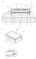
図6は、SOI構造のウェーハを用いて形成された光配線構造を示す概略断面図である。 FIG. 6 is a schematic sectional view showing an optical wiring structure formed using a wafer having an SOI structure.
図6に示すように、SOI構造のウェーハを用いた従来例による光配線構造では、第1シリコン層50と、酸化シリコン層(SiO2層)51と、第2シリコン層52とがこの順に積層されてSOI構造のウェーハを構成し、かつ酸化シリコン層51と第1シリコン層50との間に、光導波層(例えばゲルマニウムドープのシリコン層)53が挟持されいる。また、第2シリコン層52上にはバイポーラトランジスタ、MOSトランジスタ等の半導体集積回路54が組み込まれている。そして、SOI構造のウェーハはプリント配線基板62上に配置される。また、プリント配線基板62上には、レーザー等の発光素子55が、光導波層53の光入射端面56に対応した位置に配置されており、さらに、光導波層53の光出射端面57はミラー面に形成されており、この光出射端面57の中心線の直上にフォトダイオード等の受光素子58が配置されている。 As shown in FIG. 6, in the conventional optical wiring structure using the SOI structure wafer, the first silicon layer 50, the silicon oxide layer (SiO 2 layer) 51, and the second silicon layer 52 are laminated in this order. Thus, an SOI structure wafer is formed, and an optical waveguide layer (eg, germanium-doped silicon layer) 53 is sandwiched between the silicon oxide layer 51 and the first silicon layer 50. A semiconductor integrated circuit 54 such as a bipolar transistor or a MOS transistor is incorporated on the second silicon layer 52. The SOI structure wafer is disposed on the printed wiring board 62. On the printed circuit board 62, a light emitting element 55 such as a laser is disposed at a position corresponding to the light incident end face 56 of the optical waveguide layer 53, and the light emitting end face 57 of the optical waveguide layer 53 is a mirror. The light receiving element 58 such as a photodiode is disposed immediately above the center line of the light emitting end face 57.
この光配線構造の光伝搬メカニズムは、発光素子55から出射された光信号59aをレンズ等の光学部品60で集光し、光導波層53へ導入する。光導波層53へ導入された光信号59bは、光導波層53を導波し、ミラー面の光出射端面57にて垂直方向に偏光され、貫通孔61を通って出射される。出射光59cは、レンズ等の光学部品60によって集光され、光導波層53の光出射端面57の中心線の直上に配置された受光素子58に受光される。 The light propagation mechanism of this optical wiring structure condenses the optical signal 59 a emitted from the light emitting element 55 by the optical component 60 such as a lens and introduces it to the optical waveguide layer 53. The optical signal 59 b introduced into the optical waveguide layer 53 is guided through the optical waveguide layer 53, is polarized in the vertical direction at the light exit end face 57 of the mirror surface, and is emitted through the through hole 61. The emitted light 59c is collected by an optical component 60 such as a lens and received by the light receiving element 58 disposed immediately above the center line of the light emitting end face 57 of the optical waveguide layer 53.
このようなSOI構造のウェーハによる光配線構造を用いることにより、デジタル回路での高速及び低消費電力動作が可能となり、高周波回路での動作周波数の向上及びノイズの低減を図ることができ、ラッチアップの完全抑制やソフトエラー発生率の低減を実現することができる。 By using such an optical wiring structure with a wafer having an SOI structure, high-speed and low-power consumption operation is possible in a digital circuit, and the operating frequency in a high-frequency circuit can be improved and noise can be reduced. Can be completely suppressed and the occurrence rate of soft errors can be reduced.
上記したSOI構造のウェーハを用いた従来例による光配線構造では、SOI構造のウェーハ、受光素子及び発光素子をそれぞれ、光軸合わせしてプリント配線基板上に搭載し、更にレンズ等の光学部品による集光を行っている。しかしながら、プリント配線基板やこのプリント配線基板上に実装したその他の部品の熱変形、及び外力による変形により、光軸がずれてしまい、光結合ロスが大きい。 In the conventional optical wiring structure using the SOI structure wafer described above, the SOI structure wafer, the light receiving element, and the light emitting element are mounted on the printed wiring board with their optical axes aligned, and further by optical components such as lenses. Condensing light. However, the optical axis shifts due to thermal deformation of the printed wiring board and other components mounted on the printed wiring board and deformation due to external force, resulting in a large optical coupling loss.
本発明は、上述したような問題点を解決するためになされたものであって、その目的は、光結合ロスを低減することができる光導波モジュール及びその実装構造を提供することにある。 The present invention has been made to solve the above-described problems, and an object thereof is to provide an optical waveguide module capable of reducing optical coupling loss and a mounting structure thereof.
即ち、本発明は、第1の半導体層、絶縁層及び第2の半導体層とがこの順に積層され、前記第1の半導体層と前記第2の半導体層との間に光導波層が形成されている光導波装置と、光電変換素子とが、インターポーザー(例えばセラミクス製)に配されている、光導波モジュールに係るものである。 That is, according to the present invention, a first semiconductor layer, an insulating layer, and a second semiconductor layer are stacked in this order, and an optical waveguide layer is formed between the first semiconductor layer and the second semiconductor layer. The optical waveguide device and the photoelectric conversion element are related to an optical waveguide module arranged in an interposer (for example, made by Ceramics).
また、本発明の光導波モジュールが、前記インターポーザーを介して実装基板に実装されている、光導波モジュールの実装構造に係るものである。 Moreover, the optical waveguide module of the present invention relates to a mounting structure for an optical waveguide module, which is mounted on a mounting substrate via the interposer.
本発明によれば、前記光導波装置と、前記光電変換素子とが、セラミクス等の前記インターポーザーに配されているので、前記実装基板やこの実装基板上に実装したその他の部品が熱変形したり、外力によって変形しても、前記実装基板と比べて剛性が高くて変形し難い前記インターポーザーを介することによって光軸がずれ難く、光結合効率を飛躍的に改善することができ、生産性に優れている。 According to the present invention, since the optical waveguide device and the photoelectric conversion element are disposed in the interposer such as ceramics, the mounting substrate and other components mounted on the mounting substrate are thermally deformed. Even when deformed by external force, the optical axis is difficult to shift through the interposer, which has higher rigidity than the mounting substrate and is not easily deformed, and the optical coupling efficiency can be drastically improved. Is excellent.
また、光結合ロスを低減することができるので、前記光電変換素子の出力を抑えて低消費電力化が可能となる。 In addition, since the optical coupling loss can be reduced, it is possible to reduce the power consumption by suppressing the output of the photoelectric conversion element.
また、前記インターポーザーを用いることによって設計の自由度が向上し、その結果、商品開発のスピードの向上、部品の共通化による低コスト化が可能である。 In addition, the use of the interposer increases the degree of freedom in design, and as a result, the speed of product development can be improved and the cost can be reduced by sharing parts.
さらに、前記インターポーザーを用いることによってアライメントが容易となり、アライメントにかかるコストを低減させることができるため、低価格なシステムの提供が可能となる。 Furthermore, alignment can be facilitated by using the interposer, and the cost for alignment can be reduced, so that a low-cost system can be provided.
本発明の光導波モジュールは上述したような優れた効果を奏するので、光通信等の光情報処理装置として好適に機能することができる。 Since the optical waveguide module of the present invention has the excellent effects as described above, it can function suitably as an optical information processing apparatus such as optical communication.
本発明の光導波モジュールにおいて、前記光電変換素子が、前記光導波装置の前記光導波層に光を入射させる光入射手段(例えば、半導体レーザー等の発光素子)と、前記光導波層からの出射光を受光する受光手段(例えば、受光素子(光配線やフォトダイオード等)等)とのうちの少なくとも前記光入射手段であることが望ましい。 In the optical waveguide module of the present invention, the photoelectric conversion element includes a light incident means (for example, a light emitting element such as a semiconductor laser) that makes light incident on the optical waveguide layer of the optical waveguide device, and an output from the optical waveguide layer. It is desirable that the light incident means is at least one of light receiving means (for example, a light receiving element (such as an optical wiring or a photodiode)) that receives incident light.
また、前記光導波層の屈折率が、前記第1の半導体層及び前記絶縁層の屈折率より高いことが望ましく、これにより前記光導波層にて効果的な光信号の導波を行うことができる。 In addition, it is desirable that the refractive index of the optical waveguide layer is higher than the refractive indexes of the first semiconductor layer and the insulating layer, so that an effective optical signal can be guided in the optical waveguide layer. it can.
具体的には、前記第1の半導体層としてのシリコン基体に不純物元素のドープによって前記光導波層が形成されていることが好ましい。また、前記不純物元素はシリコンよりも屈折率の高い元素であれば良く、例えばゲルマニウムからなるのが好ましい。 Specifically, it is preferable that the optical waveguide layer is formed by doping an impurity element on a silicon substrate as the first semiconductor layer. The impurity element may be an element having a refractive index higher than that of silicon, and is preferably made of germanium, for example.
また、前記シリコン基体に前記光導波層としてのゲルマニウムドープのシリコン層が形成され、更にこのゲルマニウムドープのシリコン層上に、前記絶縁層としての酸化シリコン層及び前記第2の半導体層としてのシリコン層が設けられていることが望ましい。 Further, a germanium-doped silicon layer as the optical waveguide layer is formed on the silicon substrate, and a silicon oxide layer as the insulating layer and a silicon layer as the second semiconductor layer are further formed on the germanium-doped silicon layer. It is desirable to be provided.
そして、前記第2の半導体層に集積回路が形成されていることが好ましい。また、前記集積回路が、前記光電変換素子の駆動回路を有するのが好ましい。 An integrated circuit is preferably formed in the second semiconductor layer. The integrated circuit preferably includes a driving circuit for the photoelectric conversion element.
また、前記光電変換素子がサブマウント基板に配置され、このサブマウント基板を介して前記光電変換素子が前記インターポーザーに配されていることが好ましい。一般に前記光電変換素子の材料としてはGaAsなどを使用するが、これは取り扱いがデリケートであり、実装の際におけるハンドリング方法によってはチップ欠けなどを生じて不良としてしまうことがある。これに対し、本発明に基づく光導波モジュールによれば、前記サブマウント基板を介して前記光電変換素子が前記インターポーザーに配されるので、ハンドリングによるチップ欠け不良を効果的に低減することができる。 The photoelectric conversion element is preferably disposed on a submount substrate, and the photoelectric conversion element is disposed on the interposer via the submount substrate. Generally, GaAs or the like is used as the material of the photoelectric conversion element. However, this is delicate handling, and chipping or the like may occur depending on the handling method at the time of mounting, which may be defective. On the other hand, according to the optical waveguide module according to the present invention, since the photoelectric conversion element is arranged on the interposer via the submount substrate, chip chip defects due to handling can be effectively reduced. .
また、シリコン等からなる前記サブマウント基板を用いることにより、放熱効果による温度特性の向上を図ることができる。 Further, by using the submount substrate made of silicon or the like, it is possible to improve temperature characteristics due to a heat dissipation effect.
また、前記サブマウント基板にアライメントマーク等を設けることが好ましい。これにより、前記光電変換素子を前記サブマウント基板に実装するときに、前記アライメントマークを基準に光軸を容易に調整することができる。また、前記サブマウント基板を介して前記光電変換素子を前記インターポーザーに配するときに、前記アライメントマークを使用することで、アセンブリが一層容易になる。 Moreover, it is preferable to provide an alignment mark or the like on the submount substrate. Accordingly, when the photoelectric conversion element is mounted on the submount substrate, the optical axis can be easily adjusted based on the alignment mark. In addition, when the photoelectric conversion element is arranged on the interposer via the submount substrate, the assembly is further facilitated by using the alignment mark.
さらに、前記サブマウント基板上に、前記光電変換素子としての発光素子の出力をモニタできるフォトディテクタが配置されているのが好ましい。例えば、前記サブマウント基板としてのシリコン基体に不純物元素のドープによって前記フォトディテクタを形成することができる。前記サブマウント基板に前記フォトディテクタを設けることにより、半導体レーザー等の前記発光素子の出力をモニタできるので、前記発光素子のAPC(オートパワーコントロール)が可能となる。 Furthermore, it is preferable that a photodetector capable of monitoring the output of the light emitting element as the photoelectric conversion element is disposed on the submount substrate. For example, the photodetector can be formed by doping an impurity element on a silicon substrate as the submount substrate. By providing the photodetector on the submount substrate, the output of the light emitting element such as a semiconductor laser can be monitored, so that APC (auto power control) of the light emitting element becomes possible.
本発明の光導波モジュールの実装構造において、前記光電変換素子としての前記受光手段は前記インターポーザー上に配されていることが好ましく、或いは、前記実装基板上に配されていることが好ましい。前記受光手段が前記実装基板上に配されている場合、前記光導波層の光出射端面で導波光が反射されて、前記受光手段へ光路変換されるのが好ましい。 In the optical waveguide module mounting structure of the present invention, the light receiving means as the photoelectric conversion element is preferably disposed on the interposer, or is preferably disposed on the mounting substrate. When the light receiving means is disposed on the mounting substrate, it is preferable that the guided light is reflected by the light emitting end face of the optical waveguide layer and the optical path is changed to the light receiving means.
上記のように、本発明に基づく光導波モジュール及びその実装構造はSOI(Silicon On Insulator)構造によるウェーハを用いるので、デジタル回路での高速及び低消費電力動作が可能となり、高周波回路での動作周波数の向上及びノイズの低減を図ることができ、ラッチアップの完全抑制やソフトエラー発生率の低減を実現することができる。 As described above, the optical waveguide module and the mounting structure thereof according to the present invention use a wafer having an SOI (Silicon On Insulator) structure, so that high-speed and low-power consumption operation in a digital circuit is possible, and an operation frequency in a high-frequency circuit. Can be improved and noise can be reduced, and latch-up can be completely suppressed and the soft error rate can be reduced.
そして、上述したようなSOI構造によるウェーハを用いたことによる効果と共に、前記光導波装置と、前記光電変換素子とが、前記インターポーザーに配されているので、前記実装基板やこの実装基板上に実装したその他の部品が熱変形したり、外力によって変形しても、前記実装基板と比べて高剛性でありかつ信頼性の高い前記インターポーザーを介することによって光軸がずれ難く、光結合効率を飛躍的に改善することができ、生産性に優れている。 And with the effect by having used the wafer by SOI structure as mentioned above, since the said optical waveguide device and the said photoelectric conversion element are distribute | arranged to the said interposer, on the said mounting substrate or this mounting substrate Even if other mounted components are thermally deformed or deformed by an external force, the optical axis is difficult to shift through the interposer having high rigidity and high reliability compared to the mounting substrate, and the optical coupling efficiency is improved. It can dramatically improve and is highly productive.
また、光結合ロスを低減することができるので、前記光電変換素子の出力を抑えて低消費電力化が可能となる。 In addition, since the optical coupling loss can be reduced, it is possible to reduce the power consumption by suppressing the output of the photoelectric conversion element.
また、前記インターポーザーを用いることによって設計の自由度が向上し、その結果、商品開発のスピードの向上、部品の共通化による低コスト化が可能である。 In addition, the use of the interposer increases the degree of freedom in design, and as a result, the speed of product development can be improved and the cost can be reduced by sharing parts.
さらに、前記インターポーザーを用いることによってアライメントが容易となり、アライメントにかかるコストを低減させることができるため、低価格なシステムの提供が可能となる。 Furthermore, alignment can be facilitated by using the interposer, and the cost for alignment can be reduced, so that a low-cost system can be provided.
本発明は、前記受光手段を前記光導波層に位置合わせして配置することにより、前記光導波層に効率良く入射した光信号を次段回路の前記受光手段に入射させるように構成した光通信等の光情報処理に有効に用いることができる。 According to the present invention, an optical communication configured such that an optical signal efficiently incident on the optical waveguide layer is incident on the light receiving unit of the next stage circuit by arranging the light receiving unit in alignment with the optical waveguide layer. It can be effectively used for optical information processing.
以下、本発明の好ましい実施の形態を図面を参照して説明する。 Hereinafter, preferred embodiments of the present invention will be described with reference to the drawings.
第1の実施の形態
図1は、本発明に基づく光導波モジュール及びその実装構造の概略図である。
First Embodiment FIG. 1 is a schematic view of an optical waveguide module and its mounting structure according to the present invention.
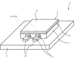
本実施の形態による光導波モジュール1は、図1(a)に示すように、光導波装置2と、前記光電変換素子としての光入射手段(例えば、半導体レーザー等の発光素子)3と、前記光電変換素子としての受光手段(例えば、フォトダイオード等の受光素子、又は光ファイバー)4とが、セラミクス等のインターポーザー5に配されている。また、本発明に基づく光導波モジュール1が、インターポーザー5を介して実装基板(プリント配線基板)6に実装されている。
As shown in FIG. 1A, an
光導波装置2は、図1(a)及び(b)に示すように、第1の半導体層7、絶縁層8及び第2の半導体層9とがこの順に積層され、第1の半導体層7と第2の半導体層9との間に光導波層10が形成されている。
As shown in FIGS. 1A and 1B, the optical waveguide device 2 includes a
また、光導波層10の屈折率が、第1の半導体層7及び絶縁層8の屈折率より高いことが望ましく、これにより光導波層10にて効果的な光信号11の導波を行うことができる。
In addition, it is desirable that the refractive index of the
具体的には、第1の半導体層7としてのシリコン基体に不純物元素のドープによって光導波層10が形成されていることが好ましい。また、前記不純物元素はシリコンよりも屈折率の高い元素であればよく、例えばゲルマニウムからなるのが好ましい。
Specifically, the
また、シリコン基体7に光導波層10としてのゲルマニウムドープのシリコン層が形成され、更にこのゲルマニウムドープのシリコン層10上に、絶縁層8としての酸化シリコン層(SiO2層)及び第2の半導体層9としてのシリコン層が設けられていることが望ましい。
Further, a germanium-doped silicon layer as the
そして、第2の半導体層9に集積回路12が形成されていることが好ましい(但し、図1(b)では前記集積回路は図示省略した。)。また、集積回路12が、光導波層10への光入射手段3及び光導波層10からの出射光の受光手段4の駆動回路(バイポーラトランジスタ、MOSトランジスタ等)を有するのが好ましい。
An
本発明に基づく光導波モジュール1において、ゲルマニウムドープのシリコン層10は、シリコン基体7や酸化シリコン層8よりも屈折率nが高いため、光信号11の導波路として効果的に機能する。ゲルマニウムドープのシリコン層10を通る波長としては970nm以上の近赤外波長域の光であり、一般に1.3μmや1.5μm近傍の波長のレーザーが光源として使われる。
In the
光入射手段3としての発光素子は、例えば図1(c)に示すように、GaAs等からなるクラッド層13a、13bと、これらクラッド層13a、13bに挟持された活性層14とを有する。また、クラッド層13a上には電極15が設けられており、図示省略したがクラッド層13b上にも電極が設けられている。
For example, as shown in FIG. 1C, the light emitting element as the light incident means 3 includes
本発明に基づく光導波モジュール1の光伝搬メカニズムは、光入射手段(発光素子)3から出射された光信号11が、光導波層10としてのゲルマニウムドープのシリコン層へ光入射端面16から導入される。光導波層10へ導入された光信号11は、光導波層10を導波し、その光出射端面17から出射され、出射された光信号11は、受光手段(受光素子)4によって受光される。
The optical propagation mechanism of the
このように、本発明に基づく光導波モジュール1及びその実装構造はSOI(Silicon On Insulator)構造によるウェーハを用いるので、デジタル回路での高速及び低消費電力動作が可能となり、高周波回路での動作周波数の向上及びノイズの低減を図ることができ、ラッチアップの完全抑制やソフトエラー発生率の低減を実現することができる。
Thus, since the
そして、上述したようなSOI構造によるウェーハを用いたことによる効果と共に、光導波装置2と、光電変換素子3、4とが、セラミクス等のインターポーザー5に配されているので、実装基板6やこの実装基板6上に実装したその他の部品(図示省略)が熱変形したり、外力によって変形しても、実装基板6と比べて剛性の高いインターポーザー5を介することによって光軸がずれ難く、光結合効率を飛躍的に改善することができ、生産性に優れている。
Since the optical waveguide device 2 and the
また、光結合ロスを低減することができるので、光電変換素子3、4の出力を抑えて低消費電力化が可能となる。
In addition, since the optical coupling loss can be reduced, the output of the
また、インターポーザー5を用いることによって設計の自由度が向上し、その結果、商品開発のスピードの向上、部品の共通化による低コスト化が可能である。
Further, the use of the
さらに、インターポーザー5を用いることによってアライメントが容易となり、アライメントにかかるコストを低減させることができるため、低価格なシステムの提供が可能となる。
Furthermore, the use of the
第2の実施の形態
本実施の形態における光導波モジュールは、図2に示すように、前記光電変換素子としての光入射手段(例えば、半導体レーザー等の発光素子)3がシリコン等からなるサブマウント基板18に配置され、このサブマウント基板18を介して光入射手段3がインターポーザー5に配されている。なお、前記光電変換素子としての受光手段(例えば、フォトダイオード等の受光素子)4についても同様である。
Second Embodiment As shown in FIG. 2, the optical waveguide module according to the present embodiment is a submount in which light incident means (for example, a light emitting element such as a semiconductor laser) 3 as the photoelectric conversion element is made of silicon or the like. The light incident means 3 is disposed on the
一般に発光素子3、受光素子4の材料としてはGaAsなどを使用するが、これは取り扱いがデリケートであり、実装の際におけるハンドリング方法によってはチップ欠けなどを生じて不良としてしまうことがある。これに対し、本実施の形態によれば、サブマウント基板18を介して前記光電変換素子としての発光素子3、受光素子4がインターポーザー5に配されるので、ハンドリングによるチップ欠け不良を低減することができる。
In general, GaAs or the like is used as the material of the light emitting element 3 and the
また、シリコン等からなるサブマウント基板18を用いることにより、放熱効果による温度特性の向上を図ることができる。
Further, by using the
また、図2(b)に示すように、サブマウント基板18にアライメントマーク19等を設けてもよい。これにより、発光素子3、受光素子4を実装するときにアライメントマーク19を基準に光軸を調整することができ、また、サブマウント基板18を介して発光素子3、受光素子4をインターポーザー5に配するときにアライメントマーク19を使用することで、アセンブリが一層容易になる。
Further, as shown in FIG. 2B, an
さらに、図2(c)に示すように、発光素子3を実装したサブマウント基板18にフォトディテクタ(PD)20を設けることが好ましい。これにより、半導体レーザー等の発光素子3の出力をモニタできるので、発光素子3のAPC(オートパワーコントロール)が可能となる。この場合、サブマウント基板18としてのシリコン基体に不純物元素のドープによってフォトディテクタ20を形成することができる。
Further, as shown in FIG. 2C, it is preferable to provide a photodetector (PD) 20 on the
なお、本発明に基づく光導波モジュール1を構成する光導波装置2において、光導波層10の数、形状等は適宜選択可能である。例えば、図3に示すように、光導波装置2に複数の光導波層10を設け、前記発光素子等の光入射手段3を、光導波層10の光入射端面16にそれぞれ対応させ、サブマウント基板18を介してインターポーザー5上に配置してもよい。また、発光素子3は全て同じ種類(発光光の波長が同じ)であっても、或いは互いに異なる種類のものでもよい。図3では図示省略したが、上述したと同様にして第2の半導体層9には前記集積回路が組み込まれているのが好ましい。
In the optical waveguide device 2 constituting the
第3の実施の形態
図4に示すように、前記光入射手段としての前記発光素子としてECL(Extra Cavity Laser)21を用いてもよい。ECL21は、ハーフミラー22、レーザーを構成する増幅媒体23、MEMS(Micro Electro Mechanical Systems)可動ミラー24及び可動ミラー24に接合されたアクチュエータ25からなる。アクチュエータ25によって可動ミラー24の位置を動かすことによりレーザーのキャビティ長を変化させ、波長の異なるレーザー光(λ1、λ2)11を発生させることができる。これにより、光導波層10に複数の波長の光信号11を入射させることができ、例えばブロック毎に特定の波長のみを受光する受光素子4を設けることにより、LSI中の動作が必要なブロックだけにクロックを配信することができる。
Third Embodiment As shown in FIG. 4, an ECL (Extra Cavity Laser) 21 may be used as the light emitting element as the light incident means. The
第4の実施の形態
前記光電変換素子としての前記受光手段は、例えばフォトダイオード等の受光素子が挙げられる。この受光手段は、例えば図5に示すように、実装基板6上に配置してもよい。具体的には、光導波層10の光出射端面17を傾斜面、例えば45度ミラー面に形成し、第1の半導体層7及びインターポーザー5における光出射端面17の直下に位置する領域に貫通孔26を設け、かつ実装基板6に凹部27を設け、この凹部27内に受光手段4を配置する。これにより、光導波層10の光出射端面17で導波光11が反射されて、受光手段4へ光路変換される。
Fourth Embodiment The light receiving means as the photoelectric conversion element may be a light receiving element such as a photodiode. For example, as shown in FIG. 5, the light receiving means may be disposed on the mounting substrate 6. Specifically, the light emitting end face 17 of the
この場合も、光導波装置2及び光入射手段3はインターポーザー5に配されているので、実装基板6及びこの実装基板6上に実装された他の部品等の熱変形、又は外力による変形が起きても、光軸がずれ難く、光結合ロスの低減を図ることができる。
Also in this case, since the optical waveguide device 2 and the light incident means 3 are arranged in the
以上、本発明を実施の形態について説明したが、上述の例は、本発明の技術的思想に基づき種々に変形が可能である。 As mentioned above, although embodiment of this invention was described, the above-mentioned example can be variously modified based on the technical idea of this invention.
例えば、ゲルマニウムドープのシリコン層を前記光導波層とする例を述べてきたが、ゲルマニウムドープのシリコン層以外にも酸化シリコン(SiO2)などを前記光導波層として使用することも可能である。例えば、酸化シリコンは透過率が非常に優れており、850nmといった通信用のレーザーの中でも比較的安価に製造されている近赤外レーザー光を低損失で透過させることができる。そこで、酸化シリコンからなる前記光導波層を更に低屈折率の材料からなる層で挟んだ構造とすることにより、上述したゲルマニウムドープのシリコン層と同様にして、酸化シリコンを前記光導波層として効果的に機能させることが可能である。 For example, although an example in which a germanium-doped silicon layer is used as the optical waveguide layer has been described, silicon oxide (SiO 2 ) or the like can be used as the optical waveguide layer in addition to the germanium-doped silicon layer. For example, silicon oxide has a very high transmittance, and can transmit near-infrared laser light manufactured at a relatively low cost among communication lasers of 850 nm with low loss. Therefore, by using a structure in which the optical waveguide layer made of silicon oxide is further sandwiched between layers made of a material having a low refractive index, silicon oxide is effective as the optical waveguide layer in the same manner as the germanium-doped silicon layer described above. Can be functional.
また、前記光導波層へ前記光信号を導入するには、前記発光素子等の前記光入射手段から直接光信号を前記光導波層へ入射するバットカップリング法、一度レンズ等の光学部品で集光して光信号のビーム径を小さくしてから前記光導波層へ入射させるレンズカップリング法などで行うことができる。 In addition, in order to introduce the optical signal into the optical waveguide layer, the optical signal is directly incident on the optical waveguide layer from the light incident means such as the light emitting element, and once collected by an optical component such as a lens. This can be performed by a lens coupling method in which light is used to reduce the beam diameter of an optical signal and then enter the optical waveguide layer.
さらに、前記受光手段の配置位置は上述したように前記インターポーザー上であっても、或いは前記実装基板上であってもよいが、これらに特に限定されず、図6に示すような従来例のように、前記光導波層の前記光出射端面をミラー面に形成し、前記光導波層の光出射端面の中心線の直上に前記受光手段を配置してもよい。この場合、前記光導波層を導波した光信号は、前記光導波層のミラー面の前記光出射端面にて垂直方向に偏光され、貫通孔を通過して、前記光導波層の前記光出射端面の中心線の直上に配置された前記受光手段に受光される。 Further, the arrangement position of the light receiving means may be on the interposer as described above or on the mounting substrate, but is not particularly limited to this, and the conventional example as shown in FIG. As described above, the light emitting end face of the optical waveguide layer may be formed on a mirror surface, and the light receiving means may be disposed immediately above the center line of the light emitting end face of the optical waveguide layer. In this case, the optical signal guided through the optical waveguide layer is polarized in the vertical direction at the light output end face of the mirror surface of the optical waveguide layer, passes through a through-hole, and the light output from the optical waveguide layer. The light is received by the light receiving means arranged immediately above the center line of the end face.
1…光導波モジュール、2…光導波装置、3…光入射手段、4…受光手段、
5…インターポーザー、6…実装基板、7…第1の半導体層、8…絶縁層、
9…第2の半導体層、10…光導波層、11…光信号、12…集積回路、
13a、13b…クラッド層、14…活性層、15…電極、16…光入射端面、
17…光出射端面、18…サブマウント基板、19…アライメントマーク、
20…フォトディテクタ、21…ECL、22…ハーフミラー、23…増幅媒体、
24…可動ミラー、25…アクチュエータ、26…貫通孔、27…凹部
DESCRIPTION OF
5 ... Interposer, 6 ... Mounting substrate, 7 ... First semiconductor layer, 8 ... Insulating layer,
DESCRIPTION OF
13a, 13b ... cladding layer, 14 ... active layer, 15 ... electrode, 16 ... light incident end face,
17 ... Light emitting end face, 18 ... Submount substrate, 19 ... Alignment mark,
20 ... Photo detector, 21 ... ECL, 22 ... Half mirror, 23 ... Amplification medium,
24 ...
Claims (15)
Priority Applications (1)
| Application Number | Priority Date | Filing Date | Title |
|---|---|---|---|
| JP2004236536A JP2006053473A (en) | 2004-08-16 | 2004-08-16 | Optical waveguide module and mounting structure thereof |
Applications Claiming Priority (1)
| Application Number | Priority Date | Filing Date | Title |
|---|---|---|---|
| JP2004236536A JP2006053473A (en) | 2004-08-16 | 2004-08-16 | Optical waveguide module and mounting structure thereof |
Publications (1)
| Publication Number | Publication Date |
|---|---|
| JP2006053473A true JP2006053473A (en) | 2006-02-23 |
Family
ID=36030973
Family Applications (1)
| Application Number | Title | Priority Date | Filing Date |
|---|---|---|---|
| JP2004236536A Pending JP2006053473A (en) | 2004-08-16 | 2004-08-16 | Optical waveguide module and mounting structure thereof |
Country Status (1)
| Country | Link |
|---|---|
| JP (1) | JP2006053473A (en) |
Cited By (4)
| Publication number | Priority date | Publication date | Assignee | Title |
|---|---|---|---|---|
| US8705906B2 (en) | 2009-04-23 | 2014-04-22 | Korea Electronics Technology Institute | Photoelectric conversion module |
| JP2018194648A (en) * | 2017-05-16 | 2018-12-06 | 富士通オプティカルコンポーネンツ株式会社 | Optical transmitter and optical receiver |
| JP2019207976A (en) * | 2018-05-30 | 2019-12-05 | 日亜化学工業株式会社 | Light source device |
| CN117250702A (en) * | 2023-11-20 | 2023-12-19 | 之江实验室 | Photoelectric co-packaging module and photoelectric co-packaging method |
Citations (10)
| Publication number | Priority date | Publication date | Assignee | Title |
|---|---|---|---|---|
| JPS6188588A (en) * | 1984-10-08 | 1986-05-06 | Sony Corp | Manufacture of semiconductor laser |
| JPS6190488A (en) * | 1984-10-09 | 1986-05-08 | Sony Corp | Semiconductor device and manufacture thereof |
| JPS6195591A (en) * | 1984-10-16 | 1986-05-14 | Sony Corp | Semiconductor laser |
| JPH11202159A (en) * | 1998-01-19 | 1999-07-30 | Oki Electric Ind Co Ltd | Manufacture of optical circuit module |
| JP2000047055A (en) * | 1998-07-28 | 2000-02-18 | Japan Aviation Electronics Industry Ltd | Optical waveguide device and its production |
| JP2001183556A (en) * | 1999-12-27 | 2001-07-06 | Toppan Printing Co Ltd | Multi-chip module board and multi-chip module |
| JP2003222746A (en) * | 2002-01-29 | 2003-08-08 | Mitsubishi Electric Corp | Photoelectric coupling device |
| JP2003322741A (en) * | 2002-05-08 | 2003-11-14 | Mitsubishi Electric Corp | Optical and electronic parts mixedly loaded substrate |
| EP1378777A2 (en) * | 2002-07-02 | 2004-01-07 | Omron Corporation | Optical waveguide device, manufacturing method thereof, and optical communication apparatus |
| WO2004010192A2 (en) * | 2002-07-22 | 2004-01-29 | Applied Materials Inc. | Optical-ready substrates with optical waveguide circuits and microelectronic circuits |
-
2004
- 2004-08-16 JP JP2004236536A patent/JP2006053473A/en active Pending
Patent Citations (10)
| Publication number | Priority date | Publication date | Assignee | Title |
|---|---|---|---|---|
| JPS6188588A (en) * | 1984-10-08 | 1986-05-06 | Sony Corp | Manufacture of semiconductor laser |
| JPS6190488A (en) * | 1984-10-09 | 1986-05-08 | Sony Corp | Semiconductor device and manufacture thereof |
| JPS6195591A (en) * | 1984-10-16 | 1986-05-14 | Sony Corp | Semiconductor laser |
| JPH11202159A (en) * | 1998-01-19 | 1999-07-30 | Oki Electric Ind Co Ltd | Manufacture of optical circuit module |
| JP2000047055A (en) * | 1998-07-28 | 2000-02-18 | Japan Aviation Electronics Industry Ltd | Optical waveguide device and its production |
| JP2001183556A (en) * | 1999-12-27 | 2001-07-06 | Toppan Printing Co Ltd | Multi-chip module board and multi-chip module |
| JP2003222746A (en) * | 2002-01-29 | 2003-08-08 | Mitsubishi Electric Corp | Photoelectric coupling device |
| JP2003322741A (en) * | 2002-05-08 | 2003-11-14 | Mitsubishi Electric Corp | Optical and electronic parts mixedly loaded substrate |
| EP1378777A2 (en) * | 2002-07-02 | 2004-01-07 | Omron Corporation | Optical waveguide device, manufacturing method thereof, and optical communication apparatus |
| WO2004010192A2 (en) * | 2002-07-22 | 2004-01-29 | Applied Materials Inc. | Optical-ready substrates with optical waveguide circuits and microelectronic circuits |
Cited By (6)
| Publication number | Priority date | Publication date | Assignee | Title |
|---|---|---|---|---|
| US8705906B2 (en) | 2009-04-23 | 2014-04-22 | Korea Electronics Technology Institute | Photoelectric conversion module |
| JP2018194648A (en) * | 2017-05-16 | 2018-12-06 | 富士通オプティカルコンポーネンツ株式会社 | Optical transmitter and optical receiver |
| JP2019207976A (en) * | 2018-05-30 | 2019-12-05 | 日亜化学工業株式会社 | Light source device |
| JP7060798B2 (en) | 2018-05-30 | 2022-04-27 | 日亜化学工業株式会社 | Light source device |
| CN117250702A (en) * | 2023-11-20 | 2023-12-19 | 之江实验室 | Photoelectric co-packaging module and photoelectric co-packaging method |
| CN117250702B (en) * | 2023-11-20 | 2024-02-23 | 之江实验室 | Photoelectric co-packaging module and photoelectric co-packaging method |
Similar Documents
| Publication | Publication Date | Title |
|---|---|---|
| US10168474B2 (en) | Method of manufacturing optical input/output device | |
| CN107040318B (en) | Method and system for communication | |
| TWI522668B (en) | Optical waveguide and optical waveguide module | |
| US9331096B2 (en) | Method and system for hybrid integration of optical communication systems | |
| US9329349B2 (en) | Integrated optical cooling core for optoelectronic interconnect modules | |
| US7366375B2 (en) | Optical waveguide device, manufacturing method thereof, optical information processing apparatus, and electronic equipment | |
| JP5439080B2 (en) | Optical I / O array module | |
| Ciftcioglu et al. | 3-D integrated heterogeneous intra-chip free-space optical interconnect | |
| EP2696229A2 (en) | Method and system for hybrid integration of optical communication systems | |
| US7876984B2 (en) | Planar optical waveguide array module and method of fabricating the same | |
| JP4412105B2 (en) | Optical waveguide device | |
| JP4292476B2 (en) | Optical waveguide module and optical information processing apparatus | |
| US10365431B2 (en) | Optical interconnect structure | |
| US20060024067A1 (en) | Optical I/O chip for use with distinct electronic chip | |
| JP2006053473A (en) | Optical waveguide module and mounting structure thereof | |
| JP2013012548A (en) | Optical module and photo-electric hybrid board | |
| JP2007019133A (en) | Photoelectric conversion device, its manufacturing method, and optical information process device | |
| JP4654801B2 (en) | PHOTOELECTRIC CONVERSION DEVICE, ITS MANUFACTURING METHOD, AND OPTICAL INFORMATION PROCESSING DEVICE | |
| JP4543956B2 (en) | Semiconductor device and electronic apparatus using the same | |
| JP5898732B2 (en) | Manufacturing method of optical module | |
| JP2006195197A (en) | Manufacturing method of optical waveguide and die used in manufacturing the same | |
| JP2006310417A (en) | Photoelectric converter, its manufacturing method and optical information processor | |
| JP2006053471A (en) | Optical waveguide device, fabrication method thereof and optical information processing apparatus | |
| WO2023084610A1 (en) | Optical module and creation method for same | |
| Liu et al. | Polymer waveguide applications in multichip modules (MCMs) and board level optical interconnects |
Legal Events
| Date | Code | Title | Description |
|---|---|---|---|
| RD13 | Notification of appointment of power of sub attorney |
Free format text: JAPANESE INTERMEDIATE CODE: A7433 Effective date: 20070125 |
|
| A621 | Written request for application examination |
Free format text: JAPANESE INTERMEDIATE CODE: A621 Effective date: 20070426 |
|
| A977 | Report on retrieval |
Free format text: JAPANESE INTERMEDIATE CODE: A971007 Effective date: 20090406 |
|
| A131 | Notification of reasons for refusal |
Free format text: JAPANESE INTERMEDIATE CODE: A131 Effective date: 20090414 |
|
| A521 | Request for written amendment filed |
Free format text: JAPANESE INTERMEDIATE CODE: A523 Effective date: 20090521 |
|
| RD02 | Notification of acceptance of power of attorney |
Free format text: JAPANESE INTERMEDIATE CODE: A7422 Effective date: 20090527 |
|
| A02 | Decision of refusal |
Free format text: JAPANESE INTERMEDIATE CODE: A02 Effective date: 20100323 |