JP2005531158A - Semiconductor device and semiconductor device manufacturing method - Google Patents
Semiconductor device and semiconductor device manufacturing method Download PDFInfo
- Publication number
- JP2005531158A JP2005531158A JP2004517659A JP2004517659A JP2005531158A JP 2005531158 A JP2005531158 A JP 2005531158A JP 2004517659 A JP2004517659 A JP 2004517659A JP 2004517659 A JP2004517659 A JP 2004517659A JP 2005531158 A JP2005531158 A JP 2005531158A
- Authority
- JP
- Japan
- Prior art keywords
- gate electrode
- doping
- layer
- gate
- electrode layer
- Prior art date
- Legal status (The legal status is an assumption and is not a legal conclusion. Google has not performed a legal analysis and makes no representation as to the accuracy of the status listed.)
- Pending
Links
- 239000004065 semiconductor Substances 0.000 title claims abstract description 57
- 238000004519 manufacturing process Methods 0.000 title abstract description 12
- 238000000034 method Methods 0.000 claims abstract description 178
- 238000000151 deposition Methods 0.000 claims abstract description 70
- 239000002019 doping agent Substances 0.000 claims abstract description 63
- 238000002513 implantation Methods 0.000 claims abstract description 61
- ZOXJGFHDIHLPTG-UHFFFAOYSA-N Boron Chemical compound [B] ZOXJGFHDIHLPTG-UHFFFAOYSA-N 0.000 claims abstract description 59
- 229910052796 boron Inorganic materials 0.000 claims abstract description 59
- 239000000758 substrate Substances 0.000 claims abstract description 50
- 230000008021 deposition Effects 0.000 claims abstract description 44
- 238000005468 ion implantation Methods 0.000 claims abstract description 30
- 239000001257 hydrogen Substances 0.000 claims abstract description 27
- 229910052739 hydrogen Inorganic materials 0.000 claims abstract description 27
- 238000000059 patterning Methods 0.000 claims abstract description 17
- 230000008569 process Effects 0.000 claims description 116
- UFHFLCQGNIYNRP-UHFFFAOYSA-N Hydrogen Chemical compound [H][H] UFHFLCQGNIYNRP-UHFFFAOYSA-N 0.000 claims description 23
- 238000010438 heat treatment Methods 0.000 claims description 23
- 229920002120 photoresistant polymer Polymers 0.000 claims description 23
- VYPSYNLAJGMNEJ-UHFFFAOYSA-N Silicium dioxide Chemical compound O=[Si]=O VYPSYNLAJGMNEJ-UHFFFAOYSA-N 0.000 claims description 20
- 239000000463 material Substances 0.000 claims description 15
- 229910021420 polycrystalline silicon Inorganic materials 0.000 claims description 14
- 229920005591 polysilicon Polymers 0.000 claims description 13
- 229910052710 silicon Inorganic materials 0.000 claims description 13
- 239000010703 silicon Substances 0.000 claims description 13
- 235000012239 silicon dioxide Nutrition 0.000 claims description 10
- 239000000377 silicon dioxide Substances 0.000 claims description 10
- 239000003989 dielectric material Substances 0.000 claims description 9
- 125000006850 spacer group Chemical group 0.000 claims description 8
- 229910021417 amorphous silicon Inorganic materials 0.000 claims description 7
- 150000002500 ions Chemical class 0.000 claims description 7
- 238000002955 isolation Methods 0.000 claims description 7
- 229910044991 metal oxide Inorganic materials 0.000 claims description 6
- 150000004706 metal oxides Chemical class 0.000 claims description 6
- 150000001638 boron Chemical class 0.000 claims description 5
- 230000008929 regeneration Effects 0.000 claims description 2
- 238000011069 regeneration method Methods 0.000 claims description 2
- 239000000126 substance Substances 0.000 claims description 2
- 239000007943 implant Substances 0.000 abstract description 47
- 230000008901 benefit Effects 0.000 abstract description 8
- 238000005137 deposition process Methods 0.000 abstract description 5
- 125000004435 hydrogen atom Chemical class [H]* 0.000 abstract 1
- 230000000149 penetrating effect Effects 0.000 abstract 1
- 239000010410 layer Substances 0.000 description 100
- 230000015572 biosynthetic process Effects 0.000 description 38
- 238000009792 diffusion process Methods 0.000 description 35
- 238000000137 annealing Methods 0.000 description 23
- 230000035515 penetration Effects 0.000 description 19
- 238000010586 diagram Methods 0.000 description 16
- XUIMIQQOPSSXEZ-UHFFFAOYSA-N Silicon Chemical compound [Si] XUIMIQQOPSSXEZ-UHFFFAOYSA-N 0.000 description 12
- 230000007547 defect Effects 0.000 description 10
- 238000002347 injection Methods 0.000 description 9
- 239000007924 injection Substances 0.000 description 9
- 238000010884 ion-beam technique Methods 0.000 description 9
- IJGRMHOSHXDMSA-UHFFFAOYSA-N Atomic nitrogen Chemical compound N#N IJGRMHOSHXDMSA-UHFFFAOYSA-N 0.000 description 8
- 238000011109 contamination Methods 0.000 description 8
- 230000000694 effects Effects 0.000 description 8
- 238000005516 engineering process Methods 0.000 description 8
- 238000012545 processing Methods 0.000 description 8
- 230000007261 regionalization Effects 0.000 description 7
- 125000004429 atom Chemical group 0.000 description 6
- 238000007796 conventional method Methods 0.000 description 6
- 230000002829 reductive effect Effects 0.000 description 5
- 230000009286 beneficial effect Effects 0.000 description 4
- 239000007772 electrode material Substances 0.000 description 4
- 229910052751 metal Inorganic materials 0.000 description 4
- 239000002184 metal Substances 0.000 description 4
- 229910052757 nitrogen Inorganic materials 0.000 description 4
- 239000007787 solid Substances 0.000 description 4
- 229910000577 Silicon-germanium Inorganic materials 0.000 description 3
- 238000013459 approach Methods 0.000 description 3
- 150000002431 hydrogen Chemical class 0.000 description 3
- 230000001976 improved effect Effects 0.000 description 3
- 238000001465 metallisation Methods 0.000 description 3
- 238000005457 optimization Methods 0.000 description 3
- QGZKDVFQNNGYKY-UHFFFAOYSA-N Ammonia Chemical compound N QGZKDVFQNNGYKY-UHFFFAOYSA-N 0.000 description 2
- 229910052581 Si3N4 Inorganic materials 0.000 description 2
- 230000007423 decrease Effects 0.000 description 2
- 230000001627 detrimental effect Effects 0.000 description 2
- 239000000203 mixture Substances 0.000 description 2
- 238000012986 modification Methods 0.000 description 2
- 230000004048 modification Effects 0.000 description 2
- HQVNEWCFYHHQES-UHFFFAOYSA-N silicon nitride Chemical compound N12[Si]34N5[Si]62N3[Si]51N64 HQVNEWCFYHHQES-UHFFFAOYSA-N 0.000 description 2
- 239000000243 solution Substances 0.000 description 2
- BPQQTUXANYXVAA-UHFFFAOYSA-N Orthosilicate Chemical compound [O-][Si]([O-])([O-])[O-] BPQQTUXANYXVAA-UHFFFAOYSA-N 0.000 description 1
- 230000001133 acceleration Effects 0.000 description 1
- 230000009471 action Effects 0.000 description 1
- 230000002411 adverse Effects 0.000 description 1
- 230000004075 alteration Effects 0.000 description 1
- 229910021529 ammonia Inorganic materials 0.000 description 1
- 238000004458 analytical method Methods 0.000 description 1
- 229910052785 arsenic Inorganic materials 0.000 description 1
- RQNWIZPPADIBDY-UHFFFAOYSA-N arsenic atom Chemical compound [As] RQNWIZPPADIBDY-UHFFFAOYSA-N 0.000 description 1
- HAYXDMNJJFVXCI-UHFFFAOYSA-N arsenic(5+) Chemical compound [As+5] HAYXDMNJJFVXCI-UHFFFAOYSA-N 0.000 description 1
- UORVGPXVDQYIDP-UHFFFAOYSA-N borane Chemical class B UORVGPXVDQYIDP-UHFFFAOYSA-N 0.000 description 1
- 230000015556 catabolic process Effects 0.000 description 1
- 230000005465 channeling Effects 0.000 description 1
- 230000000295 complement effect Effects 0.000 description 1
- 239000002131 composite material Substances 0.000 description 1
- 230000001010 compromised effect Effects 0.000 description 1
- 239000013078 crystal Substances 0.000 description 1
- 238000006731 degradation reaction Methods 0.000 description 1
- 230000000593 degrading effect Effects 0.000 description 1
- 238000011161 development Methods 0.000 description 1
- 230000018109 developmental process Effects 0.000 description 1
- 239000006185 dispersion Substances 0.000 description 1
- 230000005684 electric field Effects 0.000 description 1
- 238000000605 extraction Methods 0.000 description 1
- 229910052735 hafnium Inorganic materials 0.000 description 1
- VBJZVLUMGGDVMO-UHFFFAOYSA-N hafnium atom Chemical compound [Hf] VBJZVLUMGGDVMO-UHFFFAOYSA-N 0.000 description 1
- 230000009931 harmful effect Effects 0.000 description 1
- 230000006872 improvement Effects 0.000 description 1
- 230000008595 infiltration Effects 0.000 description 1
- 238000001764 infiltration Methods 0.000 description 1
- 239000012212 insulator Substances 0.000 description 1
- 230000010354 integration Effects 0.000 description 1
- 230000003993 interaction Effects 0.000 description 1
- 230000000670 limiting effect Effects 0.000 description 1
- 230000000873 masking effect Effects 0.000 description 1
- 230000007246 mechanism Effects 0.000 description 1
- RVTZCBVAJQQJTK-UHFFFAOYSA-N oxygen(2-);zirconium(4+) Chemical compound [O-2].[O-2].[Zr+4] RVTZCBVAJQQJTK-UHFFFAOYSA-N 0.000 description 1
- 238000000206 photolithography Methods 0.000 description 1
- 239000002244 precipitate Substances 0.000 description 1
- 238000011084 recovery Methods 0.000 description 1
- 230000009467 reduction Effects 0.000 description 1
- 238000004088 simulation Methods 0.000 description 1
- 239000002356 single layer Substances 0.000 description 1
- 230000007480 spreading Effects 0.000 description 1
- 238000003892 spreading Methods 0.000 description 1
- 238000004148 unit process Methods 0.000 description 1
- 229910001928 zirconium oxide Inorganic materials 0.000 description 1
Images


Classifications
-
- H—ELECTRICITY
- H01—ELECTRIC ELEMENTS
- H01L—SEMICONDUCTOR DEVICES NOT COVERED BY CLASS H10
- H01L21/00—Processes or apparatus adapted for the manufacture or treatment of semiconductor or solid state devices or of parts thereof
- H01L21/02—Manufacture or treatment of semiconductor devices or of parts thereof
- H01L21/04—Manufacture or treatment of semiconductor devices or of parts thereof the devices having at least one potential-jump barrier or surface barrier, e.g. PN junction, depletion layer or carrier concentration layer
- H01L21/18—Manufacture or treatment of semiconductor devices or of parts thereof the devices having at least one potential-jump barrier or surface barrier, e.g. PN junction, depletion layer or carrier concentration layer the devices having semiconductor bodies comprising elements of Group IV of the Periodic System or AIIIBV compounds with or without impurities, e.g. doping materials
- H01L21/22—Diffusion of impurity materials, e.g. doping materials, electrode materials, into or out of a semiconductor body, or between semiconductor regions; Interactions between two or more impurities; Redistribution of impurities
- H01L21/225—Diffusion of impurity materials, e.g. doping materials, electrode materials, into or out of a semiconductor body, or between semiconductor regions; Interactions between two or more impurities; Redistribution of impurities using diffusion into or out of a solid from or into a solid phase, e.g. a doped oxide layer
- H01L21/2251—Diffusion into or out of group IV semiconductors
- H01L21/2254—Diffusion into or out of group IV semiconductors from or through or into an applied layer, e.g. photoresist, nitrides
- H01L21/2255—Diffusion into or out of group IV semiconductors from or through or into an applied layer, e.g. photoresist, nitrides the applied layer comprising oxides only, e.g. P2O5, PSG, H3BO3, doped oxides
-
- H—ELECTRICITY
- H01—ELECTRIC ELEMENTS
- H01L—SEMICONDUCTOR DEVICES NOT COVERED BY CLASS H10
- H01L21/00—Processes or apparatus adapted for the manufacture or treatment of semiconductor or solid state devices or of parts thereof
- H01L21/02—Manufacture or treatment of semiconductor devices or of parts thereof
- H01L21/04—Manufacture or treatment of semiconductor devices or of parts thereof the devices having at least one potential-jump barrier or surface barrier, e.g. PN junction, depletion layer or carrier concentration layer
- H01L21/18—Manufacture or treatment of semiconductor devices or of parts thereof the devices having at least one potential-jump barrier or surface barrier, e.g. PN junction, depletion layer or carrier concentration layer the devices having semiconductor bodies comprising elements of Group IV of the Periodic System or AIIIBV compounds with or without impurities, e.g. doping materials
- H01L21/26—Bombardment with radiation
- H01L21/263—Bombardment with radiation with high-energy radiation
- H01L21/265—Bombardment with radiation with high-energy radiation producing ion implantation
-
- H—ELECTRICITY
- H01—ELECTRIC ELEMENTS
- H01L—SEMICONDUCTOR DEVICES NOT COVERED BY CLASS H10
- H01L21/00—Processes or apparatus adapted for the manufacture or treatment of semiconductor or solid state devices or of parts thereof
- H01L21/02—Manufacture or treatment of semiconductor devices or of parts thereof
- H01L21/04—Manufacture or treatment of semiconductor devices or of parts thereof the devices having at least one potential-jump barrier or surface barrier, e.g. PN junction, depletion layer or carrier concentration layer
- H01L21/18—Manufacture or treatment of semiconductor devices or of parts thereof the devices having at least one potential-jump barrier or surface barrier, e.g. PN junction, depletion layer or carrier concentration layer the devices having semiconductor bodies comprising elements of Group IV of the Periodic System or AIIIBV compounds with or without impurities, e.g. doping materials
- H01L21/28—Manufacture of electrodes on semiconductor bodies using processes or apparatus not provided for in groups H01L21/20 - H01L21/268
- H01L21/28008—Making conductor-insulator-semiconductor electrodes
- H01L21/28017—Making conductor-insulator-semiconductor electrodes the insulator being formed after the semiconductor body, the semiconductor being silicon
- H01L21/28026—Making conductor-insulator-semiconductor electrodes the insulator being formed after the semiconductor body, the semiconductor being silicon characterised by the conductor
- H01L21/28035—Making conductor-insulator-semiconductor electrodes the insulator being formed after the semiconductor body, the semiconductor being silicon characterised by the conductor the final conductor layer next to the insulator being silicon, e.g. polysilicon, with or without impurities
-
- H—ELECTRICITY
- H01—ELECTRIC ELEMENTS
- H01L—SEMICONDUCTOR DEVICES NOT COVERED BY CLASS H10
- H01L21/00—Processes or apparatus adapted for the manufacture or treatment of semiconductor or solid state devices or of parts thereof
- H01L21/02—Manufacture or treatment of semiconductor devices or of parts thereof
- H01L21/04—Manufacture or treatment of semiconductor devices or of parts thereof the devices having at least one potential-jump barrier or surface barrier, e.g. PN junction, depletion layer or carrier concentration layer
- H01L21/18—Manufacture or treatment of semiconductor devices or of parts thereof the devices having at least one potential-jump barrier or surface barrier, e.g. PN junction, depletion layer or carrier concentration layer the devices having semiconductor bodies comprising elements of Group IV of the Periodic System or AIIIBV compounds with or without impurities, e.g. doping materials
- H01L21/28—Manufacture of electrodes on semiconductor bodies using processes or apparatus not provided for in groups H01L21/20 - H01L21/268
- H01L21/28008—Making conductor-insulator-semiconductor electrodes
- H01L21/28017—Making conductor-insulator-semiconductor electrodes the insulator being formed after the semiconductor body, the semiconductor being silicon
- H01L21/28026—Making conductor-insulator-semiconductor electrodes the insulator being formed after the semiconductor body, the semiconductor being silicon characterised by the conductor
- H01L21/28105—Making conductor-insulator-semiconductor electrodes the insulator being formed after the semiconductor body, the semiconductor being silicon characterised by the conductor the final conductor next to the insulator having a lateral composition or doping variation, or being formed laterally by more than one deposition step
-
- H—ELECTRICITY
- H01—ELECTRIC ELEMENTS
- H01L—SEMICONDUCTOR DEVICES NOT COVERED BY CLASS H10
- H01L21/00—Processes or apparatus adapted for the manufacture or treatment of semiconductor or solid state devices or of parts thereof
- H01L21/02—Manufacture or treatment of semiconductor devices or of parts thereof
- H01L21/04—Manufacture or treatment of semiconductor devices or of parts thereof the devices having at least one potential-jump barrier or surface barrier, e.g. PN junction, depletion layer or carrier concentration layer
- H01L21/18—Manufacture or treatment of semiconductor devices or of parts thereof the devices having at least one potential-jump barrier or surface barrier, e.g. PN junction, depletion layer or carrier concentration layer the devices having semiconductor bodies comprising elements of Group IV of the Periodic System or AIIIBV compounds with or without impurities, e.g. doping materials
- H01L21/28—Manufacture of electrodes on semiconductor bodies using processes or apparatus not provided for in groups H01L21/20 - H01L21/268
- H01L21/28008—Making conductor-insulator-semiconductor electrodes
- H01L21/28017—Making conductor-insulator-semiconductor electrodes the insulator being formed after the semiconductor body, the semiconductor being silicon
- H01L21/28026—Making conductor-insulator-semiconductor electrodes the insulator being formed after the semiconductor body, the semiconductor being silicon characterised by the conductor
- H01L21/28114—Making conductor-insulator-semiconductor electrodes the insulator being formed after the semiconductor body, the semiconductor being silicon characterised by the conductor characterised by the sectional shape, e.g. T, inverted-T
-
- H—ELECTRICITY
- H01—ELECTRIC ELEMENTS
- H01L—SEMICONDUCTOR DEVICES NOT COVERED BY CLASS H10
- H01L29/00—Semiconductor devices adapted for rectifying, amplifying, oscillating or switching, or capacitors or resistors with at least one potential-jump barrier or surface barrier, e.g. PN junction depletion layer or carrier concentration layer; Details of semiconductor bodies or of electrodes thereof ; Multistep manufacturing processes therefor
- H01L29/02—Semiconductor bodies ; Multistep manufacturing processes therefor
- H01L29/06—Semiconductor bodies ; Multistep manufacturing processes therefor characterised by their shape; characterised by the shapes, relative sizes, or dispositions of the semiconductor regions ; characterised by the concentration or distribution of impurities within semiconductor regions
- H01L29/10—Semiconductor bodies ; Multistep manufacturing processes therefor characterised by their shape; characterised by the shapes, relative sizes, or dispositions of the semiconductor regions ; characterised by the concentration or distribution of impurities within semiconductor regions with semiconductor regions connected to an electrode not carrying current to be rectified, amplified or switched and such electrode being part of a semiconductor device which comprises three or more electrodes
- H01L29/1025—Channel region of field-effect devices
- H01L29/1029—Channel region of field-effect devices of field-effect transistors
- H01L29/1033—Channel region of field-effect devices of field-effect transistors with insulated gate, e.g. characterised by the length, the width, the geometric contour or the doping structure
- H01L29/1041—Channel region of field-effect devices of field-effect transistors with insulated gate, e.g. characterised by the length, the width, the geometric contour or the doping structure with a non-uniform doping structure in the channel region surface
- H01L29/1045—Channel region of field-effect devices of field-effect transistors with insulated gate, e.g. characterised by the length, the width, the geometric contour or the doping structure with a non-uniform doping structure in the channel region surface the doping structure being parallel to the channel length, e.g. DMOS like
-
- H—ELECTRICITY
- H01—ELECTRIC ELEMENTS
- H01L—SEMICONDUCTOR DEVICES NOT COVERED BY CLASS H10
- H01L29/00—Semiconductor devices adapted for rectifying, amplifying, oscillating or switching, or capacitors or resistors with at least one potential-jump barrier or surface barrier, e.g. PN junction depletion layer or carrier concentration layer; Details of semiconductor bodies or of electrodes thereof ; Multistep manufacturing processes therefor
- H01L29/40—Electrodes ; Multistep manufacturing processes therefor
- H01L29/43—Electrodes ; Multistep manufacturing processes therefor characterised by the materials of which they are formed
- H01L29/49—Metal-insulator-semiconductor electrodes, e.g. gates of MOSFET
- H01L29/4916—Metal-insulator-semiconductor electrodes, e.g. gates of MOSFET the conductor material next to the insulator being a silicon layer, e.g. polysilicon doped with boron, phosphorus or nitrogen
-
- H—ELECTRICITY
- H01—ELECTRIC ELEMENTS
- H01L—SEMICONDUCTOR DEVICES NOT COVERED BY CLASS H10
- H01L29/00—Semiconductor devices adapted for rectifying, amplifying, oscillating or switching, or capacitors or resistors with at least one potential-jump barrier or surface barrier, e.g. PN junction depletion layer or carrier concentration layer; Details of semiconductor bodies or of electrodes thereof ; Multistep manufacturing processes therefor
- H01L29/40—Electrodes ; Multistep manufacturing processes therefor
- H01L29/43—Electrodes ; Multistep manufacturing processes therefor characterised by the materials of which they are formed
- H01L29/49—Metal-insulator-semiconductor electrodes, e.g. gates of MOSFET
- H01L29/51—Insulating materials associated therewith
- H01L29/511—Insulating materials associated therewith with a compositional variation, e.g. multilayer structures
- H01L29/512—Insulating materials associated therewith with a compositional variation, e.g. multilayer structures the variation being parallel to the channel plane
-
- H—ELECTRICITY
- H01—ELECTRIC ELEMENTS
- H01L—SEMICONDUCTOR DEVICES NOT COVERED BY CLASS H10
- H01L29/00—Semiconductor devices adapted for rectifying, amplifying, oscillating or switching, or capacitors or resistors with at least one potential-jump barrier or surface barrier, e.g. PN junction depletion layer or carrier concentration layer; Details of semiconductor bodies or of electrodes thereof ; Multistep manufacturing processes therefor
- H01L29/66—Types of semiconductor device ; Multistep manufacturing processes therefor
- H01L29/66007—Multistep manufacturing processes
- H01L29/66075—Multistep manufacturing processes of devices having semiconductor bodies comprising group 14 or group 13/15 materials
- H01L29/66227—Multistep manufacturing processes of devices having semiconductor bodies comprising group 14 or group 13/15 materials the devices being controllable only by the electric current supplied or the electric potential applied, to an electrode which does not carry the current to be rectified, amplified or switched, e.g. three-terminal devices
- H01L29/66409—Unipolar field-effect transistors
- H01L29/66477—Unipolar field-effect transistors with an insulated gate, i.e. MISFET
- H01L29/66568—Lateral single gate silicon transistors
- H01L29/66575—Lateral single gate silicon transistors where the source and drain or source and drain extensions are self-aligned to the sides of the gate
- H01L29/6659—Lateral single gate silicon transistors where the source and drain or source and drain extensions are self-aligned to the sides of the gate with both lightly doped source and drain extensions and source and drain self-aligned to the sides of the gate, e.g. lightly doped drain [LDD] MOSFET, double diffused drain [DDD] MOSFET
-
- H—ELECTRICITY
- H01—ELECTRIC ELEMENTS
- H01L—SEMICONDUCTOR DEVICES NOT COVERED BY CLASS H10
- H01L29/00—Semiconductor devices adapted for rectifying, amplifying, oscillating or switching, or capacitors or resistors with at least one potential-jump barrier or surface barrier, e.g. PN junction depletion layer or carrier concentration layer; Details of semiconductor bodies or of electrodes thereof ; Multistep manufacturing processes therefor
- H01L29/66—Types of semiconductor device ; Multistep manufacturing processes therefor
- H01L29/66007—Multistep manufacturing processes
- H01L29/66075—Multistep manufacturing processes of devices having semiconductor bodies comprising group 14 or group 13/15 materials
- H01L29/66227—Multistep manufacturing processes of devices having semiconductor bodies comprising group 14 or group 13/15 materials the devices being controllable only by the electric current supplied or the electric potential applied, to an electrode which does not carry the current to be rectified, amplified or switched, e.g. three-terminal devices
- H01L29/66409—Unipolar field-effect transistors
- H01L29/66477—Unipolar field-effect transistors with an insulated gate, i.e. MISFET
- H01L29/66568—Lateral single gate silicon transistors
- H01L29/66659—Lateral single gate silicon transistors with asymmetry in the channel direction, e.g. lateral high-voltage MISFETs with drain offset region, extended drain MISFETs
-
- H—ELECTRICITY
- H01—ELECTRIC ELEMENTS
- H01L—SEMICONDUCTOR DEVICES NOT COVERED BY CLASS H10
- H01L29/00—Semiconductor devices adapted for rectifying, amplifying, oscillating or switching, or capacitors or resistors with at least one potential-jump barrier or surface barrier, e.g. PN junction depletion layer or carrier concentration layer; Details of semiconductor bodies or of electrodes thereof ; Multistep manufacturing processes therefor
- H01L29/66—Types of semiconductor device ; Multistep manufacturing processes therefor
- H01L29/68—Types of semiconductor device ; Multistep manufacturing processes therefor controllable by only the electric current supplied, or only the electric potential applied, to an electrode which does not carry the current to be rectified, amplified or switched
- H01L29/76—Unipolar devices, e.g. field effect transistors
- H01L29/772—Field effect transistors
- H01L29/78—Field effect transistors with field effect produced by an insulated gate
- H01L29/7833—Field effect transistors with field effect produced by an insulated gate with lightly doped drain or source extension, e.g. LDD MOSFET's; DDD MOSFET's
- H01L29/7835—Field effect transistors with field effect produced by an insulated gate with lightly doped drain or source extension, e.g. LDD MOSFET's; DDD MOSFET's with asymmetrical source and drain regions, e.g. lateral high-voltage MISFETs with drain offset region, extended drain MISFETs
-
- H—ELECTRICITY
- H01—ELECTRIC ELEMENTS
- H01L—SEMICONDUCTOR DEVICES NOT COVERED BY CLASS H10
- H01L21/00—Processes or apparatus adapted for the manufacture or treatment of semiconductor or solid state devices or of parts thereof
- H01L21/02—Manufacture or treatment of semiconductor devices or of parts thereof
- H01L21/04—Manufacture or treatment of semiconductor devices or of parts thereof the devices having at least one potential-jump barrier or surface barrier, e.g. PN junction, depletion layer or carrier concentration layer
- H01L21/18—Manufacture or treatment of semiconductor devices or of parts thereof the devices having at least one potential-jump barrier or surface barrier, e.g. PN junction, depletion layer or carrier concentration layer the devices having semiconductor bodies comprising elements of Group IV of the Periodic System or AIIIBV compounds with or without impurities, e.g. doping materials
- H01L21/30—Treatment of semiconductor bodies using processes or apparatus not provided for in groups H01L21/20 - H01L21/26
- H01L21/31—Treatment of semiconductor bodies using processes or apparatus not provided for in groups H01L21/20 - H01L21/26 to form insulating layers thereon, e.g. for masking or by using photolithographic techniques; After treatment of these layers; Selection of materials for these layers
- H01L21/3205—Deposition of non-insulating-, e.g. conductive- or resistive-, layers on insulating layers; After-treatment of these layers
- H01L21/321—After treatment
- H01L21/3215—Doping the layers
- H01L21/32155—Doping polycristalline - or amorphous silicon layers
Abstract
ゲートのデプリーションの影響が最小にされた、半導体デバイスのゲート電極の製造方法が提案される。この方法は、2つの堆積プロセスで構成され、第1の工程では、非常に薄い層を堆積し、イオン注入により非常に激しくドーピングする。第2の堆積は、ドーピングに関連するイオン注入により、ゲート電極を完成させる。この2つの堆積プロセスにより、ゲート電極/ゲート誘電体界面におけるドーピングを最大にする一方で、ホウ素がゲート誘電体に浸透するリスクを最小にすることが可能になる。本方法のさらに別の構成は、両方のゲート電極層のパターン形成を含み、ドレイン延長部及びソース/ドレインの注入をゲートのドーピングの注入として使用するという利点と、2つのパターンをずらして、非対称デバイスを生成するという選択肢がある。さらに、ドーパントを、誘電体層の中に含まれる注入層から半導体表面に拡散させることにより、浅い接合部を半導体基板に形成する方法が提供される。さらに、意図されるドーパント種に加えて、水素のような第2の注入種によりイオン注入層が与えられ、前述の種は、誘電体層におけるドーパントの拡散性を高める。A method of manufacturing a gate electrode of a semiconductor device in which the influence of gate depletion is minimized is proposed. This method consists of two deposition processes, in the first step a very thin layer is deposited and very intensely doped by ion implantation. The second deposition completes the gate electrode by ion implantation related to doping. The two deposition processes can maximize the doping at the gate electrode / gate dielectric interface while minimizing the risk of boron penetrating the gate dielectric. Yet another configuration of the method includes the patterning of both gate electrode layers, with the advantage of using the drain extension and source / drain implants as gate doping implants, and offsetting the two patterns There is an option to create a device. Furthermore, a method is provided for forming a shallow junction in a semiconductor substrate by diffusing a dopant from an implantation layer contained in a dielectric layer to a semiconductor surface. Furthermore, in addition to the intended dopant species, a second implant species, such as hydrogen, provides an ion implanted layer, which enhances the diffusivity of the dopant in the dielectric layer.
Description
(関連出願に対する相互参照)
本出願は、共に2002年6月26日に出願された、米国仮特許出願連続番号第60/392,023号及び米国仮特許出願連続番号第60/391,802号に基づく優先権を主張するものである。
(Cross-reference to related applications)
This application claims priority based on US Provisional Patent Application Serial No. 60 / 392,023 and US Provisional Patent Application Serial No. 60 / 391,802, both filed on June 26, 2002. Is.
本発明は、半導体デバイスに関し、具体的には、これらを製造するのに用いられるプロセスに関する。 The present invention relates to semiconductor devices, and in particular to processes used to manufacture them.
通常のCMOS(相補型金属酸化膜半導体)半導体デバイスを製造する方法は周知であり、ゲート誘電体層を生成する工程、ポリシリコンゲート電極材料を堆積させる工程、ポリシリコン/誘電体ゲートスタックを該ゲート電極の中にパターン形成する工程、ドレイン延長部の注入を注入する工程、側壁絶縁構造体(スペーサ)を生成する工程、ソース/ドレインの注入を注入する工程、熱処理を与えて、注入層を拡散させ電気作動させる工程を含む。これらの注入は、それぞれNチャネル又はPチャネルデバイスの形成のためのn型又はp型ドーパントのものとすることができる。 Methods for fabricating conventional CMOS (complementary metal oxide semiconductor) semiconductor devices are well known and include forming a gate dielectric layer, depositing a polysilicon gate electrode material, and forming a polysilicon / dielectric gate stack. The step of forming a pattern in the gate electrode, the step of implanting the drain extension, the step of generating the sidewall insulating structure (spacer), the step of implanting the source / drain implantation, the heat treatment, Diffusing and electrically actuating. These implants can be of n-type or p-type dopants for the formation of N-channel or P-channel devices, respectively.
ゲート電極のドーピングに関する技術尺度は進歩するため、通常のCMOS法に関する種々の技術的問題がある。第1に、ゲート誘電体の厚さが縮小されるため、ゲート電極/ゲート誘電体界面における電界強度は増加して、該ゲート電極は、該誘電体界面で開始する電荷のデプリーションを経験することになる。この状態は、有効ゲート誘電体厚さを増加させ、しきい値電圧を変調させるという影響を有するため、望ましいことではない。さらに、電極/誘電体界面においてゲート電極のドーピングを増加しようとする矛盾する問題があり、このことは、特に、ホウ素によりドーピングされたゲートに対して、ドーパントがゲート誘電体を通りチャネルの中に拡散するというリスクを高める。ゲート誘電体に対するドーパントの浸透は、しきい値電圧を変化させるため、望ましいことではない。このデバイスは、ゲートの下にあるチャネル領域のドーピング濃度が低いため、ゲート誘電体に対するドーパントの浸透に敏感であり、したがって、ゲート誘電体を通る少量のドーパントの拡散は、顕著な影響がある。 As the technical scale for doping the gate electrode advances, there are various technical problems associated with conventional CMOS methods. First, as the thickness of the gate dielectric is reduced, the electric field strength at the gate electrode / gate dielectric interface increases and the gate electrode experiences depletion of charge starting at the dielectric interface. become. This condition is undesirable because it has the effect of increasing the effective gate dielectric thickness and modulating the threshold voltage. Furthermore, there is a conflicting problem of trying to increase the doping of the gate electrode at the electrode / dielectric interface, especially for the gate doped with boron, where the dopant passes through the gate dielectric and into the channel. Increase the risk of spreading. Infiltration of the dopant into the gate dielectric is undesirable because it changes the threshold voltage. This device is sensitive to dopant penetration into the gate dielectric due to the low doping concentration of the channel region under the gate, and therefore small amounts of dopant diffusion through the gate dielectric have a significant effect.
ゲートのデプリーション及びゲート誘電体の浸透の程度を求めるように相互作用するゲートドーピングプロセスに含まれる2つのユニットのプロセスがある。第1のものは、ドーパント原子を与えるイオン注入であり、第2のものは、注入ドーパントを活性化させるのに必要であり、さらに、該ドーパントをゲート材料を通して拡散させる熱処理又はアニーリングである。下にあるチャネル領域は、低濃度でドーピングされるため、生産性を損なうことになるとしても、どのようなドーパントもゲート酸化膜を通して注入されないことを確実にするように、イオン注入エネルギは低いものが選択される。このことは、ドーパントが、ゲートのデプリーションを阻止することが必要なゲート電極/ゲート誘電体界面に与えられるように、該ドーパントはゲート層を通って拡散されることを必要とする。しかし、ゲート材料は、通常は、非常に不均一な拡散特性を有するポリシリコンである。したがって、ポリシリコン内の粒界まで下方に非常に迅速な拡散があるため、ある程度のドーパントは、ゲート電極/ゲート誘電体界面に迅速に到達するが、ほとんどのドーパントは、依然として、完全にポリシリコングレインがドーピングされて、高い伝導性を達成するように拡散する必要がある。ート電極/ゲート誘電体界面における粒界ドーパントは、次いで、熱処理が継続するときにゲート誘電体浸透にリスクになる。このリスクは、熱処理がより高い温度及びより長い時間になると増加する。例えば、1998年第12回イオン注入技術会報のp.91のM.Kase他による「FEOL Technologies for Fabricating High Performance Logic and System LSI of 100nm node」に開示されるように、ドーパントをゲート電極/ゲート誘電体界面に拡散する必要性、及び注入ドーパントを電気作動させる必要性のために、ゲート電極アニールに対する時間/温度の減少には事実上の制限がある。 There are two unit processes involved in the gate doping process that interact to determine the degree of gate depletion and gate dielectric penetration. The first is an ion implantation that provides dopant atoms, and the second is a heat treatment or annealing that is necessary to activate the implanted dopant and further diffuses the dopant through the gate material. The underlying channel region is doped at a low concentration, so the ion implantation energy is low to ensure that no dopant is implanted through the gate oxide, even if productivity is compromised. Is selected. This requires that the dopant be diffused through the gate layer so that the dopant is provided to the gate electrode / gate dielectric interface where it is necessary to prevent gate depletion. However, the gate material is usually polysilicon with very non-uniform diffusion characteristics. Thus, some dopants reach the gate electrode / gate dielectric interface quickly because there is very rapid diffusion down to the grain boundaries in the polysilicon, but most dopants are still fully polysilicon. Grain must be doped and diffused to achieve high conductivity. Grain boundary dopants at the gate electrode / gate dielectric interface then pose a risk for gate dielectric penetration as the heat treatment continues. This risk increases when the heat treatment is at higher temperatures and longer times. For example, p. 91 M.C. The need to diffuse the dopant into the gate electrode / gate dielectric interface and the need to electrically actuate the implanted dopant as disclosed in “FEOL Technologies for Fabricating High Performance Logic and System LSI of 100 nm node” by Kase et al. Thus, there is a practical limit to the time / temperature reduction for gate electrode annealing.
これらの問題に対処するのに提案された技術は、オキシナイトライドゲート誘電体、SiGeゲート電極材料、及び金属ゲート電極材料を含む。オキシナイトライドゲート誘電体は、ゲート酸化膜を通るホウ素の浸透を減少させるのに有益ではあるが、ゲートのデプリーションの影響の助けにはならない。SiGeゲート材料はまた、ホウ素の拡散を減少させ、したがって、ゲート浸透の助けになるが、効率的なドーピング濃度を増加させて、これもまたゲートのデプリーションの助けになる。SiGeゲート材料はNMOS特性を劣化させ、したがって、完全なCMOSの解決法を得るのに複雑な選択的技術が必要になることが問題である。金属ゲート手法は、ホウ素の浸透問題(ホウ素が拡散しない)及びゲートのデプリーション問題(無限電荷濃度に近い)を解決するが、同時に、NMOS及びPMOSに対するしきい値電圧の設定を非常に困難なものにする。金属ゲート手法は、さらに、金属層は、ソース及びドレイン領域に要求されるような注入作動に必要とされる熱処理の高温では物理的に安定していないため、プロセスの統合に対して重要な課題を有する。 Techniques proposed to address these issues include oxynitride gate dielectrics, SiGe gate electrode materials, and metal gate electrode materials. Oxynitride gate dielectrics are beneficial in reducing boron penetration through the gate oxide, but do not help the effects of gate depletion. SiGe gate material also reduces boron diffusion and therefore aids in gate penetration, but increases the effective doping concentration, which also aids in gate depletion. The problem is that the SiGe gate material degrades the NMOS characteristics, thus requiring complex selective techniques to obtain a complete CMOS solution. The metal gate technique solves the boron penetration problem (boron does not diffuse) and the gate depletion problem (close to infinite charge concentration), but at the same time it is very difficult to set the threshold voltage for NMOS and PMOS To. The metal gate approach is also an important issue for process integration because the metal layer is not physically stable at the high temperatures of the heat treatment required for implantation operations as required for the source and drain regions. Have
通常のデバイスは、技術尺度として他の要因に直面する。例えば、継続する<0.1μm技術尺度においては、高性能作動を確実にするように、ドレイン延長部領域の十分なゲートの重なりを与えるという必要性に悩まされている。具体的には、外因性直列抵抗は、重なり領域を見積もるときに、制限要因になる。2001年のSymposium VLSI Technology、17−18ページにおいてGhani他により報告された最近の分析は、非対称構造体は、高性能デバイス特性を維持しながら、さらに別の尺度を可能にする潜在性を有することを示した。しかし、実証デバイスにおいてGhani他により用いられたプロセスは、この構造体は、選択的にドレイン側ではなくソース側に傾斜注入を必要とする大規模な製造の必要条件に対して非常に制約的なものであった。このような構造体をもつデバイスを製造するためには、すべてのソースが一方の側にあり、すべてのドレインが他方の側にあるようにレイアウトを限定する必要があり、回路を非常に大きいものにする。 Normal devices face other factors as a technical measure. For example, the continuing <0.1 μm technical scale suffers from the need to provide sufficient gate overlap in the drain extension region to ensure high performance operation. Specifically, the extrinsic series resistance becomes a limiting factor when estimating the overlap region. A recent analysis reported by Ghani et al. In 2001 Symposium VLSI Technology, pages 17-18, shows that asymmetric structures have the potential to allow yet another measure while maintaining high performance device characteristics. showed that. However, the process used by Ghani et al. In the demonstration device is that this structure is very constrained to large manufacturing requirements that selectively require a gradient implantation on the source side rather than the drain side. It was a thing. In order to produce a device with such a structure, the layout must be limited so that all sources are on one side and all drains are on the other side, making the circuit very large To.
さらに、浅い半導体接合部を形成する傾向がある。浅い接合部に対する必要条件は、より小さいデバイスに対する絶え間ない進歩がある、継続する半導体技術尺度の直接の結果である。デバイスはより小さく作られるため、トランジスタその他の必要とされる他の回路要素の適当な機能を維持するようにするために、修正又は「見積もられ」なければならない製造方法の多くの特徴がある。接合部形成技術に対する効果は、接合部深さを、技術尺度として見積もり、すなわち、接合部は、ゲート長さが短くなればなるほど浅くなる。このようにして、トランジスタ機能が保存される。 Furthermore, there is a tendency to form shallow semiconductor junctions. The requirement for shallow junctions is a direct result of an ongoing semiconductor technology scale, with constant advances for smaller devices. Since the device is made smaller, there are many features of the manufacturing method that must be modified or “estimated” to maintain the proper functioning of the transistors and other required circuit elements. . The effect on the junction formation technique is to estimate the junction depth as a technical measure, that is, the junction becomes shallower as the gate length becomes shorter. In this way, transistor function is preserved.
接合部深さを見積もる歴史的な方法を継続するには困難がある。具体的には、このような接合部の通常の形成方法は、ドーパントを半導体基板の中に導入し、次いで、熱処理工程によりドーパント原子を電気作動させるイオン注入を用いるものである。より浅い接合部を達成するためには、イオン注入を、より低いエネルギで行って、原子がそれ以上半導体基板の中に浸透しないようにしなければならない。一般に、浅い接合部は5keVより少ないイオン注入エネルギを必要とするが、超浅接合部は1keVより少ないイオン注入エネルギを必要とする(ホウ素注入に対して)。これらの注入は、チャイルドの法則が適用する方式内、すなわち、10keVより少ないエネルギ、にあるため、通常の注入機においては低い生産性を有する。この方式においては、注入機のビーム電流は、空間電荷効果により、抽出電圧に比例する最大電流が3/2パワーに制限される。この方式において生産性を増加させる通常の手段は、注入機に対する加速/減速構成を実施することであり、すなわち、チャイルズの法則により課された空間電荷制限を避けるようにビームが高エネルギで抽出され、次いで、ウエハの前に減速されて、適当なエネルギで注入される。この方法は、生産性を約2倍に増加させることができるが、減速ビームは、エネルギ汚染及び注入結果の不均一性に関する問題を有する。 There are difficulties in continuing the historical method of estimating joint depth. Specifically, the usual method of forming such a junction is by using ion implantation in which a dopant is introduced into a semiconductor substrate and then the dopant atoms are electrically operated by a heat treatment step. In order to achieve a shallower junction, ion implantation must be performed at a lower energy to prevent further penetration of atoms into the semiconductor substrate. In general, shallow junctions require less than 5 keV ion implantation energy, whereas ultra shallow junctions require less than 1 keV ion implantation energy (as opposed to boron implantation). These injections have low productivity in ordinary injectors because they are within the scheme that Child's Law applies, ie, less than 10 keV energy. In this method, the beam current of the injector is limited to 3/2 power at the maximum current proportional to the extraction voltage due to the space charge effect. The usual means of increasing productivity in this scheme is to implement an acceleration / deceleration configuration for the injector, i.e. the beam is extracted with high energy so as to avoid space charge limitations imposed by Childs law. Then, it is decelerated in front of the wafer and implanted with the appropriate energy. Although this method can increase productivity by a factor of about 2, slowing beams have problems with energy contamination and non-uniformity of implantation results.
注入は、シリコン注入層の中に欠陥構造を生成し、このことは、エネルギが減少されて、層がより浅くなったときに、さらに問題を呈することになることにより、超浅接合部の形成に対する通常の注入プロセスに関してはさらに別の問題がある。第1に、注入された基板材料の量は、注入が浅く作られるときは減少されるため、生成される欠陥密度は、迅速に増加する。ドーズ量は、同じであるか又は増加されるので、注入深さの減少は、注入ドーパントの密度及び注入欠陥の両方の増加に対応する。欠陥密度が増加すると、欠陥の組み合わせが、より複雑でアニールが非常に困難な欠陥構造を作るという問題をもって、相互作用の可能性は劇的に増加する。高密度の、例えば、ホウ素のような注入ドーパントは、さらに、ドーパント複合体構造を形成するという可能性を増加させる。このことは、超飽和ドーパントは、望ましくない構造体の中に析出される傾向があるため、特に、ドーパント濃度が固溶度を超える場合に問題になる。例えば、超飽和ホウ素は、ホウ素を電気的に不活性な位置にバインドして、ホウ素の注入成分を完全に効果のないものにするシリコンホウ化物(SiB4)の中に析出する傾向がある。エネルギが減少されると、より多くの注入ドーズ量が、濃度が溶解度を超える領域にあるようになるため、注入の効果はエネルギと共に減少する。 Implantation creates a defect structure in the silicon implant layer, which becomes more problematic when the energy is reduced and the layer becomes shallower, thereby forming an ultra-shallow junction. There is yet another problem with the normal injection process. First, since the amount of implanted substrate material is reduced when the implant is made shallow, the defect density produced increases rapidly. Since the dose is the same or increased, a decrease in implant depth corresponds to an increase in both implant dopant density and implant defects. As the defect density increases, the possibility of interaction increases dramatically, with the problem that defect combinations create defect structures that are more complex and very difficult to anneal. A high density of implanted dopant, such as boron, further increases the likelihood of forming a dopant composite structure. This is particularly problematic when the dopant concentration exceeds solid solubility because supersaturated dopants tend to precipitate in undesirable structures. For example, supersaturated boron tends to precipitate in silicon boride (SiB4), which binds boron to an electrically inactive position and renders the boron implant component completely ineffective. As energy is reduced, the effect of implantation decreases with energy because more implantation doses are in the region where the concentration exceeds solubility.
通常の方法は、さらに、注入ドーパントを電気作動させるのに用いられる熱処理又はアニールに対して極度の制約を置く。注入ドーパントを効率的に活性化するのに十分に高い温度まで基板を加熱する必要性と、拡散を阻止するためにアニール温度及び時間を制限する必要性との間には、強い対立がある。この対立は、スパイクアニールと呼ばれるプロセスの開発をもたらし、ここでは、温度は、迅速にピーク温度にまで上昇され、次いで、直ちに下げられて、最大温度における滞留時間がゼロになるようにする。このようなアニールは、ホウ素の拡散を最小にする超浅のホウ素接合部の形成に必要である。 Conventional methods also place extreme restrictions on the heat treatment or annealing used to electrically actuate the implanted dopant. There is a strong conflict between the need to heat the substrate to a temperature high enough to efficiently activate the implanted dopant and the need to limit the annealing temperature and time to prevent diffusion. This conflict leads to the development of a process called spike annealing, where the temperature is quickly raised to peak temperature and then immediately lowered so that the residence time at the maximum temperature is zero. Such annealing is necessary to form ultra-shallow boron junctions that minimize boron diffusion.
超浅接合部の形成によるこれらの問題に対処するために、例えば、IEEE−IEDM’98、p1009におけるSchmitz他の「Urtra−Shallow Junction Formation by Outdiffusion from Implanted Oxide」、及び1999年、ワシントン州シアトルのElectrochemical Society、Proceedings of Advances in Rapid Thermal Processingのp.187、「Shallow Junctio Fabricatio by Rapid Thermal Outdiffusion from Implanted Oxides」に述べられるように、表面酸化物層の中に注入し、次いで、この酸化物層を通って基板の中に拡散させて、接合部を形成する。この手法は、注入の損傷のほとんどを酸化物層の中に置くことにより、半導体基板における欠陥形成を減らすか又は排除するという利点を有する。この方法は、さらに、拡散のほとんどは、ここでは、酸化物層に行き渡っているため、アニーリングに対する制約を緩める。しかし、この方法は、例えば、1997年、J.Electrochem.Socのp.708−717のFairによる「Physical Models of Boron Diffision in Ultrathin Gate Oxides」に述べられるように、酸化物層を通る拡散は、一般的に、シリコンを通るものより遅いという不利点がある。 To address these issues due to the formation of ultra-shallow junctions, see, for example, IEEE-IEDM '98, Schmitz et al. "Ultra-Shallow Junction Formation by Implanted Oxide" in p1009, and Seattle, WA, 1999. Electrochemical Society, Proceedings of Advances in Rapid Thermal Processing, p. 187, “Shallow Junction Fabricity by Rapid Thermal Outdiffusion from Implanted Oxides”, and then injected into the surface oxide layer and then diffused into the substrate through this oxide layer. Form. This approach has the advantage of reducing or eliminating defect formation in the semiconductor substrate by placing most of the implant damage in the oxide layer. This method further relaxes the constraint on annealing because most of the diffusion now reaches the oxide layer. However, this method is described in, for example, J. Electrochem. Soc p. As described in Fair, 708-717, “Physical Models of Boron Diffusion in Ultrathin Gate Oxides”, diffusion through the oxide layer is generally disadvantageous that it is slower than through silicon.
通常の方法におけるさらに別の問題は、例えば、1999年Proc.12th International Conference on Ion Implant Technoligy−1998のp1113のKrull他により「The inportance of the native oxide for sub−keV ion implants」のような、酸化物の中への注入を避けながら、超浅接合部を形成することを試みることに対する困難である。技術尺度及び注入エネルギは減少されるため、表面酸化物がイオン注入プロセスと干渉しないのに十分なだけ該表面酸化物を除去することはますます困難になる。Krull他に述べられるように、天然酸化物(室温で空気に露出されるだけシリコンウエハ上に形成される酸化物層)でさえ、250eVのエネルギをもつホウ素の注入は、ほとんどの原子を、目的通りに、シリコンの中ではなく、酸化物(1.5nm)の中に置くのに十分なだけ厚い。天然酸化物は、室温で空気により形成されるため、イオン注入機の真空システムの内側にある現場設置酸化物ストリップのような真にむき出しの基板の中に注入するには非常手段が必要になる。このような能力をもつ製造注入機はない。真にむき出しの基板の中に注入する能力がない場合、製造の解決法は、存在する酸化物の厚さを制御すること、及びその酸化物の中に注入することを含まなければならない。このようなプロセスは、製造レベルの反復を与えることが必要になる。 Yet another problem with conventional methods is described, for example, in 1999 Proc. 12th International Conference on Ion Implant Technology-1998 p1113 Kull et al. It is difficult to try to do. As the technical scale and implantation energy are reduced, it becomes increasingly difficult to remove the surface oxide enough that the surface oxide does not interfere with the ion implantation process. As described by Krull et al., Even with natural oxides (an oxide layer formed on a silicon wafer that is only exposed to air at room temperature), the implantation of boron with an energy of 250 eV is intended to target most atoms. As is, it is thick enough to be placed in oxide (1.5 nm), not in silicon. Since natural oxides are formed by air at room temperature, emergency means are required to inject them into truly bare substrates such as field-installed oxide strips inside the ion implanter vacuum system. . There are no production injectors with this capability. In the absence of the ability to implant into a truly bare substrate, the manufacturing solution must include controlling the thickness of the oxide present and implanting into that oxide. Such a process would need to provide manufacturing level iterations.
本発明は、通常の技術に観察されるゲートのデプリーション及びドーパントのゲート誘電体に対する浸透の問題に対処する、代替的なプロセス条件を可能にする2つの堆積ゲート形成プロセスを用いる。具体的には、本発明は、2つの堆積及び注入シーケンスの組み合わせにより、ゲート電極を形成することに関する。ゲート電極/ゲート誘電体界面のできるだけ近くに、最大効果のあるドーズ量を直接置くために、第1の堆積は薄く、これに対応する注入は非常に浅いものである。高ドーズ量で非常に低い効率的なエネルギ注入プロセスを可能にするクラスタイオン注入の出現は、非常に薄い層をドーピングする際の以前の制約を排除する。第2の堆積は、ゲート電極を通常の厚さにして、第2の堆積におけるイオン注入及び熱処理に対して独立した選択を可能にする。 The present invention uses two deposition gate formation processes that allow alternative process conditions to address the gate depletion and dopant penetration problems observed in the prior art. Specifically, the present invention relates to forming a gate electrode by a combination of two deposition and implantation sequences. In order to place the most effective dose directly as close as possible to the gate electrode / gate dielectric interface, the first deposition is thin and the corresponding implant is very shallow. The advent of cluster ion implantation, which allows for a very low and efficient energy implantation process at high doses, eliminates previous constraints in doping very thin layers. The second deposition allows the gate electrode to be of a normal thickness, allowing independent selection for ion implantation and heat treatment in the second deposition.
スパイクアニーリングの到来は、さらに、非常に浅く、高度に活性化されるドーパント層の形成を可能にする。スパイクアニールは、最高温度での時間がゼロになる、すなわち、温度を非常に迅速に上昇させて、できるだけ迅速に下げることができる急速な熱プロセス又は熱処理である。本発明においては、ゲート電極/ゲート誘電体界面における浅いドーピング層の形成は、ゲートのデプリーションを抑制するために、ドーパントをゲート電極層を通してゲート誘電体界面まで拡散させる必要がなくなっているため、スパイクアニールを用いることができ、ドーパントがゲート誘電体に浸透するリスクをさらに減少させるため、単一のゲートプロセスに通常用いられる注入及び熱処理の制約の1つを排除する。 The arrival of spike annealing further allows the formation of a very shallow and highly activated dopant layer. Spike annealing is a rapid thermal process or heat treatment in which the time at the highest temperature is zero, ie the temperature can be raised very quickly and lowered as quickly as possible. In the present invention, the formation of a shallow doping layer at the gate electrode / gate dielectric interface eliminates the need for the dopant to diffuse through the gate electrode layer to the gate dielectric interface to suppress gate depletion. Annealing can be used, further reducing the risk of dopant penetration into the gate dielectric, eliminating one of the implantation and heat treatment constraints typically used in a single gate process.
この2つの堆積ゲート形成プロセスのさらに別の利点は、2つのゲートパターン形成工程が含まれた場合に実現することができる。具体的には、2つのパターン形成工程を使用する1つの利点は、ドレイン延長部の注入を第1レベルのゲートドーピング工程及びドレイン延長部の注入の両方に用いて、このプロセスから1つの浅い注入を排除できることである。次に、2つのパターン形成工程を用いることにより、第2のパターンをゲートのソース側の方向にずらすことを自由に選択できるようになる。このことは、ドレイン延長部領域がドレイン側よりソース側に多く重なるような非対称的なソース/ドレイントランジスタを生成する。これは、Ghani他により述べられるトランジスタの作動の類を生成するが、他のレイアウト及びプロセスの制約を避ける効果的な手段である。 Yet another advantage of the two deposition gate formation processes can be realized when two gate patterning steps are included. Specifically, one advantage of using two patterning steps is that one shallow implant from this process, using drain extension implants for both the first level gate doping step and the drain extension implants. Can be eliminated. Next, by using two pattern formation steps, it is possible to freely select to shift the second pattern in the direction of the source side of the gate. This produces an asymmetric source / drain transistor in which the drain extension region overlaps more on the source side than on the drain side. This produces the kind of transistor operation described by Ghani et al., But is an effective means of avoiding other layout and process constraints.
本発明の別の態様は、ドーパント種を半導体基板表面上の誘電体層の中にイオン注入して、ドーパントを該誘電体層を通して該半導体基板の中に拡散させ、したがって、浅い半導体接合部を生成することにより、超浅接合部を製造する方法に関する。この方法は、さらに、付加的な種、又は1つ以上の付加的な種を注入することで構成され、ここでは、付加的な種の作用は、誘電体層を通るドーパントの拡散を高め、したがって、このプロセスをより効果的なものにすることである。このようなプロセスの一例は、ホウ素/水素クラスタイオンを、シリコンウエハ上の二酸化ケイ素層の中に注入することである。この場合には、水素は、上でFairの文献で述べられたように、二酸化ケイ素におけるホウ素の拡散を高めて、拡散を可能にするのに用いられるアニーリングプロセスの管理を可能にするものとして知られている。酸化物における拡散率の向上は、特に、アニーリング処理の時間及び温度に対する他のプロセス制約の緩和を可能にする。 Another aspect of the invention is to implant dopant species into a dielectric layer on the surface of the semiconductor substrate to diffuse the dopant through the dielectric layer into the semiconductor substrate, thus reducing the shallow semiconductor junction. It relates to a method of manufacturing an ultra-shallow junction. The method further comprises injecting additional species, or one or more additional species, where the action of the additional species enhances dopant diffusion through the dielectric layer, Therefore, to make this process more effective. One example of such a process is implanting boron / hydrogen cluster ions into a silicon dioxide layer on a silicon wafer. In this case, hydrogen is known to enable control of the annealing process used to enhance and enable diffusion of boron in silicon dioxide as described in the Fair document above. It has been. Improved diffusivity in oxides allows relaxation of other process constraints, particularly on annealing process time and temperature.
本発明のこれらその他の利点は、以下の明細書及び添付図面を参照することにより、容易に理解されるであろう。 These and other advantages of the present invention will be readily understood with reference to the following specification and attached drawings.
本発明は、新規な材料を必要とすることなく、ゲートのデプリーション及びゲート誘電体に対するホウ素浸透の問題に対処する手段として、2つの堆積プロセスによりMOSトランジスタのゲート電極を形成する方法に関する。本発明は、さらに、超浅接合部を半導体物質に形成する方法に関する。 The present invention relates to a method of forming the gate electrode of a MOS transistor by two deposition processes as a means of addressing the problems of gate depletion and boron penetration into the gate dielectric without the need for new materials. The invention further relates to a method of forming an ultra-shallow junction in a semiconductor material.
ゲート電極の形成
上述のように、本発明の一態様は、2工程の堆積プロセスにより、MOSトランジスタのゲート電極を形成することに関する。2つの堆積プロセスにおいては、第1の工程は、電極材料の薄層を堆積し、これに続いて、浅いイオン注入を行って、ゲート電極/ゲート誘電体界面の近くに高濃度のドーパントを与える。第2の工程もまた、ゲート層の堆積をし、これに続いて、イオン注入を行って、2つの層の合計厚さが通常の単層ゲート電極構造に匹敵するようにする。
Formation of Gate Electrode As described above, one aspect of the present invention relates to forming a gate electrode of a MOS transistor by a two-step deposition process. In the two deposition processes, the first step is to deposit a thin layer of electrode material followed by shallow ion implantation to provide a high concentration of dopant near the gate electrode / gate dielectric interface. . The second step also deposits a gate layer, followed by ion implantation so that the total thickness of the two layers is comparable to a typical single layer gate electrode structure.
本発明の以下の実施形態の説明においては、或る特定の詳細が述べられる。これらの詳細は、例示的なものに過ぎないことを理解されたい。具体的には、これらの例は、0.13μm技術ノードのPMOS(P型金属酸化膜半導体)トランジスタを示すことが意図される。しかし、本発明の原理は、NMOSトランジスタに対する用途を含む他の用途にも明らかに適用可能である。 In the following description of embodiments of the invention, certain specific details are set forth. It should be understood that these details are merely exemplary. Specifically, these examples are intended to illustrate a 0.13 μm technology node PMOS (P-type metal oxide semiconductor) transistor. However, the principles of the present invention are clearly applicable to other applications, including those for NMOS transistors.
ゲート電極の形成に関する本発明の一実施形態は、図1aないし図1dに示される。具体的には、図1aは、ウェル形成工程(11)、トレンチ隔離工程(12)、及びゲート誘電体形成工程(13)による通常のCMOS処理工程により処理された半導体基板(10)を示す。ウェル構造体は、例えば、PMOSトランジスタに対するドーピングされたn型のものである。ゲート誘電体厚さは、0.13技術ノードに対して約2nmである。例えば、15ないし20ナノメートル(nm)の厚さの第1のゲート堆積(14)は、直接、ゲート誘電体層(13)の上部に形成される。典型的には、この堆積(14)は、アモルファスシリコン層であるか又は多結晶シリコン(ポリシリコン)層である。ゲート誘電体とゲート電極の第1の電極層(14)との間の界面(9)は、通常のデバイスにおいてゲートのデプリーションが生じる場所である。 One embodiment of the present invention relating to the formation of a gate electrode is shown in FIGS. 1a-1d. Specifically, FIG. 1a shows a semiconductor substrate (10) that has been processed by a conventional CMOS processing step with a well formation step (11), a trench isolation step (12), and a gate dielectric formation step (13). The well structure is, for example, a doped n-type for PMOS transistors. The gate dielectric thickness is approximately 2 nm for a 0.13 technology node. For example, a first gate deposition (14) with a thickness of 15-20 nanometers (nm) is formed directly on top of the gate dielectric layer (13). Typically, this deposition (14) is an amorphous silicon layer or a polycrystalline silicon (polysilicon) layer. The interface (9) between the gate dielectric and the first electrode layer (14) of the gate electrode is where gate depletion occurs in normal devices.
図1bは、浅いイオン注入をして第1のゲート電極層をドーピングする次のプロセス工程を示す。この注入に対する必要条件は、約500eVのホウ素、約1×1015cm-2のドーズ量である。代替的なプロセスは、5.5keVのホウ素、約1×1014cm-2のドーズ量、その他のプロセス等価注入工程である。注入エネルギは、ドーパントの浸透が浅いものになるように低くなくてはならず、具体的には、チャネル領域は、しきい値電圧を適切に設定するのに低濃度でドーピングされなければならないため、注入されたドーズ量(<0.1%)のいずれも堆積層及びゲート誘電体を通るべきではない。この制約は、要求される低エネルギにより生産性が課題になり、イオンビームの減速によりもたらされるエネルギ汚染が、ゲートスタック及びチャネルの中への浸透に対するリスクになるため、通常の注入プロセスには厳しいものである。 FIG. 1b shows the next process step in which the first gate electrode layer is doped by shallow ion implantation. The requirements for this implantation are about 500 eV boron and a dose of about 1 × 10 15 cm −2 . An alternative process is 5.5 keV boron, a dose of about 1 × 10 14 cm −2 , and other process equivalent implantation steps. The implant energy must be low so that the dopant penetration is shallow, and in particular, the channel region must be doped at a low concentration to properly set the threshold voltage. None of the implanted dose (<0.1%) should pass through the deposited layer and the gate dielectric. This limitation is severe for normal implantation processes because the required low energy makes productivity a challenge and energy contamination caused by ion beam deceleration is a risk for penetration into the gate stack and channel. Is.
この処理は、図1Cに示されるように継続し、ここでは、第2の堆積層(17)が、直接、第1の堆積層(14)の上に堆積される。第1の堆積層14及び第2の堆積層17が互いに合わさると、ゲート電極を形成するため、どのような介入層も必要ではない。第2の堆積層(17)は、アモルファスシリコンであってもよいし、又はポリシリコンであってもよい。アモルファスシリコンの堆積は、層の滑らかさ及びチャネリングを避けることに対しては或る程度の利点を与えるが、該アモルファスシルコンは、後に、熱処理中のプロセスの流れにおいて、ポリシリコンに変換される。第2の堆積層(17)の厚さは、例えば、約130nmとすることができるため、第1及び第2の堆積の合計、すなわち、ゲート電極の全厚さは約150nmになる。
This process continues as shown in FIG. 1C, where a second deposition layer (17) is deposited directly on the first deposition layer (14). When the
図1dは、例えば、ホウ素、すなわち約2keVの等価エネルギ及び約5×1015cm-2の高ドーズ量をもつホウ素分子又はホウ素クラスタのイオン注入による第2のイオン注入又はドーピング工程を示す。この点においては、通常のCMOSプロセスは、ゲートのパターン形成、スペーサの形成、ソース及びドレインの形成などにより継続する。 FIG. 1d shows a second ion implantation or doping step, for example by ion implantation of boron molecules or boron clusters having an equivalent energy of about 2 keV and a high dose of about 5 × 10 15 cm −2 . In this regard, the normal CMOS process continues with gate patterning, spacer formation, source and drain formation, and the like.
本発明の一実施形態は、第2の注入前に、ゲートスタック(18)(ゲート酸化膜/第1電極層/第2電極層)をパターン形成する工程を含む。本実施形態の1つの利点は、ドレイン延長部及びソース/ドレイン領域、及びパターン形成されたゲートスタック(18)の間の自己位置合わせである。このプロセスのシーケンスは、図2aないし図2cに示される。具体的には、図2aは、図1cに示される処理後の、以前のプロセスのシーケンスからの基板、及びゲートスタック18の、例えば、通常のフォトリソグラフィによるパターン形成を示す。0.13μm技術ノードにおいては、ゲート長さは、60ないし120nmの範囲にある。図2bは、ドレイン延長部注入の工程により継続するプロセスを示す。第1に、フォトレジスト(PR)層(23)が適用されて、PMOS区域が露出されるようにパターン形成される(すなわち、ドレイン延長部領域38及び39)。ドレイン延長部注入においては、イオンビーム(21)は、約500eVのエネルギ、及び約5×1014cm-2のドーズ量のホウ素注入である。例えば、デカボランのようなホウ素のクラスタ注入又は分子注入は、プロセス等価条件を用いることができる、本出願人が所有する米国特許番号第6,452,338号に開示されている。露出した基板区域の中へのこの注入の浸透は、図2cに示されるようなドレイン延長部領域(22)を形成し、さらに、ゲート電極の表面に注入層を形成する(注入層が望まれない場合には、ゲート電極表面を保護することができる)。図2bに示されるように、ドレイン延長部22の内側縁は、ゲートスタックの縁と位置合わせされ、したがって、自己位置合わせがもたらされる。PR層(23)は、通常の技術により除去されて、絶縁体スペーサ(25)が、別のフォトレジスト層(28)によりゲートスタック(18)の側壁に形成され、これは、PMOSデバイス区域が、ドレイン及びソース領域30及び31のそれぞれを形成するように適用されパターン形成される。ここで、第2のイオン注入工程が行われて、深いソース層(26)及びドレイン層(27)を生成し、同時に、完全なゲート電極(29)に対してドーパントを与える。第2の注入のためのプロセス条件は、約2keVのエネルギ及び約5×1015cm-2のドーズ量のホウ素と、ホウ素クラスタのイオン注入に対するプロセス等価条件である。次いで、第2のフォトレジスト層(28)が除去されて、必要に応じて、中間誘電体の堆積、コンタクトの形成、メタライゼーションなどを含む通常のCMOS処理が継続される。
One embodiment of the present invention includes patterning the gate stack (18) (gate oxide / first electrode layer / second electrode layer) prior to the second implant. One advantage of this embodiment is self-alignment between the drain extension and source / drain regions and the patterned gate stack (18). The sequence of this process is shown in FIGS. 2a-2c. Specifically, FIG. 2a shows the patterning of the substrate and gate stack 18 from the previous process sequence, eg, by conventional photolithography, after the process shown in FIG. 1c. For the 0.13 μm technology node, the gate length is in the range of 60 to 120 nm. FIG. 2b shows the process continued by the drain extension implant step. First, a photoresist (PR) layer (23) is applied and patterned to expose the PMOS area (ie,
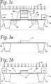
本発明の付加的な態様は、第1の組の堆積/注入プロセスの後に、付加的なゲートパターン形成工程を導入することを含む。本発明のこの実施形態においては、第2の電極堆積層もまた、ゲート電極の中にパターン形成されなければならないため、2つのゲートパターン形成工程が必要になる。2つのゲートパターン形成の手法は、2つのゲートパターンを重ねることが困難であるため、非対称的なトランジスタ構造が望まれる場合においてのみ用いられる。2つのゲートパターン形成工程においては、2つのゲートパターンを非対称的に設計することができ、非対称的な特性にわたり制御を与える。非対称重なり構造体及びノッチ形成されたゲート構造体といった2つの非対称構造体が述べられる。 An additional aspect of the present invention includes introducing an additional gate patterning step after the first set of deposition / implantation processes. In this embodiment of the invention, the second electrode deposition layer must also be patterned in the gate electrode, requiring two gate patterning steps. The two gate pattern formation methods are used only when an asymmetric transistor structure is desired because it is difficult to overlap the two gate patterns. In the two gate pattern formation steps, the two gate patterns can be designed asymmetrically, giving control over the asymmetric characteristics. Two asymmetric structures are described, an asymmetric overlap structure and a notched gate structure.
より具体的には、非対称重なりトランジスタは、2つのゲートパターン形成プロセスのシーケンスにより形成することができる。本発明のこの実施形態の一態様は、注入に対する必要条件が同様であるため、電極注入工程を用いてドレイン延長部層を形成できることである。本実施形態の付加的な態様は、2つのゲートパターンをずらすことにより、非対称重なりトランジスタ構造体を形成する能力である。このプロセスのシーケンスは、図3aないし図3cに示される。図3aにおいては、図1aからの基板がゲートパターン形成工程により処理されている。0.13μm技術ノードにおいては、このパターンに対するゲート長さは、約50ないし80nmである。この時点で、図3bに示されるようにフォトレジスト層(42)が適用されパターン形成されて、誘電体層13のドレイン延長部層38及び39を露出させる。浅いイオン注入工程が与えられて、ドレイン延長部(43)が露出されたソース及びドレイン領域に生成され、第1ゲート電極の露出表面がドーピングされることになる(44)。この注入に対する注入条件は、5.5keVで、約5×1015cm-2のドーズ量のデカボラン注入とすることができ、又はデカボランのようなホウ素又はホウ素クラスタによるプロセス等価の注入とすることができる。この時点で、フォトレジスト層(42)が通常の技術により除去され、第2のゲートの堆積(45)が与えられて、図3cに示される構造体が生成される。次いで、ゲート電極層がパターン形成されて、このパターンは、第1のゲートパターン層より大きく、これに対してずらされている。その結果もたらされるゲート電極スタックは図3dに示される。第1のゲート層を超える第2のゲート層の重なりは、図示されるように(46)トランジスタのソース側に制約することができる。このようにして、上でGhani他により述べられたように、ドレイン飽和電流IDSATを劣化させることなく、非常に小さいトランジスタを形成することができる。このプロセスは、図3eに示されるように、ゲート側壁スペーサ(51)の形成、及びPMOSトランジスタのみを露出するようにするフォトレジスト層(50)の適用及びパターン形成が続き、このようにして、前述の誘電体層13のドレイン領域38及びソース領域39が形成される。次いで、2keV、約5×1015cm-2のホウ素のイオンビーム(47)条件であるか、又はプロセス等価クラスタのイオン注入により、第2のイオン注入が行われる。図3eは、このイオン注入の浸透によるソース及びドレイン領域(48)、及びゲート電極における第2のイオン注入層の形成を示す。この時点で、非対称重なりトランジスタ構造が形成され、基板は、中間誘電体堆積、コンタクト形成、メタライゼーションなどによる通常のCMOS製造シーケンスで継続する。非対称重なりトランジスタの他の変形を本方法の変形により形成することができる。
More specifically, an asymmetric overlapping transistor can be formed by a sequence of two gate patterning processes. One aspect of this embodiment of the invention is that the drain extension layer can be formed using an electrode implantation process because the requirements for implantation are similar. An additional aspect of this embodiment is the ability to form an asymmetric overlapping transistor structure by shifting the two gate patterns. The sequence of this process is shown in FIGS. 3a-3c. In FIG. 3a, the substrate from FIG. 1a has been processed by a gate pattern formation step. At the 0.13 μm technology node, the gate length for this pattern is about 50 to 80 nm. At this point, a photoresist layer (42) is applied and patterned as shown in FIG. 3b to expose the drain extension layers 38 and 39 of the
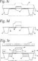
本発明の別の態様は、図4aないし図4eに示されるように本方法を適用することにより、ノッチ形成されたゲートトランジスタ構造体の形成に関する。このプロセスのシーケンスは、図1bに示されるように、第1ゲートの堆積及び第1ゲートの注入による基板の処理で開始する。この時点で、第1のゲート電極層がパターン形成される。このプロセスの次の工程は、パターン形成されたゲートスタックの外側の露出された半導体表面に第2のゲート誘電体(52)を与えることである。第2のゲート誘電体は、第1のゲート誘電体とは異なるものであり、その処理は、窒素のような種を既存のゲート誘電体の中に注入すること、高温でのアンモニアに対する露出のような既存の誘電体の化学的処理、既存の誘電体をなくして、異なる厚さの二酸化ケイ素のような異なるゲート誘電体又は異なる窒素含量をもつオキシナイトライド誘電体の再生、窒化ケイ素又はハフニウム又は酸化ジルコニウム又はケイ酸塩のような付加的なゲート誘電体層の堆積、又は、このような処理の組み合わせを含む様々なゲート誘電体処理工程のいずれかを含むことができる。第2のゲート誘電体処理工程は、第1のゲート誘電体とは異なるゲート誘電体を与えるため、第2のゲート領域のしきい値電圧は、第1のものとは異なるものになる。この時点での別の選択肢は、イオンビーム(64)及びしきい値調整注入層(65)により示されるような、第2のしきい値調整注入の適用である。このイオン注入は、いずれかの伝導性形式の非常に軽い1×1013cm-2の範囲のドーズ量とすることができる。第2のゲート誘電体と組み合わせて、この注入は、第2のゲート領域のしきい値電圧を設定することになる。 Another aspect of the present invention relates to the formation of a notched gate transistor structure by applying the method as shown in FIGS. 4a-4e. This process sequence begins with the processing of the substrate by deposition of the first gate and implantation of the first gate, as shown in FIG. 1b. At this point, the first gate electrode layer is patterned. The next step in this process is to provide a second gate dielectric (52) on the exposed semiconductor surface outside the patterned gate stack. The second gate dielectric is different from the first gate dielectric, and the process involves implantation of a species such as nitrogen into the existing gate dielectric, exposure to ammonia at high temperatures. Chemical treatment of existing dielectrics, such as eliminating existing dielectrics, regeneration of different gate dielectrics such as silicon dioxide of different thickness or oxynitride dielectrics with different nitrogen content, silicon nitride or hafnium Alternatively, it may include any of a variety of gate dielectric processing steps including deposition of additional gate dielectric layers such as zirconium oxide or silicate, or a combination of such processes. Since the second gate dielectric processing step provides a gate dielectric that is different from the first gate dielectric, the threshold voltage of the second gate region will be different from the first. Another option at this point is the application of a second threshold adjustment implant, as shown by the ion beam (64) and the threshold adjustment implant layer (65). This ion implantation can be a very light dose in the range of 1 × 10 13 cm −2 of either conductivity type. In combination with the second gate dielectric, this implantation will set the threshold voltage of the second gate region.
図4bに示されるように、処理は、第2のゲート電極堆積工程により継続して、これは、合計厚さが通常のものになるような厚さで堆積される。この堆積は、アモルファスシリコン又はポリシリコンとすることができる。次の工程は、図4cに示されるように、第2のゲート電極の堆積(54)のパターン形成である。最終的なトランジスタ構造体は、したがって、異なるゲート誘電体を有する2つの領域を含む。 As shown in FIG. 4b, processing continues with a second gate electrode deposition step, which is deposited at a thickness such that the total thickness is normal. This deposition can be amorphous silicon or polysilicon. The next step is the patterning of the second gate electrode deposition (54) as shown in FIG. 4c. The final transistor structure thus includes two regions with different gate dielectrics.
次に、フォトレジスト層(55)は、図4dに示されるように、PMOSデバイス(すなわち、ドレイン延長部64及び65)を露出させるように適用されパターン形成される。次いで、ドレイン延長部(57)が、ホウ素含有イオンビーム(56)の注入により形成される。この注入に対する典型的な条件は、500eVのエネルギ及び5×1014cm-2のドーズ量、又はプロセス等価パラメータをもつホウ素クラスタ注入である。この注入は、さらに、通常の方法により、ゲートスタック縁に対するドレイン延長部の自己位置合わせを達成する。この注入は、被覆範囲が与えられない限りは、浅いドーピング層(58)をゲート電極の表面上に形成する。この時点で、図4eに示されるように、フォトレジスト層(55)が剥離されて、絶縁側壁スペーサ(59)がゲート電極の側壁に形成される。新しいフォトレジスト層(62)が適用されパターン形成されて、ここでも、NMOS領域を保護し、PMOS領域を露出させる(すなわち、ソース及びドレイン領域66及び67のそれぞれを露出させる)。次に、イオンビーム(60)が注入されて、ソース及びドレイン領域(61)が形成される。注入は、さらに、ゲート電極のドーピング(63)を与える。この時点で、ノッチ形成されたゲートトランジスタ構造体が形成されて、この基板は、中間誘電体堆積、コンタクト形成、メタライゼーションなどによる通常のCMOS製造シーケンスで継続する。本方法の変形により、ノッチ形成されたゲートトランジスタの他の変形も形成することができる。
Next, a photoresist layer (55) is applied and patterned to expose the PMOS device (ie,
本発明の一態様は、第1の堆積厚さ、第1の注入深さ(注入エネルギ)、及び熱処理の組み合わせが、確実に、ゲート酸化膜に対するどのようなホウ素の浸透も生じないようにすることである。このことは、第1の堆積を非常に薄くすること、及び第1の注入を非常に浅くして、拡散を最小にするように熱処理を選択することを必要とする。本発明の一実施形態においては、クラスタイオンの注入を、約20nmの第1の堆積厚さまでの第1の注入工程及び熱処理のためのスパイクアニールに用いることができる。このプロセス工程の組み合わせは、ゲートのデプリーション及びゲート酸化膜に対するホウ素の浸透を最小にするのに必要な構造体を与える。典型的な条件は、20nmの第1の堆積厚さ、おおよそ5keVで、1×1014cm-2のドーズ量の第1のデカボラン注入、及び100℃の温度までのスパイクアニールを含む。この条件は、ゲート誘電体に対してどのようなホウ素の浸透も生じないようにすることを確実にするものとなる。 One aspect of the present invention ensures that the combination of the first deposition thickness, the first implantation depth (implantation energy), and the heat treatment does not cause any boron penetration into the gate oxide. That is. This requires that the first deposition be very thin, and that the first implant be very shallow and the heat treatment be selected to minimize diffusion. In one embodiment of the present invention, cluster ion implantation can be used for a first implantation step to a first deposition thickness of about 20 nm and a spike anneal for heat treatment. This combination of process steps provides the necessary structure to minimize gate depletion and boron penetration into the gate oxide. Typical conditions include a first deposition thickness of 20 nm, a first decaborane implant with a dose of 1 × 10 14 cm −2 at approximately 5 keV, and a spike anneal to a temperature of 100 ° C. This condition ensures that no boron penetration into the gate dielectric occurs.
図5は、適切な注入条件を達成することができることを明示する。このシミュレーションは、例えば、1985年ニューヨークのPrgamon PressのJ.Ziegler他による「The Stopping and Range of Ions in Solids」に述べられるような、材料の中に注入されたイオンの深さ及び分散を計算するプログラム、SRIM2000を用いて行われた。この実施例においては、公称注入パラメータは、2つの注入プロセスによりもたらされる深さ特性を定めるようにモデル化される。第1の堆積(71)は、15nm厚さのポリシリコン堆積としてモデル化される。第1の注入条件は、1×1015cm-2のドーズ量の500eVのホウ素注入とすることができ、結果としてもたらされる特性(72)は図6に示されるように、どの注入も(<0.1%)ゲート酸化膜界面(75)に到達せず、明らかに、ゲート誘電体を通って下にあるシリコンの中に入るものはなかった。第2の堆積(73)は、125nmのポリシリコンの堆積としてモデル化され、この後に、2keVのエネルギ及び5×1015cm-2のドーズ量のホウ素注入が続き、特性(74)が結果としてもたらされた。第2の注入の特性(74)は、完全にゲート電極層に含まれる。NMOSデバイスにおいては、ヒ素イオン注入を用いることができ、ヒ素はより高質量の原子であるため、その浸透深さは少なく、したがって、ゲート浸透に対するリスクは存在しない。 FIG. 5 demonstrates that appropriate injection conditions can be achieved. This simulation is described, for example, in J. 1985 by Prgamon Press in New York. This was done using SRIM2000, a program that calculates the depth and dispersion of ions implanted in a material, as described in “The Stopping and Range of Ions in Solids” by Ziegler et al. In this example, the nominal injection parameters are modeled to define the depth characteristics provided by the two injection processes. The first deposition (71) is modeled as a 15 nm thick polysilicon deposition. The first implant condition can be a 500 eV boron implant with a dose of 1 × 10 15 cm −2 , and the resulting characteristics (72) are as shown in FIG. 0.1%) did not reach the gate oxide interface (75) and apparently nothing entered the underlying silicon through the gate dielectric. The second deposition (73) was modeled as a 125 nm polysilicon deposition, followed by a 2 keV energy and 5 × 10 15 cm −2 dose of boron implantation, resulting in a characteristic (74). It was brought. The second implantation characteristic (74) is completely contained in the gate electrode layer. In NMOS devices, arsenic ion implantation can be used, and since arsenic is a higher mass atom, its penetration depth is small and therefore there is no risk for gate penetration.
超浅接合部の形成
本発明の別の態様は、所望のドーパントを半導体基板の表面上の誘電体層の中に注入して、該ドーパントを該誘電体層から外に、該半導体基板の中に拡散して、接合部を形成することにより、該半導体基板に超浅接合部を形成することに関する。第2の種をドーパントと同時にであるか又はこれの後に誘電体層の中に注入して、誘電体/ドーパントシステムの拡散特性を改変することができる。このような方法の例は、シリコンウエハ上の二酸化ケイ素層の中にホウ素水素化クラスタを注入することであり、ここでは、水素が、酸化物層を通るホウ素の拡散を向上させ、したがって、ホウ素による超浅接合部の形成をより効率的なものにする。
Formation of Ultra-Shallow Junction Another aspect of the present invention is to implant a desired dopant into a dielectric layer on the surface of a semiconductor substrate so that the dopant is out of the dielectric layer and into the semiconductor substrate. To form an ultra shallow junction in the semiconductor substrate by forming a junction. The second species can be implanted into the dielectric layer simultaneously with or after the dopant to modify the diffusion characteristics of the dielectric / dopant system. An example of such a method is injecting boron hydride clusters into a silicon dioxide layer on a silicon wafer, where hydrogen improves the diffusion of boron through the oxide layer and thus boron To make the formation of ultra-shallow junctions more efficient.
このプロセスは、図6に示されるように、半導体基板1で開始する。典型的には、半導体基板はシリコンウエハであるが、III−V半導体基板であってもよい。さらに、半導体基板は、典型的には、或る程度までドーピングされているが、この半導体基板はドーピングされたn型と仮定される。この半導体基板の表面上には、薄い誘電体層2がある。この誘電体層は、典型的には、二酸化ケイ素であるか又は窒化ケイ素であるが、他の材料も可能である。誘電体層の厚さは最適化されるが、5ないし20nmの範囲の厚さである傾向がある。誘電体層は、2つの材料間の界面(3)において半導体基板(1)と接触する。
This process begins with a semiconductor substrate 1 as shown in FIG. Typically, the semiconductor substrate is a silicon wafer, but may be a III-V semiconductor substrate. Furthermore, the semiconductor substrate is typically doped to some extent, but this semiconductor substrate is assumed to be doped n-type. On the surface of the semiconductor substrate is a
図7に示されるように、イオンビーム(4)は、イオン注入層(5)が完全に誘電体層の中に含まれるように、十分に低いエネルギで、表面に向けられる。イオンビーム(4)は、ホウ素クラスタイオンのような単一注入であるか、又は、ホウ素注入の後に水素注入が続く一連の注入のいずれかを表すことができる。ドーパント種注入層は、注入層5に示されるように、完全に誘電体層の中に含まれることが望ましい。例えば、誘電体層が二酸化ケイ素であり、厚さが20nmである場合には、500eV又はこれより少ないホウ素の注入は、完全に、該誘電体層の中に含まれることになる。第2の注入種もまた、完全に誘電体層の中に含まれて、その効率性を増加させることが望ましいが、半導体基板に入るわずかな第2の種は、その結果もたらされる接合部に対しては影響がない。次に、熱処理が適用されて、ここでは、温度及び時間が、誘電体層2から外に、界面3を通ってドーパント種が拡散するのに十分な拡散を与えるように最適化されて、図8に示されるように、半導体基板(1)に浅い接合部6を形成する。
As shown in FIG. 7, the ion beam (4) is directed to the surface with sufficiently low energy so that the ion implantation layer (5) is completely contained within the dielectric layer. The ion beam (4) can represent either a single implant, such as a boron cluster ion, or a series of implants followed by a hydrogen implant followed by a hydrogen implant. The dopant seed implant layer is preferably completely contained within the dielectric layer as shown in implant layer 5. For example, if the dielectric layer is silicon dioxide and the thickness is 20 nm, an implant of boron of 500 eV or less will be completely contained in the dielectric layer. It is desirable that the second implant species also be fully contained in the dielectric layer to increase its efficiency, but the few second species that enter the semiconductor substrate will be in the resulting junction. There is no effect on it. Next, a heat treatment is applied, where the temperature and time are optimized to provide sufficient diffusion out of the
この方法は、直接、半導体基板の中に注入することを魅力あるものにする幾つかの特徴を有する。第1に、注入プロセスは、必ず、製造される接合部の良好な電気特性を達成するのに好ましくない結晶の欠陥を半導体基板の中に導入する。注入の損傷を誘電体層に含むことは、製造される半導体デバイス及び接合部の形成プロセス自体の両方に有益である。これは、注入の欠陥は、非結晶性であるために誘電体層の劣化をもたらすことがなく、この欠陥は、該誘電体層を通るドーパントの拡散を高めることになるためである。 This method has several features that make it attractive to implant directly into a semiconductor substrate. First, the implantation process necessarily introduces crystal defects into the semiconductor substrate that are undesirable for achieving good electrical properties of the manufactured joint. Including implant damage in the dielectric layer is beneficial for both the semiconductor device being fabricated and the process of forming the junction itself. This is because implantation defects do not cause degradation of the dielectric layer because they are non-crystalline, and this defect will increase dopant diffusion through the dielectric layer.
上述の方法は、注入ドーパントを電気作動させるのに用いられる熱処理プロセスに対する制約を緩和するものである。熱処理の目的は、ドーパントを半導体格子内の代理位置の中に置いて、該ドーパントを半導体原子と結合させて、したがって、半導体システム内でその電気作動を得るようにすることである。通常のプロセスにおいては、注入ドーパントは、ほとんど格子間の位置を占め、該ドーパントを代理の電気作動位置に置くには高温のアニーリング工程が必要になる。この高温プロセスは、注入ドーパントの実質的な拡散を可能にするが、これは、超浅接合部の形成には不利に作用する。通常のプロセスにおいては、最適化は、スパイクアニールにより得られ、ここでは、アニーリング工程の温度は、最高温度まで上げられ、直ちに下に戻されて、最小の拡散で電気作動を達成する。提案されたプロセスにおいては、拡散によりその位置に到達した半導体内のすべてのドーパントは、拡散プロセスが代理のものであるために、これは代理のものであることを意味する。したがって、ここでは、アニールは、ドーパントが誘電体層を通り、半導体基板の中までにだけ拡散することが選択されるため、異なるアニーリング工程の最適化が要求される。これは、スパイクアニールではなく、有限の時間で低温で、より良好に達成されることが予想される。 The method described above alleviates the constraints on the heat treatment process used to electrically operate the implanted dopant. The purpose of the heat treatment is to place the dopant in a surrogate position in the semiconductor lattice to bond the dopant with the semiconductor atoms and thus obtain its electrical actuation within the semiconductor system. In normal processes, implanted dopants occupy most of the interstitial positions, and a high temperature annealing step is required to place the dopants in surrogate electrical actuation positions. This high temperature process allows substantial diffusion of implanted dopants, which adversely affects ultra shallow junction formation. In normal processes, optimization is obtained by spike annealing, where the temperature of the annealing step is raised to the highest temperature and immediately returned to achieve electrical operation with minimal diffusion. In the proposed process, all dopants in the semiconductor that have reached their position by diffusion mean that this is a surrogate because the diffusion process is surrogate. Therefore, here, annealing is selected to allow the dopant to diffuse only through the dielectric layer and into the semiconductor substrate, so that different annealing processes are required to be optimized. This is expected to be better achieved at low temperatures in a finite time rather than spike annealing.
本発明によるプロセスは、上のSchmitzの文献により述べられるものより効率的であり、例えば、水素のような第2の種の導入を含む。ホウ素を二酸化ケイ素に拡散することは、ホウ素をシリコンに拡散させることにより遅く、高濃度接合部の形成の効率に対して制限を呈する。この制限を管理する1つの方法は、水素の導入により誘電体における拡散率を向上させることである。Fairにより、水素の存在は、拡散率を2倍向上できることが示されている。水素の注入は、通常は、拡散中に、雰囲気から水素を導入する代替的手法に対して魅力的なプロセスである。アニーリングプロセスは、高温(>800C)であり、水素は、空気との接触により可燃性になるため、これをアニーリング用雰囲気として用いることは危険である。半導体技術において水素の拡散を行う通常の手段は、はるかに安全な水素及び窒素の混合物で構成された雰囲気を用いることである。しかし、窒素の効果は、二酸化ケイ素におけるホウ素の拡散を後退させるものであるため、安全な混合物は、あまり利益をもたらさない。水素の注入は、二酸化ケイ素におけるホウ素の拡散を向上させるのに非常に安全で効率的な方法である。 The process according to the invention is more efficient than that described by the Schmitz reference above and involves the introduction of a second species such as hydrogen, for example. Diffusion of boron into silicon dioxide is slowed by diffusing boron into silicon, and presents a limitation on the efficiency of high concentration junction formation. One way to manage this limitation is to improve the diffusivity in the dielectric by introducing hydrogen. Fair shows that the presence of hydrogen can double the diffusivity. Hydrogen injection is an attractive process for alternative approaches that typically introduce hydrogen from the atmosphere during diffusion. The annealing process is hot (> 800C) and hydrogen becomes flammable upon contact with air, so it is dangerous to use it as an annealing atmosphere. The usual means of hydrogen diffusion in semiconductor technology is to use an atmosphere composed of a much safer mixture of hydrogen and nitrogen. However, since the effect of nitrogen reverses the diffusion of boron in silicon dioxide, a safe mixture offers little benefit. Hydrogen injection is a very safe and efficient way to improve boron diffusion in silicon dioxide.
本発明のさらに別の態様は、通常のプロセスにおける注入制約の多くを緩和することである。これらの制約は、注入ドーズ量及び注入エネルギを含む。この方法の一態様は、より高いドーズ量の注入の有用性が高められることである。注入が半導体基板の中に直接行われる通常のプロセスにおいては、ドーパントを無効なものにする種々の材料の代替的な位相の形成のために、効率的に注入することができるドーパント量には制限がある。例えば、シリコンの中にホウ素を注入する場合には、アニーリング温度で、注入濃度がホウ素の固溶度を超える場合には、過剰なホウ素がシリコンホウ化物として析出し、ホウ素を電気的に不作動なものにして回復を非常に困難にする。この機構は、通常プロセスにより達成することができる電気作動ホウ素の量に上限を設ける。提案された方法においては、注入ドーパントは、どのような代替的な位相材料も観察されていないアモルファス誘電体層の中に進む。したがって、すべての注入ホウ素は、誘電体層を通る拡散特性の確立により、超浅接合部の形成プロセスに貢献する。拡散特性が、半導体におけるホウ素の固溶度を超える濃度を含有することは、例えば、半導体表面に拡散するドーパントの流れを増加させることができるため、このプロセスに非常に有益である。提案された方法の別の態様は、表面誘電体層の中への注入は、注入エネルギを増加できることである。通常の方法は、注入深さは、超浅接合部を確立する際の重要な要因であるため、極めて低い注入エネルギの必要条件がある。提案されたプロセスにおいては、注入エネルギは、プロセスを最適化するように選択することができる誘電体層の厚さに関連する。酸化物層を薄く維持し、低エネルギの注入を利用するのは望ましいことであるが、この選択は、直接、接合部の深さに影響を与えるのではなく、拡散をより有効にするものである。注入の生産性は、直接、注入エネルギに関連するため、提案された方法が好ましい。 Yet another aspect of the present invention is to relax many of the implantation constraints in normal processes. These constraints include implantation dose and implantation energy. One aspect of this method is that the usefulness of higher dose implantation is enhanced. In the normal process where implantation is performed directly into the semiconductor substrate, the amount of dopant that can be efficiently implanted is limited due to the formation of alternative phases of various materials that render the dopant ineffective. There is. For example, when boron is implanted into silicon, if the implantation concentration exceeds the solid solubility of boron at the annealing temperature, excess boron precipitates as silicon boride and the boron is electrically deactivated. And make recovery very difficult. This mechanism places an upper limit on the amount of electrically actuated boron that can be achieved by the normal process. In the proposed method, the implanted dopant goes into an amorphous dielectric layer where no alternative phase material has been observed. Thus, all implanted boron contributes to the ultra-shallow junction formation process by establishing diffusion properties through the dielectric layer. It is very beneficial to this process that the diffusion properties contain a concentration that exceeds the solid solubility of boron in the semiconductor, for example, because it can increase the flow of dopant that diffuses to the semiconductor surface. Another aspect of the proposed method is that implantation into the surface dielectric layer can increase the implantation energy. Conventional methods have very low implantation energy requirements because implantation depth is an important factor in establishing ultra-shallow junctions. In the proposed process, the implantation energy is related to the thickness of the dielectric layer that can be selected to optimize the process. While it is desirable to keep the oxide layer thin and utilize low energy implants, this option does not directly affect the junction depth, but makes diffusion more effective. is there. The proposed method is preferred because the productivity of implantation is directly related to the implantation energy.
提案された方法の別の態様は、第2の種の注入を、この種の幾つかの有害な影響を避ける手段として用いることである。具体的には、水素によるホウ素拡散の向上を例に用いると、アニールが水素雰囲気で行われる場合に生じる、ゲート酸化物層を通るホウ素の拡散を向上させることは有害であり、すなわち任意の高温処理中に過剰な水素が得られることになる。提案された方法においては、水素の注入は、ホウ素の拡散が望まれる正確な領域にこれを置き、これは、回路の他の領域からマスクされる。本方法のさらに別の態様は、あらゆる過剰な水素は、他に領域に拡散することが可能であり、望ましくない場所での拡散を有害に向上させるため、十分に足る水素だけが導入されることである。向上された影響は、水素が拡散ホウ素に堆積し、クラスタとして拡散するものと信じられているため、1/1の比率が、プロセスの中に導入される水素の理想的な量である。注入により、この水素は、ホウ素が存在し拡散する正確な量で置かれる。水素雰囲気におけるアニーリングのような通常の方法は、大量の水素を半導体基板のすべての領域の中に導入して、望ましくない領域での拡散を高めるようになる。提案された方法のさらに別の実施形態は、2つの種を別々に注入して、第2の種を第1の種とは異なるようにマスクして、該第1の種が注入された或る領域だけが向上された拡散を受けるようにする選択を可能にすることである。このようにして、ソース/ドレイン延長部の2つの異なる最適化は、第2の注入をマスクするだけで得ることができる。このことは、今日の半導体製造プロセスに典型的な異なる特性をもつ種々のトランジスタが、単一のプロセスの流れで製造されるプロセスに有益になる。 Another aspect of the proposed method is to use a second type of injection as a means to avoid some of the harmful effects of this type. Specifically, using the boron diffusion enhancement by hydrogen as an example, improving the boron diffusion through the gate oxide layer, which occurs when annealing is performed in a hydrogen atmosphere, is detrimental, i.e., at any high temperature. Excess hydrogen will be obtained during processing. In the proposed method, the hydrogen implantation places it in the exact area where boron diffusion is desired, which is masked from other areas of the circuit. Yet another aspect of the method is that any excess hydrogen can diffuse to other regions and only enough hydrogen is introduced to deleteriously improve diffusion in undesirable locations. It is. The improved effect is believed to be that hydrogen deposits on the diffused boron and diffuses as clusters, so a 1/1 ratio is the ideal amount of hydrogen introduced into the process. By implantation, this hydrogen is placed in the exact amount in which boron is present and diffuses. Conventional methods such as annealing in a hydrogen atmosphere introduce a large amount of hydrogen into all regions of the semiconductor substrate to increase diffusion in undesirable regions. Yet another embodiment of the proposed method is that the two species are implanted separately and the second species is masked differently from the first species so that the first species is implanted or It is possible to make a selection so that only the areas that are subjected to improved diffusion. In this way, two different optimizations of the source / drain extension can be obtained simply by masking the second implant. This is beneficial for processes in which a variety of transistors with different characteristics typical of today's semiconductor manufacturing processes are manufactured in a single process flow.
本発明のこの態様においては、ドーパント注入をディセル式注入機で行うことは極めて望ましくない。このことは、すべてのディセル注入機のビームには、ある程度のエネルギ汚染が存在するためである。市販のシステムにおいては、このエネルギ汚染は、生産可能プロセスに対して0.1ないし1.0%の範囲である。通常の浅い接合部プロセスにおいては、より高いエネルギにおけるビーム部分であるこの汚染は、半導体基板の中により深く浸透して、注入形状にテールを形成し、このことは、一般に、プロセスの最適化において管理することができる。提案されたプロセスにおいては、より高いエネルギのビームは、表面誘電体層を通り、半導体基板の中に浸透して、望ましくない注入領域を形成するため、この汚染はより有害なものである。提案されたプロセスは、通常の方法より高いドーズ量を使用する傾向があるため、半導体における汚染濃度は、通常の場合に比例して高くなり、問題を悪化させる。したがって、本方法の好ましい実施形態は、関心のある両方の種が、より高いエネルギ汚染の存在なしで、同時に注入されるドリフトモードにおけるクラスタ注入である。 In this aspect of the invention, it is highly undesirable to perform the dopant implantation with a decel implanter. This is because some energy contamination is present in the beams of all the decelerators. In commercial systems, this energy contamination is in the range of 0.1 to 1.0% with respect to the producible process. In normal shallow junction processes, this contamination, which is the beam part at higher energy, penetrates deeper into the semiconductor substrate, forming a tail in the implant shape, which is generally a process optimization. Can be managed. In the proposed process, this contamination is more detrimental because the higher energy beam penetrates the surface dielectric layer and penetrates into the semiconductor substrate, creating an undesirable implant region. Since the proposed process tends to use higher doses than the usual method, the contamination concentration in the semiconductor becomes proportionally higher and exacerbates the problem. Thus, a preferred embodiment of the method is cluster injection in drift mode where both species of interest are injected simultaneously without the presence of higher energy contamination.
本発明が、幾つかの実施形態と併せて述べられた。本発明は、これに限定されるものではない。例えば、当業者には、種々の修正、改変、改良、及びこれらの組み合わせが可能であることが明らかであろう。 The invention has been described in conjunction with several embodiments. The present invention is not limited to this. For example, it will be apparent to those skilled in the art that various modifications, alterations, improvements, and combinations thereof are possible.
明らかに、本発明の多数の修正及び変形が、上述の教示の観点から可能である。したがって、本発明は、別の方法により特に上述されたものではなく、特許請求の範囲内で実施することができることが理解されるであろう。 Obviously, many modifications and variations of the present invention are possible in light of the above teachings. Accordingly, it will be understood that the invention is not specifically described by other methods and can be practiced within the scope of the appended claims.
特許請求され、特許状によりカバーされることが望まれるものが上述される。 What has been claimed and desired to be covered by the patent is described above.
Claims (30)
(a)第1のゲート電極層を前記第1の誘電体層に堆積させる工程と、
(b)前記第1のゲート電極層をドーピングして、ドーピングされた第1のゲート電極層を形成する工程と、
(c)第2のゲート電極層を前記ドーピングされた第1のゲート電極層の上に堆積させる工程と、
(d)前記第2のゲート電極層をドーピングする工程と、
(e)この構造体を熱処理して、ドーパント材料を活性化する工程と、
を含む方法。 A method of forming a gate electrode of a metal oxide semiconductor device having a substrate, having a well and opposing trench isolation portions formed thereon and having a first dielectric layer formed thereon, comprising:
(A) depositing a first gate electrode layer on the first dielectric layer;
(B) doping the first gate electrode layer to form a doped first gate electrode layer;
(C) depositing a second gate electrode layer on the doped first gate electrode layer;
(D) doping the second gate electrode layer;
(E) heat treating the structure to activate the dopant material;
Including methods.
(a)ウェル及び対向するトレンチ隔離部分を前記第1の基板に形成する工程と、
(b)その上に第1の誘電体層を堆積させる工程と、
(c)第1のゲート電極層を前記第1の誘電体層の上に堆積させる工程と、
(d)前記第1のゲート電極層をドーピングして、ドーピングされた第1のゲート電極層を形成する工程と、
(e)第2のゲート電極層を前記ドーピングされた第1のゲート電極層の上に堆積させる工程と、
(f)前記ドーピングされた第1のゲート電極層と前記第2のゲート電極層との組み合わせからゲートスタックを形成して、前記第1の誘電体層の露出部分を生じさせる工程と、
(g)第1のフォトレジストをパターン形成して、前記第1の誘電体層上の前記トレンチ隔離部分に隣接するドレイン延長部領域を露出させる工程と、
(h)前記ゲートスタックの露出部分と前記第1の誘電体層の露出部分とをドーピングして、ドレイン延長部を前記ウェル内の前記トレンチ隔離部分と前記ゲートスタックとの間に形成する工程と、
(i)前記第1のフォトレジストを除去し、第2のフォトレジストをパターン形成して、前記ゲートスタックの両側に隣接するスペーサを形成し、ドレイン及びソース領域を定める前記第1の誘電体層の部分を露出させる工程と、
(j)前記第1の誘電体層の前記露出部分をドーピングして、前記ウェル内にソース及びドレイン層を形成する工程と、
(k)前記第2のフォトレジスト層を除去する工程と、
(l)注入ドーパントを拡散させるために熱処理を与えて、前記注入ドーパントが、前記第1の誘電体層から外に、前記ウェルの中に拡散するようにする工程と、
を含む方法。 A method of forming a metal oxide semiconductor (MOS) device having a substrate, comprising:
(A) forming a well and opposing trench isolation in the first substrate;
(B) depositing a first dielectric layer thereon;
(C) depositing a first gate electrode layer on the first dielectric layer;
(D) doping the first gate electrode layer to form a doped first gate electrode layer;
(E) depositing a second gate electrode layer on the doped first gate electrode layer;
(F) forming a gate stack from a combination of the doped first gate electrode layer and the second gate electrode layer to produce an exposed portion of the first dielectric layer;
(G) patterning a first photoresist to expose a drain extension region adjacent to the trench isolation on the first dielectric layer;
(H) doping an exposed portion of the gate stack and an exposed portion of the first dielectric layer to form a drain extension between the trench isolation portion in the well and the gate stack; ,
(I) removing the first photoresist, patterning a second photoresist, forming adjacent spacers on opposite sides of the gate stack, and defining the drain and source regions of the first dielectric layer Exposing the portion of
(J) doping the exposed portion of the first dielectric layer to form source and drain layers in the well;
(K) removing the second photoresist layer;
(L) providing a heat treatment to diffuse the implanted dopant such that the implanted dopant diffuses out of the first dielectric layer and into the well;
Including methods.
(a)ウェル及び対向するトレンチ隔離部分を前記基板に形成する工程と、
(b)その上に第1の誘電体層を堆積させる工程と、
(c)第1のゲート電極層を前記第1の誘電体層の上に堆積させる工程と、
(d)前記第1のゲート電極層からゲートスタックを形成して、前記第1の誘電体層の露出部分を残すようにする工程と、
(e)第1のフォトレジスト層をパターン形成して、前記第1の誘電体層のドレイン延長部領域を露出させる工程と、
(f)ドレイン延長部層及び前記ウェルを形成する前記ドレイン延長部領域をドーピングする工程と、
(g)前記第1のフォトレジスト層を除去する工程と、
(h)第2のゲート電極層を堆積させる工程と、
(i)前記第2のゲート電極スタックを、前記第1のゲート電極層から形成された前記ゲートスタックとずらして、かつこれより大きく形成する工程と、
(j)第2のフォトレジスト層をパターン形成して、前記第2のゲート電極スタックに隣接するスペーサを形成し、ドレイン及びソース領域を定める工程と、
(k)前記ドレイン及びソース領域をドーピングして、ドレイン及びソース層を前記ウェルに形成する工程と、
(l)前記第2のフォトレジスト層を除去する工程と、
(m)熱処理を与えて、前記注入ドーパントが前記ドーピング工程により注入された材料を活性化させるようにする工程と、
を含む方法。 A method of forming a metal oxide semiconductor device having a substrate, comprising:
(A) forming a well and opposing trench isolation in the substrate;
(B) depositing a first dielectric layer thereon;
(C) depositing a first gate electrode layer on the first dielectric layer;
(D) forming a gate stack from the first gate electrode layer to leave an exposed portion of the first dielectric layer;
(E) patterning a first photoresist layer to expose a drain extension region of the first dielectric layer;
(F) doping the drain extension layer forming the drain extension layer and the well;
(G) removing the first photoresist layer;
(H) depositing a second gate electrode layer;
(I) forming the second gate electrode stack so as to be shifted from and larger than the gate stack formed from the first gate electrode layer;
(J) patterning a second photoresist layer to form spacers adjacent to the second gate electrode stack and defining drain and source regions;
(K) doping the drain and source regions to form drain and source layers in the well;
(L) removing the second photoresist layer;
(M) providing a heat treatment so that the implanted dopant activates the material implanted by the doping step;
Including methods.
(a)ウェル及び対向するトレンチ隔離部分を前記基板に形成する工程と、
(b)その上に第1の誘電体層を堆積させる工程と、
(c)第1のゲート電極層を前記第1の誘電体層の上に堆積させる工程と、
(d)前記第1のゲート電極層から初期ゲートスタックを形成して、前記第1の誘電体層の露出部分を残すようにする工程と、
(e)前記ゲートスタックと前記第1の誘電体層の前記露出表面とをドーピングする工程と、
(f)前記第1の誘電体層とは異なる第2のゲート誘電体層を該第1の誘電体層の前記露出表面の上に堆積させる工程と、
(g)第2のゲート電極堆積層を、前記初期ゲートスタック及び前記第2の誘電体層の上部に堆積させる工程と、
(h)前記第2のゲート電極の堆積から最終的なゲートスタックを形成する工程と、
(i)第1のフォトレジストをパターン形成して、前記最終的なゲートスタック及びドレイン延長部領域を露出させる工程と、
(j)前記最終的なゲートスタック及び前記ドレイン延長部領域をドーピングする工程と、
(k)前記第1のフォトレジストを除去する工程と、
(l)第2のフォトレジストをパターン形成して、前記最終的なゲートスタックに隣接する側壁スペーサを形成し、前記ドレイン及びソース領域を露出させる工程と、
(m)前記ドレイン及びソース領域及び前記最終的なゲート電極スタックをドーピングして、ドレイン及びソース層を前記ウェルに形成する工程と、
(n)前記第2のフォトレジスト層を除去する工程と、
(o)熱処理を与えて、前記ドーピング工程により注入された材料を活性化させる工程と、
を含む方法。 A method of forming a metal oxide semiconductor (MOS) device having a substrate, comprising:
(A) forming a well and opposing trench isolation in the substrate;
(B) depositing a first dielectric layer thereon;
(C) depositing a first gate electrode layer on the first dielectric layer;
(D) forming an initial gate stack from the first gate electrode layer to leave an exposed portion of the first dielectric layer;
(E) doping the gate stack and the exposed surface of the first dielectric layer;
(F) depositing a second gate dielectric layer different from the first dielectric layer on the exposed surface of the first dielectric layer;
(G) depositing a second gate electrode deposition layer on top of the initial gate stack and the second dielectric layer;
(H) forming a final gate stack from the deposition of the second gate electrode;
(I) patterning a first photoresist to expose the final gate stack and drain extension region;
(J) doping the final gate stack and the drain extension region;
(K) removing the first photoresist;
(L) patterning a second photoresist to form sidewall spacers adjacent to the final gate stack and exposing the drain and source regions;
(M) doping the drain and source regions and the final gate electrode stack to form drain and source layers in the well;
(N) removing the second photoresist layer;
(O) applying a heat treatment to activate the material implanted by the doping step;
Including methods.
(a)誘電体層を前記基板上に堆積させる工程と、
(b)前記誘電体層をドーピングする工程と、
(c)熱処理を与えて、前記熱処理による注入イオンを前記基板の中に拡散させて浅い接合部を形成するようにする工程と、
を含む方法。 A process for forming an ultra-shallow junction as an integral part of a semiconductor device on a semiconductor substrate,
(A) depositing a dielectric layer on the substrate;
(B) doping the dielectric layer;
(C) applying a heat treatment to diffuse implanted ions by the heat treatment into the substrate to form a shallow junction;
Including methods.
Applications Claiming Priority (3)
| Application Number | Priority Date | Filing Date | Title |
|---|---|---|---|
| US39180202P | 2002-06-26 | 2002-06-26 | |
| US39202302P | 2002-06-26 | 2002-06-26 | |
| PCT/US2003/019085 WO2004003970A2 (en) | 2002-06-26 | 2003-06-18 | A semiconductor device and method of fabricating a semiconductor device |
Related Child Applications (1)
| Application Number | Title | Priority Date | Filing Date |
|---|---|---|---|
| JP2010045361A Division JP5437112B2 (en) | 2002-06-26 | 2010-03-02 | Method for forming gate electrode of metal oxide semiconductor device and method for forming metal oxide semiconductor device |
Publications (1)
| Publication Number | Publication Date |
|---|---|
| JP2005531158A true JP2005531158A (en) | 2005-10-13 |
Family
ID=30003212
Family Applications (2)
| Application Number | Title | Priority Date | Filing Date |
|---|---|---|---|
| JP2004517659A Pending JP2005531158A (en) | 2002-06-26 | 2003-06-18 | Semiconductor device and semiconductor device manufacturing method |
| JP2010045361A Expired - Fee Related JP5437112B2 (en) | 2002-06-26 | 2010-03-02 | Method for forming gate electrode of metal oxide semiconductor device and method for forming metal oxide semiconductor device |
Family Applications After (1)
| Application Number | Title | Priority Date | Filing Date |
|---|---|---|---|
| JP2010045361A Expired - Fee Related JP5437112B2 (en) | 2002-06-26 | 2010-03-02 | Method for forming gate electrode of metal oxide semiconductor device and method for forming metal oxide semiconductor device |
Country Status (7)
| Country | Link |
|---|---|
| US (2) | US7723233B2 (en) |
| EP (1) | EP1540720A4 (en) |
| JP (2) | JP2005531158A (en) |
| KR (2) | KR100683594B1 (en) |
| CN (2) | CN101055838B (en) |
| AU (1) | AU2003261078A1 (en) |
| WO (1) | WO2004003970A2 (en) |
Cited By (2)
| Publication number | Priority date | Publication date | Assignee | Title |
|---|---|---|---|---|
| WO2008156182A1 (en) * | 2007-06-18 | 2008-12-24 | Nec Corporation | Semiconductor device and method for manufacturing the same |
| JP2011198937A (en) * | 2010-03-18 | 2011-10-06 | Renesas Electronics Corp | Method of manufacturing semiconductor device |
Families Citing this family (24)
| Publication number | Priority date | Publication date | Assignee | Title |
|---|---|---|---|---|
| AU2003261078A1 (en) * | 2002-06-26 | 2004-01-19 | Semequip Inc. | A semiconductor device and method of fabricating a semiconductor device |
| KR100788472B1 (en) * | 2002-06-26 | 2007-12-24 | 세미이큅, 인코포레이티드 | Vapor source for an ion source |
| US6686595B2 (en) * | 2002-06-26 | 2004-02-03 | Semequip Inc. | Electron impact ion source |
| JP2005236210A (en) * | 2004-02-23 | 2005-09-02 | Ricoh Co Ltd | Standard cell layout, standard cell library, semiconductor integrated circuit and its design method |
| KR100694660B1 (en) * | 2006-03-08 | 2007-03-13 | 삼성전자주식회사 | Transistor and method of manufacturing the same |
| US7435638B2 (en) * | 2006-05-26 | 2008-10-14 | Texas Instruments Incorporated | Dual poly deposition and through gate oxide implants |
| JP4560820B2 (en) * | 2006-06-20 | 2010-10-13 | エルピーダメモリ株式会社 | Manufacturing method of semiconductor device |
| CN101197284B (en) * | 2006-12-05 | 2010-06-02 | 上海华虹Nec电子有限公司 | Production method of high voltage asymmetric lateral structure diffusion type field effect tube |
| JP5220549B2 (en) * | 2008-10-20 | 2013-06-26 | 本田技研工業株式会社 | Stator structure of outer rotor type multipolar generator |
| JP2010199520A (en) * | 2009-02-27 | 2010-09-09 | Renesas Electronics Corp | Semiconductor laser, and method of manufacturing the same |
| KR101129028B1 (en) | 2010-03-24 | 2012-03-23 | 주식회사 하이닉스반도체 | Method for passivation annealing process in semiconductor device |
| CN101834141B (en) * | 2010-04-28 | 2015-03-04 | 复旦大学 | Preparation method of asymmetrical source drain field effect transistor |
| CN102468147B (en) * | 2010-11-01 | 2017-11-28 | 中芯国际集成电路制造(上海)有限公司 | A kind of method of forming gate of semiconductor devices |
| US8598025B2 (en) * | 2010-11-15 | 2013-12-03 | Varian Semiconductor Equipment Associates, Inc. | Doping of planar or three-dimensional structures at elevated temperatures |
| KR20120107762A (en) | 2011-03-22 | 2012-10-04 | 삼성전자주식회사 | Methods of fabricating semiconductor devices |
| US8580664B2 (en) | 2011-03-31 | 2013-11-12 | Tokyo Electron Limited | Method for forming ultra-shallow boron doping regions by solid phase diffusion |
| US8569158B2 (en) | 2011-03-31 | 2013-10-29 | Tokyo Electron Limited | Method for forming ultra-shallow doping regions by solid phase diffusion |
| US9263272B2 (en) | 2012-04-24 | 2016-02-16 | Taiwan Semiconductor Manufacturing Company, Ltd. | Gate electrodes with notches and methods for forming the same |
| US9673245B2 (en) * | 2012-10-01 | 2017-06-06 | Taiwan Semiconductor Manufacturing Company, Ltd. | Implant isolated devices and method for forming the same |
| US9355888B2 (en) | 2012-10-01 | 2016-05-31 | Taiwan Semiconductor Manufacturing Company, Ltd. | Implant isolated devices and method for forming the same |
| US20140291761A1 (en) | 2013-03-29 | 2014-10-02 | International Business Machines Corporation | Asymmetric Spacers |
| US9899224B2 (en) | 2015-03-03 | 2018-02-20 | Tokyo Electron Limited | Method of controlling solid phase diffusion of boron dopants to form ultra-shallow doping regions |
| CN109494224B (en) * | 2017-09-08 | 2020-12-01 | 华邦电子股份有限公司 | Non-volatile memory device and manufacturing method thereof |
| KR101938843B1 (en) | 2018-05-18 | 2019-01-16 | 청오기초건설 주식회사 | Pile stacker |
Citations (6)
| Publication number | Priority date | Publication date | Assignee | Title |
|---|---|---|---|---|
| JPS4826179B1 (en) * | 1968-09-30 | 1973-08-07 | ||
| JPH01225117A (en) * | 1988-03-04 | 1989-09-08 | Nippon Telegr & Teleph Corp <Ntt> | Method and device for manufacturing semiconductor device |
| JPH03129774A (en) * | 1989-07-17 | 1991-06-03 | Toshiba Corp | Semiconductor device and manufacture thereof |
| JPH0878672A (en) * | 1994-09-01 | 1996-03-22 | Nec Corp | Mos type of semiconductor device and its manufacture |
| JPH10321840A (en) * | 1997-03-13 | 1998-12-04 | Lsi Logic Corp | Polysilicon gate electrode of mos element and its manufacture |
| US6069061A (en) * | 1999-02-08 | 2000-05-30 | United Microelectronics Corp. | Method for forming polysilicon gate |
Family Cites Families (35)
| Publication number | Priority date | Publication date | Assignee | Title |
|---|---|---|---|---|
| JPS5626145B2 (en) * | 1973-06-27 | 1981-06-17 | ||
| DE219243T1 (en) | 1985-10-11 | 1987-09-24 | Monolithic Memories, Inc., Santa Clara, Calif., Us | METHOD FOR PRODUCING A BIPOLAR TRANSISTOR. |
| FR2652448B1 (en) * | 1989-09-28 | 1994-04-29 | Commissariat Energie Atomique | METHOD FOR MANUFACTURING A HIGH VOLTAGE INTEGRATED CIRCUIT. |
| JPH0410620A (en) | 1990-04-27 | 1992-01-14 | Sony Corp | Manufacture of semiconductor device |
| JPH04112544A (en) | 1990-08-31 | 1992-04-14 | Sanyo Electric Co Ltd | Semiconductor device and manufacture |
| JP3129774B2 (en) | 1991-07-31 | 2001-01-31 | 日本電産コパル株式会社 | Light emitting device |
| JP2652108B2 (en) | 1991-09-05 | 1997-09-10 | 三菱電機株式会社 | Field effect transistor and method of manufacturing the same |
| JP2702338B2 (en) * | 1991-10-14 | 1998-01-21 | 三菱電機株式会社 | Semiconductor device and manufacturing method thereof |
| KR0147870B1 (en) * | 1994-10-24 | 1998-11-02 | 문정환 | Formation method for contact in semiconductor device |
| US5688706A (en) | 1996-08-01 | 1997-11-18 | Vanguard International Semiconductor Corporation | Method for fabricating a MOSFET device, with local channel doping, self aligned to a selectively deposited tungsten gate |
| US5817561A (en) * | 1996-09-30 | 1998-10-06 | Motorola, Inc. | Insulated gate semiconductor device and method of manufacture |
| JP3749924B2 (en) * | 1996-12-03 | 2006-03-01 | 富士通株式会社 | Ion implantation method and semiconductor device manufacturing method |
| JP3660457B2 (en) * | 1996-12-26 | 2005-06-15 | 株式会社東芝 | Ion generator and ion irradiation device |
| KR100231607B1 (en) * | 1996-12-31 | 1999-11-15 | 김영환 | Method forming super junction of semiconductor device |
| AU5818198A (en) * | 1997-01-10 | 1998-08-03 | Drexel University | Surface treatment of 312 ternary ceramic materials and products thereof |
| JP4010620B2 (en) | 1997-01-10 | 2007-11-21 | 横浜ゴム株式会社 | Freezing prevention structure of road surface |
| US5885877A (en) * | 1997-04-21 | 1999-03-23 | Advanced Micro Devices, Inc. | Composite gate electrode incorporating dopant diffusion-retarding barrier layer adjacent to underlying gate dielectric |
| US5930634A (en) * | 1997-04-21 | 1999-07-27 | Advanced Micro Devices, Inc. | Method of making an IGFET with a multilevel gate |
| JPH11103050A (en) | 1997-09-29 | 1999-04-13 | Fujitsu Ltd | Semiconductor device and manufacture thereof |
| EP1036409A2 (en) | 1998-06-11 | 2000-09-20 | Koninklijke Philips Electronics N.V. | Method of manufacturing a semiconductor device comprising a mos transistor |
| US6208004B1 (en) * | 1998-08-19 | 2001-03-27 | Philips Semiconductor, Inc. | Semiconductor device with high-temperature-stable gate electrode for sub-micron applications and fabrication thereof |
| US6051456A (en) * | 1998-12-21 | 2000-04-18 | Motorola, Inc. | Semiconductor component and method of manufacture |
| US6080630A (en) | 1999-02-03 | 2000-06-27 | Advanced Micro Devices, Inc. | Method for forming a MOS device with self-compensating VT -implants |
| JP3277912B2 (en) | 1999-03-24 | 2002-04-22 | 日本電気株式会社 | Method for manufacturing semiconductor device |
| JP3911585B2 (en) * | 1999-05-18 | 2007-05-09 | 富士通株式会社 | Semiconductor device and manufacturing method thereof |
| US6787805B1 (en) * | 1999-06-23 | 2004-09-07 | Seiko Epson Corporation | Semiconductor device and manufacturing method |
| US6297109B1 (en) * | 1999-08-19 | 2001-10-02 | Chartered Semiconductor Manufacturing Ltd. | Method to form shallow junction transistors while eliminating shorts due to junction spiking |
| US6288403B1 (en) * | 1999-10-11 | 2001-09-11 | Axcelis Technologies, Inc. | Decaborane ionizer |
| US6329704B1 (en) * | 1999-12-09 | 2001-12-11 | International Business Machines Corporation | Ultra-shallow junction dopant layer having a peak concentration within a dielectric layer |
| US6368926B1 (en) | 2000-03-13 | 2002-04-09 | Advanced Micro Devices, Inc. | Method of forming a semiconductor device with source/drain regions having a deep vertical junction |
| US6333229B1 (en) * | 2000-03-13 | 2001-12-25 | International Business Machines Corporation | Method for manufacturing a field effect transitor (FET) having mis-aligned-gate structure |
| JP3594550B2 (en) | 2000-11-27 | 2004-12-02 | シャープ株式会社 | Method for manufacturing semiconductor device |
| US6693051B2 (en) * | 2001-02-01 | 2004-02-17 | Lucent Technologies Inc. | Silicon oxide based gate dielectric layer |
| AU2003261078A1 (en) | 2002-06-26 | 2004-01-19 | Semequip Inc. | A semiconductor device and method of fabricating a semiconductor device |
| JP4112544B2 (en) | 2004-09-15 | 2008-07-02 | 日精樹脂工業株式会社 | Molding monitoring system |
-
2003
- 2003-06-18 AU AU2003261078A patent/AU2003261078A1/en not_active Abandoned
- 2003-06-18 KR KR1020047021195A patent/KR100683594B1/en not_active IP Right Cessation
- 2003-06-18 KR KR1020067015937A patent/KR100768500B1/en not_active IP Right Cessation
- 2003-06-18 CN CN2007101018002A patent/CN101055838B/en not_active Expired - Fee Related
- 2003-06-18 JP JP2004517659A patent/JP2005531158A/en active Pending
- 2003-06-18 US US10/519,700 patent/US7723233B2/en not_active Expired - Fee Related
- 2003-06-18 CN CNB038150255A patent/CN100359652C/en not_active Expired - Fee Related
- 2003-06-18 EP EP03761936A patent/EP1540720A4/en not_active Withdrawn
- 2003-06-18 WO PCT/US2003/019085 patent/WO2004003970A2/en active Application Filing
-
2009
- 2009-10-02 US US12/572,746 patent/US8236675B2/en not_active Expired - Fee Related
-
2010
- 2010-03-02 JP JP2010045361A patent/JP5437112B2/en not_active Expired - Fee Related
Patent Citations (6)
| Publication number | Priority date | Publication date | Assignee | Title |
|---|---|---|---|---|
| JPS4826179B1 (en) * | 1968-09-30 | 1973-08-07 | ||
| JPH01225117A (en) * | 1988-03-04 | 1989-09-08 | Nippon Telegr & Teleph Corp <Ntt> | Method and device for manufacturing semiconductor device |
| JPH03129774A (en) * | 1989-07-17 | 1991-06-03 | Toshiba Corp | Semiconductor device and manufacture thereof |
| JPH0878672A (en) * | 1994-09-01 | 1996-03-22 | Nec Corp | Mos type of semiconductor device and its manufacture |
| JPH10321840A (en) * | 1997-03-13 | 1998-12-04 | Lsi Logic Corp | Polysilicon gate electrode of mos element and its manufacture |
| US6069061A (en) * | 1999-02-08 | 2000-05-30 | United Microelectronics Corp. | Method for forming polysilicon gate |
Cited By (3)
| Publication number | Priority date | Publication date | Assignee | Title |
|---|---|---|---|---|
| WO2008156182A1 (en) * | 2007-06-18 | 2008-12-24 | Nec Corporation | Semiconductor device and method for manufacturing the same |
| JPWO2008156182A1 (en) * | 2007-06-18 | 2010-08-26 | 日本電気株式会社 | Semiconductor device and manufacturing method thereof |
| JP2011198937A (en) * | 2010-03-18 | 2011-10-06 | Renesas Electronics Corp | Method of manufacturing semiconductor device |
Also Published As
| Publication number | Publication date |
|---|---|
| KR20050008856A (en) | 2005-01-21 |
| CN1663034A (en) | 2005-08-31 |
| EP1540720A4 (en) | 2007-09-26 |
| KR20060095580A (en) | 2006-08-31 |
| WO2004003970A9 (en) | 2004-07-15 |
| US20060099812A1 (en) | 2006-05-11 |
| JP5437112B2 (en) | 2014-03-12 |
| US7723233B2 (en) | 2010-05-25 |
| CN101055838A (en) | 2007-10-17 |
| KR100683594B1 (en) | 2007-02-16 |
| KR100768500B1 (en) | 2007-10-19 |
| US20100022077A1 (en) | 2010-01-28 |
| WO2004003970A3 (en) | 2004-06-03 |
| AU2003261078A1 (en) | 2004-01-19 |
| US8236675B2 (en) | 2012-08-07 |
| WO2004003970A2 (en) | 2004-01-08 |
| CN100359652C (en) | 2008-01-02 |
| EP1540720A2 (en) | 2005-06-15 |
| CN101055838B (en) | 2011-12-14 |
| JP2010161397A (en) | 2010-07-22 |
| AU2003261078A8 (en) | 2004-01-19 |
Similar Documents
| Publication | Publication Date | Title |
|---|---|---|
| JP5437112B2 (en) | Method for forming gate electrode of metal oxide semiconductor device and method for forming metal oxide semiconductor device | |
| JP4597531B2 (en) | Semiconductor device with retrograde dopant distribution in channel region and method for manufacturing such semiconductor device | |
| KR100615657B1 (en) | Reduced channel length lightly doped drain transistor using implant of a sub-amorphous tilt angle for forming interstitials to provide enhanced lateral diffusion | |
| KR100954874B1 (en) | Semiconductor device having a retrograde dopant profile in a channel region and method for fabricating the same | |
| US6849516B2 (en) | Methods of forming drain/source extension structures of a field effect transistor using a doped high-k dielectric layer | |
| US6008099A (en) | Fabrication process employing a single dopant implant for formation of a drain extension region and a drain region of an LDD MOSFET using enhanced lateral diffusion | |
| EP0978141A1 (en) | Method of making nmos and pmos devices with reduced masking steps | |
| JPH11168069A (en) | Manufacture of semiconductor device | |
| US20080200020A1 (en) | Semiconductor device and method of fabricating a semiconductor device | |
| KR100425582B1 (en) | Method for fabricating a MOS transistor having a shallow source/drain junction region | |
| US6258646B1 (en) | CMOS integrated circuit and method for implanting NMOS transistor areas prior to implanting PMOS transistor areas to optimize the thermal diffusivity thereof | |
| EP0459398B1 (en) | Manufacturing method of a channel in MOS semiconductor devices | |
| KR101022854B1 (en) | Drain/source extension structure of a field effect transistor including doped high-k sidewall spacers | |
| US6069046A (en) | Transistor fabrication employing implantation of dopant into junctions without subjecting sidewall surfaces of a gate conductor to ion bombardment | |
| KR100508867B1 (en) | Method for fabricating the p-channel MOS transistor and CMOS transistor | |
| JP2001504998A (en) | Method of manufacturing semiconductor device having MOS transistor having LDD structure | |
| EP1808885A1 (en) | A semiconductor device and method of fabricating a semiconductor device | |
| US7297605B2 (en) | Source/drain extension implant process for use with short time anneals | |
| JPH0434942A (en) | Manufacture of semiconductor device | |
| KR100929422B1 (en) | Manufacturing method of semiconductor device | |
| JPS6074663A (en) | Manufacture of complementary type semiconductor device | |
| KR20040054918A (en) | Method for manufacturing a semiconductor device | |
| KR20030055686A (en) | Method for menufacturing metal silicide layer of semiconducotr device | |
| JP2003229495A (en) | Semiconductor device and its fabricating method |
Legal Events
| Date | Code | Title | Description |
|---|---|---|---|
| A977 | Report on retrieval |
Free format text: JAPANESE INTERMEDIATE CODE: A971007 Effective date: 20090128 |
|
| A131 | Notification of reasons for refusal |
Free format text: JAPANESE INTERMEDIATE CODE: A131 Effective date: 20090302 |
|
| A521 | Request for written amendment filed |
Free format text: JAPANESE INTERMEDIATE CODE: A523 Effective date: 20090602 |
|
| A02 | Decision of refusal |
Free format text: JAPANESE INTERMEDIATE CODE: A02 Effective date: 20091102 |
|
| A521 | Request for written amendment filed |
Free format text: JAPANESE INTERMEDIATE CODE: A523 Effective date: 20100302 |
|
| A521 | Request for written amendment filed |
Free format text: JAPANESE INTERMEDIATE CODE: A523 Effective date: 20100329 Free format text: JAPANESE INTERMEDIATE CODE: A523 Effective date: 20100414 |
|
| A911 | Transfer to examiner for re-examination before appeal (zenchi) |
Free format text: JAPANESE INTERMEDIATE CODE: A911 Effective date: 20100419 |
|
| A912 | Re-examination (zenchi) completed and case transferred to appeal board |
Free format text: JAPANESE INTERMEDIATE CODE: A912 Effective date: 20100521 |
|
| A601 | Written request for extension of time |
Free format text: JAPANESE INTERMEDIATE CODE: A601 Effective date: 20110927 |
|
| A602 | Written permission of extension of time |
Free format text: JAPANESE INTERMEDIATE CODE: A602 Effective date: 20110930 |