JP2005531143A - Integrated circuit structures for mixed signal RF applications and circuits - Google Patents
Integrated circuit structures for mixed signal RF applications and circuits Download PDFInfo
- Publication number
- JP2005531143A JP2005531143A JP2004515710A JP2004515710A JP2005531143A JP 2005531143 A JP2005531143 A JP 2005531143A JP 2004515710 A JP2004515710 A JP 2004515710A JP 2004515710 A JP2004515710 A JP 2004515710A JP 2005531143 A JP2005531143 A JP 2005531143A
- Authority
- JP
- Japan
- Prior art keywords
- circuit
- buried layer
- digital
- substrate
- well
- Prior art date
- Legal status (The legal status is an assumption and is not a legal conclusion. Google has not performed a legal analysis and makes no representation as to the accuracy of the status listed.)
- Withdrawn
Links
Images


Classifications
-
- H—ELECTRICITY
- H01—ELECTRIC ELEMENTS
- H01L—SEMICONDUCTOR DEVICES NOT COVERED BY CLASS H10
- H01L23/00—Details of semiconductor or other solid state devices
- H01L23/52—Arrangements for conducting electric current within the device in operation from one component to another, i.e. interconnections, e.g. wires, lead frames
- H01L23/522—Arrangements for conducting electric current within the device in operation from one component to another, i.e. interconnections, e.g. wires, lead frames including external interconnections consisting of a multilayer structure of conductive and insulating layers inseparably formed on the semiconductor body
- H01L23/5227—Inductive arrangements or effects of, or between, wiring layers
-
- H—ELECTRICITY
- H01—ELECTRIC ELEMENTS
- H01L—SEMICONDUCTOR DEVICES NOT COVERED BY CLASS H10
- H01L27/00—Devices consisting of a plurality of semiconductor or other solid-state components formed in or on a common substrate
- H01L27/02—Devices consisting of a plurality of semiconductor or other solid-state components formed in or on a common substrate including semiconductor components specially adapted for rectifying, oscillating, amplifying or switching and having at least one potential-jump barrier or surface barrier; including integrated passive circuit elements with at least one potential-jump barrier or surface barrier
- H01L27/04—Devices consisting of a plurality of semiconductor or other solid-state components formed in or on a common substrate including semiconductor components specially adapted for rectifying, oscillating, amplifying or switching and having at least one potential-jump barrier or surface barrier; including integrated passive circuit elements with at least one potential-jump barrier or surface barrier the substrate being a semiconductor body
- H01L27/10—Devices consisting of a plurality of semiconductor or other solid-state components formed in or on a common substrate including semiconductor components specially adapted for rectifying, oscillating, amplifying or switching and having at least one potential-jump barrier or surface barrier; including integrated passive circuit elements with at least one potential-jump barrier or surface barrier the substrate being a semiconductor body including a plurality of individual components in a repetitive configuration
-
- H—ELECTRICITY
- H01—ELECTRIC ELEMENTS
- H01L—SEMICONDUCTOR DEVICES NOT COVERED BY CLASS H10
- H01L21/00—Processes or apparatus adapted for the manufacture or treatment of semiconductor or solid state devices or of parts thereof
- H01L21/70—Manufacture or treatment of devices consisting of a plurality of solid state components formed in or on a common substrate or of parts thereof; Manufacture of integrated circuit devices or of parts thereof
- H01L21/77—Manufacture or treatment of devices consisting of a plurality of solid state components or integrated circuits formed in, or on, a common substrate
- H01L21/78—Manufacture or treatment of devices consisting of a plurality of solid state components or integrated circuits formed in, or on, a common substrate with subsequent division of the substrate into plural individual devices
- H01L21/82—Manufacture or treatment of devices consisting of a plurality of solid state components or integrated circuits formed in, or on, a common substrate with subsequent division of the substrate into plural individual devices to produce devices, e.g. integrated circuits, each consisting of a plurality of components
- H01L21/822—Manufacture or treatment of devices consisting of a plurality of solid state components or integrated circuits formed in, or on, a common substrate with subsequent division of the substrate into plural individual devices to produce devices, e.g. integrated circuits, each consisting of a plurality of components the substrate being a semiconductor, using silicon technology
- H01L21/8248—Combination of bipolar and field-effect technology
- H01L21/8249—Bipolar and MOS technology
-
- H—ELECTRICITY
- H01—ELECTRIC ELEMENTS
- H01L—SEMICONDUCTOR DEVICES NOT COVERED BY CLASS H10
- H01L27/00—Devices consisting of a plurality of semiconductor or other solid-state components formed in or on a common substrate
- H01L27/02—Devices consisting of a plurality of semiconductor or other solid-state components formed in or on a common substrate including semiconductor components specially adapted for rectifying, oscillating, amplifying or switching and having at least one potential-jump barrier or surface barrier; including integrated passive circuit elements with at least one potential-jump barrier or surface barrier
- H01L27/04—Devices consisting of a plurality of semiconductor or other solid-state components formed in or on a common substrate including semiconductor components specially adapted for rectifying, oscillating, amplifying or switching and having at least one potential-jump barrier or surface barrier; including integrated passive circuit elements with at least one potential-jump barrier or surface barrier the substrate being a semiconductor body
- H01L27/06—Devices consisting of a plurality of semiconductor or other solid-state components formed in or on a common substrate including semiconductor components specially adapted for rectifying, oscillating, amplifying or switching and having at least one potential-jump barrier or surface barrier; including integrated passive circuit elements with at least one potential-jump barrier or surface barrier the substrate being a semiconductor body including a plurality of individual components in a non-repetitive configuration
- H01L27/0611—Devices consisting of a plurality of semiconductor or other solid-state components formed in or on a common substrate including semiconductor components specially adapted for rectifying, oscillating, amplifying or switching and having at least one potential-jump barrier or surface barrier; including integrated passive circuit elements with at least one potential-jump barrier or surface barrier the substrate being a semiconductor body including a plurality of individual components in a non-repetitive configuration integrated circuits having a two-dimensional layout of components without a common active region
- H01L27/0617—Devices consisting of a plurality of semiconductor or other solid-state components formed in or on a common substrate including semiconductor components specially adapted for rectifying, oscillating, amplifying or switching and having at least one potential-jump barrier or surface barrier; including integrated passive circuit elements with at least one potential-jump barrier or surface barrier the substrate being a semiconductor body including a plurality of individual components in a non-repetitive configuration integrated circuits having a two-dimensional layout of components without a common active region comprising components of the field-effect type
- H01L27/0635—Devices consisting of a plurality of semiconductor or other solid-state components formed in or on a common substrate including semiconductor components specially adapted for rectifying, oscillating, amplifying or switching and having at least one potential-jump barrier or surface barrier; including integrated passive circuit elements with at least one potential-jump barrier or surface barrier the substrate being a semiconductor body including a plurality of individual components in a non-repetitive configuration integrated circuits having a two-dimensional layout of components without a common active region comprising components of the field-effect type in combination with bipolar transistors and diodes, or resistors, or capacitors
-
- H—ELECTRICITY
- H01—ELECTRIC ELEMENTS
- H01L—SEMICONDUCTOR DEVICES NOT COVERED BY CLASS H10
- H01L27/00—Devices consisting of a plurality of semiconductor or other solid-state components formed in or on a common substrate
- H01L27/02—Devices consisting of a plurality of semiconductor or other solid-state components formed in or on a common substrate including semiconductor components specially adapted for rectifying, oscillating, amplifying or switching and having at least one potential-jump barrier or surface barrier; including integrated passive circuit elements with at least one potential-jump barrier or surface barrier
- H01L27/04—Devices consisting of a plurality of semiconductor or other solid-state components formed in or on a common substrate including semiconductor components specially adapted for rectifying, oscillating, amplifying or switching and having at least one potential-jump barrier or surface barrier; including integrated passive circuit elements with at least one potential-jump barrier or surface barrier the substrate being a semiconductor body
- H01L27/08—Devices consisting of a plurality of semiconductor or other solid-state components formed in or on a common substrate including semiconductor components specially adapted for rectifying, oscillating, amplifying or switching and having at least one potential-jump barrier or surface barrier; including integrated passive circuit elements with at least one potential-jump barrier or surface barrier the substrate being a semiconductor body including only semiconductor components of a single kind
-
- H—ELECTRICITY
- H01—ELECTRIC ELEMENTS
- H01L—SEMICONDUCTOR DEVICES NOT COVERED BY CLASS H10
- H01L2924/00—Indexing scheme for arrangements or methods for connecting or disconnecting semiconductor or solid-state bodies as covered by H01L24/00
- H01L2924/0001—Technical content checked by a classifier
- H01L2924/0002—Not covered by any one of groups H01L24/00, H01L24/00 and H01L2224/00
-
- H—ELECTRICITY
- H01—ELECTRIC ELEMENTS
- H01L—SEMICONDUCTOR DEVICES NOT COVERED BY CLASS H10
- H01L2924/00—Indexing scheme for arrangements or methods for connecting or disconnecting semiconductor or solid-state bodies as covered by H01L24/00
- H01L2924/30—Technical effects
- H01L2924/301—Electrical effects
- H01L2924/3011—Impedance
Landscapes
- Engineering & Computer Science (AREA)
- Power Engineering (AREA)
- Physics & Mathematics (AREA)
- Condensed Matter Physics & Semiconductors (AREA)
- General Physics & Mathematics (AREA)
- Computer Hardware Design (AREA)
- Microelectronics & Electronic Packaging (AREA)
- Manufacturing & Machinery (AREA)
- Semiconductor Integrated Circuits (AREA)
- Metal-Oxide And Bipolar Metal-Oxide Semiconductor Integrated Circuits (AREA)
Abstract
1つのICでディジタル回路(4)、アナログ回路(6)、およびRF回路(8)を支援する集積回路(12)。ディジタルCMOS回路が、良好なラッチアップ品質を提供し、かつ高密度のPAD I/Oを可能にする低抵抗層(16)上に設けられている。基板を介した信号クロストークを最少にするために、アナログCMOS回路が高抵抗層(14)上の隔離されたウェル領域(20)上に設けられている。また、寄生性キャパシタンスを最少にし、高周波素子スイッチングを可能にするために、アナログBJT素子が、自身のウェル構造(20)内の高抵抗領域(14)上に設けられている。特に高周波で発生する信号損失を最少にするために、インダクタおよびコンデンサなどのRF受動要素が高抵抗領域(14)上に設けられている。素子の性能を最大限に高めるために、RF能動コンポーネントが高抵抗領域上に設けられている。Integrated circuit (12) supporting digital circuit (4), analog circuit (6), and RF circuit (8) with one IC. A digital CMOS circuit is provided on a low resistance layer (16) that provides good latch-up quality and enables high density PAD I / O. In order to minimize signal crosstalk through the substrate, an analog CMOS circuit is provided on the isolated well region (20) on the high resistance layer (14). Also, an analog BJT element is provided on the high resistance region (14) in its own well structure (20) to minimize parasitic capacitance and enable high frequency element switching. In order to minimize signal loss, particularly at high frequencies, RF passive elements such as inductors and capacitors are provided on the high resistance region (14). In order to maximize the performance of the device, RF active components are provided on the high resistance region.
Description
本発明は、集積回路の分野に関し、より詳細には1つのマイクロチップでディジタル回路、アナログ回路および高周波(RF)回路を支援する(support)集積回路に関する。 The present invention relates to the field of integrated circuits, and more particularly to integrated circuits that support digital, analog and radio frequency (RF) circuits in a single microchip.
1つの集積回路(IC)で、ディジタル回路要素、アナログ回路要素およびRF回路要素を支援することが強く所望されている。上記の各回路を1つのICに実装することによって、ワイヤレス通信および光通信アプリケーションの携帯式RF機器の品質を大幅に向上させ、コストを大幅に削減することが可能となる。 It is highly desirable to support digital, analog and RF circuit elements in a single integrated circuit (IC). By mounting each of the above circuits on one IC, the quality of the portable RF device for wireless communication and optical communication applications can be greatly improved, and the cost can be greatly reduced.
しかし、上記の様々な種類の回路の集積には、特有の問題が幾つかある。
例えば、上記の各種素子の各々を1つのICに配置すると、IC基板を介して回路間相互作用が生じることが多い。ディジタル回路要素、アナログ回路要素およびRF回路要素が1枚の基板に配置された場合に、この相互作用が、期待されたICの動作を大幅に低下させ妨害する可能性がある。
However, the integration of the various types of circuits described above has some unique problems.
For example, when each of the above-described various elements is arranged in one IC, circuit interaction often occurs via an IC substrate. When digital, analog, and RF circuit elements are placed on a single board, this interaction can significantly reduce and interfere with expected IC operation.
ノイズに対する感受性が回路の種類によって異なることにより、別の問題も生ずる。アナログ回路は、他の回路および素子が発生させる電気的ノイズの影響を受けやすい。アナログ回路が有効に動作するためには、電気的ノイズから隔離されている必要がある。これに対し、ディジタル回路は、ディジタルの特性により、電気的ノイズの影響をはるかに受けにくい。アナログ素子は電圧スイングが小さく、ノイズの発生が少ない。さらに、アナログ回路の電流ベースにより、ノイズレベルが低く維持される。この結果、アナログ回路が発生させるノイズレベルは低い。しかし、ディジタル回路は、素子のレイル・ツー・レイルの電圧振幅が大きいため、非常に強い電気的ノイズを発生させる。通常、アナログ回路要素とディジタル回路要素とを1つのICに実装すると、ディジタル回路要素が発生させる強いノイズ部分にアナログ回路要素が晒されることとなる。アナログ回路コンポーネントとディジタル回路コンポーネントとを1つのICに集積するためには、アナログ回路コンポーネントを、ディジタル回路コンポーネントが発生させる電気的ノイズから隔離および絶縁する必要がある。 Another problem arises because the sensitivity to noise varies with the type of circuit. Analog circuits are susceptible to electrical noise generated by other circuits and elements. In order for an analog circuit to operate effectively, it must be isolated from electrical noise. In contrast, digital circuits are much less susceptible to electrical noise due to digital characteristics. Analog devices have a small voltage swing and little noise. Furthermore, the noise level is kept low due to the current base of the analog circuit. As a result, the noise level generated by the analog circuit is low. However, digital circuits generate very strong electrical noise because of the large rail-to-rail voltage amplitude of the element. Normally, when an analog circuit element and a digital circuit element are mounted on one IC, the analog circuit element is exposed to a strong noise portion generated by the digital circuit element. In order to integrate an analog circuit component and a digital circuit component into one IC, it is necessary to isolate and isolate the analog circuit component from electrical noise generated by the digital circuit component.
異種の回路によって生ずる問題にはこのほか、ラッチアップがある。ラッチアップでは、ディジタルCMOS回路が、特定の論理状態に「捕捉」される。簡単にいえば、ラッチアップは、寄生性のPNPN様の動作に関わる内部フィードバック機構によって生ずる。ディジタル回路要素、アナログ回路要素およびRF回路要素を1つのICに実装する場合は、ラッチアップの排除が重要な目標となる。 Another problem caused by different circuits is latch-up. In latch-up, the digital CMOS circuit is “captured” to a specific logic state. Simply put, latch-up is caused by an internal feedback mechanism involved in parasitic PNPN-like operation. When digital circuit elements, analog circuit elements, and RF circuit elements are mounted on one IC, the elimination of latch-up is an important goal.
また、信号クロストークも異種素子回路に悪影響を与える。クロストークとは、素子間または信号を伝える導体間の電磁(誘導)結合または静電(容量)結合によって、複数の信号が部分的に相互重畳することにより生ずる干渉である。CMOS回路においては、この素子間の干渉が、システムの他の部分に誤ったスイッチングを生じさせる。このため、アナログコンポーネント、ディジタルコンポーネントおよびRFコンポーネントを支援する一方で、クロストークが低く高い性能と信頼性が保証されるICを開発することが望ましい。 Signal crosstalk also adversely affects the different element circuit. Crosstalk is interference that occurs when a plurality of signals partially overlap each other due to electromagnetic (inductive) coupling or electrostatic (capacitive) coupling between elements or conductors that transmit signals. In CMOS circuits, this inter-element interference causes erroneous switching in other parts of the system. For this reason, it is desirable to develop an IC that supports analog, digital and RF components while ensuring low crosstalk and high performance and reliability.
また、RF回路、特に高周波数領域での信号損失も複合素子ICによくみられる。RF回路の評価基準に、Q(quality factor)がある。ほとんど信号損失がない高効率のRF回路ではQが高い。通常、Qの低いRFコンポーネントでは、その結果生ずる信号およびエネルギーの損失を埋め合わせるために回路ステージ(circuitry stage)の追加が必要となる。この余分なステージは、貴重なチップスペースを占め、素子全体の効率を低下させる。Qによって評価されるこの信号およびエネルギーの損失の一因に、RF素子と基板との間の望ましくない容量結合がある。この結合はQを低下させる。さらに、基板内の電気的渦電流もRF素子のQを低下させる。このため、高周波アプリケーション向けに、Qが高く、IC全体の動作を改善するRF素子を有するIC構造を開発して、このアプリケーションを支援するために要する回路数を低減させることが非常に望ましい。 Also, signal loss in RF circuits, particularly in the high frequency region, is often seen in composite element ICs. There is Q (quality factor) as an evaluation standard of the RF circuit. A high efficiency RF circuit with little signal loss has a high Q. Typically, low Q RF components require the addition of circuit stages to make up for the resulting signal and energy losses. This extra stage takes up valuable chip space and reduces the overall efficiency of the device. One cause of this signal and energy loss assessed by Q is an undesirable capacitive coupling between the RF element and the substrate. This coupling reduces Q. Furthermore, electrical eddy currents in the substrate also reduce the Q of the RF element. For this reason, it is highly desirable for high frequency applications to develop IC structures with RF elements that have high Q and improve overall IC operation to reduce the number of circuits required to support this application.
上記の問題に対処する、当業界において公知の技術が、テキサツ・インスツルメンツ(Texas Instruments)に付与された米国特許第6,348,719号(719号特許)に開示されている。719号特許は、能動CMOSコンポーネントと受動コンポーネントとを集積した、CMOSロジックのみをベースとする高周波用の集積回路を教示するものである。上記特許によると、全ての能動CMOSコンポーネントが、1000Ω−cmのオーダーの高比抵抗層に形成されている。半導体基板に、および能動CMOSコンポーネントの下部に、1Ω−cmのオーダーの低比抵抗の埋込み層が形成される。受動コンポーネントが、半導体基板上に設けられた絶縁材料の層の上もしくは中に形成されている。 A technique known in the art that addresses the above problems is disclosed in US Pat. No. 6,348,719 (719 patent) to Texas Instruments. The '719 patent teaches an integrated circuit for high frequency, based only on CMOS logic, integrating active CMOS and passive components. According to the patent, all active CMOS components are formed in a high resistivity layer on the order of 1000 Ω-cm. A low resistivity buried layer on the order of 1 Ω-cm is formed on the semiconductor substrate and below the active CMOS component. Passive components are formed on or in the layer of insulating material provided on the semiconductor substrate.
全ての能動CMOSコンポーネントを高抵抗層に設けることは、高周波アプリケーション向けに、ICの効率および動作を最大限に高めるためには望ましくない。また、BiCMOS技術を使用して、ディジタル回路要素、アナログ回路要素およびRF回路要素を1つの集積回路で支援可能な集積回路を開発することが望ましい。 Providing all active CMOS components in a high resistance layer is undesirable for maximizing IC efficiency and operation for high frequency applications. It is also desirable to use BiCMOS technology to develop integrated circuits that can support digital, analog, and RF circuit elements with a single integrated circuit.
本発明は、ディジタル回路、アナログ回路およびRF回路を1つのICに容易に実装できるようにする半導体構造を提供する。本発明は、より詳細には、1つのICにあるディジタル回路、アナログ回路およびRF回路の間で生ずる、基板を介した相互作用を低減させる構造を提供する。本発明は、種々のコンポーネントを、パターニングされた低抵抗層か、それ以外の高抵抗基板領域かに戦略的に配置することにより、基板を介した回路間相互作用を低減させる。p型基板では、低抵抗層はパターニングされたp+埋込み層である。高抵抗部は、このp+埋込み層の外の領域である。同様に、n型基板では、低抵抗層はパターニングされたn+埋込み層であり、高抵抗部はこのn+埋込み層の外の領域である。パターニングされた埋込み層は、高エネルギーイオン注入を実施するか、または高ドープ領域を形成した後に、エピタキシャルシリコンを堆積して形成する。エピタキシャル層は高抵抗であり、p型でもn型でも真性半導体(intrinsic)でもよい。 The present invention provides a semiconductor structure that allows digital circuits, analog circuits, and RF circuits to be easily implemented in a single IC. The present invention more particularly provides a structure that reduces the substrate-mediated interaction that occurs between digital, analog, and RF circuits in a single IC. The present invention reduces circuit-to-circuit interaction through the substrate by strategically placing various components in a patterned low resistance layer or other high resistance substrate region. In a p-type substrate, the low resistance layer is a patterned p + buried layer. The high resistance portion is a region outside this p + buried layer. Similarly, in the n-type substrate, the low resistance layer is a patterned n + buried layer, and the high resistance portion is a region outside the n + buried layer. The patterned buried layer is formed by performing high energy ion implantation or forming a highly doped region and then depositing epitaxial silicon. The epitaxial layer has a high resistance, and may be p-type, n-type, or intrinsic.
本発明においては、ディジタルCMOS回路が、低抵抗層の上部に配置されており、ラッチアップの影響を受けにくくさせると共に、高密度のPAD I/Oを可能にする。信号クロストークを最少にするために、アナログCMOS回路が高抵抗基板領域にある隔離されたウェル領域内に設けられている。寄生性キャパシタンスを最少にすると共に、高周波素子スイッチングを起こりやすくさせるために、アナログBJT素子が、自身のウェル構造内の高抵抗基板領域内に設けられている。高周波で発生し得る信号損失を最少にするために、インダクタ、コンデンサなどのRF受動要素が高抵抗基板領域内またはその上部に設けられている。本発明は、これらの種類の素子および回路の集積を可能にすることによって、ワイヤレス通信および光通信アプリケーション向けの携帯式RF機器の品質およびコストを改善する。 In the present invention, the digital CMOS circuit is disposed on the upper portion of the low-resistance layer, making it less susceptible to latch-up and enabling high-density PAD I / O. In order to minimize signal crosstalk, analog CMOS circuits are provided in isolated well regions in the high resistance substrate region. In order to minimize parasitic capacitance and facilitate high frequency device switching, analog BJT devices are provided in the high resistance substrate region within their well structure. In order to minimize signal loss that can occur at high frequencies, RF passive elements such as inductors and capacitors are provided in or on the high resistance substrate region. The present invention improves the quality and cost of portable RF equipment for wireless and optical communication applications by allowing the integration of these types of elements and circuits.
回路コンポーネントを戦略的に配置することにより、低抵抗部または高抵抗部が、ICに存在する他の素子もしくは回路が発生させるノイズから、種々のコンポーネントを絶縁および隔離する。低抵抗領域は、ノイズの影響を受けやすい回路が存在する領域から、信号が逃げることのできる低抵抗の経路を提供することによって、ノイズを低減させる。基板内の高抵抗部は、電気信号を減衰させることによって信号クロストークを低減させる。 By strategically placing circuit components, the low resistance or high resistance portions isolate and isolate the various components from noise generated by other elements or circuits present in the IC. The low resistance region reduces noise by providing a low resistance path through which signals can escape from regions where there is a circuit susceptible to noise. The high resistance portion in the substrate reduces signal crosstalk by attenuating the electrical signal.
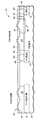
参照によって図面を参照すると、図1は、本発明の好適な実施形態に従ってp型基板に形成された集積回路(IC)2の断面図である。n型基板では、p型埋込み層に代わってn型埋込み層が使用される。図1に示すように、IC2は、ディジタルコンポーネント4、アナログコンポーネント6、受動RFコンポーネント8、および能動RFコンポーネント10を支援する。IC2は、高抵抗基板14を介した上記の種々のコンポーネントの間の電気的相互作用を低減させる隔離構造12を有することによって、ディジタルコンポーネント4、アナログコンポーネント6、受動RFコンポーネント8、および能動RFコンポーネント10を支援することが可能である。基板14は電気的には、基本的にIC2にある全素子を接続している抵抗器である。上記の種々のコンポーネントを隔離および絶縁することにより、ディジタルコンポーネント4、アナログコンポーネント6、受動RFコンポーネント8、および能動RFコンポーネント10を1つのIC2に実装することが可能となる。これらのコンポーネントを低抵抗埋込み層16または高抵抗基板14の内部もしくは上部に戦略的に配置することにより、上記の種々のコンポーネントを1つのIC2に実装する一方でその個々の性能を最大限に高めることができる。低抵抗層16、高抵抗基板14およびウェル構造20を使用することにより、種々のコンポーネントを絶縁および隔離し、これらを1つのIC2に実装することが可能となる。
Referring to the drawings by reference, FIG. 1 is a cross-sectional view of an integrated circuit (IC) 2 formed on a p-type substrate in accordance with a preferred embodiment of the present invention. In the n-type substrate, an n-type buried layer is used instead of the p-type buried layer. As shown in FIG. 1, IC 2 supports digital component 4, analog component 6,
CMOSディジタル回路要素22が低抵抗埋込み層16上に設けられている。受動RF回路要素8、例えばインダクタ24が、高抵抗基板14上に設けられている。NMOS26またはNPN BJT28などのアナログ回路要素6が、高抵抗基板14にある隔離されたウェル30内に設けられている。ヘテロ接合バイポーラトランジスタ(HBT)32などの能動RF要素10が、高抵抗部14内に設けられており、HBT32の性能を最大限に高める。
A CMOS
CMOS22は、PMOS34とNMOS素子36とからなる。各MOS素子22は、ゲート38、ソース40およびドレイン42を有する。低抵抗埋込み層16にCMOSディジタル回路要素22を配置することには利点が幾つかある。第一に、埋込み層16は、CMOS素子22間でのラッチアップの発生を低減させる。ラッチアップとは、CMOS22のNMOS36部分とPMOS34部分との間に基板14を介して大きな電流が流れ、CMOS22の性能を低下させる状態である。ラッチアップによって、CMOS回路22が特定の論理状態に固定されたままとなる。簡単にいえば、ラッチアップは、寄生性のPNPN様の動作に関わる内部フィードバック機構によって生ずる。しかし、埋込み層16は、電流が通ることができる低抵抗の経路をCMOS22の下部に提供することにより、ラッチアップの発生を低減させる。
The
第二に、低抵抗埋込み層16はノイズシンクのように動作する。CMOSディジタル回路22は、素子22のレイル・ツー・レイル電圧振幅が大きいため、非常に高いレベルのノイズを生じさせる。この電気的ノイズは、この素子から低抵抗埋込み層16に向かうようになる。第三に、埋込み層16は、ディジタルCMOSコンポーネント22の直下に配置される。このように、埋込み層16のノイズが、通常はディジタルCMOSコンポーネント22に制限される。
Second, the low-resistance buried
アナログCMOSコンポーネント44が高抵抗基板14上に設けられている。高抵抗基板14は埋込み層16から出るノイズを減衰させ、これにより、ディジタルCMOSコンポーネント22からアナログCMOSコンポーネント44を隔離および絶縁する。これ以外のディジタルCMOSコンポーネント22は埋込み層16からのノイズに晒されるが、ディジタルの特性により、CMOSコンポーネント22はノイズの影響を比較的受けにくい。
An
埋込み層16は、ディジタルCMOS22と結合されて記載されているが、種々のウェル構造を使用して、IC2内の、電気的ノイズを多く発生させる他の素子を隔離してもよい。電気的ノイズを多く発生させる素子の例に、チャージポンプがある。nウェル46の領域とpウェル48の領域とに囲まれた隔離されたウェル20内にチャージポンプを配置することによって、チャージポンプが発生させる電気的ノイズから周囲のコンポーネントを隔離することができる。さらに隔離を強化するために、p+埋込み層16の上部にpウェル48が配置される。pウェル48は低抵抗であるため、IC2内で発生し、pウェル48によって収集された電気的ノイズを、IC2から有効に除去することができる。このように、pウェル48とp+埋込み層16とを組み合わせることによって、ディジタルコンポーネント4、アナログコンポーネント6、受動RFコンポーネント8および能動RFコンポーネント10を1つのIC2に実装したときに、ノイズの伝搬が低減される。
Although the buried
ヘテロ接合バイポーラトランジスタ32などの能動RF要素10が、高抵抗基板14上に設けられている。図1には、p型基板上に設けたNPN HBT素子が記載されている。高抵抗基板14上にHBT32を配置することによって、コレクタウェル60と基板14との間のキャパシタンス(Ccsとして示す)が最少となる。コレクタ60と基板14とのキャパシタンスを最少にすることにより、HBT32の性能が最大限に向上する。さらに、能動RFコンポーネント10は、pウェル48によって囲まれており、このpウェル48は、IC2の他の場所で発生した外部ノイズからHBT32を隔離する作用を果たす。
An
pウェル48によるHBT32の隔離をさらに強化するために、p+埋込み層16の上にpウェル48が設けられている。p+埋込み層16は低抵抗であるため、pウェル48によって収集されたIC2内の電気的ノイズが、ここでIC2から除去される。このように、pウェル48は、IC2の他の場所で発生し、HBT32に到達するノイズの量を低減させる。また、IC2内の電気的ノイズは、低抵抗であるためp+埋込み層16によっても収集され、ここでIC2から除去される。このように、p+埋込み層16はIC2の他の場所で発生し、HBT32に到達するノイズの量を低減させる。
In order to further enhance the isolation of the
受動RF回路要素8、例えばインダクタ70が、高抵抗領域16の内部もしくは上部に設けられている。受動RFコンポーネント8の性能の評価基準となるのが、素子のQである。高周波RF回路においては、Qが低い受動コンポーネント8は望ましくない。Qの低い素子では、通常、信号の損失を補償するために入力ステージ(input stage)の追加が必要となる。このような余分の入力ステージにより、チップスペースと、デバイスのコストとが増大する。インダクタ70のQを低減し、これによりインダクタ70の性能を向上させるには、IC2の他の素子が発生させる電気的ノイズからインダクタ70を隔離することが望ましい。
A passive
インダクタ70は、インダクタ70を形成するコイルを表す一連の波線として示される。高抵抗基板14は、IC2の他の場所で発生したノイズ信号を減衰させて、インダクタ70などの受動RF要素8に到達するのを防止する。このように、基板14は、インダクタ70が受けるノイズを低減させることにより、インダクタ70の性能を向上させQを改善する。Qの改善は、高周波では最も顕著である。図面には記載されていないが、別の受
動RF要素8にコンデンサがあり、上記の原理はコンデンサにも当てはまる。さらに、基板14は、IC2の他の場所で発生したノイズを減衰させることにより、クロストークも低減させる。
Inductor 70 is shown as a series of wavy lines that represent the coils that form inductor 70. The
さらに、インダクタのQは、インダクタを高抵抗基板14の上部に配置することによりさらに改善される。基板14は、高抵抗であるため、インダクタ70の性能を低下させる電気的渦電流の発生を阻止する。
Furthermore, the inductor Q is further improved by placing the inductor on top of the
インダクタ70などの受動RF要素8を隔離するその他の方法として、pウェル隔離構造72とp+埋込み層74とによって高抵抗基板14を囲む方法がある。pウェル72とp+埋込み層74との併用は、インダクタ70がIC2の他の領域から受ける電気的ノイズの量を低減させる。この構造は、低抵抗であるため、これらの信号を集めてIC2から除去することができる。このように、pウェル72とp+埋込み層74との併用は、インダクタ70へ到達するノイズの量を低減させる。
As another method of isolating the
パターニングされた埋込み層16、高抵抗基板14、pウェル46,72およびnウェル48からなる隔離構造12は、アナログコンポーネント6およびRFコンポーネント8,10の動作を阻害するIC2のノイズの問題とクロストークの問題とを軽減する。さらに、隔離構造12は、ディジタルコンポーネント4、アナログコンポーネント6、受動RFコンポーネント8、および能動RFコンポーネント10の全体的な性能を、これらのコンポーネントの種々の寄生性による問題に対処することによって改善させる。
The
図2に示す好適な実施形態においては、1つの埋込み層16が、1つのディジタル回路ブロック76にある全ディジタルCMOSコンポーネント22の下に延在している。1つの埋込み層16が1つのディジタル回路ブロック76全体の下に延在していることにより、これら素子22内でのラッチアップの発生が大幅に低減される。ブロック76で発生する電気的ノイズは全て、埋込み層16を介してブロック76内の他の領域および素子22に伝わる。しかし、ディジタルCMOSコンポーネント22の特性により、この素子22の性能が大きく低下することはない。埋込み層16を1つ備えることで、素子の構成が単純なものとなり、製造プロセスが簡略化されると共に全体的なコストが削減される。ディジタルブロック76には、CMOS22、抵抗器77、および他のディジタルコンポーネント79が存在する。
In the preferred embodiment shown in FIG. 2, one buried
図3に示す別法による実施形態においては、埋込み層16は、一連のブロック78に分割されており、1つのディジタル回路ブロック22にあるディジタルCMOSコンポーネント22の下に延在している。これらのブロック78の間には、高抵抗領域14が存在する。1つのディジタル回路ブロック76内の電気的ノイズの伝搬を制限するために、埋込み層16を一連の小ブロック78に分割することが好ましいことがあり得る。電気的ノイズは埋込み層ブロック78内では比較的容易に伝わるが、埋込み層ブロック78の間に設けられている高抵抗領域14が、埋込み層ブロック78から別の埋込み層ブロック78にノイズが伝わるのを阻止し、ノイズを減衰させる。このため、高抵抗領域14によりブロック間を不連続にすること(delineation)は、1つのディジタルブロック76内でのノイズの伝搬を制限する。
In the alternative embodiment shown in FIG. 3, the buried
図4に、本発明の好適な実施形態における隔離されたアナログ回路要素6の断面を示す。本例ではp型基板を使用している。種々の領域が、ディジタルCMOS22が発生させたノイズからアナログ回路を遮蔽している。第一に、アナログ回路6が高抵抗部14内に設けられている。基板14は高抵抗であるため、他の素子から発生した電気信号を減衰させる。この大きな減衰によって、素子クロストークの発生が低減される。図に示すように、NMOS素子26はゲート80、ソース82およびドレイン84からなる。バルク領域
88と電気的な連通を取るため、バルクコンタクト86が設けられている。NMOS素子26が、隔離されたpウェル90内に設けられている。隔離されたpウェル90の下にはn隔離領域92が存在する。n隔離領域92はnウェルリング98およびnウェル46の少なくとも一方と接続されており、隔離されたpウェル90を本例に示すp型基板14から完全に隔離している。n隔離領域92とnウェル46とは、IC2の他の場所で発生した電気信号を集める。次にこの電気信号は、コンタクト94によりIC2から除去される。このように、IC2の他の場所で発生した電気信号がIC2から除去され、これによってアナログ回路6が遮蔽される。
FIG. 4 shows a cross section of an isolated analog circuit element 6 in a preferred embodiment of the present invention. In this example, a p-type substrate is used. Various areas shield the analog circuitry from the noise generated by the
好適な実施形態においては、nウェル46およびnウェルリング98の全てが同じ電位レベルに維持される。nウェル46とウェルリング98とはn隔離領域92を介して接続されている。コンタクト94は、nウェル46、nウェルリング98、またはn隔離領域92によって集められた全電気信号をIC2から除去する。このように、nウェル46、nウェルリング98、またはn隔離領域92は、ディジタルCMOS22もしくはノイズを多く出す電気的コンポーネント(チャージポンプなど)が発生させる電気的ノイズから、IC2の種々の回路コンポーネントを絶縁および隔離する作用を果たす。
In the preferred embodiment, n-well 46 and n-
図5に、本発明の好適な実施形態に従って作製した隔離されたディジタル回路ブロック76を示す。好適な実施形態においては、ディジタルブロック76は、ディジタルCMOS回路22のほか、抵抗器77、他のディジタル電気コンポーネント79からなる。ディジタルブロック76は1つのp+埋込み層16上に設けられている。1つのディジタル回路ブロック76全体の下に延在する1つのp+埋込み層16を設けることにより、素子22内でラッチアップが発生する可能性が大幅に低減する。ディジタルCMOS22はレイル・ツー・レイルの電圧振幅が大きいため、回路22は電気的ノイズを多く発生させる。ディジタルCMOS22が発生するこの電気的ノイズは、阻止または除去されなければ、基板14を介してIC2のアナログコンポーネント6、RFコンポーネント8,10に伝わる。
FIG. 5 illustrates an isolated
ノイズを多く出すディジタルCMOS回路22を、IC2の他の部分から隔離するために、ディジタルブロック76の周りにnウェルリング98が設けられている。このnウェルリング98は、ディジタルCMOS22が発生させる電気信号を集める。nウェルリング98に接続されたコンタクト94がIC2から電気信号を除去する。nウェルリング98は、隔離pウェルリング100によって囲まれている。隔離pウェルリング100の外側にp+ソースドレインリング102が配置されている。ウェルリング98,100,102は、協調してディジタルCMOS22が発生させる電気信号を収集および除去する。
An n-
図6に、本発明の好適な実施形態に従って作製された集積回路2内に形成されたヘテロ接合バイポーラトランジスタ(HBT)32を示す。HBT32は、エミッタ106、ベース108、およびコレクタ110を有する疑似自己整合型構造104からなる。自己整合型構造104は、構造を簡略化し、トポロジ(topography)を単純化する。HBT32素子は、CMOSコンポーネント22と共に実装可能であるため、能動RFの動作のために使用することが望ましい。
FIG. 6 shows a heterojunction bipolar transistor (HBT) 32 formed in an
エミッタ112、ベース114、およびコレクタのコンタクト領域116が、HBT32の表面の上に設けられている。ビア118が、エミッタ112、ベース114、およびコレクタのコンタクト領域を接続している。これらのビアを絶縁しているのが、誘電電材122である。HBT32の性能低下を招く主因となるのが、コレクタウェル124と基板14との間のキャパシタンスである。HBT32の性能を最大限に高めるためには、コレクタ124と基板14との間のキャパシタンスを最少にする必要がある。高抵抗基板14上にHBT32を直接配置することにより、コレクタ124と基板14との間のこの寄
生性のキャパシタンスが最少となる。
An
次に、pウェル48とp+埋込み層16とを使用することにより、HBT32が、IC2の他の素子が発生させる電気的ノイズから隔離および絶縁されている。Pウェル48およびp+埋込み層16は、IC2の他の場所で発生した電気信号を集めて、これらをシステムから除去し、これによりHBT32を隔離する。このように、電気的ノイズの問題とクロストークの問題とが軽減され、この結果HBT32の性能が向上する。
Next, by using the p-well 48 and the p + buried
図7に、本発明の好適な実施形態に従って作製された集積回路2内に形成されたバラクタ126を示す。「バラクタ」との用語は、バリアブル(可変)リアクトルに由来し、バイアス電圧によりリアクタンスを制御可能に変更できる素子を指す。バラクタ126はパラメトリック増幅、高調波発生(harmonic generation)、ミキシング、検波、および電圧可変チューニング(tunning)のアプリケーションに広く用いられている。図7に示すp型基板にある上部のバラクタ126は、ゲート128と、nウェル132上に設けられたベースコンタクト130とを有する。バラクタ126は、p+埋込み層16の上部に設けられている。バラクタ126は、能動RFコンポーネント10と同様、Qを最大限に高めることが望ましい。nウェル132は低抵抗であり、かつnウェル132により絶縁が提供されるため、バラクタ126をnウェル132内に設けることによって、Qが改善される。
FIG. 7 shows a
当業者は、本明細書に記載の方法および構造の一部または全てによって本発明を実施し得ることを理解するが、本発明を様々な形態で実施可能であり、本発明の趣旨並びに範囲から逸脱することなく、種々の変形、置換、並びに変更を行うことができることが当業者によって理解される。記載した実施形態は、限定的なものではなく例示的なものに過ぎず、このため、本発明の範囲は添付の特許請求の範囲によって示される。 Those skilled in the art will appreciate that the invention can be practiced by some or all of the methods and structures described herein, but that the invention can be practiced in various forms and from the spirit and scope of the invention. It will be appreciated by those skilled in the art that various modifications, substitutions, and changes can be made without departing. The described embodiments are merely exemplary rather than limiting and the scope of the invention is therefore indicated by the appended claims.
Claims (5)
前記高抵抗基板上に形成された、パターニングされた低抵抗埋込み層と、前記パターニングされた低抵抗埋込み層と前記高抵抗基板との電荷種類が等しいことと、
前記パターニングされた低抵抗埋込み層の上部に形成されたディジタル回路と、
前記高抵抗基板上に形成されたアナログ回路と、
前記高抵抗基板上に形成された受動RF素子と、
前記ディジタル回路を囲むウェル領域とを有する集積回路。 A high resistance substrate;
A patterned low-resistance buried layer formed on the high-resistance substrate, and the charge types of the patterned low-resistance buried layer and the high-resistance substrate are equal;
A digital circuit formed on top of the patterned low resistance buried layer;
An analog circuit formed on the high-resistance substrate;
A passive RF element formed on the high-resistance substrate;
An integrated circuit having a well region surrounding the digital circuit.
Applications Claiming Priority (2)
| Application Number | Priority Date | Filing Date | Title |
|---|---|---|---|
| US10/178,672 US20030234438A1 (en) | 2002-06-24 | 2002-06-24 | Integrated circuit structure for mixed-signal RF applications and circuits |
| PCT/US2003/016286 WO2004001850A1 (en) | 2002-06-24 | 2003-05-21 | Integrated circuit structure for mixed-signal rf applications and circuits |
Publications (2)
| Publication Number | Publication Date |
|---|---|
| JP2005531143A true JP2005531143A (en) | 2005-10-13 |
| JP2005531143A5 JP2005531143A5 (en) | 2006-06-29 |
Family
ID=29734747
Family Applications (1)
| Application Number | Title | Priority Date | Filing Date |
|---|---|---|---|
| JP2004515710A Withdrawn JP2005531143A (en) | 2002-06-24 | 2003-05-21 | Integrated circuit structures for mixed signal RF applications and circuits |
Country Status (7)
| Country | Link |
|---|---|
| US (1) | US20030234438A1 (en) |
| EP (1) | EP1518276A1 (en) |
| JP (1) | JP2005531143A (en) |
| KR (1) | KR20050013190A (en) |
| CN (1) | CN1547775A (en) |
| AU (1) | AU2003248560A1 (en) |
| WO (1) | WO2004001850A1 (en) |
Cited By (2)
| Publication number | Priority date | Publication date | Assignee | Title |
|---|---|---|---|---|
| JP2006078264A (en) * | 2004-09-08 | 2006-03-23 | Toppan Printing Co Ltd | Dna chip device |
| JP2014120593A (en) * | 2012-12-17 | 2014-06-30 | Renesas Electronics Corp | Semiconductor integrated circuit |
Families Citing this family (9)
| Publication number | Priority date | Publication date | Assignee | Title |
|---|---|---|---|---|
| US7375000B2 (en) * | 2005-08-22 | 2008-05-20 | International Business Machines Corporation | Discrete on-chip SOI resistors |
| US7884440B2 (en) * | 2006-04-26 | 2011-02-08 | Magnachip Semiconductor, Ltd. | Semiconductor integrated circuit |
| KR100854440B1 (en) * | 2006-04-26 | 2008-08-26 | 매그나칩 반도체 유한회사 | Semiconductor integrated circuit |
| KR100876604B1 (en) | 2007-07-13 | 2008-12-31 | (주)페타리 | Semiconductor device and method of manufacturing the same |
| US8129817B2 (en) * | 2008-12-31 | 2012-03-06 | Taiwan Semiconductor Manufacturing Co., Ltd. | Reducing high-frequency signal loss in substrates |
| CN102055414A (en) * | 2010-04-14 | 2011-05-11 | 锐迪科创微电子(北京)有限公司 | Radio-frequency power amplifier module and mobile communication terminal |
| US8679863B2 (en) | 2012-03-15 | 2014-03-25 | International Business Machines Corporation | Fine tuning highly resistive substrate resistivity and structures thereof |
| KR102070477B1 (en) * | 2012-06-28 | 2020-01-29 | 스카이워크스 솔루션즈, 인코포레이티드 | Bipolar transistor on high-resistivity substrate |
| CN104051529B (en) * | 2013-03-13 | 2017-07-28 | 台湾积体电路制造股份有限公司 | RF switches on high-impedance substrate |
Family Cites Families (19)
| Publication number | Priority date | Publication date | Assignee | Title |
|---|---|---|---|---|
| US5218224A (en) * | 1989-06-14 | 1993-06-08 | Kabushiki Kaisha Toshiba | Semiconductor device including inversion preventing layers having a plurality of impurity concentration peaks in direction of depth |
| JPH03222467A (en) * | 1990-01-29 | 1991-10-01 | Mitsubishi Electric Corp | Semiconductor integrated circuit device |
| US5994755A (en) * | 1991-10-30 | 1999-11-30 | Intersil Corporation | Analog-to-digital converter and method of fabrication |
| JP3217560B2 (en) * | 1993-11-15 | 2001-10-09 | 株式会社東芝 | Semiconductor device |
| US5623159A (en) * | 1994-10-03 | 1997-04-22 | Motorola, Inc. | Integrated circuit isolation structure for suppressing high-frequency cross-talk |
| US5559349A (en) * | 1995-03-07 | 1996-09-24 | Northrop Grumman Corporation | Silicon integrated circuit with passive devices over high resistivity silicon substrate portion, and active devices formed in lower resistivity silicon layer over the substrate |
| US5880515A (en) * | 1996-09-30 | 1999-03-09 | Lsi Logic Corporation | Circuit isolation utilizing MeV implantation |
| JPH10199993A (en) * | 1997-01-07 | 1998-07-31 | Mitsubishi Electric Corp | Semiconductor circuit device, manufacture thereof, and mask device for manufacturing semiconductor circuit device |
| US6407441B1 (en) * | 1997-12-29 | 2002-06-18 | Texas Instruments Incorporated | Integrated circuit and method of using porous silicon to achieve component isolation in radio frequency applications |
| US6388290B1 (en) * | 1998-06-10 | 2002-05-14 | Agere Systems Guardian Corp. | Single crystal silicon on polycrystalline silicon integrated circuits |
| US6166415A (en) * | 1998-11-02 | 2000-12-26 | Mitsubishi Denki Kabushiki Kaisha | Semiconductor device with improved noise resistivity |
| US6424022B1 (en) * | 2000-03-12 | 2002-07-23 | Mobilink Telecom, Inc. | Guard mesh for noise isolation in highly integrated circuits |
| US7575969B2 (en) * | 2000-03-02 | 2009-08-18 | Texas Instruments Incorporated | Buried layer and method |
| US20020125537A1 (en) * | 2000-05-30 | 2002-09-12 | Ting-Wah Wong | Integrated radio frequency circuits |
| US6441442B1 (en) * | 2000-05-30 | 2002-08-27 | Programmable Silicon Solutions | Integrated inductive circuits |
| US6525394B1 (en) * | 2000-08-03 | 2003-02-25 | Ray E. Kuhn | Substrate isolation for analog/digital IC chips |
| JP2002198490A (en) * | 2000-12-26 | 2002-07-12 | Toshiba Corp | Semiconductor device |
| US6909150B2 (en) * | 2001-07-23 | 2005-06-21 | Agere Systems Inc. | Mixed signal integrated circuit with improved isolation |
| US6563181B1 (en) * | 2001-11-02 | 2003-05-13 | Motorola, Inc. | High frequency signal isolation in a semiconductor device |
-
2002
- 2002-06-24 US US10/178,672 patent/US20030234438A1/en not_active Abandoned
-
2003
- 2003-05-21 JP JP2004515710A patent/JP2005531143A/en not_active Withdrawn
- 2003-05-21 WO PCT/US2003/016286 patent/WO2004001850A1/en not_active Application Discontinuation
- 2003-05-21 CN CNA03800917XA patent/CN1547775A/en active Pending
- 2003-05-21 KR KR10-2004-7002733A patent/KR20050013190A/en not_active Application Discontinuation
- 2003-05-21 EP EP03761029A patent/EP1518276A1/en not_active Withdrawn
- 2003-05-21 AU AU2003248560A patent/AU2003248560A1/en not_active Abandoned
Cited By (2)
| Publication number | Priority date | Publication date | Assignee | Title |
|---|---|---|---|---|
| JP2006078264A (en) * | 2004-09-08 | 2006-03-23 | Toppan Printing Co Ltd | Dna chip device |
| JP2014120593A (en) * | 2012-12-17 | 2014-06-30 | Renesas Electronics Corp | Semiconductor integrated circuit |
Also Published As
| Publication number | Publication date |
|---|---|
| KR20050013190A (en) | 2005-02-03 |
| CN1547775A (en) | 2004-11-17 |
| WO2004001850A1 (en) | 2003-12-31 |
| EP1518276A1 (en) | 2005-03-30 |
| US20030234438A1 (en) | 2003-12-25 |
| AU2003248560A1 (en) | 2004-01-06 |
Similar Documents
| Publication | Publication Date | Title |
|---|---|---|
| JP4141881B2 (en) | Integrated circuit | |
| US7265433B2 (en) | On-pad broadband matching network | |
| US7052939B2 (en) | Structure to reduce signal cross-talk through semiconductor substrate for system on chip applications | |
| US6310387B1 (en) | Integrated circuit inductor with high self-resonance frequency | |
| US7022566B2 (en) | Integrated radio frequency circuits | |
| EP2741326B1 (en) | Shielding silicon from external RF interference | |
| US20050221787A1 (en) | Integrated radio frequency circuits | |
| US6903459B2 (en) | High frequency semiconductor device | |
| JP2005531143A (en) | Integrated circuit structures for mixed signal RF applications and circuits | |
| US20210313421A1 (en) | Signal isolation apparatus and signal isolation method | |
| US20080116541A1 (en) | Structure for integrating an rf shield structure in a carrier substrate | |
| Hsu et al. | Psub guard ring design and modeling for the purpose of substrate noise isolation in the SOC era | |
| US6909150B2 (en) | Mixed signal integrated circuit with improved isolation | |
| US6800918B2 (en) | EMI and noise shielding for multi-metal layer high frequency integrated circuit processes | |
| KR20090064990A (en) | Inductor for semiconductor device and method for fabricating the same | |
| US6348718B1 (en) | Integrated CMOS circuit for use at high frequencies | |
| JPH0560685B2 (en) | ||
| US5864168A (en) | Apparatus and method for reduced substrate noise coupling | |
| JP2638544B2 (en) | Semiconductor integrated circuit | |
| JP4357768B2 (en) | Semiconductor integrated circuit | |
| US6285071B1 (en) | Substrate-on-insulator semiconductor device with noise decoupling | |
| KR100707594B1 (en) | Thyristor-type isolation sturcture of semiconductor device | |
| JP2002057218A (en) | Integrated radio frequency circuit | |
| JPH04343274A (en) | Semiconductor device |
Legal Events
| Date | Code | Title | Description |
|---|---|---|---|
| A521 | Written amendment |
Free format text: JAPANESE INTERMEDIATE CODE: A523 Effective date: 20060510 |
|
| A621 | Written request for application examination |
Free format text: JAPANESE INTERMEDIATE CODE: A621 Effective date: 20060510 |
|
| A521 | Written amendment |
Free format text: JAPANESE INTERMEDIATE CODE: A523 Effective date: 20060609 |
|
| A761 | Written withdrawal of application |
Free format text: JAPANESE INTERMEDIATE CODE: A761 Effective date: 20061122 |