JP4357768B2 - Semiconductor integrated circuit - Google Patents
Semiconductor integrated circuit Download PDFInfo
- Publication number
- JP4357768B2 JP4357768B2 JP2001177562A JP2001177562A JP4357768B2 JP 4357768 B2 JP4357768 B2 JP 4357768B2 JP 2001177562 A JP2001177562 A JP 2001177562A JP 2001177562 A JP2001177562 A JP 2001177562A JP 4357768 B2 JP4357768 B2 JP 4357768B2
- Authority
- JP
- Japan
- Prior art keywords
- circuit
- frequency
- semiconductor integrated
- metal shield
- integrated circuit
- Prior art date
- Legal status (The legal status is an assumption and is not a legal conclusion. Google has not performed a legal analysis and makes no representation as to the accuracy of the status listed.)
- Expired - Fee Related
Links
Images


Description
【0001】
【発明の属する技術分野】
この発明は、不要結合を抑圧する半導体集積回路に関するものである。
【0002】
【従来の技術】
図7は例えば1982年 IEEE IEDM pp.58−61に示された従来の半導体集積回路を示す斜視図であり、図において、1a,1bは誘電体層、2a,2bはドープ層、3はサブストレート層、4はトレンチ分離、5は半導体集積回路内の第一の回路、6は半導体集積回路内の第二の回路である。
【0003】
次に動作について説明する。
トレンチ分離4が存在しない場合では、半導体集積回路内の第一の回路5内の電流の一部は、ドープ層2aおよびドープ層2b、あるいはサブストレート層3を経て半導体集積回路内の第二の回路6へ漏洩する。ここで、トレンチ分離4が存在することにより、ドープ層2aからドープ層2bに伝わる電流は遮られ、サブストレート層3を伝わる以外になくなる。しかし、サブストレート層3にはほとんどトレンチ分離4が存在し、さらに、サブストレート層3の抵抗率は高いため、電流は大きく減衰する。このため、トレンチ分離4を設けることによって、第一の回路5および第二の回路6間の電流による不要結合の抑圧が可能となる。
【0004】
【発明が解決しようとする課題】
従来の半導体集積回路は以上のように構成されているので、トレンチ分離4により、半導体集積回路内の電流による不要結合を抑圧することができる。しかしながら、半導体集積回路内の容量性の不要結合は抑圧されず、例えば、第一の回路5の電圧変動が第二の回路6に影響を及ぼしてしまうなどの課題があった。
【0005】
この発明は上記のような課題を解決するためになされたもので、容量性の不要結合を抑圧する半導体集積回路を得ることを目的とする。
【0006】
【課題を解決するための手段】
この発明に係る半導体集積回路は、高周波増幅回路と周波数変換回路との間に配置され、少なくともその高周波増幅回路にバイアスを供給するバイアス回路と、当該半導体集積回路の表面にのみ配置され、かつバイアス回路の上部にのみ配置されたメタルシールドと、メタルシールドを高周波的に接地する高周波接地接続手段とを備えたものである。
【0007】
この発明に係る半導体集積回路は、高周波接地接続手段により、メタルシールドを半導体集積回路の外部で高周波的に接地するようにしたものである。
【0008】
【発明の実施の形態】
以下、この発明の実施の一形態を説明する。
実施の形態1.
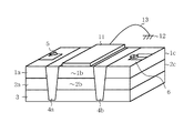
図1はこの発明の実施の形態1による半導体集積回路を示す斜視図であり、図において、1a〜1cは例えば二酸化シリコン等によって形成された誘電体層、2a〜2cは誘電体層1a〜1cの下層に形成されたドープ層、3はドープ層2a〜2cの下層に形成されたサブストレート層、4a,4bは絶縁体で形成され、誘電体層1a〜1cおよびドープ層2a〜2cをそれぞれ分離するトレンチ分離、5は誘電体層1aおよびドープ層2a側に形成された半導体集積回路内の第一の回路、6は誘電体層1cおよびドープ層2c側に形成された半導体集積回路内の第二の回路である。
また、11は誘電体層1b上のトレンチ分離4a,4b近傍、かつトレンチ分離4a,4b間に配置された導電性のメタルシールド、12は半導体集積回路の外部に設けられた高周波接地(高周波接地接続手段)、13はメタルシールド11と高周波接地12とを接続するワイヤー(高周波接地接続手段)である。
【0009】
次に動作について説明する。
図1に示したように、半導体集積回路は多層形成されている。誘電体層1a〜1cは、抵抗率が高いが薄膜によって形成され、ドープ層2a〜2cは、抵抗率がやや低く、サブストレート層3は、抵抗率が高い。
図1に示した半導体集積回路において、トレンチ分離4a,4bが存在しない場合では、半導体集積回路内の第一の回路5内の電流の一部は、ドープ層2aからドープ層2b,2c、あるいはサブストレート層3を経て半導体集積回路内の第二の回路6へ漏洩する。ここで、トレンチ分離4a,4bが存在することにより、ドープ層2aからドープ層2b、およびドープ層2bからドープ層2cに伝わる電流は遮られ、サブストレート層3を伝わる以外になくなる。しかし、サブストレート層3にはほとんどトレンチ分離4a,4bが存在し、さらに、サブストレート層3の抵抗率は高いため、電流は大きく減衰する。このため、トレンチ分離4a,4bを設けることによって、第一の回路5および第二の回路6間の電流による不要結合の抑圧が可能となる。
【0010】
また、第一の回路5および第二の回路6間の容量性の不要結合は、メタルシールド11を介したものとなる。ここで、メタルシールド11は、半導体集積回路の外部に設けられた高周波接地12にワイヤー13によって接続されているため高周波接地されており、第一の回路5および第二の回路6のうちの一方の回路の電圧変動が他方の回路に影響を及ぼすことなく、第一の回路5および第二の回路6間の容量を小さくし、第一の回路5および第二の回路6間の容量性の不要結合を抑圧することができる。
以上により、高周波接地されたメタルシールド11を設けることにより、トレンチ分離4a,4bでは抑圧することのできない第一の回路5および第二の回路6間の容量性の不要結合を抑圧することができる。また、メタルシールド11をトレンチ分離4a,4bの近傍に配置したことによって、メタルシールド11の配置に必要な面積を小さくすることができる。さらに、メタルシールド11を半導体集積回路の外部で高周波的に接地することにより、より効果的にメタルシールドを接地することができ、容量性の不要結合をより効果的に抑圧することができる。また、メタルシールドをトレンチ分離の間に配置したことによって、配置面積を小さくすることができる。
【0011】
なお、図1では、半導体集積回路を、誘電体層1a〜1c、ドープ層2a〜2c、およびサブストレート層3からなるもので説明したが、多層形成される各層の種類および層数は、その他の任意のものであっても、この発明を適用することができる。
また、図1では、トレンチ分離4a,4bを2つ設けたが、どちらか一方でも良く、また、3つ以上設けても良く、トレンチ分離の数が多ければ多いほど電流による不要結合の抑圧度を大きくすることができる。
さらに、図1では、高周波接地12およびワイヤー13により、メタルシールド11を高周波接地したが、定電圧源およびワイヤー13により、メタルシールド11を定電圧にしても良く、この場合でも、第一の回路5および第二の回路6間の容量性の不要結合を抑圧することができる。
【0012】
実施の形態2.
図2はこの発明の実施の形態2による半導体集積回路を示す斜視図であり、図において、14はメタル等の導電性の材料で形成され、誘電体層1bおよびドープ層2bを貫通し、メタルシールド11とサブストレート層3とを接続するサブストレートコンタクト(高周波接地接続手段)である。
その他の構成については、高周波接地12およびワイヤー13を削除した以外、図1と同一である。
【0013】
次に動作について説明する。
メタルシールド11は、半導体集積回路の内部のサブストレート層3にサブストレートコンタクト14によって接続されている。サブストレートコンタクト14は、導電性の材料で形成されており、また、サブストレート層3の下層はグランド(接地)なので(図示せず)、メタルシールド11は、ほぼ高周波接地されていることになる。したがって、第一の回路5および第二の回路6のうちの一方の回路の電圧変動が他方の回路に影響を及ぼすことなく、第一の回路5および第二の回路6間の容量を小さくし、第一の回路5および第二の回路6間の容量性の不要結合を抑圧することができる。
また、半導体集積回路の外部で高周波的に接地する必要がなくなり、半導体集積回路の内部だけで高周波的に接地することができる。また、メタルシールドをトレンチ分離の間に配置したことによって、配置面積を小さくすることができる。
【0014】
実施の形態3.
図3はこの発明の実施の形態3による半導体集積回路を示す斜視図である。
この実施の形態3は、上記実施の形態1に示したように高周波接地12およびワイヤー13により、メタルシールド11を半導体集積回路の外部で高周波接地すると共に、上記実施の形態2に示したようにサブストレートコンタクト14により、メタルシールド11をサブストレート層3に接続し、高周波接地したものである。
このように構成することによって、より効果的にメタルシールド11を接地することができるので、容量性の不要結合をより効果的に抑圧することができる。また、メタルシールドをトレンチ分離の間に配置したことによって、配置面積を小さくすることができる。
【0015】
実施の形態4.
図4はこの発明の実施の形態4による半導体集積回路を示す斜視図であり、図において、1は誘電体層、2はドープ層、3はサブストレート層である。上記誘電体層1およびドープ層2は、トレンチ分離4により分離されていない。
また、メタルシールド11は、高周波接地12およびワイヤー13により、半導体集積回路の外部で高周波接地されると共に、サブストレートコンタクト14により、サブストレート層3に接続され、高周波接地されている。
さらに、15は高アイソレーションが要求される半導体集積回路内の高周波増幅回路、16は高アイソレーションが要求される半導体集積回路内の周波数変換回路である。
【0016】
次に動作について説明する。
例えば、高周波増幅回路15および周波数変換回路16間の容量性の結合により、高周波信号が漏洩する場合を考える。高周波増幅回路15および周波数変換回路16間の容量性の結合は、メタルシールド11を介したものであり、さらに、メタルシールド11が、高周波接地12およびワイヤー13により、半導体集積回路の外部で高周波接地されると共に、サブストレートコンタクト14により、サブストレート層3に接続され、高周波接地されることにより、高周波増幅回路15の電圧変動が周波数変換回路16に影響を及ぼすことがない。また、周波数変換回路16から高周波増幅回路15に対して高周波信号が漏洩する場合も上記と同様である。
このように構成することによって、高周波増幅回路15および周波数変換回路16間相互の容量性の不要結合を抑圧することができる。
なお、高周波接地12は接地とは限らず、定電圧源であっても良い。
また、図4では、高周波増幅回路15および周波数変換回路16間にトレンチ分離4を設けなかったが、1つまたは複数のトレンチ分離4を設けても良く、トレンチ分離の数が多ければ多いほど電流による不要結合の抑圧度を大きくすることができる。
【0017】
実施の形態5.
図5はこの発明の実施の形態5による半導体集積回路を示す平面図であり、図において、21は半導体集積回路、22は高周波増幅回路、23は周波数変換回路、24は高周波増幅回路22および周波数変換回路23間に配置され、高周波増幅回路22にバイアスを供給すると共に、設計に応じて周波数変換回路23にもバイアスを供給するバイアス回路である。また、31はバイアス回路24の上部に配置されたメタルシールドである。なお、メタルシールド31は、高周波接地12およびワイヤー13により、半導体集積回路の外部で高周波接地されている。
【0018】
次に動作について説明する。
この実施の形態5では、メタルシールド31をバイアス回路24の上部に配置することにより、メタルシールド31用の平面方向の配置領域を特別に確保する必要がなく、半導体集積回路の平面方向の小形化が可能である。また、バイアス回路24を流れる信号は主に直流成分であるため、メタルシールド31の配置によってバイアス回路24とメタルシールド31との間に生成される寄生容量の影響を高周波増幅回路22および周波数変換回路23が受けることがない。
また、メタルシールド31は、高周波接地12およびワイヤー13により、半導体集積回路の外部で高周波接地されており、高周波増幅回路22および周波数変換回路23間相互の容量性の不要結合を抑圧することができる。
なお、図5では示していないが、メタルシールド31を、サブストレートコンタクト14により、サブストレート層3に接続し、高周波接地する場合には、バイアス回路24の配置されていない個所でサブストレートコンタクト14を貫通させるようにすれば良い。
【0019】
実施の形態6.
図6はこの発明の実施の形態6による半導体集積回路を示す平面図であり、図において、41はバイアス回路24および高周波増幅回路22の上部に配置されたメタルシールド、42はメタルシールド41と高周波増幅回路22との間に生じる寄生容量がその高周波増幅回路22に影響を及ぼしてしまう部位に設けられたメタルシールドの穴である。なお、メタルシールド41は、高周波接地12およびワイヤー13により、半導体集積回路の外部で高周波接地されている。
【0020】
次に動作について説明する。
この実施の形態6では、メタルシールド41をバイアス回路24および高周波増幅回路22上部に配置し、その高周波増幅回路22上部のうちで、メタルシールド41の配置によってメタルシールド41と高周波増幅回路22との間に生成される寄生容量の影響により高周波増幅回路22の高周波特性の劣化を生じさせる部位に、メタルシールドの穴42を設けたものである。バイアス回路24を流れる信号は主に直流成分であるためメタルシールド41の配置によって生成される寄生容量の影響を受けることがなく、また、高周波増幅回路22に寄生容量の影響のないようにメタルシールドの穴42を配置したメタルシールド41を用いているため、メタルシールド41の配置によって高周波増幅回路22の高周波特性に劣化は生じない。
この実施の形態6では、高周波増幅回路22上部にもメタルシールド41を配置することにより、メタルシールドの大面積化が可能であり、バイアス回路24のみに配置する場合に比べて、容量性の不要結合をより効果的に抑圧することができる。
なお、図6では、バイアス回路24および高周波増幅回路22の上部にメタルシールドの穴42を有するメタルシールド41の配置を行ったが、バイアス回路24および周波数変換回路23の上部にメタルシールドの穴42を有するメタルシールド41を配置しても同様な効果が得られる。
【0021】
【発明の効果】
以上のように、この発明によれば、高周波増幅回路と周波数変換回路との間に配置され、少なくともその高周波増幅回路にバイアスを供給するバイアス回路と、当該半導体集積回路の表面にのみ配置され、かつバイアス回路の上部にのみ配置されたメタルシールドと、メタルシールドを高周波的に接地する高周波接地接続手段とを備えるように構成したので、メタルシールドと高周波接地接続手段とによって、高周波増幅回路および周波数変換回路のうちの一方の回路の電圧変動が他方の回路に影響を及ぼすことなく、高周波増幅回路および周波数変換回路間の容量性の不要結合を抑圧することができる。また、メタルシールドをバイアス回路の上部に配置したことによって、メタルシールドの配置領域を特別に確保する必要が無くなり、半導体集積回路を小型化にすることができる。さらに、バイアス回路を流れる信号は主に直流成分であるため、メタルシールドの配置によってバイアス回路とメタルシールドとの間に生成される寄生容量の影響を高周波増幅回路および周波数変換回路が受けることがない効果がある。
【0022】
この発明によれば、高周波接地接続手段は、メタルシールドを当該半導体集積回路の外部で高周波的に接地するように構成したので、より効果的にメタルシールドを接地することができるので、容量性の不要結合をより効果的に抑圧することができる効果がある。
【図面の簡単な説明】
【図1】 この発明の実施の形態1による半導体集積回路を示す斜視図である。
【図2】 この発明の実施の形態2による半導体集積回路を示す斜視図である。
【図3】 この発明の実施の形態3による半導体集積回路を示す斜視図である。
【図4】 この発明の実施の形態4による半導体集積回路を示す斜視図である。
【図5】 この発明の実施の形態5による半導体集積回路を示す平面図である。
【図6】 この発明の実施の形態6による半導体集積回路を示す平面図である。
【図7】 従来の半導体集積回路を示す斜視図である。
【符号の説明】
1,1a〜1c 誘電体層、2,2a〜2c ドープ層、3 サブストレート層、4a,4b トレンチ分離、5 第一の回路、6 第二の回路、11,31,41 メタルシールド、12 高周波接地(高周波接地接続手段)、13 ワイヤー(高周波接地接続手段)、14 サブストレートコンタクト(高周波接地接続手段)、15,22 高周波増幅回路、16,23 周波数変換回路、21 半導体集積回路、24 バイアス回路、42 穴。[0001]
BACKGROUND OF THE INVENTION
The present invention relates to a semiconductor integrated circuit that suppresses unnecessary coupling.
[0002]
[Prior art]
FIG. 7 shows, for example, 1982 IEEE IEDM pp. 58 is a perspective view showing a conventional semiconductor integrated circuit shown in 58-61, in which 1a and 1b are dielectric layers, 2a and 2b are doped layers, 3 is a substrate layer, 4 is trench isolation, and 5 is A
[0003]
Next, the operation will be described.
In the case where the trench isolation 4 does not exist, a part of the current in the
[0004]
[Problems to be solved by the invention]
Since the conventional semiconductor integrated circuit is configured as described above, unnecessary coupling due to current in the semiconductor integrated circuit can be suppressed by the trench isolation 4. However, capacitive unnecessary coupling in the semiconductor integrated circuit is not suppressed, and there is a problem that, for example, voltage fluctuation of the
[0005]
The present invention has been made to solve the above-described problems, and an object of the present invention is to obtain a semiconductor integrated circuit that suppresses unnecessary capacitive coupling.
[0006]
[Means for Solving the Problems]
A semiconductor integrated circuit according to the present invention is disposed between a high-frequency amplifier circuit and a frequency conversion circuit, is provided with at least a bias circuit for supplying a bias to the high-frequency amplifier circuit, and is disposed only on the surface of the semiconductor integrated circuit. A metal shield disposed only in the upper part of the circuit and high-frequency ground connection means for grounding the metal shield in high frequency are provided.
[ 0007 ]
In the semiconductor integrated circuit according to the present invention, the metal shield is grounded at a high frequency outside the semiconductor integrated circuit by the high frequency ground connection means.
[ 0008 ]
DETAILED DESCRIPTION OF THE INVENTION
An embodiment of the present invention will be described below.
1 is a perspective view showing a semiconductor integrated circuit according to a first embodiment of the present invention. In the figure, reference numerals 1a to 1c denote dielectric layers formed of, for example, silicon dioxide, and 2a to 2c denote dielectric layers 1a to 1c. 3 is a substrate layer formed below the doped
Further, 11 is a conductive metal shield disposed near and between the
[ 0009 ]
Next, the operation will be described.
As shown in FIG. 1, the semiconductor integrated circuit is formed in multiple layers. The dielectric layers 1a to 1c have a high resistivity but are formed of a thin film, the doped
In the semiconductor integrated circuit shown in FIG. 1, when the
[ 0010 ]
Further, the capacitive unnecessary coupling between the
As described above, by providing the
[ 0011 ]
In FIG. 1, the semiconductor integrated circuit has been described as including the dielectric layers 1 a to 1 c, the doped
In FIG. 1, two
Further, in FIG. 1, the
[ 0012 ]
2 is a perspective view showing a semiconductor integrated circuit according to a second embodiment of the present invention. In the figure,
Other configurations are the same as those in FIG. 1 except that the high-
[ 0013 ]
Next, the operation will be described.
The
Further, it is not necessary to ground at high frequency outside the semiconductor integrated circuit, and it is possible to ground at high frequency only inside the semiconductor integrated circuit. Moreover, the arrangement area can be reduced by arranging the metal shield during the trench isolation.
[ 0014 ]
3 is a perspective view showing a semiconductor integrated circuit according to
In the third embodiment, the
By configuring in this way, the
[ 0015 ]
Embodiment 4 FIG.
4 is a perspective view showing a semiconductor integrated circuit according to Embodiment 4 of the present invention. In the figure, 1 is a dielectric layer, 2 is a doped layer, and 3 is a substrate layer. The
The
Further, 15 is a high-frequency amplifier circuit in a semiconductor integrated circuit that requires high isolation, and 16 is a frequency conversion circuit in the semiconductor integrated circuit that requires high isolation.
[ 0016 ]
Next, the operation will be described.
For example, consider a case where a high-frequency signal leaks due to capacitive coupling between the high-
With this configuration, it is possible to suppress unnecessary capacitive coupling between the high-
The high-
In FIG. 4, the trench isolation 4 is not provided between the high-
[ 0017 ]
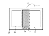
5 is a plan view showing a semiconductor integrated circuit according to
[ 0018 ]
Next, the operation will be described.
In the fifth embodiment, by arranging the
The
Although not shown in FIG. 5, when the
[ 0019 ]
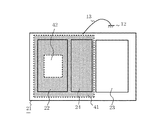
FIG. 6 is a plan view showing a semiconductor integrated circuit according to
[ 0020 ]
Next, the operation will be described.
In the sixth embodiment, the
In the sixth embodiment, it is possible to increase the area of the metal shield by disposing the
In FIG. 6, the
[ 0021 ]
【The invention's effect】
As described above, according to the present invention, it is disposed between the high-frequency amplifier circuit and the frequency conversion circuit, and is disposed only at least on the surface of the semiconductor integrated circuit, the bias circuit for supplying a bias to the high-frequency amplifier circuit, In addition, since the metal shield disposed only on the upper side of the bias circuit and the high-frequency ground connection means for grounding the metal shield at high frequency are provided, the high-frequency amplifier circuit and the frequency are provided by the metal shield and the high-frequency ground connection means. Capacitive unnecessary coupling between the high-frequency amplifier circuit and the frequency conversion circuit can be suppressed without the voltage fluctuation of one of the conversion circuits affecting the other circuit. Further, since the metal shield is arranged on the upper part of the bias circuit, it is not necessary to specially secure the metal shield arrangement region, and the semiconductor integrated circuit can be miniaturized. Furthermore, since the signal flowing through the bias circuit is mainly a direct current component, the high frequency amplifier circuit and the frequency conversion circuit are not affected by the parasitic capacitance generated between the bias circuit and the metal shield due to the arrangement of the metal shield. effective.
[ 0022 ]
According to the present invention, since the high frequency ground connection means is configured to ground the metal shield at a high frequency outside the semiconductor integrated circuit, the metal shield can be grounded more effectively. There is an effect that unnecessary coupling can be suppressed more effectively.
[Brief description of the drawings]
FIG. 1 is a perspective view showing a semiconductor integrated circuit according to a first embodiment of the present invention.
FIG. 2 is a perspective view showing a semiconductor integrated circuit according to a second embodiment of the present invention.
FIG. 3 is a perspective view showing a semiconductor integrated circuit according to a third embodiment of the present invention.
FIG. 4 is a perspective view showing a semiconductor integrated circuit according to a fourth embodiment of the present invention.
FIG. 5 is a plan view showing a semiconductor integrated circuit according to a fifth embodiment of the present invention.
FIG. 6 is a plan view showing a semiconductor integrated circuit according to a sixth embodiment of the present invention.
FIG. 7 is a perspective view showing a conventional semiconductor integrated circuit.
[Explanation of symbols]
1, 1a-1c Dielectric layer, 2, 2a-2c Doped layer, 3 Substrate layer, 4a, 4b Trench isolation, 5 First circuit, 6 Second circuit, 11, 31, 41 Metal shield, 12 High frequency Ground (high-frequency ground connection means), 13 wires (high-frequency ground connection means), 14 substrate contact (high-frequency ground connection means), 15, 22 high-frequency amplifier circuit, 16, 23 frequency conversion circuit, 21 semiconductor integrated circuit, 24
Claims (2)
Priority Applications (1)
| Application Number | Priority Date | Filing Date | Title |
|---|---|---|---|
| JP2001177562A JP4357768B2 (en) | 2001-06-12 | 2001-06-12 | Semiconductor integrated circuit |
Applications Claiming Priority (1)
| Application Number | Priority Date | Filing Date | Title |
|---|---|---|---|
| JP2001177562A JP4357768B2 (en) | 2001-06-12 | 2001-06-12 | Semiconductor integrated circuit |
Publications (2)
| Publication Number | Publication Date |
|---|---|
| JP2002368115A JP2002368115A (en) | 2002-12-20 |
| JP4357768B2 true JP4357768B2 (en) | 2009-11-04 |
Family
ID=19018388
Family Applications (1)
| Application Number | Title | Priority Date | Filing Date |
|---|---|---|---|
| JP2001177562A Expired - Fee Related JP4357768B2 (en) | 2001-06-12 | 2001-06-12 | Semiconductor integrated circuit |
Country Status (1)
| Country | Link |
|---|---|
| JP (1) | JP4357768B2 (en) |
Families Citing this family (1)
| Publication number | Priority date | Publication date | Assignee | Title |
|---|---|---|---|---|
| KR100734507B1 (en) | 2005-05-12 | 2007-07-03 | 하이맥스 테크놀로지스, 인코포레이션 | A structure for current leakage prevention of a high voltage device |
-
2001
- 2001-06-12 JP JP2001177562A patent/JP4357768B2/en not_active Expired - Fee Related
Also Published As
| Publication number | Publication date |
|---|---|
| JP2002368115A (en) | 2002-12-20 |
Similar Documents
| Publication | Publication Date | Title |
|---|---|---|
| JP5209301B2 (en) | Technology and RF circuit design to reduce substrate crosstalk for mixed signals | |
| US6967392B2 (en) | Seal ring structure for radio frequency integrated circuits | |
| JP4215495B2 (en) | WIRING STRUCTURE, ITS MANUFACTURING METHOD, AND SEMICONDUCTOR DEVICE AND WIRING BOARD HAVING WIRING STRUCTURE | |
| US20080012097A1 (en) | Semiconductor device and wireless device using the semiconductor device | |
| TWI694587B (en) | Semiconductor device | |
| US20080116541A1 (en) | Structure for integrating an rf shield structure in a carrier substrate | |
| KR20020079381A (en) | Inductance element and semiconductor device | |
| JP4357768B2 (en) | Semiconductor integrated circuit | |
| JP5194009B2 (en) | Semiconductor device having electrode pad, and wireless circuit device including the semiconductor device | |
| JP4381592B2 (en) | Semiconductor device | |
| US8188565B2 (en) | Semiconductor chip and shielding structure thereof | |
| KR100632464B1 (en) | Integrated circuit including passive device shield structure and method of manufacturing the same | |
| JP2004303744A (en) | Monolithic microwave integrated circuit and its fabrication method | |
| JP2638544B2 (en) | Semiconductor integrated circuit | |
| JP3211756B2 (en) | Semiconductor integrated circuit device | |
| US20070132069A1 (en) | Semiconductor chip and shielding structure thereof | |
| JP4464104B2 (en) | Microwave integrated circuit | |
| US6906610B1 (en) | Inductor element | |
| JP4722522B2 (en) | High frequency semiconductor integrated circuit | |
| JP2005033081A (en) | Semiconductor device | |
| JP6057779B2 (en) | Semiconductor device | |
| JPH03502396A (en) | electronic equipment | |
| CN110660794A (en) | Semiconductor device with a plurality of semiconductor chips | |
| JP2006203082A (en) | Integrated element | |
| JPH08255873A (en) | Semiconductor integrated circuit device |
Legal Events
| Date | Code | Title | Description |
|---|---|---|---|
| A621 | Written request for application examination |
Free format text: JAPANESE INTERMEDIATE CODE: A621 Effective date: 20040708 |
|
| A977 | Report on retrieval |
Free format text: JAPANESE INTERMEDIATE CODE: A971007 Effective date: 20061115 |
|
| A131 | Notification of reasons for refusal |
Free format text: JAPANESE INTERMEDIATE CODE: A131 Effective date: 20061121 |
|
| A521 | Written amendment |
Free format text: JAPANESE INTERMEDIATE CODE: A523 Effective date: 20070122 |
|
| A131 | Notification of reasons for refusal |
Free format text: JAPANESE INTERMEDIATE CODE: A131 Effective date: 20070731 |
|
| A521 | Written amendment |
Free format text: JAPANESE INTERMEDIATE CODE: A523 Effective date: 20070928 |
|
| A521 | Written amendment |
Free format text: JAPANESE INTERMEDIATE CODE: A821 Effective date: 20071003 |
|
| RD02 | Notification of acceptance of power of attorney |
Free format text: JAPANESE INTERMEDIATE CODE: A7422 Effective date: 20071003 |
|
| RD04 | Notification of resignation of power of attorney |
Free format text: JAPANESE INTERMEDIATE CODE: A7424 Effective date: 20071003 |
|
| RD04 | Notification of resignation of power of attorney |
Free format text: JAPANESE INTERMEDIATE CODE: A7424 Effective date: 20080806 |
|
| A131 | Notification of reasons for refusal |
Free format text: JAPANESE INTERMEDIATE CODE: A131 Effective date: 20090512 |
|
| A521 | Written amendment |
Free format text: JAPANESE INTERMEDIATE CODE: A523 Effective date: 20090629 |
|
| TRDD | Decision of grant or rejection written | ||
| A01 | Written decision to grant a patent or to grant a registration (utility model) |
Free format text: JAPANESE INTERMEDIATE CODE: A01 Effective date: 20090728 |
|
| A01 | Written decision to grant a patent or to grant a registration (utility model) |
Free format text: JAPANESE INTERMEDIATE CODE: A01 |
|
| A61 | First payment of annual fees (during grant procedure) |
Free format text: JAPANESE INTERMEDIATE CODE: A61 Effective date: 20090805 |
|
| FPAY | Renewal fee payment (event date is renewal date of database) |
Free format text: PAYMENT UNTIL: 20120814 Year of fee payment: 3 |
|
| R150 | Certificate of patent or registration of utility model |
Ref document number: 4357768 Country of ref document: JP Free format text: JAPANESE INTERMEDIATE CODE: R150 Free format text: JAPANESE INTERMEDIATE CODE: R150 |
|
| FPAY | Renewal fee payment (event date is renewal date of database) |
Free format text: PAYMENT UNTIL: 20120814 Year of fee payment: 3 |
|
| FPAY | Renewal fee payment (event date is renewal date of database) |
Free format text: PAYMENT UNTIL: 20130814 Year of fee payment: 4 |
|
| R250 | Receipt of annual fees |
Free format text: JAPANESE INTERMEDIATE CODE: R250 |
|
| R250 | Receipt of annual fees |
Free format text: JAPANESE INTERMEDIATE CODE: R250 |
|
| R250 | Receipt of annual fees |
Free format text: JAPANESE INTERMEDIATE CODE: R250 |
|
| R250 | Receipt of annual fees |
Free format text: JAPANESE INTERMEDIATE CODE: R250 |
|
| R250 | Receipt of annual fees |
Free format text: JAPANESE INTERMEDIATE CODE: R250 |
|
| LAPS | Cancellation because of no payment of annual fees |